Submitted:
16 October 2025
Posted:
17 October 2025
You are already at the latest version
Abstract
Development of microwave metamaterials is at an exciting moment, where the use and design of metamaterials is spreading from the antennas and electromagnetics communities and increasingly being used by communications, control and systems engineers. This is driven by exciting applications such as Reconfigurable Intelligent Surfaces (RIS) and steerable satellite antennas, but presents challenges in terms of knowledge exchange, technology translation and production scale-up. This roadmap brings together contributions from academia, government and industry across the UK to map the state-of-the-art, draw key challenges still to be solved, and set out recommendations for the next steps in fundamental and applied research. This is part of a joint benture by the UK Metamaterials Network and the Institute of Physics to map the whole breadth of research covered by the umbrella term “metamaterials”.
Keywords:
metamaterials
; metasurfaces
; microwave
; wireless
; terahertz
1. Introduction
Stephen D Henthorn1, Qammer H Abbasi2 and Akram Alomainy3
1School of Electrical and Electronic Engineering, University of Sheffield (s.henthorn@sheffield.ac.uk)
2James Watt School of Engineering, University of Glasgow (Qammer.Abbasi@glasgow.ac.uk)
3School of Electronic Engineering and Computer Science, Queen Mary University of London (a.alomainy@qmul.ac.uk)
Commonly, the electromagnetic properties of a microwave metamaterial are defined by its structure rather than by its chemical composition. Due to the nature of microwaves – electromagnetic radiation at frequencies between 300 MHz and 300 GHz – metamaterials are usually composed of a combination of conductive and dielectric materials, with subwavelength patterns defining how a wave interacts with it. A metamaterial which is very thin with respect to the operating wavelength is usually referred to as a metasurface. This roadmap focusses on microwave metasurfaces due to wavelengths being in the order of cm, most emerging applications utilise electrically thin structures rather than thicker, 3 dimensional materials.
While the term “metamaterial” was first coined around the turn of the last millennium [1] (with “metasurface” following soon after), antennas engineers have been designing engineered structures which would now be called metasurfaces since at least the work of Ben Munk in the 1970s [2], and with the broadest definitions since artificial dielectric lenses were developed by Winston E. Kock at Bell Telephone Laboratories in the 1940s [3]. This historic link to telecommunications means similar techniques are used at lower frequencies, so this roadmap also includes metasurfaces for other wireless applications.
It is currently a very exciting time for microwave and wireless metasurfaces. While engineered structures such as frequency selective surfaces and high impedance surfaces have long been used for specialist applications such as radomes and low-profile antennas, particularly in the defence sector, we are now starting to see metasurface products more widely available. This is largely driven by telecommunications, particularly steerable antennas for satellite communications. Meanwhile, since 2019 there has been an explosion of interest in metasurfaces from the wireless communications theory community due to the concept of Reconfigurable Intelligent Surfaces (RIS, also formerly called Large Intelligent Surfaces or Intelligent Reflecting Surfaces) – metasurfaces which can vary the reflected phase from many independently controlled elements, enabling some control of the wireless propagation channel. This transition from people working with metasurfaces being electromagnetics scientists or engineers, to communications and systems engineers, presents new challenges in terms of knowledge exchange, technology translation and production scale-up.
As such, it is timely to bring together a roadmap giving an overview of microwave and wireless metasurface research in the UK. This is part of a joint venture by the UK Metamaterials Network and the Institute of Physics to map the whole breadth of research covered by the umbrella term “metamaterials”. We seek to provide both a snapshot of current research, and begin to chart a way forward for researchers and policy makers to overcome the barriers to fully exploiting the opportunities of microwave metasurfaces.
In this roadmap, we combine eight contributions from a mixture of universities, government agencies and industrial researchers across the UK. They broadly fit into three cross-cutting themes: i) Applications, discussing the sectors where we anticipate microwave metasurfaces will have the most impact, in particular telecommunications, healthcare and defence; ii) Fundamental science, to capture emerging research which may have impact across many sectors; and iii) Practical concerns, which covers the issues faced as metasurfaces move into mass production, including manufacturing, measurement and system-level integration.
By doing this we can begin to draw key themes about the current state of metasurface research and the key challenges still to be solved. There are scientific challenges remaining, such as the fundamental bandwidth limitations of most metasurfaces due to their resonant behaviour, though some non-resonant structures are now emerging. Similarly, metasurface behaviour is still often heavily contingent on the incident angle of the electromagnetic wave to the material, limiting their usefulness in many applications. Reconfigurability is also often desirable, partly to overcome bandwidth limitations, but combining fast tuning with low losses is still an open challenge, particularly at higher frequencies. There are also practical challenges, such as the need for metasurfaces to maintain performance across a product lifetime. This is particularly important in challenging environments such as healthcare, where biocompatibility is important, and defence. Similarly, sustainability and disposal should be considered at the end of the material’s life cycle. Metasurface properties are also particularly sensitive to variations due to manufacturing tolerances, making reliable mass production difficult. The greatest challenges, though, are in integrating metasurfaces into products and systems – both integration into processes for manufacture, assembly, maintenance and disposal of products; and, for reconfigurable metasurfaces such as RIS, integration into control algorithms, security protocols, site licensing legalities and more. It is particularly important to remember that the control complexity of reconfigurable metasurfaces scales with the number of independently controlled elements, and compute is often a limited resource.
In response to current challenges and research gaps, researchers are identifying possible future solutions extending beyond current state-of-the-art and pushing boundaries. Machine Learning and Artificial Intelligence are common themes across the contributions, potentially simplifying design procedures, proposing new structures to research, assessing robustness to manufacturing tolerances and providing real-time adaptability. Additive manufacturing is also frequently mentioned as a method for producing metasurface structures, though care should be taken to understand the limits to scaling up such approaches. Integration of metasurface fabrication into existing mass production methods, such as roll-to-roll processing, may be a more scalable approach. New kinds of constituent materials, such as flexible, transparent and biocompatible dielectrics and conductors, also offer opportunities for medical and conformal metasurfaces. Finally, new metasurface types and control mechanisms, such as nonlinear surfaces and mechanical reconfiguration, offer new solutions to underlying physical problems.
The following contributions explore these ideas in depth and provide a snapshot of a diverse and excellent research activities in microwave and wireless metasurfaces for both specialists and people newly interested in the area within the UK and globally. We aim for this roadmap to act as a useful primer on the potential of metasurface technology, and give direction to attempts at solving the remaining challenges.
- [1]
- Walser RM, “Electromagnetic metamaterials” Lakhtakia A, Weiglhofer WS, Hodgkinson IJ, editors. Complex Mediums II: Beyond Linear Isotropic Dielectrics. July 2001
- [2]
- Munk BA, Burrell GA, Kornbau TW, ”A general theory of periodic surfaces in stratified media,” Tech. Rept. 784346-1, Ohio State Univ. ElectroScience Lab., Dept of Electrical Eng., prepared under contract AFAL-TR-77-219, Nov. 1977
- [3]
- W. E. Kock, "Metal-Lens Antennas," in Proceedings of the IRE, vol. 34, no. 11, pp. 828-836, Nov. 1946
2. Metasurfaces for 5G+ Wireless Communications
Fraser Burton, Aaron Walker and Yangyishi Zhang
Applied Research, British Telecom (fraser.burton@bt.com)
- Status
Wireless connectivity is fundamental to modern society. For example, over 92% of internet access occurs via mobile devices[1]. Mobile data traffic grows exponentially requiring wireless technologies to be smarter, more reliable and more intelligently engineered.
As the demand for better connectivity grows, fundamental limitations appear due to the inherent nature of wireless communication. Wireless environments are generally treated as an uncontrollable medium that can only be described statistically. Sophisticated processing methods are used to compensate for the uncertain variation in a signal during its transit between transmitter and receiver. This processing requires complex hardware, adding cost and latency and consuming power. Higher frequency transmission supports higher data rates but leads to greater attenuation and shadowing. This reduces the coverage area of a transmitter and increases the energy demand of network infrastructure.
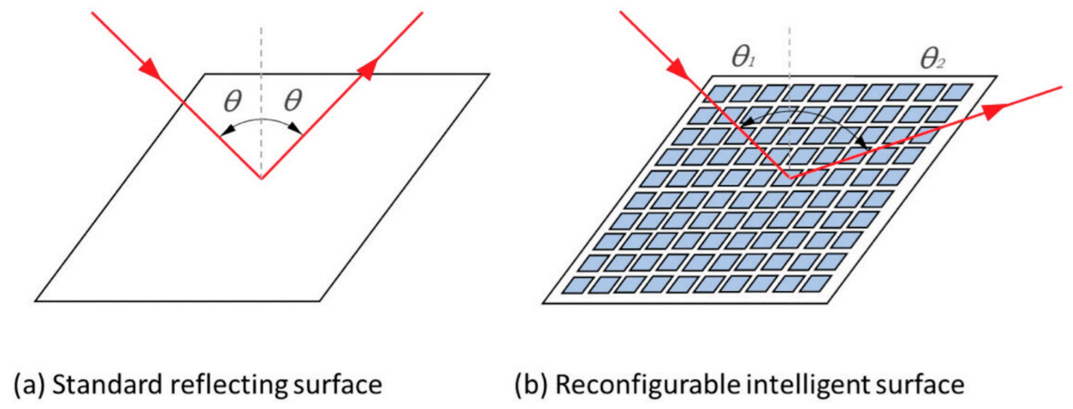
Microwave metamaterials, specifically programmable metasurfaces, can provide an innovative and energy-efficient solution to these emerging challenges. The goal is to “programme the wireless environment” through the use of reconfigurable intelligent surfaces (RIS), capable of redirecting a wireless signal, allowing it to travel around obstacles within the environment and refocus the faint signals gathered over a large surface precisely towards the target mobile device – significantly enhancing the signal strength in the process. A RIS comprises a number of repeating elements called unit cells or meta-atoms, each capable of steering and shaping the reflected or transmitted electromagnetic waves. A large number of these unit cells placed together within a surface allows RF beam steering, polarisation control and signal amplification to be achieved without the requirement of complex signal processing hardware – enabling operation with a close to zero power usage. Numerous RIS-enabled use cases have been identified [2,3,4,5] ranging from those providing not-spot coverage in urban or rural areas through to RIS-assisted physical layer security.
The development of RF and microwave metasurface technology has great potential for the current 5G wireless communications network and beyond. To date, wireless systems have been operated under the assumption that a wireless channel is intrinsically unpredictable. With the introduction of programmable metasurfaces[6], this long-standing view can be challenged, revolutionising the way future generations of wireless communications networks are designed and implemented. The objective is that reconfigurable metasurfaces will provide greater coverage, connectivity and spectral efficiency across the wireless network, particularly within urban and rural areas, whilst operating at a fraction of the energy consumption of current 5G wireless technologies.
Figure 1.
Basic operation of a reconfigurable intelligent surface [7].
- Current and Future Challenges
An RF metasurface can have a wired RF feed and act as a transmitter. If it has a wireless RF feed it can be RF passive or include RF amplification. It can operate in both reflection and transmission with paths having different RF feeds. The term RIS most commonly applies to an RF-passive surface operating in reflection. RIS face several fundamental technical challenges before they can be adopted for widespread use to shape the external electromagnetic environment:
- The computational complexity of RIS configuration grows rapidly with the number of unit cells and the number of end-users. As a RIS needs a large aperture to capture an incident RF beam and reduce diffraction at the edges, it can consist of thousands of unit cells. With increased number and mobility of end users, a high latency degrades beamforming and beamsteering performances. We propose further work is needed on the implementation of efficient RIS control algorithms to address the complexity/ latency/ performance trade-off.
- The basic RIS excludes sensing, so additional functionality is needed to localise users and estimate the channel state information, which adds further computational latency. We propose further work is needed to explore how sensing can be implemented within a RIS and the impact this could have on the complexity/ latency/ performance trade-off.
- When a mobile operator uses licensed spectrum, it is a licence condition to avoid interference in the adjacent frequency bands licensed to other operators. Out-of-band interference must be avoided in any multi-operator deployments. We propose further work is needed to design a unit cell response that only operates within tightly defined frequency bands.
- A RIS is designed to capture as much of the incident RF signal as possible and direct this to the estimated location of end-users. In a multi-user scenario with limited user co-scheduling, any users that are not in the estimated locations to which RF beams are steered will necessarily receive significantly reduced signal. By extension, since RIS is usually designed to be opaque and as reflective as possible, it will also necessarily shadow any users that are located behind it. We propose further work is needed on multi-functional surfaces [10] that minimise the impact of the RIS on users that are not interacting with the RIS.
- A RIS can be considered as a form of two-dimensional grating or as a diffraction pattern. As such, there will be a reflected main beam and also spurious reflected side lobes that will need to be minimised using a greater number of unit cells and more complex configurations. We propose further work is needed on RIS design to minimise spurious side-lobes.
- Integrating a RIS within a network as a new network component will need unique authentication, security, control data links and power supply. We propose further work is needed on the top-down system-level aspects of RIS operation, specifically addressing convergence between current standards-driven requirements (11,12,13] and the less mature technical demonstration [14–16].
- Advances in Science and Technology to Meet Challenges
These challenges can all be addressed with a variety of promising technical advances:
- If a RIS is to be used in a multi-operator location, out-of-band interference can be avoided by designing the unit cell resonant response to be narrowly confined within the licensed spectrum. Careful iteration of the metallisation pattern, diode placement, substrate layers and cell crosstalk is a time-consuming activity requiring EM Solver software and considerable patience.
- A RIS is certainly a low power device compared to a conventional 5G antenna array. Nevertheless, the PIN diodes or varactor used in the unit cell design need switching voltages to be controlled and then maintained, which consumes power. The RIS controller can itself also consume significant power so FPGA solutions are required to minimise power consumption.
- As an alternative or addition to purely electronic phase control using diodes in the unit cell, a RIS can use actuators to physically morph its shape, at both the unit cell level and also across the whole RIS. This can augment the range of electronic phase control, reduce the power consumption when the RIS is in a fixed configuration and also enable a conformal surface.
- Numerous physical mechanisms can be used to switch the phase response of a RIS. A RIS does not necessarily need to use diode-based electronic control. Electrically controlled surfaces can be switched very fast but tend to be lossy. Mechanically controlled surfaces tend to be slow to reconfigure. Optically controlled surfaces[8] offer the potential to switch rapidly with low loss and so could be good solutions where high-speed user tracking is required.
- A holographic antenna can be produced by placing surface wave launchers on to a surface with an imposed diffraction pattern, thereby producing a directed leaky-wave antenna. This is effectively the RF-active counterpart of an RF-passive RIS, since both are based on a reconfigurable surface and produce steerable RF beams, either directly or indirectly. Passive and active metasurfaces can be used together to localise users and shape the local EM environment.
- Integrate Sensing and Communications (ISAC)[9] is a well-established radar technique that can be adapted to RIS to permit user localisation and channel state estimation necessary for accurate and high quality RF beamforming and steering. Ideally both communications and sensing will occur in the same licensed frequency band but different frequency bands can also be used for a simpler implementation.
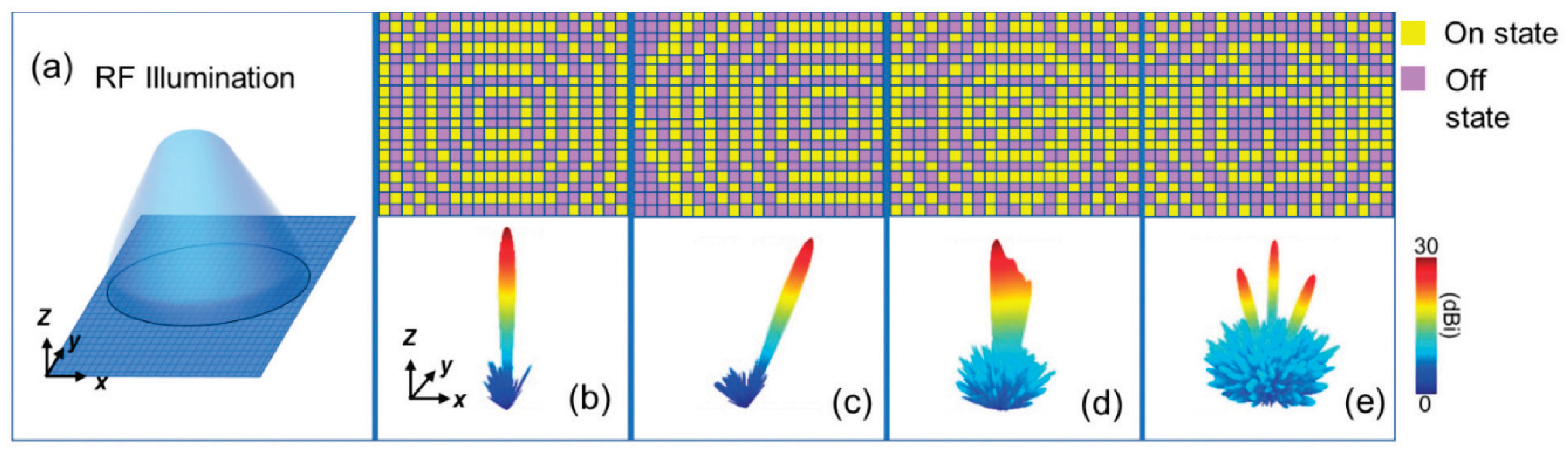
Figure 2.
Demonstration of unit cell state configurations and the resulting beam steering pattern[7].
Figure 2.
Demonstration of unit cell state configurations and the resulting beam steering pattern[7].
- Concluding Remarks
Programmable RF metasurfaces are now commonly called Reconfigurable Intelligent Surfaces (RIS) within the telecoms industry. A RIS is RF-passive and a holographic antenna is the RF-active counterpart. Programmable RF metasurfaces offer the ability to optimise the physical layer of mobile communications beyond 5G. A dominant physical layer challenge that current wireless networks face is the uncontrolled natural environment which dictates the reflection and scattering of radio waves. The physical world is dynamic and complex so the wireless channel between transmitter and receiver distorts a signal in non-trivial ways. Historically, mitigating hostile channel conditions can only be performed at the transmitter-side and receiver-side. With the advent of metasurfaces, wireless sensing and a new generation of artificial intelligence (AI), future mobile telecom networks have the potential to provide greater data throughput, improved coverage and improved energy efficiency.
Currently the two highest priorities to accelerate commercialisation are to address the complexity/ latency/ performance trade-off and to drive standards to consider top-down system-level aspects of RIS operation.
- Acknowledgements
The authors thank our collaborators at the University of Nottingham, University of Surrey, University of Warwick, University of Glasgow and the Horizon Europe INTEGRATE project for many useful discussions.
- References
- [1]
- Joseph Johnson et al. Global digital population as of January 2021. Stastica. Available at: www.statista.com/statistics/617136/digital-population-worldwide/
- [2]
- E. C. Strinati et al., "Wireless Environment as a Service Enabled by Reconfigurable Intelligent Surfaces: The RISE-6G Perspective," 2021 Joint European Conference on Networks and Communications & 6G Summit (EuCNC/6GSummit),Porto,Portugal,2021,pp.562-567,doi: 10.1109/EuCNC/6GSummit51104.2021.9482474.
- [3]
- Y. Zhang et al., "Smart Wireless Environment Enhanced Telecommunications: An Industrial Review on Network Stabilization," in IEEE Network, vol. 39, no. 1, pp. 21-29, Jan. 2025, doi: 10.1109/MNET.2024.3484573.
- [4]
- Abdalla, Aly Sabri, Talha Faizur Rahman, and Vuk Marojevic. "UAVs with reconfigurable intelligent surfaces: Applications, challenges, and opportunities." arXiv preprint arXiv:2012.04775 (2020).
- [5]
- Kisseleff, Steven, et al. "Reconfigurable intelligent surfaces for smart cities: Research challenges and opportunities." IEEE Open Journal of the Communications Society 1 (2020): 1781-1797.
- [6]
- Tang, Wankai, et al. "Wireless communications with programmable metasurface: New paradigms, opportunities, and challenges on transceiver design." IEEE Wireless Communications 27.2 (2020): 180-187.
- [7]
- A. Walker “Smart Surfaces for 5G and Beyond”. Journal of the Institute of Telecommunications Professionals. Vol 16, part 4, pp. 31-35. Dec 2022.
- [8]
- Kuznetsov, Arseniy I., et al. "Roadmap for optical metasurfaces." ACS photonics 11.3 (2024): 816-865.
- [9]
- Lu, Shihang, et al. "Integrated sensing and communications: Recent advances and ten open challenges." IEEE Internet of Things Journal 11.11 (2024): 19094-19120.
- [10]
- Tishchenko, A, et al. “The Emergence of Multi-Functional and Hybrid Reconfigurable Intelligent Surfaces for Integrated Sensing and Communications - A Survey” IEEE Communications surveys and tutorials, Vol.Early Access 08/01/2025
- [11]
- ETSI GR RIS 001: Reconfigurable Intelligent Surfaces (RIS): Use Cases, Deployment Scenarios and Requirements;
- [12]
- ETSI GR RIS 002: Reconfigurable Intelligent Surfaces (RIS): Technological challenges, architecture and impact on standardization;
- [13]
- ETSI GR RIS 003: Reconfigurable Intelligent Surfaces (RIS); Communication Models, Channel Models, Channel Estimation and Evaluation Methodology.
- [14]
- M. Di Renzo et al. “Smart Radio Environments Empowered by Reconfigurable Intelligent Surfaces: How It Works, State of Research, and The Road Ahead”. IEEE Journal on Selected Areas in communications. Vol. 38 (11). Nov. 2020.
- [15]
- X. Pei et al. “RIS-Aided Wireless communications: Prototyping, Adaptive Beamforming and Indoor/Outdoor field Trials”. IEEE Transactions on communications. Dec. 2021
- [16]
- T. Chen et al., "Model-Free Optimization and Experimental Validation of RIS-Assisted Wireless Communications Under Rich Multipath Fading," in IEEE Wireless Communications Letters, vol. 13, no. 3, pp. 627-631, March 202
3. Reconfigurable Intelligent Surfaces for Enhanced Radio Coverage in Wireless Communications and Healthcare Applications
Qammer H. Abbasi, Jalil ur Rehman Kazim, Farooq A. Tahir, Muhammad Ali Imran
James Watt School of Engineering, University of Glasgow, Glasgow, UK.
[qammer.abbasi@glasgow.ac.uk, jalil.kazim@glasgow.ac.uk, farooq.tahir@glasgow.ac.uk, Muhammad.imran@glasgow.ac.uk]
- Status
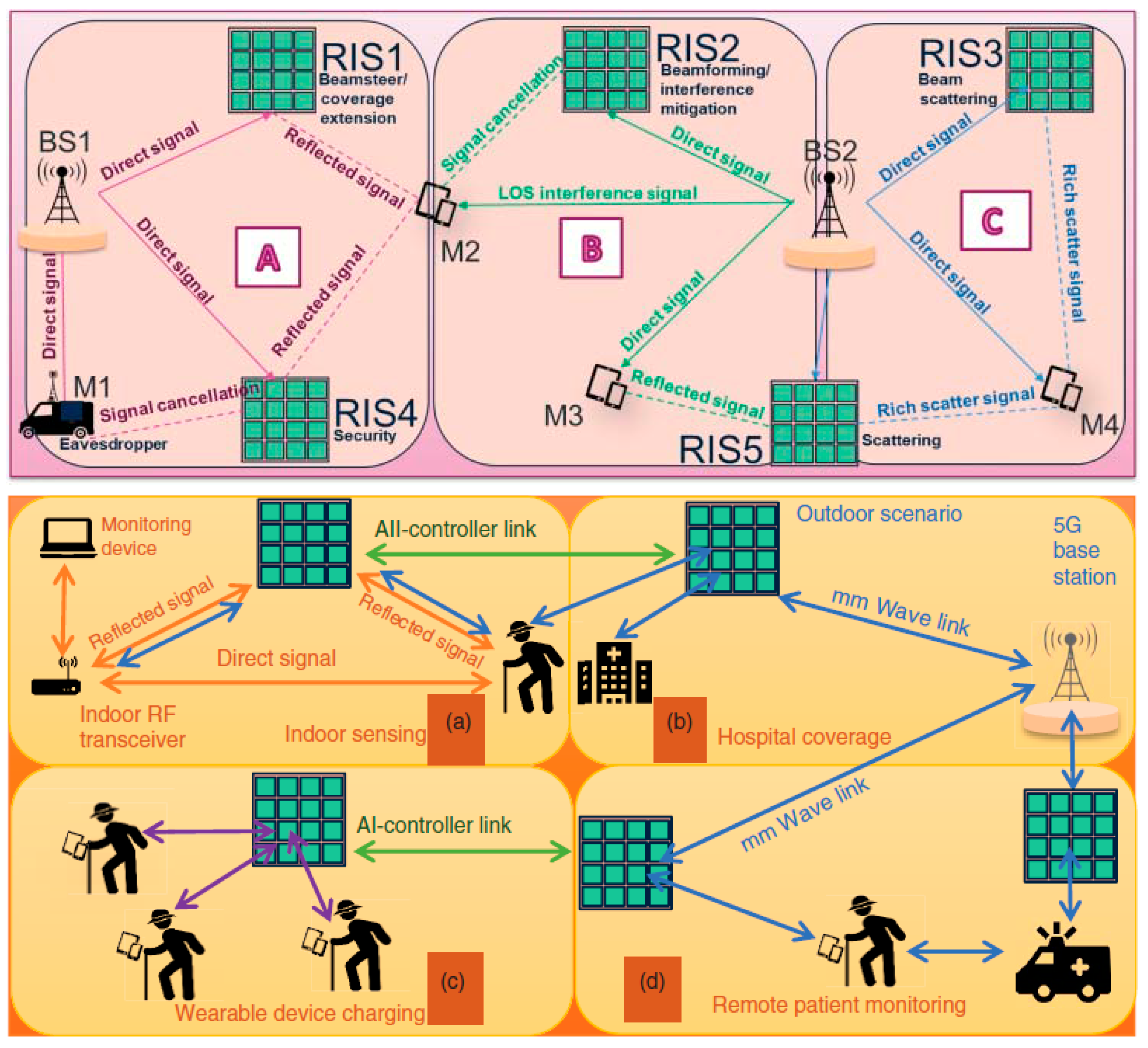
Reconfigurable Intelligent Surfaces (RIS) represent a transformative technology poised to revolutionize wireless communication and healthcare sectors. The concept of RIS emerged from the need to address the limitations of traditional wireless communication systems, such as signal attenuation, interference, coverage limitations, and spectrum scarcity [1]. By intelligently controlling the propagation environment, RIS offers exceptional prospects for enhancing wireless communication and healthcare applications. Figure 1 illustrates various deployment scenarios of RIS within both wireless communication and healthcare contexts [2]. The history of RIS traces back to seminal research in metamaterials and metamaterial-based structures in the early 2000s. Metamaterials are engineered materials with properties not found in nature, laid the foundation for developing surfaces capable of manipulating electromagnetic waves. Over the years, advancements in materials science, signal processing, and communication theory have accelerated the development of RIS technology. The RIS consists of a planar array of programmable elements distributed over a surface. These elements can dynamically adjust their properties to reflect, transmit, or absorb incoming electromagnetic waves, thereby optimizing signal strength, reducing interference, and improving communication reliability [3].
With respect to wireless communication, RIS can mitigate multipath fading, extend coverage to remote areas, and enable uniform connectivity in dense urban environments. Moreover, RIS-enabled communication systems can adapt to dynamic channel conditions, offering superior performance compared to traditional fixed infrastructure. For instance, RIS has proven to significantly boost the indoor wireless signal strength up to 40 dB with RIS deployed in three different scenarios [4]. Likewise, in outdoor urban settings, RIS integration into 5G networks has been shown to boost MIMO channel gains by 10 to 15 dB and has the potential to increase channel capacity by up to 50%, marking a substantial leap in network performance [5].
Transitioning to healthcare applications, RIS leverages existing RF signals for sensing, offering a non-invasive, privacy-respecting solution to monitor broad activities and human vitals. The advent of RIS considerably boosts this capability by enhancing Signal-to-Noise Ratios (SNR) and minimizing interference. This leap in technology enables precise monitoring of both macro [6] and micro movements such as heart rate [7], paving the way for smarter living and healthcare environments. Additionally, by integrating RIS alongside the wearable or implantable devices, healthcare practitioners can achieve precise localization and targeting of therapeutic signals.
This chapter uniquely highlights the dual impact of RIS in both wireless communication and healthcare—drawing on new experimental studies and real-world trials—to offer a practical perspective on future deployment, integration, and transformative applications.
Figure 1.
RIS deployment in different scenarios: (a) Wireless Communication (b) Healthcare. [2].
- Current and Future Challenges
Despite significant progress, the field of RIS faces several challenges that force further research and development. These include optimizing RIS design for real-world deployment, developing efficient algorithms for dynamic reconfiguration serving diverse applications simultaneously, miniaturization and scalability will enable their integration into smaller devices and systems, and addressing regulatory and standardization issues [8]. Further advances in RIS technology promise to unlock a myriad of benefits across various domains.
A critical aspect of RIS research is system integration. Integrating these surfaces into existing wireless communication and healthcare systems presents technical hurdles. Researchers are working to develop a framework to ensure compatibility and interoperability with different devices and networks. The absence of clear standards for RIS control interfaces, performance metrics, and interoperability with current wireless protocols continues to hinder wide adoption [9]. Overcoming these challenges is essential for the widespread adoption of RIS technology and its successful implementation in real-world applications. Advanced signal processing algorithms play a vital role in optimizing RIS performance in dynamic environments. Current research focuses on developing intelligent algorithms for tasks such as beamforming, interference mitigation, and resource allocation [10,11]. These algorithms are instrumental in enhancing communication reliability and efficiency by dynamically adjusting RIS configurations based on changing environmental conditions and user requirements. In healthcare applications, extending the use of RIS requires addressing specific challenges related to safety, reliability, and regulatory compliance. Researchers are working to validate the effectiveness of these surfaces in diagnostic imaging, therapeutic interventions, and patient monitoring. Ensuring privacy and data security is paramount, especially in healthcare. Beyond conventional encryption, RIS can enhance physical-layer security—for example, by dynamically shaping beams to prevent eavesdropping and jamming, as highlighted in recent studies on RIS-assisted physical-layer security in integrated sensing and communication systems [12].
Researchers are also confronted with the daunting task of enabling dynamic adaptation. Developing surfaces capable of autonomously adjusting to changing environmental conditions and user requirements represents a significant challenge. Future endeavours will concentrate on designing self-learning systems that can optimize performance in real-time without requiring human intervention. By creating adaptive mechanisms within RIS, researchers aim to enhance their flexibility and responsiveness, thereby maximizing their utility in diverse applications. Energy efficiency also stands as a crucial concern for the sustainable deployment of RIS in both wireless communication and healthcare systems [13]. Future research endeavours will seek into exploring various energy harvesting techniques, low-power circuit designs, and energy-aware algorithms. These efforts aim to minimize power consumption while preserving performance, ensuring that RIS can operate efficiently within resource-constrained environments without compromising functionality.
- Advances in Science and Technology to Meet Challenges
Advancements in material science can revolutionize the capabilities of RIS. Breakthroughs in this field will led to the development of novel materials with precisely tailored electromagnetic properties [14]. Emerging materials for RIS include flexible and transparent conductors, biocompatible dielectrics for healthcare, and printed metal inks for low-cost large-scale arrays. Recent work emphasizes the need to match materials and manufacturing to the specific application—be it urban deployment or medical monitoring. These materials empower RIS to manipulate electromagnetic waves across various frequencies and environmental conditions with unprecedented efficiency and effectiveness. Such advancements have opened new possibilities for RIS applications in wireless communication and healthcare, offering enhanced performance and versatility. Integration technologies play a decisive role in incorporating RIS into existing wireless communication and healthcare systems. Advances in integration techniques—including advanced packaging, thin-film deposition, and PCB-level integration—allow for compact, high-performance RIS suitable for mass deployment in wireless and healthcare applications. These technologies enable RIS to adapt to the specific requirements of different environments and applications, ensuring optimal performance and compatibility [15].
Continuous advancements in signal processing algorithms significantly enhance the performance of RIS in dynamic environments. Intelligent algorithms for beamforming, interference mitigation, and resource allocation enable RIS to adapt rapidly to changing conditions, optimizing communication reliability and efficiency [16]. These advancements ensure that RIS can effectively manage complex signal environments, delivering consistent and reliable performance across a range of scenarios. Innovations in energy-efficient design principles are essential for the sustainable deployment of RIS in wireless communication and healthcare systems. Through advancements in energy harvesting techniques, low-power circuitry, and energy-aware algorithms, RIS can minimize power consumption while maintaining optimal performance [17]. These developments extend the operation of RIS in resource-constrained environments, ensuring long-term viability and sustainability.
Ensuring robust security and privacy protection is paramount for the widespread adoption of RIS, particularly in sensitive applications like healthcare. State-of-the-art encryption, authentication, and access control mechanisms safeguard data transmitted and processed by RIS, mitigating cybersecurity risks and bolstering trust and confidence in the technology. Advanced cryptographic techniques and secure communication protocols are critical for maintaining the integrity and confidentiality of data in RIS applications.
- Concluding Remarks
In conclusion, reconfigurable intelligent surfaces represent a transformative technology with significant implications for wireless communication and healthcare. Through advancements in material science, integration technologies, signal processing algorithms, energy-efficient designs, security solutions, and scalable manufacturing processes, RIS offer extraordinary capabilities for manipulating electromagnetic waves and optimizing communication and healthcare systems. The potential of RIS to enhance communication reliability, efficiency, and coverage while enabling precise diagnostics, targeted therapies, and patient monitoring in healthcare settings is immense. As research and development efforts continue to address challenges and unlock the full potential of RIS technology, we can expect to see further innovation and transformation in wireless communication and healthcare, ultimately improving the quality of life for individuals worldwide.
- Acknowledgements
This work was supported by Engineering and Physical Sciences Research Council (EPSRC) grants: EP/X040518/1 and EP/T021020/1.
- References
- [1]
- Hassouna, S. et al. “A survey on reconfigurable intelligent surfaces : wireless communication perspective.” IET Communications, 17(5), pp. 497-537 (2023)
- [2]
- Kazim, Jalil ur Rehman, Abbas, Hasan T., Imran, Muhammad Ali, Abbasi, Qammer H., “Intelligent Reflective Surfaces – State of the Art,” pp. 1-18, 2021.
- [3]
- B. Rana, S. -S. Cho and I. -P. Hong, “Review Paper on Hardware of Reconfigurable Intelligent Surfaces,” in IEEE Access, vol. 11, pp. 29614-29634, 2023.
- [4]
- J. Rains et al., “High-Resolution Programmable Scattering for Wireless Coverage Enhancement: An Indoor Field Trial Campaign,” in IEEE Transactions on Antennas and Propagation, vol. 71, no. 1, pp. 518-530, Jan. 2023.
- [5]
- J. Rains, A. Tukmanov, Q. Abbasi, and M. Imran, “Experimental Insights into RIS-Enhanced MIMO Channels in Urban Environments,” arXiv preprint arXiv:2311.16985, 2023.
- [6]
- Usman, M., Rains, J., Cui, T.J. et al. Intelligent wireless walls for contactless in-home monitoring. Light Sci Appl 11, 212 (2022).
- [7]
- J. u. R. Kazim, A. Tahir, J. Rains, T. J. Cui, A. Jabbar, M. A. Jamshed, M. Ur-Rehman, A. Alomainy, M. A. Imran, and Q. H. Abbasi, “In-Home Monitoring Using Wireless on the Walls for Future HealthCare: Real-World Demonstration,” Advanced Intelligent Systems, vol. 5, no. 9, p. 2300007, 2023.
- [8]
- Syed, M.S.B.; Attaullah, H.M.; Ali, S.; Aslam, M.I. Wireless Communications beyond Antennas: The Role of Reconfigurable Intelligent Surfaces. Eng. Proc. 2023, 32, 10.
- [9]
- M. Åström, L. Pristagare, A. Ometov, and J. Markkula, “RIS in cellular networks—Challenges and issues,” arXiv preprint, arXiv:2404.04753, 2024.
- [10]
- M. M. Amri, N. M. Tran and K. W. Choi, “Reconfigurable Intelligent Surface-Aided Wireless Communications: Adaptive Beamforming and Experimental Validations,” in IEEE Access, vol. 9, pp. 147442-147457, 2021.
- [11]
- K. M. Faisal and W. Choi, “Machine Learning Approaches for Reconfigurable Intelligent Surfaces: A Survey,” in IEEE Access, vol. 10, pp. 27343-27367, 2022.
- [12]
- M. A. Shawky, S. T. Shah, Q. H. Abbasi, M. Hussein, M. A. Imran, S. F. Hasan, S. Ansari, and A. Taha, “RIS-enabled secret key generation for secured vehicular communication in the presence of denial-of-service attacks,” Sensors, vol. 23, no. 8, p. 4104, 2023.
- [13]
- C. Huang, A. Zappone, G. C. Alexandropoulos, M. Debbah and C. Yuen, “Reconfigurable Intelligent Surfaces for Energy Efficiency in Wireless Communication,” in IEEE Transactions on Wireless Communications, vol. 18, no. 8, pp. 4157-4170, Aug. 2019.
- [14]
- L. Zhang et al., “Active and programmable metasurfaces with semiconductor technologies,” Crystals, vol. 13, no. 2, p. 279, 2023
- [15]
- E. C. Strinati et al., “Reconfigurable, Intelligent, and Sustainable Wireless Environments for 6G Smart Connectivity,” in IEEE Communications Magazine, vol. 59, no. 10, pp. 99-105, October 2021.
- [16]
- C. Liaskos, S. Nie, A. Tsioliaridou, A. Pitsillides, S. Ioannidis and I. Akyildiz, “A New Wireless Communication Paradigm through Software-Controlled Metasurfaces,” in IEEE Communications Magazine, vol. 56, no. 9, pp. 162-169, Sept. 2018.
- [17]
- L. Zhao, Z. Wang and X. Wang, “Wireless Power Transfer Empowered by Reconfigurable Intelligent Surfaces,” in IEEE Systems Journal, vol. 15, no. 2, pp. 2121-2124, June 2021.
4. Designing for Manufacture
Milo Baraclough and Euan Humphreys
Defence Science and Technology Laboratory (mbaraclough@dstl.gov.uk; ehumphreys@dstl.gov.uk)
Content includes material subject to © Crown copyright (2024), Dstl. This material is licensed under the terms of the Open Government
Licence v3.0 except where otherwise stated. To view this licence, visit:
- Status
Many of us discovered when we first picked up a colour pencil that the concepts of our imagination were challenging to implement in reality. For a while this disappointment could be mitigated by the pure joy of casting colour across a page (experimentation), but the endeavour must, inevitably, be perfected and realised (exploitation) or discarded. In metamaterial design we encounter that same problem. The level of impact can vary significantly, but commonly a metamaterial that has been carefully designed and modelled for a specific performance fails to deliver those criteria when manufactured and measured. In circumstances when this occurs such work is published as proof of principle, but in order to progress beyond this stage to genuine application we must understand why these challenges occur in the transition from design to manufacture in order to overcome them.
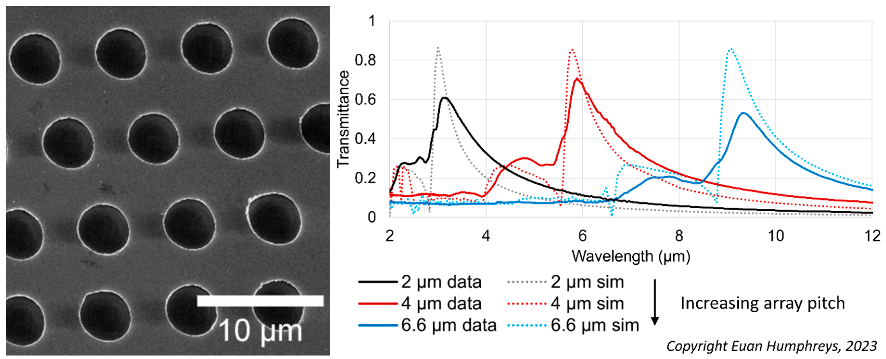
The finite tolerances of manufacturing techniques in real world scenarios are a frequent culprit for inconsistent performance between model and measurement (1; 2). Resonant metasurfaces that generate novel properties through the confinement of fields into small areas are inevitably susceptible to minute changes in the dimensions of those features, as can be seen in Figure 1. Minor deviations in the uniformity of the array results in a significant drop in transmission performance compared to predictions based on a perfect array. Deviation can also result from the material properties being inconsistent as was found by Z. Shen et al. (3), who designed a novel water-based negative refractive index metasurface that could be 3D printed. When manufactured, however, at least one resonance mode disappeared because the changing properties of the water with temperature could not be controlled in the model. M. Guo et al. (4) also found that slight variations in the refractive index of the constituent material of a 3D-printed metasurface absorber resulted in a change in its absorption of 6 decibels, which is a factor of 4 drop in absorbed power between prediction and measurement.
Figure 1.
(Left) SEM image of a laser-ablated hole array showing stitching errors, non-circular holes, and build-up of excess material. (Right) Plot of simulated vs measured transmittance of the pictured array. Performance drop is due to fabrication defects (13).
Figure 1.
(Left) SEM image of a laser-ablated hole array showing stitching errors, non-circular holes, and build-up of excess material. (Right) Plot of simulated vs measured transmittance of the pictured array. Performance drop is due to fabrication defects (13).
This high sensitivity to small variations also exacerbates the challenge of deriving the underlying physics of a metamaterial’s design, hindering our further understanding of complex interactions (5). In cases where the material is designed to be tuneable it is necessary to separate the uncertainty inherent in the manufacture from the material’s actively changing properties. None of these are unique problems for wireless metamaterials, or even metamaterials in general, but the class’s high reliance on periodicity and non-linear effects, along with their relatively small feature size, makes them highly vulnerable to these issues.
When a material is highly susceptible to small perturbations in manufacturing, it will also be sensitive to similar perturbations caused by damage in use. Outside of lab experimentation, in application sectors where assured performance is critical (such as aerospace, defence, emergency services etc.), any new material’s adoption will be predicated on being able to perform consistently from modelling to manufacture and under stress throughout its operational lifetime. Hence the interest in incorporating robustness into the design process from the beginning. For example, Tongtong et al. (Tongtong Zhang D. L., 2023) have demonstrated how using connected super units rather than the traditional single unit cell can greatly improve their material’s tolerance. By using a super unit of 16 interconnected unit cells, they can counteract the tolerance of their 3D printing technique, which produces visibly curved and irregular surfaces compared with the modelled design but has very good agreement in performance to simulation.
In the current status of wireless metamaterial development, the drive for more novel effects and exotic geometries leads to the use of small batch, experimental, manufacturing techniques or to push a design to the very edge of a given techniques functional tolerances. We propose that a roadmap for the future of wireless metamaterials include an awareness of the manufacturing challenges metamaterials face when attempting to reach wider adoption and that metamaterials be designed with these challenges in mind.
- Current and future challenges
- Designing for scale
In the lab it is possible to demonstrate a novel metamaterial response effectively enough for publication with a sample only a few wavelengths in diameter. At such scales a slow or inconsistent manufacturing technique can be a sensible choice. Making multiple samples until one is of acceptable quality, or waiting a few days for a process to finish, is acceptable in this context. When even moderate scale up is considered, however, these limitations can be intolerable.
Extraordinary optical transmission (EOT) array metasurfaces are made from a grid of holes in a thin plasmonic metal film, with transmission peak positions dependent on the hole spacing/pitch (7). EOT arrays can be fabricated directly via laser ablation, with the total time to make arrays covering the same area increasing as the hole size and spacing is scaled down. An example (8) that helps to quantify some of the effects of scaling on fabrication time shows 2×2 mm area arrays taking 3, 10 and 19 minutes to pattern 6.6, 4 and 2 µm pitch arrays respectively. EOT arrays have applications in biosensing where the existing standard is surface plasmon resonance sensors (9). EOT’s advantage over the existing technology, the ease with which it lends itself to miniaturisation, is directly undermined by the fact that it gets slower to make as feature density increases while the non-metamaterial (un-patterned) alternative has no such limitation.
For both large scale manufacture of metamaterials and bespoke creation of them in rapidly changing scenarios, a metamaterial needs to be accommodating to scale-up techniques in its design. Wet-etching for example can create a large, fine-featured area array in a very short time, but this requires the creation of etching masks and has additional material requirements and tolerances. Scaling up becomes even more challenging in the 3D space, with new technologies in that field bringing their own challenges.
- Designing for additive manufacture (AM)
Additive manufacture is an umbrella term for a range of 3D printing techniques and is a key technology for the rapid prototyping of metamaterial designs (10), allowing for both in house fabrication and access to designs that would otherwise be prohibitively expensive to outsource. It creates options for exploiting difficult/niche materials with limited commercial availability, seeing wide adoption and is an area of active study in its own right, providing ever increasing capability to metamaterial researchers. For all this, AM is not a universal solution. A metamaterial that is suitable for AM must be composed of materials that are compatible with the chosen manufacturing method, must have features of appropriate size for the materials and method, and must have performance that is robust within the dimensional tolerances of the manufacturing method and available hardware. For the most commonly used fabrication systems these tolerances can be around ~0.3% with a minimum tolerance of ±0.1 mm (11). Even if the tolerances could hypothetically be eliminated, 3D printing can also induce anisotropy. Existing simulation tools struggle to accommodate these limitations and realised performance suffers for it. This also limits the ability for previously demonstrate materials to be translated into a form suitable for AM.
AM technology is constantly improving and developing, the current limitations may one day be resolved as new techniques are created and existing ones refined, but a 3D printed metamaterial is unlikely to see wide adoption when it requires the mass deployment of cutting edge and expensive manufacturing tools. Better, then, if the design and fabrication philosophies of metamaterials adjust in step with manufacturing advances rather than designing for a future that may not come to pass. Doing this will help to accelerate the adoption of metamaterial enabled products in the market and lower the barriers to entry of metamaterial research.
- Advances in science and technology to meet the challenges
Designing for manufacture is a challenge best served by advances in simulation rather than more precise manufacture techniques. In this regard, one of the most compelling advances in is machine learning (12). Despite having significant potential to reduce design time and simplify optimisation, it has shortcomings that are yet to be fully explored, and in a research context brings the challenge of requiring dual expertise in both metamaterials and computer programming. If we resolve these challenges through inter-community collaboration, it is conceivable that a tool could be created that assesses a design’s robustness to a given tolerance, appropriateness for a manufacturing technique, or superfluous features that could be excluded to optimise manufacture speed.
Advances in manufacturing techniques (additive and conventional), including availability of a wider range of source materials for printing, advances in automation making rapid scale-up simpler and improvements to design tools for fabrication technology will all underpin future improvements for metamaterials and their exploitation. However, adopting design techniques and philosophies that allows the materials of tomorrow to be manufactured on the hardware of today will enhance the future impact of both near-term and far-future metamaterials without anchoring exploitation and adoption to an as yet unrealised technological advance.
- Concluding remarks
In conclusion, the field of metamaterials is over two decades old and has established a diverse and vibrant application space including novel optics, reconfigurable antennas, energy harvesting, exquisite sensing and more. If the extraordinary potential of this remarkable class of materials is going to continue to have the impact that the initial laboratory results have promised, a paradigm shift is required where metamaterial researchers consider, and design for, the challenges of manufacturing a material at scale reliably and repeatably. In doing so, they must make accommodations for how their modelled geometries might actually achieve functionality when deployed in a real-world setting. No matter the properties that future metamaterials could achieve, it is essential that the ongoing technology “push” is tempered with the end user and stakeholder requirements “pull” towards a mutually beneficial outcome.
This could be achieved through collaborative, cross domain, efforts linking researchers in manufacture and simulation to those in metamaterials. To achieve this, we propose co-located conferences on different topics with shared plenary sessions to raise awareness within existing communities without having to pass the hurdle of initiating a new one. These linked events should also encourage a sharing not just of results but practices, with design methods and simulation techniques given venues for presentation and publication. In order to broaden scope to those unable to attend conferences, publishers and funding bodies could be encouraged to accept proposals focusing on improving robustness and manufacturability through design and material selection over the existing pressure to produce novelty of effect. These tracks could be facilitated by industry sponsorship as both would result in designs with greater market readiness and in the development of dual complimentary skillsets for potential employees. Industry engagement with the UK Metamaterial Network is already positive and active; this roadmap could help give it a direction for a meaningful exploitation on a larger scale.
- References
- [1]
- Switchable 3D printed microwave metamaterial absorbers by mechanical rotation control. Chen, Kejian, et al. s.l. : IOP Publishing, 5 2020, Journal of Physics D: Applied Physics, Vol. 53, p. 305105.
- [2]
- Multi-material additive manufacture and microwave-assisted sintering of a metal/ceramic metamaterial antenna structure. Goulas, Athanasios, et al. 2023, Applied Materials Today, Vol. 33, p. 101878. ISSN: 2352-9407.
- [3]
- Design of negative refractive index metamaterial with water droplets using 3D-printing. Shen, Zhaoyang, et al. s.l. : IOP Publishing, 9 2017, Journal of Optics, Vol. 19, p. 115101.
- [4]
- 3D printed low-permittivity all-dielectric metamaterial for dual-band microwave absorption based on surface lattice resonances. Guo, Mengchao, et al. s.l. : IOP Publishing, 6 2022, Physica Scripta, Vol. 97, p. 075504.
- [5]
- Investigation of the coupling between tunable split-ring resonators. Baraclough, Milo, Hooper, Ian R. and Barnes, William L. 8, s.l. : American Physical Society, 8 2018, Phys. Rev. B, Vol. 98, p. 085146.
- [6]
- A multi-materials 3D-printed continuous conductive fibre-based metamaterial for broadband microwave absorption. Tongtong Zhang, Dichen Li, Zhen Yang, Yubing Duan, Ningyu Zhang, Ling Wang, Qingxuan Liang. 1, 2023, Virtual and Physical Prototyping, Vol. 19, p. e2285417.
- [7]
- Extraordinary optical transmission through sub-wavelength hole arrays. Ebbesen, Thomas W, et al. 1998, Nature, Vol. 391, pp. 667-669.
- [8]
- Single-Step Fabrication of High-Performance Extraordinary Transmission Plasmonic Metasurfaces Employing Ultrafast Lasers. de Galarreta, Carlota Ruiz, et al. 2, 2022, ACS Applied Materials & Interfaces, Vol. 14, pp. 3446-3454.
- [9]
- Surface plasmon resonance technology: Recent advances, applications and experimental cases. Davide Capelli, Viviana Scognamiglio, Roberta Montanari. 2023, TrAC Trends in Analytical Chemistry, Vol. 163, p. 117079.
- [10]
- 3D-printed Metamaterials with Versatile Functionalities. Lingling Wu, Jiacheng Xue, Xiaoyong Tian, Tengfei Liu, Dichen Li. 3, s.l. : Chinese Journal of Mechanical Engineering: Additive Manufacturing Frontiers, 2023, Vol. 2. 2772-6657.
- [11]
- Form Labs. Formlabs.com. [Online] Form Labs, May 05, 2023. [Cited: May 07, 2024.] https://formlabs.com/uk/blog/understanding-accuracy-precision-tolerance-in-3d-printing/.
- [12]
- Unleashing the Power of Artificial Intelligence in Materials Design. Badini, Silvia, Regondi, Stefano and Pugliese, Raffaele. 17, Switzerland : s.n., 8 2023, Materials (Basel, Switzerland), Vol. 16.
- [13]
- Humphreys, Euan. Active Extraordinary Optical Transmission Metasurfaces Using Phase-Change Materials. Exeter : University of Exeter, 2023.
5. THz Metamaterials for Beam Manipulation in Wireless Systems and Devices
Miguel Navarro-Cía
School of Physics and Astronomy, University of Birmingham (m.navarro-cia@bham.ac.uk )
- Status
TeraHertz (THz), the frequency window sandwiched between microwaves and infrared, is attracting a lot of interest driven by the promise of unprecented wireless capacity, high sensitivity to water, intermolecular bonds/motions, and carrier dynamics in semiconductors, and hyperspectral imaging with millimetre resolution even through many optically opaque materials [1]. All these features are well-suited for communication and sensing applications. In fact, the THz band unleashes joint communication and sensing opportunities that are being articulated in the definition of 6G [2]: benefited by the Tbps data rates promised by THz frequencies, 6G is expected to support high-definition holography and enable ultra-high-capacity wireless backhaul; meanwhile, benefited by THz’s fingerprinting potential and spatial resolution, 6G is expected to support unprecedented resolution radar and localisation, air quality monitoring, and nano-bio-sensing for transformative healthcare applications.
Metamaterials and their two-dimensional (2D) equivalent metasurfaces are and will play an important role in this context [3] as the manipulation of THz electromagnetic fields is not trivial due to two reasons: (i) the range of accessible material properties is rather limited at THz frequencies [4]; we have basically dielectrics (with moderate values of permittivity, except for few inorganic crystals, and in most cases lossy) and metals; there are no natural low-loss magnetics, not to speak about more exotic and interesting media such as chiral ones that an engineer would need in designing high-performance devices; (ii) THz beam diameters are only moderately large when measured in wavelengths and optical components for beam manipulation (e.g., lenses, mirrors, etc.) have also sizes comparable to the wavelength where diffraction phenomena is relevant [5].
Within the metamaterials paradigm, it becomes possible to widen the material design opportunities. By tailoring the unit cell properties and optimising their arrangements, metamaterials/metasurfaces have produced, among other scarce material properties, chirality and negative refractive index at THz frequencies [6]. The accessibility to a wider material properties has enabled different functionalities with high performance such as filtering with low transmission out of band over several decades [7], negative group delay [8], absorption [9], wave front engineering [10,11], high surface wave confinement [12], anomalouos reflection [13], carpet cloaking [14], and holography [15,16]. In turn, all these functionalities have resulted into improved devices such as detectors [17,18], including a commercial camera by Hamamatsu Photonics, functional emitters [19], modulators with GHz range of reconfiguration speed [20], including spatial THz modulators [21], planar antennas [22], and biosensors [23].
- Current and future challenges
In the context of wireless systems and devices, the most pressing challenge facing THz metamaterials, and thus, reflective intelligent surfaces, is still high performance reconfigurability, which is needed to break the fundamental performance bottleneck caused by the “multiplicative fading” effect introduced by passive reflective intelligent surfaces [24] Over the last decade or so, several tuning mechanisms for reconfigurability have been investigated, including microelectromechanical systems, thermal, microfluidic, liquid crystals, phase change materials and 2D materials [25,26] and significant milestones have been achieved [11,16,20,21], but either tuning speed is slow for communication systems, or the metamaterial has a limited number of units cells – producing poor to moderate radiation performance [27] –, or display hysteresis – rendering the metamaterial impractical for applications beyond the lab –, or the power consumption is too large or the performance deteriorates rapidly with tuning complicating the separation of the uncertainty inherent in the manufacture from the material’s actively changing properties needed for the designing for manufacture approach.
Other challenges that need to be addressed sooner rather than later are related to fabrication and accurate modelling as alluded in Section 4 of this Roadmap as a general problem for any new technology. The multiscale manufacturing needs of THz metamaterials falls through the cracks of standard microwaves and optical technology manufacturing techniques: the μm topological features of THz metamaterials demands optical technology manufacturing, but the required device size in the range of cm is ill-advised for them. Meanwhile, the fabrication volume/footprint is within reach for microwaves technology manufacturing, but not their accuracy requirements. Hence, THz metamaterials urge very advanced and expensive fabrication techniques with relative low manufacturing yield and not suitable for mass production that prevent the wide spread of THz metamaterials technology. The solution to this problem has been to use metasurfaces that can be fabricated with the more accessible optical photolithography or even laser ablation. However, this is done at the expense of limiting functionalities. If there were a cost-effective fabrication technique that allowed 2.5D metamaterials, let alone 3D metamaterials, the number of functionalities that could be encoded in a single metamaterial would explode as demonstrated at microwaves [28]. The modelling challenge is related to three aspects: (i) the inherent multiscale characteristic of THz metamaterials/metasurfaces [29], (ii) the relevance of diffraction due to being in quasi-optic territory [5], and (iii) the increasing importance of surface roughness [30].
A future challenge that can be easily envisioned at this stage is related to integration. With few exceptions, THz metamaterials/metasurfaces are designed, tested and modelled as isolated elements. In integrated solutions, loading effects between nearby components will emerge and will have to be studied not only from the electromagnetic, but also from the electronic, thermal, and electromechanical point of view. The multiphysics analysis is largely unchartered territory for THz metamaterials.
- Advances in science and technology meet challenges
To tackle the fabrication challenge that, to some extent, affects the reconfigurability challenge, one should steer the attention to the fast-growing additive manufacturing. Micro laser sintering has demonstrated high performance for classical all-metallic devices operating up to 0.2 THz [31] and should be a viable solution for 2.5D/3D THz metamaterials if accuracy is pushed down to a single digit of µm and surface finish is improved. Two-photon polymerisation direct laser writing meet the stringent dimensional accuracy and surface finish requirements for 2.5D/3D THz metamaterials and has been successfully used with a THz low-loss photoresin [32]. However, the process requires a sintering stage that cause a reduction in volume of the printed structure of ∼45% that is not necessarily isotropic for complex geometries. Hence, there is a need to either understand and control precisely the shrinkage due to the sintering stage or remove the sintering stage completely by finding a new THz low loss photoresin that does not require it. In fact, the development of low-cost dielectric materials/substrates with lower loss at millimetre-wave frequencies is in the agenda of electronic material multinationals [33]. Another advancement that would be a step change for both micro laser sintering and two-photon polymerisation direct laser writing would be the possibility to produce metallo-dielectric metamaterials without extra fabrication steps or at least to have an accurate and seamlessly two-step process.
Advances in THz near-field characterisation is an avenue to meet the integration challenge [34,35]. The possibility to inspect the near-field of fabricated THz metamaterials not only would provide key information about the fabrication, but also about potential near-field effects that could be embedded in the design optimisation of the integrated solutions. The prototyping of integrated solutions, meanwhile, could be greatly benefited using multiphysics topological optimisation/machine learning [36] that are well-suited for scenarios with complex nonlinear interactions as those emerging in integrated solutions.
- Concluding remarks
THz metamaterials hold promise for beam manipulation in wireless systems and devices, but there are a number of challenges for them to thrive and become the technology of choice. These challenges are in most cases intertwined and involve a collective effort from material and microfabrication scientists, microscopists, physicists, electrical and electronic engineers, computer scientists and eventually system engineers. The future tasks that this roadmap contribution identifies for wireless/THz metamaterials to become the technology of choice are: (i) reconfigurability of cm and even dm size metasurfaces with μs modulation speed and low power consumption aligned with 6G vision and global green agenda; (ii) multiphysics and multiscale designing for manufacture; (iii) development of low-cost dielectric materials for 2.5D/3D metamaterials with lower loss at millimetre-wave frequencies than those currently commercially available; and (iv) development of a multimaterial (ideally, metals and dielectrics) process with μm tolerance and cm to dm manufacture size.
- Acknowledgements
The work was partially supported by The Royal Society (grant nos. IEC\NSFC\191104, IES\R1\241009).
- References
- [1]
- Carpintero G, García-Muñoz E, Hartnagel H, Preu S, Raisanen A 2015 Semiconductor TeraHertz Technology: Devices and Systems at Room Temperature Operation (Chichester: Wiley-IEEE Press)
- [2]
- Li O et al. 2021 Joint European Conference on Networks and Communications & 6G Summit (EuCNC/6G Summit), 544-549
- [3]
- Al-Naib I, Withayachumnankul W 2017 Recent Progress in Terahertz Metasurfaces J. Infrared Milli Terahz Waves 38 1067-1084
- [4]
- Naftaly M 2015 Terahertz Metrology (Norwood: Artech House)
- [5]
- Goldsmith P F 1998 Quasioptical Systems: Gaussian Beam Quasioptical Propogation and Applications (Hoboken: Wiley)
- [6]
- Zhang S, Park Y S, Li J, Lu X, Zhang W, Zhang X 2009 Negative Refractive Index in Chiral Metamaterials Phys. Rev. Lett. 102 023901
- [7]
- Kuznetsov S A, Navarro-Cía M, Kubarev V V, Gelfand A V, Beruete M, Campillo I, Sorolla M 2009 Regular and Anomalous Extraordinary Optical Transmission at the THz-gap Opt. Express 17 11730-11738
- [8]
- Navarro-Cía M, Beruete M, Falcone F, Sorolla M, Lomakin V 2011 Negative group delay through hole arrays Phys. Rev. B 84 075151-1-5
- [9]
- Watts C M, Liu X, Padilla W J 2012 Metamaterial Electromagnetic Wave Absorbers Adv. Mat. 24 OP98-OP120
- [10]
- Kuznetsov S A, Astafev M A, Beruete M, Navarro-Cía M 2015 Planar Holographic Metasurfaces for Terahertz Focusing Sci. Rep. 5 7738-1-8
- [11]
- Lan F, Wang L, Zeng H, Liang S, Song T, Liu W, Mazumder P, Yang Z, Zhang Y, Mittleman D M 2023 Real-time programmable metasurface for terahertz multifunctional wave front engineering Light: Sci. Appl. 12 191
- [12]
- Navarro-Cía M, Beruete M, Agrafiotis S, Falcone F, Sorolla M, Maier S A 2009 Broadband spoof plasmons and subwavelength electromagnetic energy confinement on ultrathin metafilms Opt. Express 17 18184-18195
- [13]
- Liang L et a. 2015 Anomalous Terahertz Reflection and Scattering by Flexible and Conformal Coding Metamaterials Adv. Opt. Mat. 3 1374-1380
- [14]
- Zhou F, Bao Y, Cao W, Stuart C T, Gu J, Zhang W, Sun C 2011 Hiding a Realistic Object Using a Broadband Terahertz Invisibility Cloak Sci. Rep. 1 78
- [15]
- Wang Q, Plum E, Yang Q, Zhang X, Xu Q, Xu Y, Han J, Zhang W 2018 Reflective chiral meta-holography: multiplexing holograms for circularly polarized waves Light: Sci. Appl. 7 25
- [16]
- Venkatesh S, Lu X, Saeidi H, Sengupta K 2020 A High-speed programmable and scalable terahertz holographic metasurface based on tiled CMOS chips Nature Electronics 3 785-793
- [17]
- Kuznetsov S A, Paulish A G, Navarro-Cía M, Arzhannikov A V 2016 Selective pyroelectric detection of millimetre waves using ultra-thin metasurface absorbers Sci. Rep. 6 21079-1-11
- [18]
- Siday T, Vabishchevich P P, Hale L, Harris C T, Luk T S, Reno J L, Brener I, Mitrofanov O 2019 Terahertz Detection with Perfectly-Absorbing Photoconductive Metasurface Nano Lett. 19 2888-2896
- [19]
- McDonnel C, Deng J, Sideris S, Ellenbogen T, Li G 2021 Functional THz emitters based on Pancharatnam-Berry phase nonlinear metasurfaces Nat. Comms 12 30
- [20]
- Degl’Innocenti R et al. 2022 Terahertz Metamaterial Optoelectronic Modulators with GHz Reconfiguration Speed IEEE Trans. THz Sci. Techn. 12 520-526
- [21]
- Watts C M, Shrekenhamer D, Montoya J, Lipworth G, Hunt J, Sleasman T, Krishna S, Smith D R, Padilla W J 2014 Terahertz Compressive Imaging with Metamaterial Spatial Light Modulators Nat. Photonics 8 605-609
- [22]
- González-Ovejero D, Jung-Kubiak C, Alonso-delPino M, Reck T, Chattopadhyay G 2017 11th European Conf. on Antennas and Propagation (EUCAP)
- [23]
- Nourinovin S, Rahman M M, Naftaly M, Philpott M P, Abbasi Q H, Alomainy A 2024 Highly Sensitive Terahertz Metasurface Based on Electromagnetically Induced Transparency-Like Resonance in Detection of Skin Cancer Cells IEEE Trans. Biomed. Eng. 71 2180-2188
- [24]
- Zhang Z, Dai L, Chen X, Liu C, Yang F, Schober R, Poor V H 2023 Active RIS vs. Passive RIS: Which Will Prevail in 6G? IEEE Trans. Comms. 71 1707-1725
- [25]
- Xu C, Ren Z, Wei J, Lee C 2022 Reconfigurable terahertz metamaterials: From fundamental principles to advanced 6G applications iScience 25 103799
- [26]
- Degl’Innocenti R, Lin H, Navarro-Cía M 2022 Recent progress in Terahertz metamaterial modulators Nanophoton. 11 1485-1514
- [27]
- Navarro-Cía M, Pacheco-Peña V, Kuznetsov S A, Beruete M 2018 Extraordinary THz Transmission with a Small Beam Spot: The Leaky Wave Mechanism Adv. Opt. Mat. 6, 1701312
- [28]
- Song K, Cao Y, Chen Q, Gong X, Ji R, Liu Y, Zhao X, Wang M, Navarro-Cía M, Zhao Q 2023 Frequency and Angle Multiplexed Metadevices with Multifunctional Polarization Modulation Adv. Funct. Mat. 33, 2305145
- [29]
- Minatti G, Caminita F, Martini E, Sabbadini M, Maci S 2016 Synthesis of Modulated-Metasurface Antennas With Amplitude, Phase, and Polarization Control IEEE Trans. Antennas Propag. 64 3907-3919
- [30]
- Freer S, Qing J, Penchev P, Dimov S, Hanham S. M., Navarro-Cía M 2024 Loss Characteristics of TeraHertz Surface Waves on Laser Micromachined Textured Metals IEEE Trans. Terahertz Sci. Techn. 14, 283-292
- [31]
- Skaik T, Hunyor P, Beardsley M, Wang H, Huggard P G, Wang Y 2024 CNC-Machined and 3D-Printed Metal G-band Diplexers for Earth Observation Applications IEEE Trans. Comp. Pack. Man Techn. 14 1071-1078
- [32]
- Magaway E J Y, Farahi Y, Hanham S M, Zhang Z J, Guaidía-Moreno A, Navarro-Cía M 2023 Silica Nanoparticle-based Photoresin for THz High-Resolution 3D Microfabrication by Two-Photon-Polymerization IEEE Trans. Terahertz Sci. Techn. 13 415-418
- [33]
- Shang X, Ausden L, Naftaly M, Ridler N, Feng D, Navarro-Cía M, Hales J, Premerlani R 2025 IEEE MTT-S International Microwave Symposium (IMS 2025)
- [34]
- Hale L L, Keller J, Siday T, Hermans R I, Haase J, Reno J L, Brener I, Scalari G, Faist J, Mitrofanov O 2020 Noninvasive Near-Field Spectroscopy of Single Subwavelength Complementary Resonators Laser Photon. Rev. 14 1900254
- [35]
- Magaway E J Y, Navarro-Cía M 2024 The potential of THz Microscopy for Non-Destructive Evaluation Applications J. Non Destruct. Test. & Eval. 21 23-32
- [36]
- Hadjiantoni N, Feng D, Navarro-Cía M, Hanham S M 2025 Topological Optimization Framework for the Automated Design of 3D Printable THz Lens Antennas IEEE J. Multiscale Multiphysics Comput. Tech. 10 218-226
6. Metasurfaces for Radar Cross Section Reduction
Mustafa K Taher Al-Nuaimi and William G Whittow
Loughborough University, UK (m.al-nuaimi@lboro.ac.uk, w.g.whittow@lboro.ac.uk)
- Status
Radar systems find numerous applications in both civil and military fields and reducing the radar-cross-section (RCS) of objects is an important issue. For example, air or maritime navigation surveillance radar can be disrupted by the presence of tall structures in their surveillance zone. A well-known example of this is wind turbines where the movement of the blades creates a Doppler shift. The effectiveness of driving assistance radar can be compromised by the presence of objects with high RCS in their field of vision. Very recently, satellites (civilian or military) can now be subject to unfriendly activities (anti-satellite fire for instance) made possible using radar for detection and localization. As radar capabilities advance, so must stealth technologies evolve to maintain their effectiveness. In a related area, there are also application opportunities to increase the RCS for example for drones, tall buildings, and to increase safety for driverless vehicles.
Metasurfaces, with their ability to manipulate electromagnetic waves at a subwavelength scale, have emerged as a groundbreaking technology in the realm of enhanced stealth applications and RCS reduction for both civil and military applications [1]. The history of metasurfaces dates back to the early 21st century when researchers began exploring the possibilities of artificially engineered materials to control the propagation of electromagnetic waves [2]. Over the years, metasurfaces have evolved from passive structures to actively tunable devices, enabling unprecedented control over the scattering and absorption of electromagnetic radiation [3]. A recent popular variation of metasurfaces includes reconfigurable intelligent surfaces (RIS) which typically have a narrow band behavior, and a very high conductivity is required to limit losses. Metasurfaces for RCS reduction are a different class of metasurface where the aim is to scatter the incoming waves in all directions. A wide bandwidth of operation can be achieved. For RCS reduction, the conductivity does not need to as high as for RIS. Therefore, inkjet and screen printing, as well as other manufacturing techniques are possible.
Figure 1.
(a) Impact of metasurface application on radar RCS of a Fighter Jet. The application of a metasurface results in a 10 dB reduction in RCS, leading to a significant 40% decrease in radar detection range. (b) Diffuse scattering under normal incidence using metasurface [4]. (c) Metasurface RCS reduction characteristics under oblique incidence up to 60o [4].
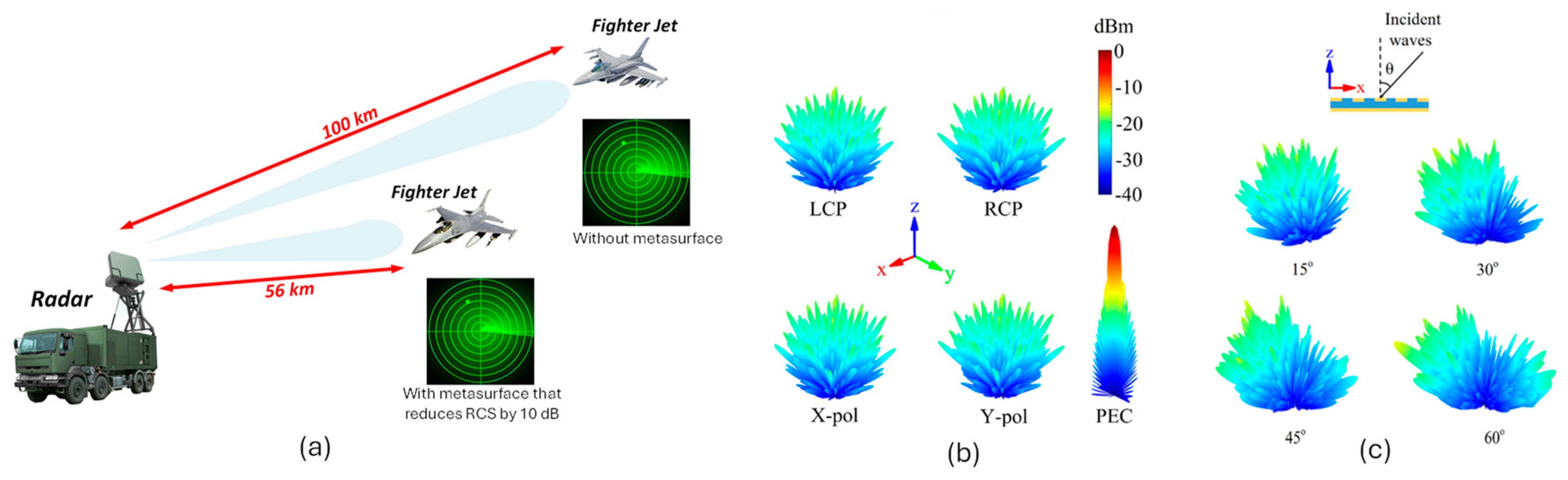
In the context of stealth technology, metasurfaces play a pivotal role in mitigating the detectability of objects by radar systems, thereby enhancing their stealth capabilities, see Figure 1(a). The importance of this field persists due to the continuous advancements in radar and sensing technologies, driving the need for more sophisticated and adaptable stealth solutions [4,5].
The ongoing research aims to develop metasurfaces that can dynamically adapt to different radar frequencies and polarizations, providing a versatile and responsive approach to stealth. Moreover, the integration of artificial intelligence and machine learning techniques into metasurface design is anticipated to yield self-optimizing structures capable of real-time adaptation to evolving threat scenarios. As metasurface research progresses, it is expected to unlock new dimensions in RCS control, allowing for not only reduced visibility but also controlled redirection of incident radar waves, see Figure 1(b)-(c). This will be particularly valuable in military and civilian applications where precise control over RCS is crucial. In conclusion, the history of metasurfaces reflects a journey from conceptualization to practical implementation, and their ongoing significance lies in their potential to revolutionize stealth capabilities through dynamic RCS modification. The pursuit of further advances in this field is imperative for staying at the forefront of modern technologies and ensuring the continued effectiveness of stealth applications in an ever-evolving threat landscape.
- Current and Future Challenges
Despite the promising advancements in metasurface technology for enhanced stealth applications and RCS modification, several challenges persist in the current research landscape, while new ones loom on the horizon. Existing metasurfaces typically perform optimally under narrow angles of incidence [6]. A significant obstacle in achieving broadband functionality lies in addressing wide-angles of incidence, specifically oblique incidence. Figure 1 (C) indicates that the RCS can be significantly reduced over wide angles of incidence of 60˚ [4]. However, there are challenges that remain in extending this performance to even wider angles. Overcoming this limitation necessitates the development of metasurface unit cells capable of dynamically adapting their electromagnetic (EM) characteristics to cover a broad range of incidence angles. This challenge calls for innovative and sophisticated design approaches for the unit cells that constitute the metasurface.
Metasurfaces can exhibit wider bandwidths than other classes of metasurfaces. This is evidenced by results in [1] that achieve greater than 10 dB of RCS reduction from 11 – 28 GHz (87% FBW) including angles up to 60˚; and similarly [5] covers 10 to 24 GHz including angles up to 60˚. Over this wide frequency bandwidth, no grating lobes were observed. However, extending this operational bandwidth in conjunction with extending the angles of incidence remains an ongoing challenge.
Novel and more efficient 2D destructive phase distributions, other than chessboard or random coding, that helps the unit cells to ensure angularly stable 10 dB of RCS reduction is also in need. Another pressing issue is the scalability of metasurface fabrication techniques. While laboratory-scale metasurface prototypes showcase remarkable capabilities, transitioning these technologies to practical (real-world), large-scale applications pose significant manufacturing challenges. The integration of metasurfaces into existing structures and materials also presents hurdles, requiring a balance between performance and compatibility.
Another pressing issue is, to date, almost all metasurfaces in the literature were designed and fabricated using stiff dielectric materials, which makes the integration of the metasurfaces on real-world objects impossible in some cases such as NASA almond structures. Thus, more material research should be conducted to produce a flexible and easy to bend (and perhaps transparent). Additionally, the susceptibility of metasurfaces to environmental factors, such as temperature variations and moisture, poses reliability concerns in real-world applications, necessitating robust and durable design solutions. Looking ahead, the incorporation of metasurfaces into complex three-dimensional structures, such as aircraft and vehicles, demands extensive research to address the associated engineering and integration challenges. Additionally, metasurfaces for RCS reduction should be low profile and lightweight, especially for applications in aerospace and defense. Achieving effective RCS reduction while minimizing the impact on the overall system weight and size is a critical consideration.
Understanding the long-term effects of metasurface deployment on the overall performance and structural integrity of these platforms is crucial for ensuring sustained effectiveness. As metasurface technology advances, ethical and regulatory considerations related to its application in military and civilian domains become increasingly pertinent. Striking a balance between innovation and responsible deployment will require collaborative efforts between researchers, policymakers, and industry stakeholders. In summary, while metasurfaces hold immense potential for revolutionizing stealth capabilities, addressing current challenges and anticipating future hurdles is essential to unlocking their full spectrum of applications in the realms of enhanced stealth and RCS modification.
- Advances in Science and Technology to Meet Challenges
In the pursuit of developing metasurfaces for RCS reduction, groundbreaking advances in science and technology are paramount to address the multifaceted challenges inherent in achieving optimal RCS reduction performance. One key area of advancement lies in the evolution of science and technology to fabricate flexible materials, see Figure 2. Conventional dielectric materials, often rigid and inflexible, pose inherent limitations in adapting to different shapes and structures required for optimal RCS reduction. The demand for metasurfaces with conformal and flexible properties has spurred significant advancements in material science and fabrication techniques.
Figure 2.
(a) Example of recently fabricated metasurface at Loughborough University using flexible materials. (b) RCS versus frequency curves of NASA Almond 3D geometry with/without metasurface [9]. (c) Conformal metasurfaces for RCS reduction [10].
Figure 2.
(a) Example of recently fabricated metasurface at Loughborough University using flexible materials. (b) RCS versus frequency curves of NASA Almond 3D geometry with/without metasurface [9]. (c) Conformal metasurfaces for RCS reduction [10].
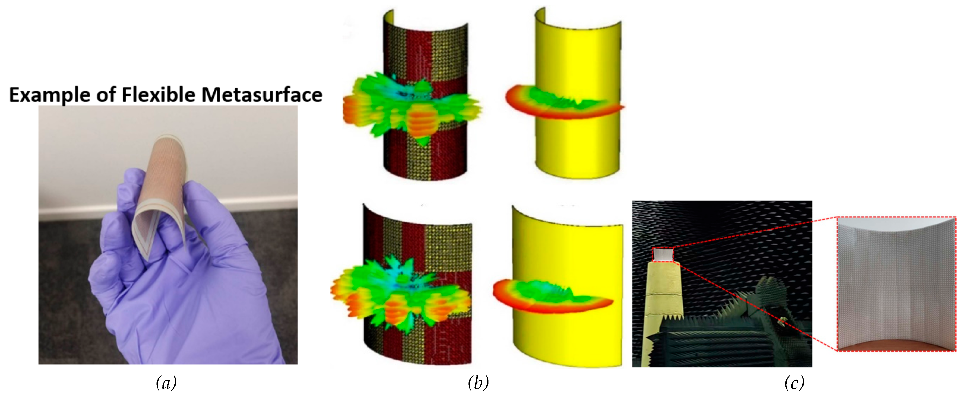
Novel materials, such as flexible polymers and elastomers, have emerged as promising candidates to replace rigid dielectric substrates. These materials offer the advantage of flexibility, allowing metasurfaces to conform to curved surfaces or irregular shapes, a critical requirement for stealth applications on diverse platforms. Advances in the synthesis of flexible materials involve tailoring their electromagnetic properties to ensure compatibility with radar frequencies of interest [7]. This includes engineering the dielectric constants, loss tangents, and other material parameters to achieve optimal absorption, reflection, or scattering characteristics for radar waves. Furthermore, the fabrication techniques for these flexible materials have undergone significant enhancements. Roll-to-roll manufacturing processes [8], for instance, enable the continuous production of flexible metasurface films over large areas, making them scalable for widespread applications. Additive manufacturing, including techniques such as 3D printing [9,10], allows for the creation of intricate and customized metasurface designs with precision, facilitating the realization of complex shapes that conform to the contours of the platforms they intend to conceal.
To address the challenges associated with wide-angle of incidence RCS reduction, researchers are leveraging computational methods and artificial intelligence (AI) algorithms to design the metasurfaces’ unit cells. Advanced simulations, utilizing high-performance computing, enable the optimization of metasurface designs for specific wide-angle of incidence. Machine learning algorithms are employed to analyze vast datasets, identifying optimal configurations of the unit cell and unit cell distribution that yield the highest stealth performance under widest angle of incidence. This integration of AI into the design process accelerates the development of metasurfaces with enhanced stealth capabilities. Furthermore, advancements in nanotechnology play a pivotal role in achieving finer control over the structure and properties of metasurfaces. Nanoscale fabrication techniques, such as electron beam lithography and focused ion beam milling, allow for the precise manufacturing of subwavelength structures on metasurfaces. These techniques enable the creation of metasurfaces with unique geometries and functionalities, contributing to improved stealth performance.
- Concluding Remarks
In conclusion, the exploration of metasurfaces for radar cross-section reduction represents a dynamic frontier in stealth technology, poised to reshape the landscape of modern military and civilian applications. The historical progression from conceptualization to active implementation underscores the evolving nature of metasurface research. The enduring significance of this field lies in its potential to revolutionize stealth capabilities through dynamic radar cross-section modification. Despite current challenges, the pursuit of flexible materials, advancements in artificial intelligence, and breakthroughs in nanotechnology hold the promise of overcoming existing limitations.
As we advance, collaborative efforts across disciplines, thoughtful ethical considerations, and proactive engagement with regulatory frameworks will be pivotal to ensuring the responsible deployment of metasurface technology. With ongoing research and technological innovation, metasurfaces stand as a cornerstone in the perpetual quest for staying ahead in the technological race between stealth technologies and radar systems, ensuring our ability to navigate an ever-evolving threat landscape with enhanced stealth and precision.
Future challenges include integrating these RCS-reducing metasurfaces into existing systems. This includes manufacturing over large conformal surfaces and complicated 3D shapes, and the material challenges to provide robust RF performance at high speeds or at high temperatures, without compromising the structural integrity. A further challenge is integrating these metasurfaces without compromising the existing communication capabilities.
- Acknowledgements
This work was supported by The Royal Society (UK) Newton Fellowship scheme under Grant NIF\R1\222093, and EPSRC grants TRANSMETA (EP/W037734/1) and ANISAT (EP/S030301/1).
- References
- [1]
- M. K. T. Al-Nuaimi, S. -L. Zhu, W. G. Whittow, G. -L. Huang, R. -S. Chen and Q. Shao, “Design of Polarization-Insensitive and Angularly Stable Metasurfaces With Symmetric Cubic Phase Distribution for Broadband RCS Reduction,” IEEE Transactions on Antennas and Propagation, vol. 72, issue 1, pp. 1069-1074, Jan. 2024.
- [2]
- P. Ball, “Bending the laws of optics with metamaterials: an interview with John Pendry,” National Science Review, vol. 5, Issue 2, pp. 200–202, March 2018.
- [3]
- N. I. Landy, S. Sajuyigbe, J. J. Mock, D. R. Smith and W. J. Padilla, “Perfect metamaterial absorber”, Phys. Rev. Lett., vol. 100, p. 207402, May 2008.
- [4]
- S. Zhao et al., “RCS reduction based on double parabolic phased metasurface,” Journal of Physics D: Applied Physics, vol. 56, pp. 435301-435311, 2023.
- [5]
- M. K. T. Al-Nuaimi, G. -L. Huang, W. G. Whittow, R. -S. Chen and S. -W. Wong, “Realization of Single-Layer Fourier Phased Metasurfaces for Wideband RCS Reduction,” IEEE Antennas and Wireless Propagation Letters, vol. 22, no. 5, pp. 1179-1183, May 2023.
- [6]
- A. Y. Modi, C. A. Balanis, C. R. Birtcher, and H. N. Shaman, “A New class of RCS-reduction metasurface based on scattering cancellation using array theory,” IEEE Transactions on Antennas and Propagation, vol. 67, no. 1, pp. 298–308, 2019.
- [7]
- P. Wang, “Multifunctional Graphene Metasurface for Highly Flexible Control of Microwave Absorption,” ACS Appl. Mater. Interfaces, vol. 16, issue 2, pp. 2649–2658, 2024.
- [8]
- S. Murthy, H. Pranov, N. A. Feidenhans’l, J. S. Madsen, P. E. Hansen, H. C. Pedersen and R. Taboryski, Plasmonic color metasurfaces fabricated by a high speed roll-to-roll method, Nano-scale, vol. 9, issue 37, pp. 14280-14287, 2017.
- [9]
- H. A. Khan et al., “A conformal coding metasurface for dual polarization conversion and radar cross section (RCS) reduction,” Journal of Optics, vol. 25, pp. 125102-125115, 2023.
- [10]
- Q. He et al., “Ultra-wideband and wide-angle RCS reduction of a concave structure based on a chessboard polarization conversion metasurfaces,” J. Phys. D: Appl. Phys. , vol. 57, pp. 035104-035113, 2024.
7. Wireless and Microwave Metasurfaces in Bioelectronics
Rupam Das
Electronic Engineering Department, University of Exeter (r.k.das@exteter.ac.uk)
- Status
Wireless technologies are essential for bioelectronic devices used in diagnostics and therapy, ranging from early pacemakers [1] to modern implants like cochlear [2] and retinal devices [3], health monitors, ingestible cameras [4], and spinal cord stimulators [5]. Historically, these devices have depended on batteries for power and reliability over their operational lifespan. However, challenges persist with batteries [6], including their bulkiness for high storage capacity and the need for replacement surgeries due to limited lifespans and corrosion.
Wireless power transfer (WPT) systems present a promising alternative to address these issues. WPT enables device miniaturization, reduces infection risks associated with surgical replacements, and ensures stable long-term operation through reliable wireless charging [7,8]. These advancements suggest that WPT can revolutionize implantable medical devices, enhancing patient outcomes and long-term usability. Radiofrequency (RF) techniques are the most prevalent wireless technology in bioelectronics due to their safety and maturity [9]. However, the human body’s lossy, heterogeneous, and dispersive nature poses challenges by absorbing electromagnetic radiation [10]. To avoid adverse effects, lower frequencies (below 5 GHz) are used, which limits miniaturization and the ability to focus electromagnetic fields [11]. Additionally, variations in body size, composition, and movement complicate the design of bioelectronic components.
Metasurfaces [12–14], which are structured at the subwavelength scale, offer innovative solutions. These flat, flexible devices can amplify or suppress electromagnetic interactions, enhancing performance and allowing integration into wearable and implantable devices. Metasurfaces can manipulate the amplitude, phase, and polarization of electromagnetic waves, reaching otherwise inaccessible physiological regions [15]. Flexible electronics, including energy harvesters [16] and smart skins [17], benefit from metasurface advancements, which offer improved performance and new capabilities, indicating a promising future for bioelectronics.
- Current and future challenges
Integrating metamaterials and metasurfaces into bioelectronics comes with several significant challenges. Firstly, designing and fabricating these materials for optimal performance in the complex biological environment is challenging due to the heterogeneous nature of biological tissues, which exhibit varying electromagnetic properties. Predicting and controlling electromagnetic wave behavior in such an environment requires advanced and often costly nanofabrication techniques. Moreover, ensuring that these metasurfaces maintain their functionality when scaled down for practical applications in wearable and implantable devices is a critical hurdle [18]. Biocompatibility and long-term stability of metasurfaces also pose major challenges. Bioelectronic devices must be safe for extended use within the human body, necessitating materials that do not provoke immune responses or degrade over time [19]. Additionally, integrating these materials into flexible and stretchable substrates suitable for biomedical devices requires ensuring that their mechanical properties match the flexibility and durability needed for continuous use [20].
Power efficiency and thermal management are significant concerns for metasurface-based bioelectronic devices. The human body has strict limits on the amount of electromagnetic energy that can be safely transmitted, restricting the operational power of these devices. Metasurfaces must be designed to minimize energy loss and manage heat dissipation effectively to avoid tissue damage. Future advancements need to focus on enhancing the energy efficiency of these devices while ensuring they operate within safe exposure thresholds to electromagnetic fields [10].
Looking forward, the integration of metasurfaces with advanced technologies like artificial intelligence (AI) and machine learning (ML) offers promising opportunities [21,22] but introduces new challenges. AI and ML can optimize the design and functionality of metasurfaces, enabling real-time adaptability and improved performance. However, embedding these sophisticated computational capabilities within bioelectronic devices requires developing new algorithms and computational models that can function efficiently on the limited hardware of wearable and implantable devices. Seamlessly integrating these advanced technologies with metasurfaces will be crucial for realizing their full potential in future bioelectronics.
- Advances in science and technology to meet challenges
To advance metasurface-based bioelectronics, innovation in circuit design, materials, and the use of AI for design optimization is crucial. Despite progress, achieving comprehensive electromagnetic control near the human body remains challenging, mainly due to the limited number of unit cells and tunability in current designs. Implementing novel control mechanisms, including mechanical actuation, optical control, and phase-change materials, offers potential for improving resolution and tunability [23].
For example, dynamic polarization control could address the challenges related to the variable orientation of bioelectronic devices on or within the body [24]. Although optical metasurfaces have explored these concepts, their application in bioelectronic wireless systems is still limited. Additionally, emerging nonlinear [25] and time-varying metasurfaces [26] could introduce novel functionalities, such as Doppler shifts and broken Lorentz reciprocity, potentially enhancing biosensor sensitivity and enabling efficient power transfer to mobile devices. Translating capabilities from optical to RF metasurfaces for bioelectronics involves distinct challenges, including material preferences and penetration depths within biological tissues. While metals with high conductivity are advantageous at radiofrequencies, optical frequencies favour dielectric materials due to lower losses [27]. Optical metasurfaces leverage light’s molecular selectivity for interactions with biological matter, whereas RF metasurfaces can penetrate deeper into tissues. Navigating these differences and leveraging scale-invariant principles from Maxwell’s equations presents opportunities and challenges in advancing metasurface applications for bioelectronics across both optical and RF domains [27].
Metasurfaces for bioelectronics must be flexible and stretchable to integrate with the human body [8,28,29]. Materials like polyimide, polyethylene terephthalate, ecoflex, polydimethylsiloxane, and textiles offer fabrication methods such as direct and transfer printing. Longer wavelengths reduce resolution demands. Rigid conductors like copper, gold, and aluminum can be made flexible through structural designs like serpentine lines [16], with necessary adjustments for inductance and capacitance. Flexible conductive materials like conductive polymers, hydrogels, and ionogels, such as PEDOT, are promising despite lower conductivity [28]. Liquid metals provide both flexibility and high conductivity for applications like microfluidic antennas [30]. Functional materials can transduce biochemical changes into electromagnetic responses. For example, hydrogels alter permittivity under pressure or sweat, enabling wireless detection [31]. Two-dimensional materials like graphene enable sensors sensitive to biological environments [32]. Biodegradable materials like magnesium, silk, and cellulose create transient metasurfaces [33], while self-healing materials enhance durability for wearable devices [34]. Another emerging trend is integrating transparency into these bioelectronics, which holds the potential to preserve and utilise visual information from interfacing biological systems [35]. This capability could significantly advance comprehensive clinical diagnosis through sophisticated image analysis techniques.
Furthermore, the future of bioelectronics holds significant promise with the advent of magnetoelectric (ME) antennas [36], which are poised to revolutionize the field through enhanced miniaturization and functionality. Traditional antennas rely on wavelengths that are often large relative to the size of the device, making it challenging to achieve the necessary compactness for integration into wearable and implantable bioelectronics. Magnetoelectric antennas, however, can achieve similar performance at a fraction of the size, allowing for the development of much smaller and more discreet bioelectronic devices. This miniaturization opens new possibilities for continuous health monitoring and seamless integration with the human body.
AI enables researchers to efficiently explore complex parameter spaces, aiding in the discovery of innovative metasurfaces. AI models for metasurface design22 can be categorized into supervised, unsupervised, or hybrid models. Generative models, including Generative Adversarial Networks (GANs) [21] and Variational Autoencoders (VAEs), create novel metasurface designs by exploring latent spaces and patterns that would be labor-intensive to identify manually. GANs are effective at generating structures and architectures, while VAEs can offer new configurations with specific functionalities. Optimization algorithms, such as genetic algorithms and particle swarm optimization, also play a crucial role. Genetic algorithms use natural selection principles, whereas particle swarm optimization leverages adaptation principles to fine-tune metasurface architecture. Generative models excel in creativity, producing novel concepts, while optimization algorithms focus on efficiency and finding optimal solutions. Model evaluation involves cross-comparison, performance indices, bootstrapping, and cross-validation to ensure accurate predictions and avoid overfitting.
- Concluding remarks
Due to their versatility and compact size, metasurfaces offer functionalities that conventional radio-wave components cannot achieve in biomedical applications. Metasurfaces excel in controlling electromagnetic waves precisely within and around the body, which is crucial for advancing connected personal healthcare systems. Recent advancements highlight their potential in integrating bioelectronics with the human body and designing devices for wireless health monitoring and therapy. However, additional testing is essential to validate their suitability for medical applications.
- References
- [1]
- Elmqvist, R. & Senning, A. An implantable pacemaker for the heart. In Proceedings of the Second International Conference on Medical Electronics, Paris (ed. Smyth, C. N.) 27 (Iliffe, 1959).
- [2]
- Zeng, F.-G., Rebscher, S., Harrison, W., Sun, X. & Feng, H. Cochlear implants: system design, integration, and evaluation. IEEE Rev. Biomed. Eng. 1, 115–142 (2008).
- [3]
- Weiland, J. D. & Humayun, M. S. Visual prosthesis. Proc. IEEE 96, 1076–1084 (2008).
- [4]
- Wu, G. & Xue, S. Portable preimpact fall detector with inertial sensors. IEEE Trans. Neural Syst. Rehabil. Eng. 16, 178–183 (2008).
- [5]
- Samineni, V. K. et al. Fully implantable, battery-free wireless optoelectronic devices for spinal optogenetics. Pain 158, 2108 (2017).
- [6]
- A. B. Amar, A. B. Kouki, H. Cao, “Power Approaches for Implantable Medical Devices”, Sensors , 15, 28889 (2015).
- [7]
- Won, S.M., Cai, L., Gutruf, P. et al. Wireless and battery-free technologies for neuroengineering. Nat. Biomed. Eng 7, 405–423 (2023).
- [8]
- R. Das, F. Moradi and H. Heidari, “Biointegrated and Wirelessly Powered Implantable Brain Devices: A Review,” in IEEE Transactions on Biomedical Circuits and Systems, vol. 14, no. 2, pp. 343-358 (2020).
- [9]
- Pozar, D. M. Microwave Engineering (Wiley, 2011).
- [10]
- Lin, J. C. A new IEEE standard for safety levels with respect to human exposure to radio-frequency radiation. IEEE Antennas Propag. Mag. 48, 157–159 (2006).
- [11]
- R. Das and H. Yoo, A Multiband Antenna Associating Wireless Monitoring and Nonleaky Wireless Power Transfer System for Biomedical Implants, in IEEE Transactions on Microwave Theory and Techniques, vol. 65, no. 7, pp. 2485-2495 (2017).
- [12]
- Zhang, L., Mei, S., Huang, K. & Qiu, C. W. Advances in full control of electromagnetic waves with metasurfaces. Adv. Opt. Mater. 4, 818–833 (2016).
- [13]
- Hu, Z., Liu, C., & Li, G. Disordered optical metasurfaces: from light manipulation to energy harvesting. Advances in Physics: X, 8(1), (2023).
- [14]
- Mao, P., Liu, C., Li, X. et al. Single-step-fabricated disordered metasurfaces for enhanced light extraction from LEDs. Light Sci Appl 10, 180 (2021).
- [15]
- Wu, K., Coquet, P., Wang, Q. J. & Genevet, P. Modelling of free-form conformal metasurfaces. Nat. Commun. 9, 3494 (2018).
- [16]
- R. Das, E. McGlynn, M. Yuan and H. Heidari, “Serpentine-Shaped Metamaterial Energy Harvester for Wearable and Implantable Medical Systems,” ISCAS, Daegu, Korea, pp. 1-5, (2021).
- [17]
- Xiong, W.; Zhu, C.; Guo, D.; Hou, C.; Yang, Z.; Xu, Z.; Qiu, L.; Yang, H.; Li, K.; Huang, Y. Bio-inspired, intelligent flexible sensing skin for multifunctional flying perception. Nano Energy, 90, 106550, (2021).
- [18]
- Gollub, J. et al. Large metasurface aperture for millimeter wave computational imaging at the human-scale. Sci. Rep. 7, 42650 (2017).
- [19]
- Yang, X., Zhou, T., Zwang, T.J. et al. Bioinspired neuron-like electronics. Nat. Mater. 18, 510–517 (2019).
- [20]
- Li, Z., Tian, X., Qiu, CW. et al. Metasurfaces for bioelectronics and healthcare. Nat Electron 4, 382–391 (2021).
- [21]
- Yunwei Mao et al., Designing complex architectured materials with generative adversarial networks. Sci. Adv.6,eaaz 4169(2020).
- [22]
- Ece Tezsezen, Defne Yigci, Abdollah Ahmadpour, and Savas Tasoglu, AI-Based Metamaterial Design, ACS Applied Materials & Interfaces, 16 (23) (2024).
- [23]
- Bao, L. & Cui, T. J. Tunable, reconfigurable, and programmable metamaterials. Microw. Opt. Technol. Lett. 62, 9–32 (2020).
- [24]
- Wang, S., Deng, ZL., Wang, Y. et al. Arbitrary polarization conversion dichroism metasurfaces for all-in-one full Poincaré sphere polarizers. Light Sci Appl 10, 24 (2021).
- [25]
- Almeida, E., Bitton, O. & Prior, Y. Nonlinear metamaterials for holography. Nat. Commun. 7, 12533 (2016).
- [26]
- Amr M. Shaltout et al., Spatiotemporal light control with active metasurfaces, Science, 364, eaat3100 (2019).
- [27]
- Glybovski, S. B., Tretyakov, S. A., Belov, P. A., Kivshar, Y. S. & Simovski, C. R. Metasurfaces: from microwaves to visible. Phys. Rep. 634, 1–72 (2016).
- [28]
- Ray, T. R. et al. Bio-integrated wearable systems: a comprehensive review. Chem. Rev. 119, 5461–5533 (2019).
- [29]
- Ee, H.-S. & Agarwal, R. Tunable metasurface and flat optical zoom lens on a stretchable substrate. Nano Lett. 16, 2818–2823 (2016).
- [30]
- Leber, A. et al. Soft and stretchable liquid metal transmission lines as distributed probes of multimodal deformations. Nat. Electron. 3, 316–326 (2020).
- [31]
- Dautta, M. et al. Multi-functional hydrogel-interlayer RF/NFC resonators as a versatile platform for passive and wireless biosensing. Adv. Electron. Mater. 6, 1901311 (2020).
- [32]
- Mannoor, M. S. et al. Graphene-based wireless bacteria detection on tooth enamel. Nat. Commun. 3, 763 (2012).
- [33]
- Lei, T. et al. Biocompatible and totally disintegrable semiconducting polymer for ultrathin and ultralightweight transient electronics. Proc. Natl Acad. Sci. USA 114, 5107–5112 (2017).
- [34]
- Cao, Y. et al. Self-healing electronic skins for aquatic environments. Nat. Electron. 2, 75–82 (2019).
- [35]
- Cho, Y.U., Lim, S.L., Hong, JH. et al. Transparent neural implantable devices: a comprehensive review of challenges and progress. npj Flex Electron 6, 53 (2022).
- [36]
- Zaeimbashi, M., Nasrollahpour, M., Khalifa, A. et al. Ultra-compact dual-band smart NEMS magnetoelectric antennas for simultaneous wireless energy harvesting and magnetic field sensing. Nat Commun 12, 3141 (2021).
8. Flexible Antennas and Metasurfaces for Future Millimeter-wave Beyond 5G Communication
Anikó Német1, Syeda Fizzah Jilani1, Muhammad Aslam2
1Department of Physics, Aberystwyth University, UK, SY23 3BZ (ann23@aber.ac.uk, sfj7@aber.ac.uk)
2Department of Computer Science, Aberystwyth University, UK, SY23 3DB (mua19@aber.ac.uk)
- Status
Flexible antennas and metasurfaces are key players on the Internet of Everything (IoE) beyond 5G wireless applications. The increasing number of user-friendly wireless devices contributes greatly towards modern lifestyles by transforming how people work, communicate, and interact with the modern world. Smart wearables are vital in real-time health monitoring and diagnostics, augmented and virtual reality AR/VR experiences, smart textiles, enhanced connectivity, smarter human-machine interaction, security and surveillance, and provide sustainable solutions across industries [1]. While a surge of research in compact, flexible and wearable 5G antennas has gained massive success, the extensive adoption of these technologies across diverse internet-of-things (IoT) applications is still evolving. Significant deployment is done in health monitoring wearables, and smart clothing for military and firefighter garments, however, large-scale integration into everyday applications like smart agriculture, smart homes, and industrial technologies is in progress. Figure 1 shows the scope of wearable antennas and metasurfaces beyond 5G/6G applications.
Research into biodegradable materials for electronics is crucial in reducing the electronic waste (e-waste) and environmental impact of these systems [2]. The global e-waste generation reached 53.6 million metric tons in 2019, the world generated a striking 53.6 Mt of e-waste, an average of 7.3 kg per capita, and is projected to grow to 74.7 Mt by 2030 [3,4]. Advances in material science, such as biocompatible conductors, biopolymers, and cellulose-based materials can be used in developing biodegradable antennas and printed metasurfaces for seamless wireless connectivity and biodegradability, leaving no harmful residue to the environment. Recently, research on using carbon-based materials like graphene and carbon nanotubes in flexible antennas and metasurfaces has received attention due to their low profile, light weight, low cost, high resistance to corrosion, thermal stability, and tunable conductivity. These new materials exhibit remarkable properties that make them highly attractive for future eco-friendly applications, particularly for millimeter-wave (mm-wave) and terahertz (THz) communications. Several advanced manufacturing techniques have recently been developed to ensure fabrication consistency, reliability, cost-effectiveness and accuracy for biodegradable antennas and printed metasurfaces.
Flexible metasurfaces, in particular, are increasingly recognized as transformative enablers for next-generation communications. Unlike conventional antennas, metasurfaces provide unprecedented control of electromagnetic (EM) wavefronts, enabling beam steering, focusing, holography, and reconfigurable wireless environments that can dynamically adapt to user needs [10–12]. Recent experimental demonstrations have validated the use of reconfigurable intelligent surfaces (RIS), a class of metasurfaces, for extending coverage, improving spectral efficiency, and reducing energy consumption in beyond 5G networks [13,14]. Moreover, the integration of flexible and conformal metasurfaces into wearables opens new possibilities for body-centric wireless networks, immersive AR/VR connectivity, and in-body biomedical communications [15]. This distinguishes metasurfaces from traditional flexible antennas by providing a multifunctional and adaptive communication layer essential for the IoE ecosystem.
Figure 1.
Potential applications of flexible antennas and metasurfaces beyond 5G/6G, including smart wearables, AR/VR, biomedical implants, and IoE environments. Reconfigurable metasurfaces can enable low-power beamforming, electromagnetic cloaking for privacy/security, and energy-efficient signal routing across these domains.
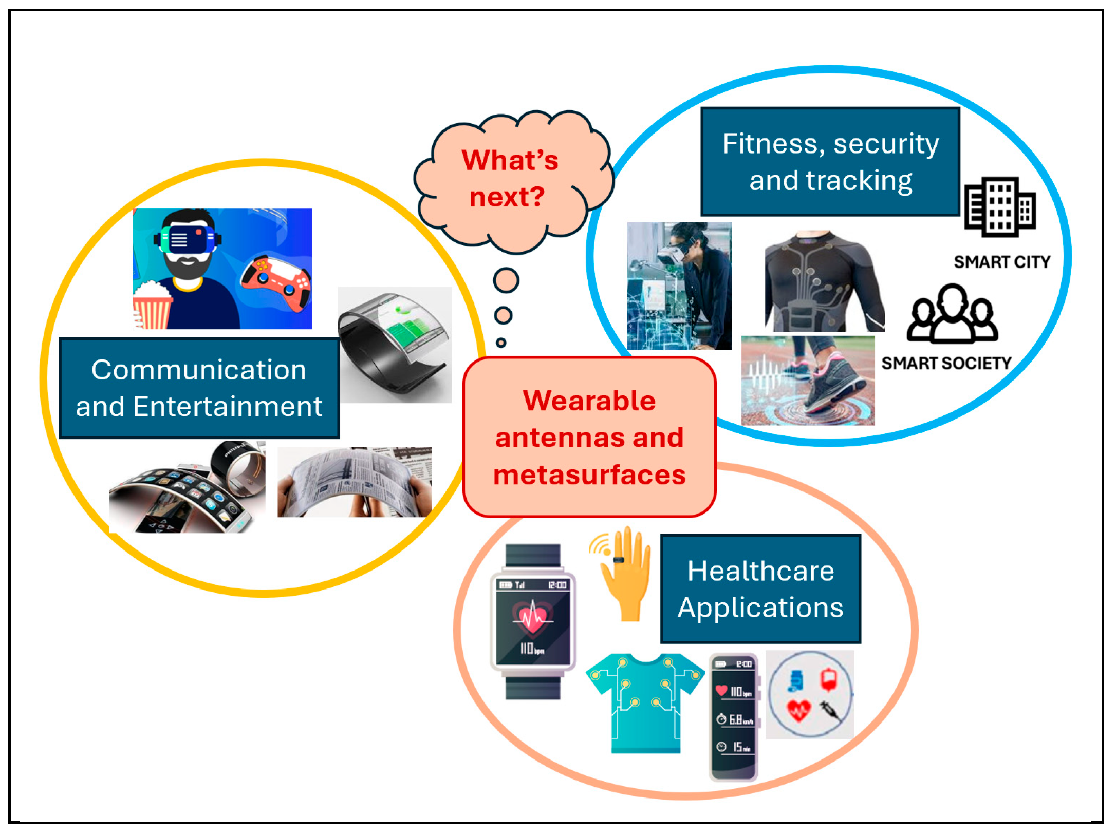
- Current and Future Challenges
Beyond 5G requires moving to the available bandwidth at the mm-wave band to realize applications such as smart cities, the IoE, and virtual reality. This transition towards mm-waves requires antenna designs, indoor base stations, and micro and picocells. Attenuations and atmospheric absorptions at mm-waves are challenging and require proper channel modelling and adopting smart techniques, like massive MIMO, adaptive antennas, and cognitive control systems to improve reliability and system capacity, reduce interference, and obtain high spectral efficiency. Wearable electronics have received massive success in consumer electronics. The fabrication and integration of complex antennas and metasurfaces in wearables is challenging due to several critical requirements. For instance, the design and manufacturing of such new components need a small footprint, high fabrication accuracy, scalability, durability, and cost-effectiveness, and the requirements become more critical for mm-wave antennas having much smaller geometries, and while producing biodegradable antennas using new materials. Current research focuses on developing advanced manufacturing processes and mass-production techniques to make them a practical alternative to traditional antennas.
The performance of wearable antennas may alter significantly due to their environment, such as whether they operate in free space or are worn on-body. For instance, absorption of body moisture, and physical changes in the body due to temperature change, sweating, etc. can impact the antenna performance. The dielectric material used in antenna fabrication is a critical factor as this material should be able to withstand mechanical stresses like bending, crumpling, and stretching. In addition, the conductive part of wearable antennas must be resilient to performance degradations caused by corrosion and mechanical deformations. As the body’s position changes frequently, the movement causes a change in the distance between the transmitter and receiver which eventually causes changes in the free-space path-loss as mm-waves are more affected by absorptions and attenuations than the microwave frequencies. Smaller wavelengths at mm-waves lead to smaller devices and smaller footprints. Precise and high-resolution manufacturing of flexible and conformal mm-wave metasurfaces is significantly challenging due to the smaller geometries of the design.
In addition to antennas, flexible metasurfaces introduce unique challenges. At mm-wave and THz frequencies, the precise fabrication of sub-wavelength unit cells on flexible substrates demands high-resolution and low-cost techniques. Integration with wearable systems requires metasurfaces to be stretchable, breathable, and biocompatible without compromising EM functionality [16]. Furthermore, reconfigurable metasurfaces for wearable or implantable devices must balance tunability, response speed, and power consumption while maintaining safety and reliability [17]. Another emerging challenge lies in the co-design of communication protocols and metasurface control algorithms, which are essential to unlock their potential in practical IoE deployments [18].
- Advances in Science and Technology to Meet Challenges
The research on new conductive textiles, such as conductive polymers, silver/copper-coated fabrics, and graphene layers bonded on polymers has gained massive success in flexible antennas. These materials have good conductivity while stretching, bending and folding, which makes them suitable for wearable devices. Several additive manufacturing techniques have been introduced such as inkjet printing [5], screen printing [6], 3D printing, laser etching [7], etc., however, achieving reasonable accuracy and consistency in bulk manufacturing of much smaller geometries at mm-waves could be a difficult task. Traditional conductive materials are corrosive in moisture and humidity and their use in washable wearables can cause serious concerns to health and the environment. Reported research has indicated the use of carbon-based conductive materials such as graphene and carbon nanotubes which offer high electrical conductivity, good resistance towards corrosion, and high chemical and thermal stability in non-oxidizing environments [8]. Mono-layer graphene and carbon nanotubes offer remarkable electrical properties, and flexibility without significant performance losses, however, industrial-scale graphene manufacturing faces challenges in improving quality control, uniform layer growth, reproducibility of graphene flakes, and increasing mass production and scalability [9].
Further research is needed to understand the characteristics of novel materials and develop methods to mitigate possible hazardous effects and ensure their safe use in communication, healthcare, entertainment, etc. with minimal ecological disruption. In addition, advanced biodegradable materials such as biocompatible conductors, biopolymers, and cellulose-based materials can be used in applications like biosensors, medical implants, and on-body wearable gadgets and costumes, as they are non-toxic to human tissue. This biodegradability makes them suitable for implantable antennas designed for humans and animals in biomedical applications as they can degrade safely in the body after use. Another promising use of biodegradable materials is in sustainable electronics, including antennas for eco-friendly applications to reduce electronic waste (e-waste), especially as more disposable electronics are developed. Graphene and biodegradable materials offer a promising future in mm-wave flexible antennas and printed metasurfaces technology, with each material offering unique advantages for wireless communication beyond 5G and wearables electronics. The high-performance characteristics of graphene at high frequencies, eco-friendliness, and biocompatibility of biodegradable materials, can lead to significant advances in mm-wave antenna designs and metasurfaces. However, challenges related to manufacturing consistencies, performance optimization, and durability require further research and technical efforts before the widespread adoption of these materials.
- Concluding Remarks
In the 5th generation of technology and connectivity, the IoT has emerged as a transformative force, redefining how we interact with the modern world. The deployment of IoT capabilities into wearable devices has enabled seamless communication and created remarkable transformations in wireless security, tracking, healthcare, and entertainment sectors. This article addresses the significant role of mm-wave flexible antennas and metasurfaces in applications beyond 5G/6G, critical challenges, and mitigation measures. For instance, e-textiles are usually designed on similar materials to those used in other commercial electronic devices; metals such as copper, silver and gold, and a range of materials hazardous to the environment. It is essential to explore and implement novel biodegradable materials with properties of washability and susceptibility to corrosion to decrease the global e-waste footprint and keep pace with the recent trend towards flexible implements and wearables. Meeting the requirement for suitable textiles and noncorrosive conductive materials creates new challenges related to miniaturisation, fabrication accuracy, and low-cost manufacturing. Several novel biodegradable materials such as biocompatible conductive inks, biopolymers, and cellulose-based materials can be used in applications like biosensors, medical implants, and on-body wearable uniforms and gadgets due to their non-toxic nature.
A promising future direction lies in developing biodegradable and recyclable metasurfaces based on biopolymers, cellulose nanofibers, and conductive biodegradable inks. Such devices could be designed for short-lifecycle applications (e.g., disposable medical wearables, environmental sensors) where devices naturally degrade after use, thus addressing the growing e-waste crisis. In parallel, hybrid approaches that combine long-lasting graphene-based metasurfaces with biodegradable substrates can strike a balance between performance and sustainability. These proposals pave the way for eco-friendly, high-performance metasurfaces that are compatible with circular economy models in wireless electronics.
- References
- [1]
- G. K. Soni, D. Yadav, A. Kumar and L. Sharma, "Flexible Antenna Design for Wearable IoT Devices," 3rd International Conference on Technological Advancements in Computational Sciences (ICTACS), 2023, pp. 863-867.
- [2]
- M. Jain, D. Kumar, J. Chaudhary, S. Kumar, S. Sharma, and A. S. Verma, “Review on E-waste management and its impact on the environment and society,” Waste Management Bulletin, vol. 1, no. 3, Pages 34-44, 2023.
- [3]
- V. Forti, C. P. Baldé, R. Kuehr, G. Bel, 2020. The global e-waste monitor 2020: quantities, flows, and the circular economy potential.
- [4]
- R. Rajesh, D. Kanakadhurga, and N. Prabaharan, “Electronic waste: A critical assessment on the unimaginable growing pollutant, legislations and environmental impacts,” Environmental Challenges, Vol. 7, 100507, 2022.
- [5]
- S. F. Jilani et al., “Flexible and low-profile inkjet-printed frequency-reconfigurable millimeter-wave MIMO antenna for 5G applications,” Flexible and Printed Electronics-IOPscience, vol. 3, 035003 2018.
- [6]
- S. F. Jilani, O. P. Falade, T. Wildsmith, P. Reip, and A. Alomainy, “A 60-GHz ultra-thin and flexible metasurface for frequency-selective wireless applications,” Applied Sciences, Special Issue: Frequency Selective Surfaces, vol. 9, no.5, 945; 2019.
- [7]
- S. F. Jilani, M. O. Munoz, Q. H. Abbasi, A. Alomainy, “Millimeter-wave liquid crystal polymer based antenna array for conformal 5G applications,” IEEE Antennas and Wireless Propagation letters. vol. 18, no. 1, pp. 84-88, 2019.
- [8]
- D. C.-Amorós, Grand challenges in carbon-based materials research, Speciality Grand Challenge article. Front. Mater., 16 July 2014 Sec. Carbon-Based Materials Volume 1 – 2014.
- [9]
- R. B. Capaz, “Grand challenges in graphene and graphite research,” Speciality Grand Challenge article. Front. Carbon, Sec. Graphite-ene., vol. 1-2022, 2022.
- [10]
- N. Yu and F. Capasso, “Flat optics with designer metasurfaces,” Nature Materials, vol. 13, pp. 139–150, 2014.
- [11]
- S. Abadal et al., “Programmable metamaterials for software-defined electromagnetic control: Circuits, systems, and architectures,” IEEE J. Emerging Sel. Topics Circuits Syst., vol. 10, no. 1, pp. 6–19, 2020.
- [12]
- M. Di Renzo et al., “Smart radio environments empowered by reconfigurable intelligent surfaces: How it works, state of research, and the road ahead,” IEEE J. Sel. Areas Commun., vol. 38, no. 11, pp. 2450–2525, 2020.
- [13]
- C. Liaskos et al., “A new wireless communication paradigm through software-controlled metasurfaces,” IEEE Commun. Mag., vol. 56, no. 9, pp. 162–169, 2018.
- [14]
- Q. Wu and R. Zhang, “Towards smart and reconfigurable environment: Intelligent reflecting surface aided wireless network,” IEEE Commun. Mag., vol. 58, no. 1, pp. 106–112, 2020.
- [15]
- A. Alomainy et al., “Wearable and flexible body-centric antennas for wireless communications and bio-sensing: A review,” IEEE Trans. Antennas Propag., vol. 66, no. 4, pp. 2184–2197, 2018.
- [16]
- J. Shabanpour et al., “Stretchable and conformal metasurfaces: Materials, fabrication, and applications,” Advanced Functional Materials, vol. 32, 2022.
- [17]
- Z. Zhang et al., “Reconfigurable intelligent surfaces for 6G: Design, challenges, and opportunities,” IEEE Internet Things J., vol. 8, no. 13, pp. 10452–10467, 2021.
- [18]
- E. Basar et al., “Reconfigurable intelligent surfaces for wireless communications: A vision, opportunities, and challenges,” Proc. IEEE, vol. 108, no. 9, pp. 1536–1564, 2020.
9. Superscatterers
Alex Powell1, Stephen Henthorn2
1Centre for Metamaterial Research and Innovation, University of Exeter (a.w.powell@exeter.ac.uk)
2School of Electrical and Electronic Engineering, University of Sheffield (s.henthorn@sheffield.ac.uk)
- Status
The ability to enhance electromagnetic scattering from small, subwavelength structures is of great significance across fields as diverse as antenna design, RFID, backscatter communications and remote sensing. For any given electromagnetically resonant structure, there is a theoretical limit to how much a single scattering channel can interact with incident radiation – this is referred to as the ‘single channel limit’. The maximum scattering cross section (SCS) defined by the single channel limit can be written for 2D and 3D structures[1,2] as-
where n is the surrounding refractive index.
Superscattering structures are designed in such a way that they can significantly beat this limit. This is generally achieved by creating a system where multiple resonances occur at a given frequency (‘mode stacking’ – Figure 1a)), although recently other methods have been demonstrated. Mode-stacking is typically achieved by controlling the internal structure of a scatterer, either to create multiple layers with different resonances that can be designed to occur at the same frequency[3,4], or by selectively altering certain resonances of an existing structure so they occur at the same frequency as others[5–7].
The mode stacking approach provides additional advantages over conventional scatterers, as it enables the tuning of the bandwidth, directionality, phase and magnitude of the scattering cross section through controlling interference of radiation scattered by different resonant modes. This can be utilised to produce either omnidirectional or highly directive scattering (despite the compact size of the scatterers), or to completely suppress the backscatter or forward scatter of the system at a given frequency[8]. The early theory of superscattering was laid out by Ruan & Fan in 2010[3], and over the past decade or so there has been significant interest in creating structures that generate this effect.
Applications for microwave superscatterers range from antenna design[9,10] (both driven antennas and backscatter comms), to energy harvesting[11], to the radar detection of small objects like quadcopter drones.
Figure 1.
a) An illustration of the principle of superscattering via ‘mode stacking’ [4]. b) A multilayer metamaterial superscattering cylinder that can stack three resonant scattering channels[4]. c) A 3D printed localised spoof plasmon superscatterer[12]. d) A wire bundle superscatterer[13]. e) A gain metasurface superscatterer[14].
- Current and Future Challenges
Whilst there have been many demonstrations of superscatterers in the literature, few of these have materialised into workable applications. The challenges in the field of superscatterers can be largely broken down into three categories: directivity, bandwidth, and fabrication.
In terms of directivity, whilst three or more modes have been successfully superimposed to give powerful superscattering an order of magnitude above the single channel limit, a problem faced by this approach is that when many modes are superimposed, unless great care is taken, the interference in the far field will suppress backscatter and enhance forward scattering[6,7]. So whilst the SCS value can seem impressive, the (generally useful more useful) backscattering can actually be supressed compared to that of a simple, single resonance scatterer.
Another key challenge with superscatterers is the highly narrow bandwidths of operation necessitated though the operation of scattering by several modes at once. Due to the necessary involvement of higher order, high-Q modes, these structures tend to be highly narrowband. Research to improve the bandwidth and/or produce reconfigurable superscatterers, would strongly enhance their utility for many applications.
In terms of fabrication, many superscatterers require either complex layers of metamaterials and dielectrics, or expensive, heavy ceramics to operate, which reduces their utility in many applications. Moving to more compact, lighter weight materials will be key for moving from scientific demonstrators towards applications.
- Advances in Science and Technology to Meet Challenges
Recently there has been increasing diversification in the type of superscatterers available. Ginzburg et al have designed superscatterers based on wire bundle structures (Figure 1d)[13], which are very compact, easy to fabricate, and lightweight but with a strong scattering response. A disadvantage of these designs is that they are strongly forward scattering, and it has yet to be demonstrated if they could be optimised for improving backscatter. 3D printed structures(Figure 1c) have also taken a foreground, which are simple and relatively cheap to fabricate, and can be designed to be broadband[12,16], but at a reduced scattering power.
Another design that takes a different approach, has been shown by Qian et al[14], who created a single channel superscatterer using a circular metasurface with gain components (Figure 1e). This means that a single resonant channel can scatter radiation far in excess of the theoretical limit, and as there is no interference between modes, so a strong degree of backscatter can also be achieved. The disadvantage here is that this material is not totally passive and does require a modest power source.
Whilst recent advances have approached some of the challenges faced by superscatterers, there remain significant issues to be addressed. To the author’s knowledge there has been no attempt so far to make tunable electromagnetic superscatterers at RF frequencies, although interestingly, this has recently been demonstrated for acoustics[17]. This is surprising, as the potential for active superscatterers seems obvious, e.g. for compact IoT/backscatter communications tags, or environmental sensors. As there can be three or more resonances in a very small frequency space, significant control over the phase, and scattering power, (both as a function of direction) can be achieved by switching different resonances on or off. This enables a wide range of waveforms to be modulated onto scattered signals. Wire-based tunable superscatterers could be made reconfigurable using similar techniques to tunable metamaterials, such as integrating varactor diodes or other electronic components, though control of the separate modes presents interesting research challenges [18]. Meanwhile dielectric superscatterers may be produced using phase change media or fluidics.
- Concluding Remarks
Superscatterers have demonstrated an unprecedented level of control over the manner in which a subwavelength structure can interact with, and redirect electromagnetic radiation. Previous works show that through utilising ‘mode stacking’, (as well as other approaches), significant control over the power, directivity and bandwidth of the scattering cross section of small objects can be achieved. However, challenges remain in terms of maximising backscatter, fabrication and bandwidth. For future work we recommend firstly more research into gain-based superscatterers, possibly combining the properties of these scatterers with a mode stacking approach. And Secondly, the design and creation of ‘active superscatterers’, where resonances can be switched on or off to modulate the phase, power, and directivity of scattering, and whose greatly increased versatility will enable applications in backscatter communications, antennas, RFID and environmental sensing.
- References
- [1]
- J. Aizpurua, P. Hanarp, D. S. Sutherland, M. Käll, G. W. Bryant, and F. J. García de Abajo, “Optical Properties of Gold Nanorings,” Phys. Rev. Lett., vol. 90, no. 5, p. 4, Feb. 2003.
- [2]
- M. I. Tribelsky and B. S. Luk’yanchuk, “Anomalous light scattering by small particles,” Phys. Rev. Lett., vol. 97, no. 26, p. 263902, Dec. 2006.
- [3]
- Z. Ruan and S. Fan, “Superscattering of light from subwavelength nanostructures,” Phys. Rev. Lett., vol. 105, no. 1, p. 013901, Jun. 2010.
- [4]
- C. Qian et al., “Experimental Observation of Superscattering,” Phys. Rev. Lett., vol. 122, no. 6, p. 063901, Feb. 2019.
- [5]
- W. Liu, J. Zhang, B. Lei, H. Ma, W. Xie, and H. Hu, “Ultra-directional forward scattering by individual core-shell nanoparticles,” Opt. Express, vol. 22, no. 13, p. 16178, Jun. 2014.
- [6]
- I. Liberal, I. Ederra, R. Gonzalo, and R. W. Ziolkowski, “Superbackscattering from single dielectric particles,” J. Opt. (United Kingdom), vol. 17, no. 7, p. 072001, Jul. 2015.
- [7]
- A. W. Powell, A. P. Hibbins, and J. R. Sambles, “Multiband superbackscattering via mode superposition in a single dielectric particle,” Appl. Phys. Lett., vol. 118, no. 25, p. 251107, Jun. 2021.
- [8]
- M. Kerker, D. S. Wang, and C. L. Giles, “Electromagnetic scattering by magnetic spheres,” JOSA, Vol. 73, Issue 6, pp. 765-767, vol. 73, no. 6, pp. 765–767, Jun. 1983.
- [9]
- A. E. Krasnok, D. S. Filonov, C. R. Simovski, Y. S. Kivshar, and P. A. Belov, “Experimental demonstration of superdirective spherical dielectric antenna,” Appl. Phys. Lett., vol. 104, no. 13, Nov. 2022.
- [10]
- A. W. Powell, M. Mrnka, A. P. Hibbins, and J. Roy Sambles, “Superscattering and Directive Antennas via Mode Superposition in Subwavelength Core-Shell Meta-Atoms,” Photonics 2022, Vol. 9, Page 6, vol. 9, no. 1, p. 6, Dec. 2021.
- [11]
- Z. Qin et al., “Superscattering of water waves,” Natl. Sci. Rev., vol. 10, no. 7, May 2023.
- [12]
- A. W. Powell, T. E. Whittaker, W. G. Whittow, J. R. Sambles, and A. P. Hibbins, “Demonstration and Control of ‘Spoof-Plasmon’ Scattering from 3D Spherical Metaparticles,” ACS Photonics, vol. 17, p. 49, Mar. 2023.
- [13]
- S. Kosulnikov et al., “Circular wire-bundle superscatterer,” J. Quant. Spectrosc. Radiat. Transf., vol. 279, p. 108065, Mar. 2022.
- [14]
- C. Qian et al., “Breaking the fundamental scattering limit with gain metasurfaces,” Nat. Commun. 2022 131, vol. 13, no. 1, pp. 1–7, Jul. 2022.
- [15]
- D. Dobrykh et al., “Multipole engineering for enhanced backscattering modulation,” Phys. Rev. B, vol. 102, no. 19, p. 195129, Nov. 2020.
- [16]
- A. Mikhailovskaya et al., “All-angle All Polarization Broadband ‘Corona’ Scatterer,” 2022.
- [17]
- V. P. Ramachandran and P. Rajagopal, “Tunable acoustic superscatterer composed of magnetorheological fluid and maze-like metasurface,” J. Sound Vib., vol. 574, p. 118184, Mar. 2024.
- [18]
- G. Oliveri, D. H. Werner and A. Massa, "Reconfigurable Electromagnetics Through Metamaterials—A Review," Proc. of the IEEE, vol. 103, no. 7, pp. 1034-1056, Jul. 2015.
10. Conclusions and Future Directions
Akram Alomainy1, Qammer H Abbasi2 and Stephen D Henthorn3
1School of Electronic Engineering and Computer Science, Queen Mary University of London (a.alomainy@qmul.ac.uk)
2James Watt School of Engineering, University of Glasgow (Qammer.Abbasi@glasgow.ac.uk)
3School of Electrical and Electronic Engineering, University of Sheffield (s.henthorn@sheffield.ac.uk)
The Roadmap presents a comprehensive overview of the current state, challenges, and emerging opportunities for metamaterials across wireless communications, sensing, healthcare, defence, and manufacturing. The field of microwave and wireless metamaterials is undergoing a transition, from foundational scientific exploration to system-level deployment, driven by innovations in materials, design, computation, and integration.
- Conclusions
- Fundamental Research
The evolution of metamaterials has moved beyond conceptual explorations to focus on enhanced control of electromagnetic waves through structured materials. Fundamental research has enabled key functionalities, such as programmable phase control, beam shaping, polarisation manipulation, and spectral selectivity. Particularly notable is the development of Reconfigurable Intelligent Surfaces (RIS), which embody the convergence of electromagnetics, control theory, and communications engineering. THz metasurfaces are also emerging as critical tools for future 6G networks, enabling joint communication and sensing capabilities with unprecedented resolution.
Nonetheless, the field faces significant scientific challenges. Resonance-based behaviour, angular dependence, and narrow operational bandwidths remain limiting factors. Additionally, simulation and modelling tools must evolve to incorporate fabrication tolerances, environmental variability, and multiphysics interactions across electrical, thermal, and mechanical domains.
- Applied Research
From an applied perspective, metasurfaces are poised to transform wireless networks, healthcare monitoring systems, radar and stealth technologies, and bioelectronic implants. In 5G and beyond, metasurfaces offer a paradigm shift—turning passive environments into programmable communication media. RIS-enabled systems are beginning to demonstrate tangible gains in signal strength, energy efficiency, and spatial coverage. In healthcare, RIS and metasurfaces are powering non-invasive sensing, localisation, and wireless power transfer to wearable and implantable devices.
Moreover, radar cross section (RCS) reduction using metasurfaces is progressing toward adaptive, lightweight, and conformal designs for stealth applications. Flexible, scalable, and low-loss metasurfaces are now being actively researched for deployment on curved and complex platforms. However, a key limitation in all these sectors remains the difficulty of translating lab-scale prototypes into robust, mass-producible solutions.
- Future Directions
The roadmap identifies several strategic directions to advance the field of wireless and microwave metamaterials, across both fundamental and applied dimensions:
- A.
- Intelligent and Adaptive Metasurfaces
Future metasurfaces will need to be self-configuring, context-aware, and autonomously adaptive. This calls for tighter integration of AI/ML algorithms to optimise design, manage tuning states in real-time, and adapt to dynamic electromagnetic environments. Intelligent surfaces will not only reflect or transmit waves but will become functional nodes within cyber-physical systems.
- B. New Material Platforms
Breakthroughs in material science are central to the next wave of innovation. Research into flexible, stretchable, biocompatible, low-loss, and transparent materials will enable novel applications, from wearable electronics to space-conformal radar coatings. In parallel, nonlinear and quantum metasurfaces could unlock advanced functionalities for sensing, imaging, and secure communication.
- C. Scalable and Sustainable Manufacturing
As the field matures, design-for-manufacture principles must be embedded into early-stage research. Techniques such as additive manufacturing, roll-to-roll processing, and hybrid fabrication offer viable paths forward but require further alignment with electromagnetic performance requirements. Sustainability considerations—such as recyclability, energy use in production, and end-of-life strategies—must become embedded in design cycles.
- D. Multiphysics and Multiscale Modelling
To bridge the gap between design and deployment, new computational frameworks are needed. These must simultaneously model electromagnetic, mechanical, and thermal behaviours across multiple length scales, from subwavelength meta-atoms to system-level enclosures. Such models will support the co-design of metasurfaces with antennas, packaging, electronics, and controllers.
- E. Energy Efficiency and Harvesting
Powering metasurfaces remains a challenge, particularly for remote and embedded applications. Research into ultra-low-power control circuits, energy harvesting, and wireless powering architectures will be essential. In healthcare, for example, wireless metasurfaces must operate safely within human tissue while maintaining stable performance over time.
- F. Integration with Communication and Sensing Systems
Future networks—whether in 6G, vehicular autonomy, or smart infrastructure—will require metasurfaces to function as system components, not standalone elements. This involves integration with RF front-ends, digital control, localisation algorithms, and even cryptographic systems for security. Joint communication and sensing platforms will increasingly rely on metasurfaces for spatial and spectral agility.
- G. Ethical, Legal, and Regulatory Alignment
Widespread deployment of metasurfaces in public and personal domains introduces new regulatory and ethical considerations. Issues such as electromagnetic exposure limits, data privacy in sensing applications, and shared-spectrum coexistence require urgent attention. Engaging with policymakers and standardisation bodies (e.g., ETSI, ITU) will ensure responsible innovation.
- H. Interdisciplinary and Cross-Sector Collaboration
The future of metamaterials is interdisciplinary. Achieving their full potential requires collaboration among materials scientists, electromagnetics engineers, communication theorists, data scientists, and system integrators. Furthermore, partnerships with industry and government agencies will accelerate technology translation and policy alignment.
- The Road Ahead
Microwave and wireless metasurfaces are reaching an inflection point. Their promise extends far beyond niche applications, touching nearly every sector reliant on electromagnetic systems. However, realising their full impact demands a shift from component-centric thinking to system-level, application-driven design. The research community is now challenged to innovate not just in discovery, but in translation, scalability, and societal integration.
As this roadmap illustrates, the UK metamaterials community is well-positioned to lead in this field. Continued investment in fundamental science, practical engineering, manufacturing readiness, and cross-sector collaboration will ensure metamaterials become a core pillar of next-generation wireless and microwave technologies.
Disclaimer/Publisher’s Note: The statements, opinions and data contained in all publications are solely those of the individual author(s) and contributor(s) and not of MDPI and/or the editor(s). MDPI and/or the editor(s) disclaim responsibility for any injury to people or property resulting from any ideas, methods, instructions or products referred to in the content. |
© 2025 by the authors. Licensee MDPI, Basel, Switzerland. This article is an open access article distributed under the terms and conditions of the Creative Commons Attribution (CC BY) license (https://creativecommons.org/licenses/by/4.0/).
Copyright: This open access article is published under a Creative Commons CC BY 4.0 license, which permit the free download, distribution, and reuse, provided that the author and preprint are cited in any reuse.


