Submitted:
23 September 2025
Posted:
23 September 2025
You are already at the latest version
Abstract
This paper deals with diamond films grown by microwave plasma enhanced chemical vapor deposition technique (MWPECVD) on molybdenum (Mo) substrates of different roughness. The work is motivated by the necessity to overcome the poor adhesion of diamond films on smooth Mo substrates, to be effectively applied as cathodes for aerospace propulsion. The deposition process was monitored in situ by pyrometric interferometry (PI), thus enabling the real-time monitoring of both the rate and the temperature of deposition. The characterization of the obtained diamond films was performed by different techniques such as Raman spectroscopy, X-ray diffraction (XRD) and scanning electron microscopy (SEM). The poor adhesion of diamond films on smooth Mo was solved by roughening the surface substrates, decreasing thermal and intrinsic stresses of the films compared to those depos-ited on smooth ones. In this work, PI technique supported the prediction of the adhesion and the stability of diamond films before their exposure in air, simply by monitoring the deposition temperature. This is a very interesting aspect that has never been addressed in research papers, as pyrometric interferometry is generally used to assess the rate and the temperature of deposition.
Keywords:
MWPECVD
; diamond films
; molybdenum substrate
; surface roughness
1. Introduction
The superior chemical-physical properties of diamond, such as high chemical inertness, high mechanical hardness, high radiation hardness, good thermal conductivity and high secondary electron emission coefficient, make it one of the most investigated in the field of materials research. In particular, the chemical inertness allows it to work under harsh external conditions. Diamond is also a wide band gap semiconductor (5.47 eV) thus implemented in UV sensors [1,2]. In addition, it is a good electron emitter for its low electron affinity (0.35 - 0.5 eV), making it attractive for photocathode production, especially in nanocrystalline structure [3,4,5,6,7,8].
Since the synthesis of diamond films was generally carried out by chemical vapor deposition (CVD) techniques, such as hot filament CVD (HFCVD) [9] and microwave plasma enhanced CVD (MWPECVD) [2,4,5,6,10], working at high deposition temperatures (≥600 °C), the employed substrates must be compatible with the growth process of diamond. The role of the substrate in diamond films growth was crucial, because it affected many diamond properties, like the structure, the microstructure, the morphology, and the adhesion. This was the reason why the choice of substrate for diamond deposition must have certain requirements [11]. First, it must be resistant to high temperature and have thermal expansion coefficients or lattice constants close to those of diamond. Second, it must be able to form carbides as intermediate layer having high surface free-energies relatively close to the surface free energy of diamond [12,13,14,15,16]. Refractory metals (Mo, W, Ta), as well as silicon, form stable carbides in the presence of carbon or hydrocarbons due to their high stability and to the low carbon solubility in these metals. For example, W forms W2C at 920-970 °C, Mo forms Mo2C at 700-770 °C [12] and SiC is the predominant form of the intermediate layer when using silicon as substrate. The carbon surface diffusion on the substrate is mainly important for the diamond nucleation [11]. For example, Ta and W have shown very low carbon diffusion into the substrate making the diamond growth [11] difficult; high nucleation rates are instead observed with Nb and Mo substrate [11]. In addition, the carbon diffusion coefficient together with the substrate temperature and the carbon concentration influence the carbide layer growth rate that is relatively slow, providing very thin layer thickness of the order of 1–10 nm, as reported by some authors for SiC intermediate layer when diamond is deposited on silicon substrate using MWPECVD technique [13,14,15]. Carbide layers play an important role for the mechanical [16] and the structural properties of the grown diamond film (sp2/sp3 carbon content, grain size, orientation of growth), thus modifying microhardness and corrosion resistance of the material [12].
Most papers reported in literature show diamond synthesized on molybdenum [9,17,18,19,20,21], conventional silicon substrates [17,21,22] and copper [17,18,19,20,21], mainly thanks to their high melting point temperature, making them utilizable in CVD techniques. Moreover, the lattice constants close to that of diamond make them good for heteroepitaxy deposition, especially Cu and Mo. Among conductors, molybdenum is considered the best substrate for diamond growth [11,17,18,19], thanks to the lattice constant and thermal expansion close to diamond. It is also a refractory metal with a high melting point (2623 °C) and therefore extraordinarily resistant to high temperatures. However, silicon is generally the most utilized substrate material for diamond growth by CVD techniques having a thermal expansion coefficient very close to that of diamond although its small nucleation density of 104 cm-2, due to the high surface diffusivity of the carbon species.
Table 1 summarizes the above-discussed key properties of the main substrates suitable for diamond thin films growth and compares them with diamond ones.
In general, the high surface energy of diamond makes it extremely difficult to grow on non-diamond substrates [23]. Therefore, such a problem has been solved by using techniques that promote the nucleation process and enhance the density of the nuclei up to 1010 cm-2 on silicon substrate [24]. One approach is the pre-treatment of the substrates [11,22,24,25,26], consisting in ultrasonic abrasion, using diamond particles ranging from 10 nm to 45 m. Another way to treat the substrate surface, but less widely used, is mechanical scratching with diamond powder [20], to induce morphology modifications able to create active sites for a better adsorption of diamond precursors. This step is extremely important in the first phase of the growth: a mirror or flat surface does not promote diamond nucleation, since there are neither (a) appropriately shaped scratches in the surface, which act as growth templates, or (b) embedding nanometre-sized fragments of diamond into the surface, which then act as seed crystals, or (c) a combination of both.
On metal substrates CVD-grown diamond films exhibit good adhesion [11,21], although some authors report their detachment [27]. In particular, diamond films on Mo substrates exhibit enhanced adhesion on roughened surfaces [21].
The aim of this work is to study the impact of the Mo substrate roughness on the properties of the diamond films to overcome the poor adhesion and stability of the films on smooth Mo substrate observed in samples to be tested as neutralizer cathode for aerospace applications. The films were grown by MWPECVD technique and both the rate and the temperature of deposition during the process were monitored in situ by pyrometric interferometry (PI).
In this work, we also demonstrate how the deposition temperature can be considered a key parameter for the production of adherent and high-quality diamond films. The characterization of the diamond films was performed by means of atomic force microscopy (AFM) to evaluate the substrate roughness, by X-ray diffraction (XRD) to evaluate the crystallinity, the average orientation, the size of the crystalline grains and the residual stress; Raman spectroscopy to assess the carbon hybridization and the phase purity, and scanning electron microscopy (SEM) to determine the films’ surface morphology.
Finally, we show initial tests on cathode erosion in Ar plasma in order to obtain a preliminary estimate of the stability of these films as cathode in a plasma environment, as occurs when they are applied in aerospace propulsion.
2. Materials and Methods
Diamond films were deposited on molybdenum and silicon substrates by MWPECVD technique in a home-made cylindrical stainless steel ASTeX-type reactor, by starting from CH4-H2 gas mixture.
2.1. Substrates Preparation
Four types of substrates were used in this study: a disk of p-Si (highly doped in boron with a low resistivity <0.005 ohm·cm, single side polished, diameter of 25 mm and thickness of 0.75 mm) and three disks of smooth Mo (diameter of 25 mm, thickness of 0.75 mm). One Mo disk was used as received (MoS) while the other two were mechanically treated, by two different methods, to roughen the surface and study the influence of the surface roughness on the adhesion of diamond film on it.
The first available method was sandpaper. The sanding operation was performed manually by P60 sandpaper with grit particles size of 269 m (MoRsandpaper) to achieve a coarser surface. This treatment was performed for 10 minutes applying a constant force of about 10 N/cm2. Subsequently, the opportunity to use a shot peening machine CB800PA series A was seized, improving the quality of the roughness treatment (uniformity and better control of surface modification). A jet of alumina powder was used on the Mo sample (MoRshot-peened) placed at a distance of 10 cm for a duration of 15 minutes. After these treatments, the Mo substrates were cleaned with alcohol and deionized water to remove any residual dirt and debris. The root mean square roughness (Rq) of the substrates was evaluated by AFM (Nanosurf CoreAFM).
2.2. Diamond Deposition via MWPECVD Technique
Before the introduction into the deposition chamber of MWPECVD apparatus, the p-Si and Mo substrates were treated ultrasonically for one hour in an ethanol suspension of diamond powder (grain size 40-60 µm). Such treatment enhanced the nucleation density [24] by promoting the deposition process of diamond films. During the plasma-chemical process the substrates were directly placed on the susceptor, previously heated up to 700 °C via a PID (Proportional Integral Derivative) feedback control system. A highly diluted mixture of CH4:H2 was employed 2.5:247.5 sccm (standard cubic centimeters per minute), the total gas flow rate was 250 sccm. The flow rate of each gas was controlled via a flowmeter and kept constant during the whole process. The deposition time was monitored to obtain films of thickness around 1 µm.
In the following Table 2, the deposition parameters for the preparation of the samples are listed, holding constant composition of gas mixture (1% CH4 - 99%H2), total gas flow rate (250 sccm), susceptor height (70 mm), microwave power (1250 Watt) and pressure (35 mbar).
2.3. Process Diagnostics: Pyrometric Interferometry (PI)
As already reported, the on-line, real-time and continuous measurement of the surface temperature of the substrate on which the diamond deposition takes place is very important. It allows for measuring the deposition rate and thus the average thickness of the obtained film, and it is also shown how a check can be obtained on the adhesion properties of the film by observing the pyrometric interferogram and the deposition temperature during the diamond growth process.
In the experiment, the temperature was measured by the pyrometric interferometry that is a non-invasive, in-situ diagnostic technique of the plasma chemical process which allows the monitoring of temperature in real time. Specifically, a noncontact, dual wavelength infrared (1 = 2.1 m and 2 = 2.4 m) pyrometer (Williamson Pro 9240) working in the temperature range 475-1475 °C was employed. It was positioned on the upper quartz window of the MWPECVD reactor by means of the optical fiber, set perpendicular to the substrate surface with an observation angle = 0°, and interfaced to the computer by means of a programmable interface module. The emitted IR radiation intensity is modulated in time by interference phenomena causing a variation of the apparent temperature reading of the pyrometer. The real deposition temperature (TD) of the process can be calculated through the average value. In addition, the pyrometric interferences provide also the deposition rate rD according to the following equation [28]:
where 1 and 2 are the two wavelengths of the pyrometer, is the observation angle measured from the substrate surface normal, n is the refraction index of the diamond film (about 2.4), and t is the time interval between two consecutive maxima or minima of the apparent temperature oscillations).
The used pyrometer offers the following advantages:
- the two wavelengths allow to compensate automatically the problems due to emissivity variation;
- the chosen wavelengths allow to observe the specimen surface through the plasma without contributions from the latter;
- the long-term stability of the calibration is useful for monitoring processes or controlling applications where precise and reproducible results can be a crucial point;
- the values of the quality factor known as Signal Dilution Factor (500:1) are high;
- the optical fiber permits to place the sensor in more convenient and remote zones.
2.4. Diamond Films Characterization
The material characterization plays an important role both for the optimization of the plasma chemical process and for the behavior of the film diamond in the application of final device.
The topography of the p-Si and molybdenum substrates was analyzed by AFM technique (Nanosurf CoreAFM) operating in contact mode in air at room temperature by scanning an area of (10 x 10) m2.
The topography and morphology of the diamond surfaces were investigated by SEM. The SEM images were obtained using an EVO scanning electron microscope (SEM model Zeiss 50XVP) in secondary electrons mode, with an operating voltage of 15 kV. This technique allows to obtain magnification up to 106, therefore the morphology of various materials can be analyzed with a spatial high resolution down to few nm.
The chemical-structural features of diamond films were examined at room temperature by means of a Raman confocal micro-spectrometry apparatus (Labram from Jobin-Yvon Horiba) in the backscattering configuration using an excitation Ar-ion laser beam (514 nm, laser output power 1 mW). The spot size on the samples was approximately 1 µm diameter using a 100x objective. Raman spectroscopy permits the evaluation of order and structure of the various carbon allotropes via the analysis of the position and the shape of the phonon peaks, allowing to distinguish sp2 (graphite) and sp3 (diamond) hybridized carbon.
The crystalline structure and the crystal orientation of the diamond films were analyzed by XRD technique (Rigaku SmartLab SE diffractometer, Tokyo, Japan) in pseudo-parallel Bragg–Brentano mode with an incident angle of 0.5°, using the Cu-Kα radiation (λ=0.154 nm, 40 kV and 50 mA) and the spectra were collected in 2θ = 10°– 80° (0.010° step size and scan speed of 0.2° min-1). The spectra were fitted by a Voigt function to calculate the full width at half maximum (FWHM) for crystal quality assessment. The crystallite size of the thin films was extracted from the XRD data.
3. Results and Discussion
Figure 1 shows: a) the photos of molybdenum substrates, b) the corresponding AFM topography images, with and without roughening treatments and c) AFM profiles.
The topography of the polished p-Si substrate, studied using AFM, showed an average roughness of less than 1 nm (not shown in Fig. 1). The smooth Mo surface (MoS), on the other hand, had a higher roughness of (70 ± 5) nm, which was very different from that of the polished p-Si, which increased to (580 ± 50) nm when roughened by shot peening (MoRshot-peened) and up to (675 ± 65) nm when treated by sandpaper (MoRsandpaper). Furthermore, it can be seen from the AFM images of Fig.1b that the roughness of the shot peened molybdenum is regular and uniform over the entire surface (due to the uniform shot of particles), in contrast to the sandpaper roughened molybdenum, which shows grooves in different directions with depths around 1 m (see Fig. 1c), compatible with the specifications of the sandpaper used.
Figure 2 shows the Mo roughness with and without the application of the roughening treatments. In the same Figure, the Si roughness is reported for comparison.
Figure 3 shows the pyrometric interferograms obtained during the deposition process of Diam112 on polished p-doped silicon (Diam112_pSi, blue curve) and Diam116 on smooth Mo (Diam116_MoS, red curve), without the roughening treatment.
The deposited film thicknesses (reported in Table 2) are calculated by multiplying the rD of eq. (1) and the deposition time.
Although both samples were synthesized under the same experimental conditions, it is worth to evidence that the apparent temperature recorded on each substrate is very different. In particular, minima and maxima of the interference fringes of Diam116_MoS, are below and above the sensor’s range of measurements and are recorded as LO (below range i.e. < 475 °C) or HI (above range i.e. > 1475 °C). The value of real deposition temperature (TD), given by the averaged values of apparent temperatures, is indicated in Figure 3 by the horizontal blue line for Diam112_pSi (TD = 820 °C), while it was not possible to calculate it for Diam116_MoS (interpolation gives TD > 950 °C).
The results change when comparing the temperatures obtained during the synthesis of the diamond films on rough Mo substrates. Figure 4 reports, in fact, the pyrometric interferograms of Diam116_MoS (red curve) and Diam117 grown on roughened Mo by sandpaper (Diam117_MoRsandpaper, blu curve) which shows a clear decrease of deposition temperature from TD > 950 °C to 873 °C. The roughening treatment of Mo induces a pyrometric interferogram where the maxima and minima values of interference fringes are within the measurement range of the pyrometer (475 °C < T < 1475 °C) and therefore a lower deposition temperature.
The subsequent opportunity to improve roughness treatment through shot peening made it possible to decrease the temperature of the process. In fact, a lower deposition temperature was observed for Diam114_MoRshot-peened. The pyrometric interferogram reported in Figure 5 falls even better within the operating range of the pyrometer with an estimated deposition temperature of 818 °C (Diam114_MoRshot-peened, blue curve).
After deposition and successive susceptor cooling, all diamond films were removed by the deposition chamber and exposed to air atmosphere and characterized by AFM, XRD, Raman and SEM techniques.
Figure 6 shows the XRD patterns of the diamond films, performed in -2 (Bragg-Brentano) geometry, from 0 to 80 degree. The labels showed, for all the investigated films, the diffraction peaks corresponding to two orientation planes of cubic diamond. Specifically, the peak at 2 = 43.9° belongs to the diffraction from the crystallographic plane (111) of diamond; the other peak at 2 = 75.3° is attributable to the diffraction from (220) plane of cubic diamond.
All the spectra of the diamond films also show the reflection from their substrates. In particular, Diam112_pSi pattern shows two peaks at 2 = 32.9° and 69.1°, corresponding to the (200) and (400) crystalline planes of silicon, respectively. The spectra of Mo substrate, Diam116_MoS, Diam114_MoRshot-peened and Diam117_MoRsandpaper show three peaks located at 40.6°, 58.8° and 73.8°, corresponding to the (110), (200) and (211) crystalline planes of molybdenum (JPCDS 89-5023), respectively. A low intensity peak due to molybdenum oxide (MoO2) is also visible in the Mo substrate spectrum.
In addition to the reflection peaks of diamond films and the corresponding substrates, all the spectra show various peaks attributable to metal carbide interlayer. In particular, the spectrum of Diam112_pSi shows a very high and narrow peak of 3C-SiC whereas Diam116_MoS, Diam114_MoRshot-peened and Diam117_MoRsandpaper show various strong reflection peaks attributed to -Mo2C (exagonal carbide phase, JCPDS 35-0787).
X-rays reflections provide information also about the interfaces suggesting that, before the growth of diamond films, very thin layers of Mo2C and SiC were produced on the substrates surface; consequently, diamond films grow on the respective carbide layers. The roughening of the Mo substrates does not influence the crystallinity of the diamond films showing the same diffractograms, whatever the substrate surface conditions are. On the contrary, a strong influence on the microstructure can be observed through the estimation of the crystallite size of diamond films. Grains size (Gs) along (111) and (220) planes of diamond were calculated by Scherrer formula [29] and by fitting XRD peak with a Voigt function. The obtained values are reported in Table 3.
It is worth to note that all the diamond films grow preferentially along (111) plane, as confirmed by the faster growth of (111) grain size. In addition, the grain size decreases with substrate roughness increasing, as depicted in Figure 7.
The lattice constant was also calculated, considering Bragg Law. The lattice constant of stress-free diamond (cubic carbon) is 0.357 nm which is 34 % smaller than that of Si (0.543 nm) and 12 % larger than that of Mo (0.314 nm). Considering the XRD spectra of Figure 6, an interlayer of carbide appears on all the substrates. The lattice parameters for -Mo2C are a = 0.30 nm and c = 0.473 nm (JCPDS no. 11–0680). SiC has more than 250 different polytypes but usually exists in two basic crystalline modifications - hexagonal -SiC (6H-SiC (a = 0.3073 nm, с = 1.511 nm) and cubic -SiC (3C-SiC a = 0.43596 nm). Lattice mismatches between diamond and molybdenum/silicon carbides are 19 % (larger) and 22 % (smaller), respectively.
The dislocation density (δ) gives more information about the number of defects in the films which can be calculated from Williamson-Smallman relation [30]:
where the grain size GS is expressed in nm. Higher δ values indicate lower crystallinity levels for the films and the number of defects in the structure. All diamond films arrange along (111) plane with higher crystallinity. The number of crystallites per unit area (N) can be calculated from the following formula:
where t is the thickness of the film. The higher N values indicate abundance of crystallization.
All these parameters are reported in Table 4.
Table 4 clearly evidences the effect of the substrate roughness on the crystallographic parameters of the diamond films: (111) the grain size increases on smooth substrate surface, higher values of dislocation density (δ) and number of crystallites per unit area (N) are found on diamond films deposited on rough molybdenum substrates due to their nanocrystalline nature (as shown in the following), which results in smaller grains and thus more grain boundaries.
SEM analysis allows for a better observation of the more pronounced nanocrystalline structure of diamond films when grown on rougher Mo substrates compared to the others. Figure 8 shows SEM images of diamond films grown on different substrates. The diamond film Diam112_pSi (Fig. 8a) evidences a microcrystalline character and many grains from 0.3 to 0.8 m with extended (001) facets oriented approximately parallel to the surface.
SEM image of Diam116_MoS (Fig. 8b) still shows a microcrystalline character of the film, albeit to a lesser extent than in Diam112_pSi. In particular, grains with various shapes and sizes slightly smaller than 0.8 µm are seen, together with nanocrystalline grains.
However, the surface morphology of the films on rough Mo (Diam114_MoRshot-peened and Diam117_MoRsandpaper, Figs. 8c and 8d, respectively) is different and exhibits a higher nanocrystalline character. Specifically, both Diam114_MoRshot-peened and Diam117_MoRsandpaper, for memory effect of the roughened Mo surface having several morphological features shows globular structures aggregated among them including smaller number of microcrystalline grains. This is slightly more evident in Diam117_MoRsandpaper which shows the lower density of microcrystalline grains, i.e. a higher nanocrystalline character. The increased roughness going from smooth to roughened Mo leads to the decrease of the grain size and the morphological features. In fact, Diam114_MoRshot-peened and Diam117_MoRsandpaper are less microcrystalline than Diam116_MoS. But, on the other side, it leads to the adhesion improvement as observable in Fig. 9 where diamond film deposited on Si, smooth and rough Mo substrates are compared after 5 days of exposure in air (constant ambient temperature of 22 °C with stable humidity levels of about 65%). The film deposited on smooth Mo (Diam116_MoS) is the only one to show obvious surface fractures and delamination, indicating poor adhesion to the substrate. In contrast, the other diamond films on Si (Diam112_pSi) and rough Mo substrates (Diam114_MoRshot-peened and Diam117_MoRsandpaper) showed excellent adhesion, without any surface defects.
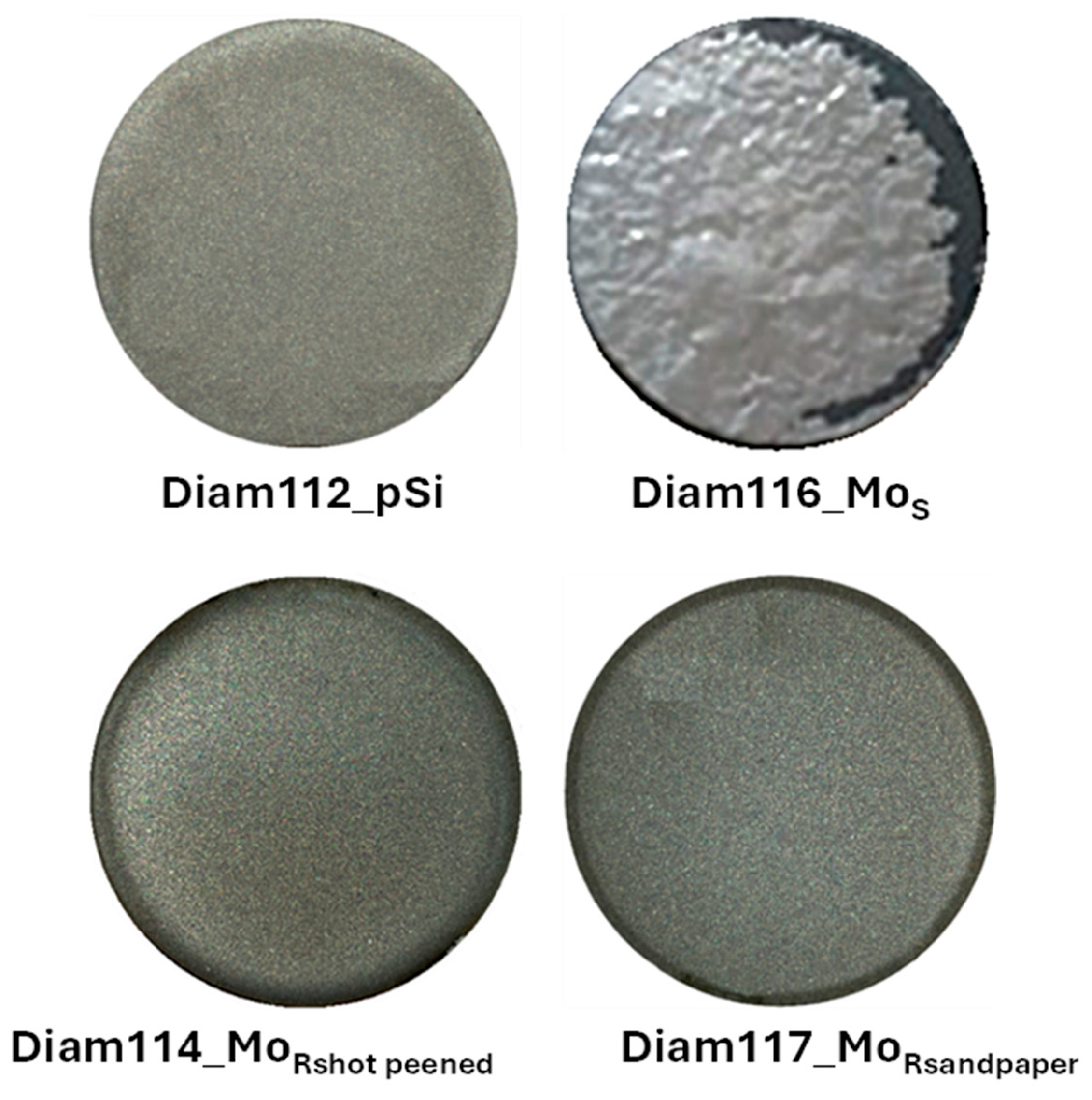
Figure 9.
Photos of the diamond films deposited on p-Si and Mo substrates after 5 days of exposure in air (constant ambient temperature of 22 °C with stable humidity levels of about 65%).
Figure 9.
Photos of the diamond films deposited on p-Si and Mo substrates after 5 days of exposure in air (constant ambient temperature of 22 °C with stable humidity levels of about 65%).
Raman spectra of diamond films are reported in Figure 10 and confirm the results obtained by XRD and SEM analyses. The films exhibit typical features of micro- and nano-crystalline diamond films [31]. In particular, Diam112_pSi spectrum shows a typical microcrystalline structure with a diamond peak at 1332 cm-1 and the G-band centered at 1515 cm-1 due to graphite and sp2 bonds at grain boundaries.
Small changes are beginning to be seen in Diam116_MoS spectrum: the diamond peak is positioned at 1331.9 cm-1 but a peak is beginning to be seen at 1480 cm-1 due to the trans-polyacetylene (t-PA). The structural properties of this film are different from Diam112_pSi and exhibit both microcrystalline and nanocrystalline characters.
The spectra of Diam114_MoRshot-peened and Diam117_MoRsandpaper appear similar, but different from Diam112_pSi and Diam116_MoS. They show the diamond peak shifted to more than 1336 cm-1 and a more prominent t-PA peak at 1480 cm-1.
The shift, from the 1332 cm-1 literature value to 1336 cm-1, is generally attributed to a structural stress in the films (discussed below).
In terms of the diamond peak width (FWHM), there is also a difference between the samples. The lower FWHM values of the diamond peaks of Diam112_pSi and Diam116_MoS indicates a higher microcrystalline nature of these films with respect the others.
In addition, it is easy to observe that going from microcrystalline (Diam116_MoS) to nanocrystalline (Diam114_MoRshot-peened and Diam117_MoRsandpaper) films, the diamond peak decreases and at the same time the graphite band widens and increases because the graphitic component at the grain boundaries increases.
A qualitative estimate of the carbon fraction organized in the diamond or in the graphite structure can be determined via a quality factor (Fq) defined as the ratio Fq=ID/IND, where ID and IND are the peak intensities of the diamond peak and the graphite band, respectively. Similarly, one can consider the ratio AR=AD/AND where AD and AND are the areas of the diamond peak and the graphite band, respectively. High values of Fq or AR ratios indicate a microcrystalline nature of the films. Table 5 reports these data obtained by analyzing the Raman spectra; the reported values are the average over four different points for each sample analyzed.
All these results evidence how the structural characteristic of diamond films deposited on molybdenum is closely related to the surface roughness of the substrate: a smooth Mo surface favors the growth of a film with a microcrystalline character, while both rough Mo surfaces (roughness approximately 10 times that of smooth Mo) favor the growth of a nanocrystalline film.
From Raman spectra, it is possible to obtain further information on diamond films grown on Mo substrates. In particular, the shift of the diamond peak can be related to the residual stress of the deposited film [32]. This stress was calculated by the following equation [32,33]:
were 0.49 GPa/cm-1 is the weighted average gauge factor related to a polycrystalline diamond film, m is the Raman shift of the deposited diamond film and 0 is the position of diamond peak without stress condition.
Table 6 reports the residual stress values obtained by eq. (4): for the diamond grown on smooth Mo (Diam116_MoS) a very low but positive value of 0.05 GPa is found, which means tensile stress (can cause cracking or peeling) in according with its microcrystalline character, whereas the two nanocrystalline films deposited on rough Mo (Diam114_MoRshot-peened and Diam117_MoRsandpaper) show negative values i.e. compressive stress (pushes the film inward and can lead to wrinkling or buckling), as expected [32].
Table 6 also shows the thermal and the intrinsic stresses; their sum gives the total residual stress. Intrinsic stress refers to the internal stresses in deposited thin films that arise during the growth process and it is generally influenced by process parameters such as gas pressure in the deposition chamber and substrate temperature [34].
The thermal stress, related to the thermal expansion between film and substrate, was calculated by the following formula:
where the subscripts “DIAM” and “SUB” indicate diamond and substrate respectively, is the coefficient of thermal expansion, T and T0 are the deposition and room temperatures respectively, t is the thickness, is the Poisson’s ratio and E is the Young’s modulus.
Figure 11 shows the stresses (expressed in absolute value) of the films deposited on molybdenum together with the roughness of their substrate: a trend closely related to the thermal stress (i.e. deposition temperature) and the roughness of the Mo substrate can be observed, i.e. they are inversely proportional.
As can be easily seen from Figure 11, the diamond film deposited on smooth Mo shows the highest values of thermal and intrinsic stresses. The intrinsic (growth) stress affects the grain size, growth rate and deposited energy. Conversely, thermal stress is closely related to deposition temperature and can induce deformations in thin films, such as bending and warping, and can even lead to fracture and delamination (as observed in Diam116_MoS). Film growth at high temperatures tends to produce tensile stresses and promotes grain growth and high deposition rates. This is one of the reasons why Diam116_MoS film has a microcrystalline character, higher deposition rates compared to the other films deposited on rough Mo (see Table 1) and tensile stress.
4. Preliminary Tests on Cathode Erosion in Plasma
The ultimate purpose of these diamond films is to be able to use them as neutralizing cathodes for aerospace propulsion. Conventional neutralizers exploit thermionic electron emission of materials with low or negative work function. These conventional neutralizers rely on the surface properties of the material and their interactions with the plasma and working gas and are prone to cathode poisoning. The poisoning process causes an increase in the work function of the thermionic emitter and consequently a decrease in electron emission. Plasma cathodes have been considered as a potential replacement to conventional hollow cathodes [35] since they do not rely on a thermionic emissive material and, instead, rely on ionization and electron generation in the bulk plasma.
It follows that the stability of the diamond films and their adhesion to the substrate is a key parameter, since a cathode is exposed to harsh working conditions, such as high temperature and wear due to the plasma produced during thrust.
In order to see how these diamond films behave under the action of plasma, erosion tests using an Ar plasma (this is one of the gases used as a propellant) in an RF sputtering reactor was investigated. Aware that the present experimental conditions did not represent those experienced during aerospace propulsion, the aim at this preliminary stage was simply to study the degradation of diamond films under plasma interaction.
In this section, preliminary results obtained by exposing three diamond samples, freshly deposited on three different Mo substrates and synthesized under the same conditions are shown.
They were mounted on the substrate holder of a sputtering chamber. Ar gas (P = 2x10⁻³ mbar) was introduced into the chamber through a mass flow controller and an RF biasing (13.56 MHz) was applied to the substrate. The applied RF power (300 W) created a negative DC voltage on the substrate (equal to about – 400 V) that accelerated Ar ions across the plasma-substrate sheath, bombarding the diamond film surface.
Figure 12 reports the photos of the cathodes after the plasma treatment (Figs. 12b). SEM images showed the areas where diamond films exhibited less erosion and were more intact (Figs. 12a).
It is evident from Figure 12b that the least stable film is once again the one deposited on smooth Mo. On the contrary, the most stable film (among those deposited on Mo substrates) was Diam114_MoRshot-peened. It appeared that a “more uniform” roughness of the substrate surface improved adhesion as it reduces the process temperature (i.e. intrinsic and thermal stresses, as evident in Fig. 11)) compared to a smooth or unevenly rough surface, such as that obtained with sandpaper.
In conclusion, the results obtained in this work demonstrate that:
- a rough substrate surface is better than a smooth one for the growth of diamond films on molybdenum by MWPECVD technique;
- the use of a rough Mo substrate reduces the deposition temperature (TD);
- the decrease in TD results in lower thermal and intrinsic stresses;
- the decrease in TD also leads to a change in the stress of the films, switching from tensile stresses to compressive stresses (from microcrystalline to nanocrystalline film character), limiting cracking or peeling phenomena attributed to tensile stress;
- more uniform substrate roughness improves films stability and further reduces the deposition temperature with the consequent above mentioned advantages.
5. Conclusions
The influence of the molybdenum substrates roughness on the characteristics of diamond films has been discussed based on AFM, SEM, XRD, and Raman results. Specifically, the roughened Mo substrates guarantee a higher mechanical stability of the films without delamination. This result was further confirmed during our plasma test where silicon and roughened Mo substrates do not show mechanical failure. This was probably due to the lower values of thermal and intrinsic stresses of these two films with respect to the one deposited on smooth Mo.
Moreover, these results have shown how the values of deposition temperature are correlated with diamond-substrate adhesion. The adhesion was good for the film deposited on silicon, whose minima and maxima of interference fringes of the pyrometric interferogram and deposition temperature were within the measurement range of the pyrometer (475 °C < T <1475°C) and of 820 °C. As for Mo substrates, the roughness and therefore the morphology have affected the adhesion and the structural properties of diamond film. In fact, it was found an undefined high deposition temperature >950 °C for films deposited on smooth Mo substrate because the pyrometric interferogram showed minima and maxima values of the interference fringes below 475 °C and above 1475 °C, outside of the pyrometer’s measurement range. Such a high temperature (>950 °C) caused a change in structure of diamond (from nano- to micro- crystalline), higher thermal and intrinsic stresses, higher residual strain and consequently the poor adhesion of the film to the substrate and the detachment of the film itself. Instead, the diamond films on roughened Mo substrates, Diam114_MoRshot-peened and Diam117_MoRsandpaper, were well adherent, stable with lower deposition temperature of 818 and 873 °C, respectively. In particular, Diam114_MoRshot-peened showed the best mechanical stability and adhesion among the films deposited on Mo, thanks to the method used to treat the Mo substrate (shoot peening), which allows for a uniform and controlled increase in surface roughness, causing the film to grow at lower temperatures and thus reducing thermal and intrinsic stresses compared to that grown under the same experimental conditions but on a smoother surface.
These results were confirmed by preliminary erosion tests in plasma environment, where the most stable film (among those deposited on Mo substrates) was Diam114_MoRshot-peened. It appeared that a “more uniform” roughness of the substrate surface improved adhesion as it reduces intrinsic and thermal stress compared to a smooth or unevenly rough surface, such as that obtained with sandpaper.
Moreover, the support of the process diagnostics like pyrometric interferometry allowed to predict the adhesion and the stability of diamond films before their exposure in air. This is a very interesting aspect that has never been addressed in research papers, as pyrometric interferometry was generally used to assess the rate and the temperature of deposition, and not to study the quality of the thin films and their adhesion to the substrate. Thus, it was possible to define the stability of the diamond film already during the growth process by simply monitoring the pyrometric interferograms i.e. the apparent and deposition temperatures.
Author Contributions
Conceptualization, L.V. and G.C.; methodology, L.V and M.A.S.; software, L.V.; validation, L.V., M.A.S., G.C. and L.N.F.; investigation, L.V., G.C. and M.A.S.; resources, G.C. and L.N.F.; data curation, L.V and M.A.S.; writing—original draft preparation, L.V., M.A.S. and G.C.; supervision, L.V., M.A.S., G.C. and L.N.F. All authors have read and agreed to the published version of the manuscript.
Funding
This research received no external funding.
Institutional Review Board Statement
Not applicable.
Informed Consent Statement
Not applicable.
Data Availability Statement
The original contributions presented in this study are included in the article. Further inquiries can be directed to the corresponding author.
Conflicts of Interest
The authors declare no conflicts of interest.
Abbreviations
The following abbreviations are used in this manuscript:
| CVD | Chemical Vapor Deposition |
| HFCVD | Hot Filament Chemical Vapor Deposition |
| MWPECVD | Microwave Plasma Enhanced Chemical Vapor Deposition |
| PI AFM XRD SEM PID FWHM RF |
Pyrometric Interferometry Atomic Force Microscopy X Ray Diffraction Scanning Electron Microscopy Proportional Integral Derivative Full Width at Half Maximum Radio Frequency |
References
- Mckeag, R.D.; Chan, S.S.M.; Jackman, R.B. Polycrystalline diamond photoconductive device with high UV-visible discrimination. Appl. Phys. Lett. 1995, 67, 2117. [Google Scholar] [CrossRef]
- Muscarella, M.F.; Altamura, D.; Brescia, R.; Capitelli, M.; Casamassima, G.; Cassano, T.; Celiberto, R.; Cicala, G.; Cornacchia, D.; De Giacomo, A.; De Pascale, O.; Favuzzi, C.; Ferraro, G.; Fusco, P.; Gargano, F.; Giglietto, N.; Giordano, F.; Gorse, C.; Longo, S.; Loparco, F.; Magaletti, V.; Marangelli, B.; Mazziotta, M.N.; Monéger, D.; Nitti, M.A.; Rainò, A.; Romeo, A.; Senesi, G.; Spinelli, P.; Valentini, A.; Velardi, L. A comparative study on comb electrodes devices made of MWPECVD diamond films grown on p-doped and intrinsic silicon substrate. Diam. Relat. Mater. 2011, 20, 1005–1009. [Google Scholar] [CrossRef]
- Velardi, L.; Valentini, A.; Cicala, G. Highly efficient and stable photocathode based on nanodiamond particles. Appl. Phys. Lett. 2016, 108, 083503. [Google Scholar] [CrossRef]
- Jou, S.; Huang, B-R.; Wu, M.-C.; Nanocrystalline diamond film as cathode for gas discharge sensors. Thin Solid Films 2010, 518, 4458–4461. [CrossRef]
- Cicala, G.; Nitti, M.A.; Tinti, A.; Valentini, A.; Romeo, A.; Brescia, R.; Spinelli, P.; Capitelli, M. Effect of properties of MWPECVD polycrystalline diamond films on photoemissive response. Diam. Relat. Mater. 2011, 20, 1199–1203. [Google Scholar] [CrossRef]
- Cicala, G.; Magaletti, V.; Valentini, A.; Nitti, M.A.; Bellucci, A.; Trucchi, D.M. Photo- and thermionic emission of MWPECVD na-nocrystalline diamond films. Appl. Surf. Sci. 2014, 320, 798–803. [Google Scholar] [CrossRef]
- Agarwala, J.; Chatterjee, C.; Cicala, G.; Cicuttin, A.; Ciliberti, P.; Crespo, M.L.; Dalla Torre, S.; Dasgupta, S.; Gregori, M.; Levorato, S.; Menon, G.; Tessarotto, F.; Valentini, A.; Velardi, L.; Zhao, Y. Study of MicroPattern Gaseous detectors with novel nanodiamond based photocathodes for single photon detection in EIC RICH. Nucl. Instrum. Methods Phys. Res. A: Accel. Spectrom. Detect. Assoc. Equip. 2020, 952, 161967. [Google Scholar] [CrossRef]
- Wang, Y.; Lin, C.; Zhang, J. High performance field emission cathode based on the diamond nanowires prepared by nanocrystalline diamond films annealed in air. J. Micromech. Microeng. 2024, 34, 025011. [Google Scholar] [CrossRef]
- Wang, W.L.; Liao, K.J.; Fang, L.; Esteve, J.; Polo, M.C. Analysis of diamond nucleation on molybdenum by biased hot filament chemical vapor deposition, Diam. Relat. Mater. 2001, 10, 383–387. [Google Scholar] [CrossRef]
- Cicala, G.; Velardi, L.; Senesi, G.S.; Picca, R.A.; Cioffi, N. Electrical current at micro-/macro-scale of undoped and nitrogen-doped MWPECVD diamond films. Appl. Surf. Sci. 2017, 426, 456–465. [Google Scholar] [CrossRef]
- Köpf, A.; Lux, B.; Haubner, R. Substrate Effects during Nucleation and Growth of CVD diamond, 2001, 11, 11-23. New Diamond and Frontier Carbon Technology 2001, 11, 11–23. [Google Scholar]
- Behera, M.; Jena, A.; Pattnaik, S.K.; Padhi, S.; Sarangi, S.K. The effect of transition-metal seeding powder on deposition and growth of diamond synthesized by hot filament chemical vapor deposition processes on cemented carbide substrates and its characterization. Mater. Chem. Phys. 2020, 256, 123638. [Google Scholar] [CrossRef]
- Stoner, B.R.; Ma, G.H.M.; Wolter, S.D.; Glass, J.T. Characterization of bias-enhanced nucleation of diamond on silicon by invacuo surface analysis and transmission electron microscopy, Phys. Rev. B 1992, 45, 11067. [Google Scholar] [CrossRef] [PubMed]
- Meilunas, R.; Wong, M.S.; Sheng, K.C.; Chang, R.P.H.; Van Duyne, R.P. Early stages of plasma synthesis of diamond films. Appl. Phys. Lett. 1989, 54, 2204. [Google Scholar] [CrossRef]
- Jubber, G.; Milne, D.K. Microwave Plasma CVD of High Quality Heteroepitaxial Diamond Films. Phys. Status Solidi A 1996, 154, 185. [Google Scholar] [CrossRef]
- Lux, B.; Haubner, R. Diamond substrate interactions and the adhesion of diamond coatings. Pure Appl. Chem. 1994, 66, 1783–1788. [Google Scholar] [CrossRef]
- Ashfold, M.N.R.; May, P.W.; Rego, C.A.; Everitt, N.M. Thin film diamond by chemical vapour deposition methods. Chem. Soc. Rev. 1994, 23, 21–30. [Google Scholar] [CrossRef]
- Trava-Airoldi, V.J.; Corat, E.J.; Santos, L.V.; Moro, J.R.; Leite, N.F. Studies of molybdenum surface modification for growth of adherent CVD diamond Films. Materials Research 2003, 6, 305–309. [Google Scholar] [CrossRef]
- Buijnsters, J.G.; Shankar, P.; van Enckervort, W.J.P.; Schermer, J.J.; ter Meulen, J.J. Adhesion analisis of polycrystalline diamond films on molybdenum by means of scratch, indentation and sand abrasion testing, Thin Solid Films 2005, 474, 186–196. [Google Scholar] [CrossRef]
- Wako, H.; Abe, T.; Takagi, T.; Ikohagi, T. Comparison of diamond film adhesion on molybdenum substrates with different surface morphologies, Appl. Surf. Sci. 2009, 256, 1466–1471. [Google Scholar] [CrossRef]
- Ristić, G.S.; Bogdanov, Ž.D.; Zec, S.; Romčević, N.; Dohčević-Mitrović, Z.; Miljanić, Š.S. Effect of the substrate material on diamond CVD coating properties, Mater. Chem. Phys. 2003, 80, 529–536. [Google Scholar] [CrossRef]
- Mallik, A.K. , Binu, S.R., Satapathy, L.N.; Narayana, C.; Seikh, M.M.; Shivashankar, S.A.; Biswas, S.K. Effect of substrate roughness on growth of diamond by hot filament CVD. Bull. Mater. Sci. 2010, 33, 251–255. [Google Scholar] [CrossRef]
- Mandal, S. ; Nucleation of diamond films on heterogeneous substrates: a review. RSC Adv. 2021, 11, 10159–10182. [Google Scholar] [CrossRef] [PubMed]
- Cicala, G.; Bruno, P.; Bénédic, F.; Silva, F.; Hassouni, K.; Senesi, G.S. Nucleation, growth and characterization of nanocrystalline diamond films. Diam. Relat. Mater. 2005, 14, 421–425. [Google Scholar] [CrossRef]
- Li, X.; He, L.; Li, Y.; Yang, Q. Diamond Deposition on Iron and Steel Substrates: A Review, Micromachines 2020, 11, 719. Micromachines 2020, 11, 719. [Google Scholar] [CrossRef]
- Akatsuka, F.; Shimura, F. Effect of Substrate Materials on CVD diamond Growth. Materials Science Monographs 1991, 73, 379–381. [Google Scholar] [CrossRef]
- Fernandes, A.; Neves, A.; Silva, R.F.; Nazaré, M.H. Evaluation of MPCVD diamond film adhesion on hard metal substrates by micro Raman spectroscopy. Diam. Relat. Mater. 1997, 6, 769–773. [Google Scholar] [CrossRef]
- Cicala, G.; Brescia, R.; Nitti, M. A.; Romeo, A.; Altamura, D.; Giannini, C.; Capitelli, M.; Spinelli, P.; Schutzmann, S. Study of polycrystalline diamond deposition by continuous and pulsed discharges. Surf. Coat. Technol. 2010, 204, 1884–1888. [Google Scholar] [CrossRef]
- Langford, J.I.; Wilson, A.J.C. Scherrer after sixty years: A survey and some new results in the determination of crystallite size. J. Appl. Cryst. 1978, 11, 102–113. [Google Scholar] [CrossRef]
- Williamson, G.K.; Smallman, R.E., III. Dislocation densities in some annealed and cold-worked metals from measurements on the X-ray debye-scherrer spectrum. The Philosophical Magazine: A Journal of Theoretical Experimental and Applied Physics 1956, 1, 34–46. [Google Scholar] [CrossRef]
- Gicquel, A.; Hassouni, K.; Silva, F.; Achard, J. CVD diamond films: from growth to applications. Current Applied Physics 2001, 1, 479–496. [Google Scholar] [CrossRef]
- Long, F.; Wei, Q.; Yu, Z.M.; Luo, J.; Zhang, X.; Long, H.; Wu, X. Effects of temperature and Mo2C layer on stress and structural properties in CVD diamond film grown on Mo foil. J. Alloys Compd. 2013, 579, 638–645. [Google Scholar] [CrossRef]
- Ahmed, F.; Bayerlein, K.; Rosiwal, S.M.; Göken, M.; Durst, K. Stress evolution and cracking of crystalline diamond thin films on ductile titanium substrate: Analysis by micro-Raman spectroscopy and analytical modelling. Acta Mater. 2011, 59, 5422–5433. [Google Scholar] [CrossRef]
- Huff, M. Review Paper: Residual Stresses in Deposited Thin-Film Material Layers for Micro- and Nano-Systems Manufacturing. Micromachines 2022, 13, 2084. [Google Scholar] [CrossRef]
- Gurciullo, A.; Lucca Fabris, A.; Knoll, A. Direct Current Plasma Electron Source for Electric Propulsion Applications Using Atomic and Molecular Propellants. IEEE Trans. Plasma Sci. 2017, 45, 2472–2480. [Google Scholar] [CrossRef]
Figure 1.
a) Photos of molybdenum substrates (2.5 cm of diameter, 0.75 mm of thickness): smooth (MoS), rough by shot peening machine (MoRshot-peened) and rough by sandpaper (MoRsandpaper) and corresponding b) AFM topographies and c) AFM profiles.
Figure 1.
a) Photos of molybdenum substrates (2.5 cm of diameter, 0.75 mm of thickness): smooth (MoS), rough by shot peening machine (MoRshot-peened) and rough by sandpaper (MoRsandpaper) and corresponding b) AFM topographies and c) AFM profiles.
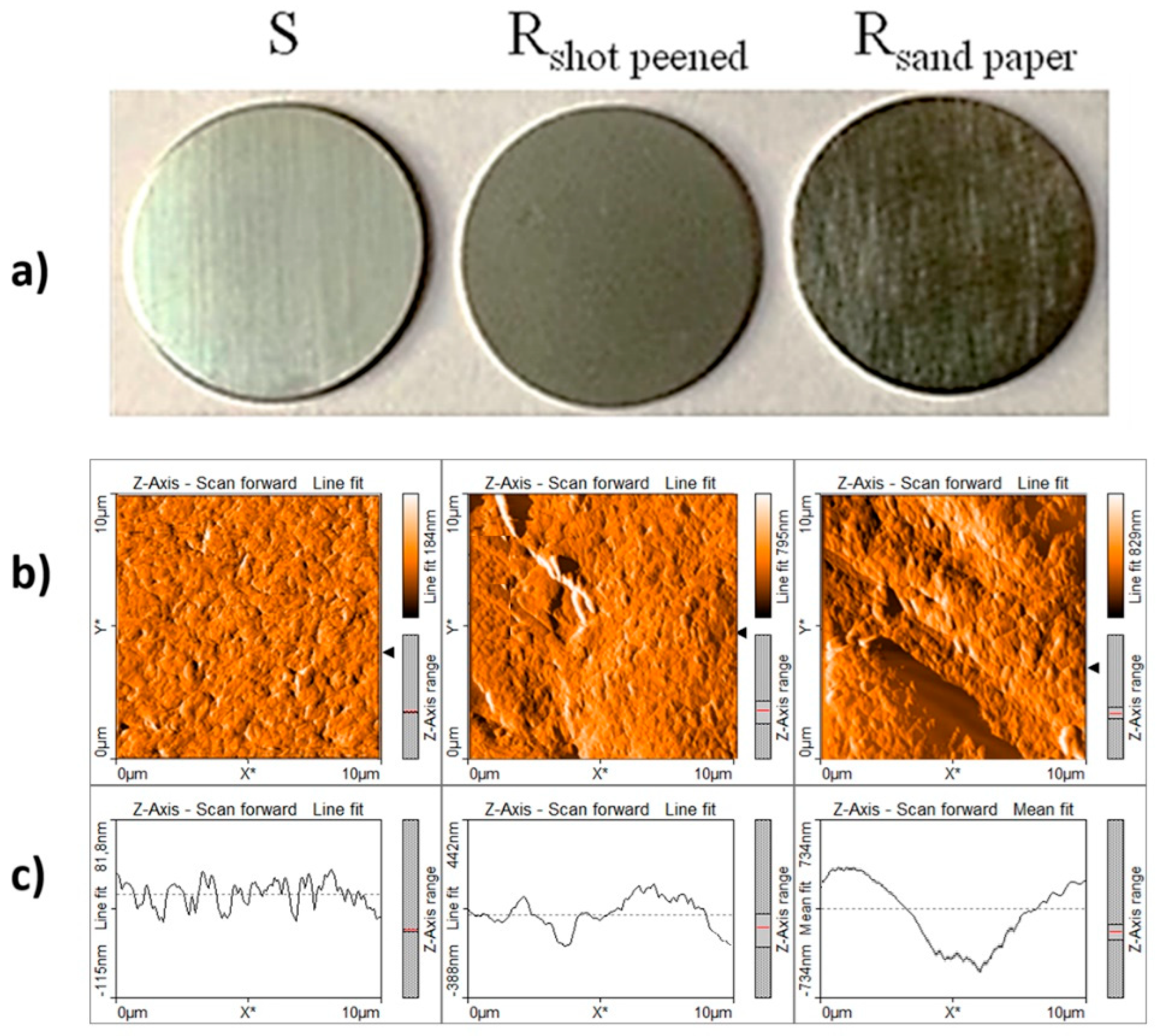
Figure 2.
Trend of the root mean square roughness (Rq) of the substrates, determined by AFM (Nanosurf CoreAFM).
Figure 2.
Trend of the root mean square roughness (Rq) of the substrates, determined by AFM (Nanosurf CoreAFM).
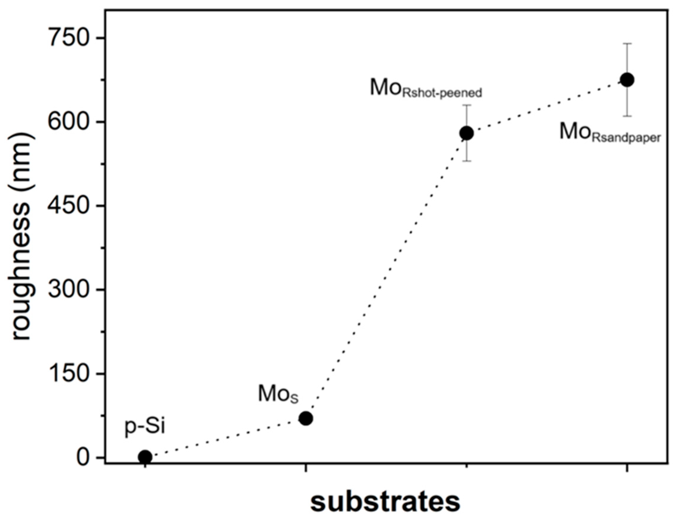
Figure 3.
pyrometric interferograms obtained during the deposition process of Diam116 on smooth Mo (Diam116_MoS, red curve) and of Diam112 on polished p-doped silicon (Diam112_pSi, blue curve).
Figure 3.
pyrometric interferograms obtained during the deposition process of Diam116 on smooth Mo (Diam116_MoS, red curve) and of Diam112 on polished p-doped silicon (Diam112_pSi, blue curve).
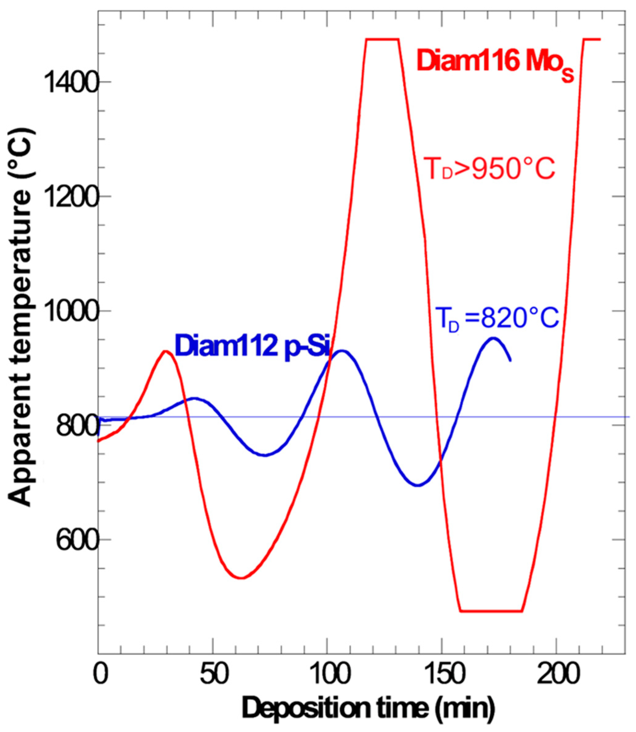
Figure 4.
pyrometric interferograms obtained during the deposition process of Diam116 on smooth Mo (Diam116_MoS, red curve) and of Diam117 on rough Mo by sandpaper (Diam117_MoRsandpaper, blu curve).
Figure 4.
pyrometric interferograms obtained during the deposition process of Diam116 on smooth Mo (Diam116_MoS, red curve) and of Diam117 on rough Mo by sandpaper (Diam117_MoRsandpaper, blu curve).
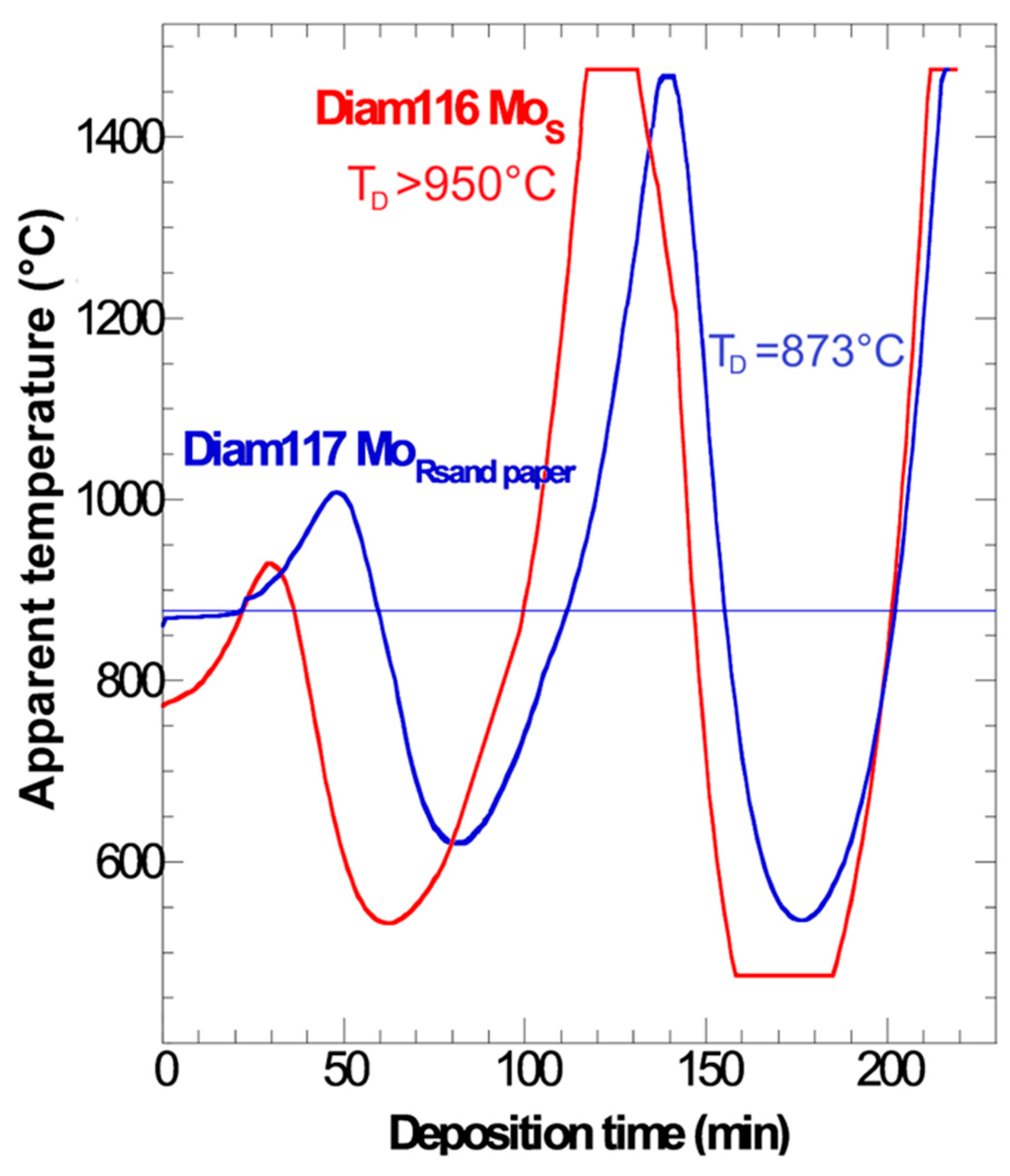
Figure 5.
pyrometric interferograms obtained during the deposition process of Diam116 on smooth Mo (Diam116_MoS, red curve) and of Diam114 on rough shot peened Mo (Diam114_MoRshot-peened, blue curve).
Figure 5.
pyrometric interferograms obtained during the deposition process of Diam116 on smooth Mo (Diam116_MoS, red curve) and of Diam114 on rough shot peened Mo (Diam114_MoRshot-peened, blue curve).
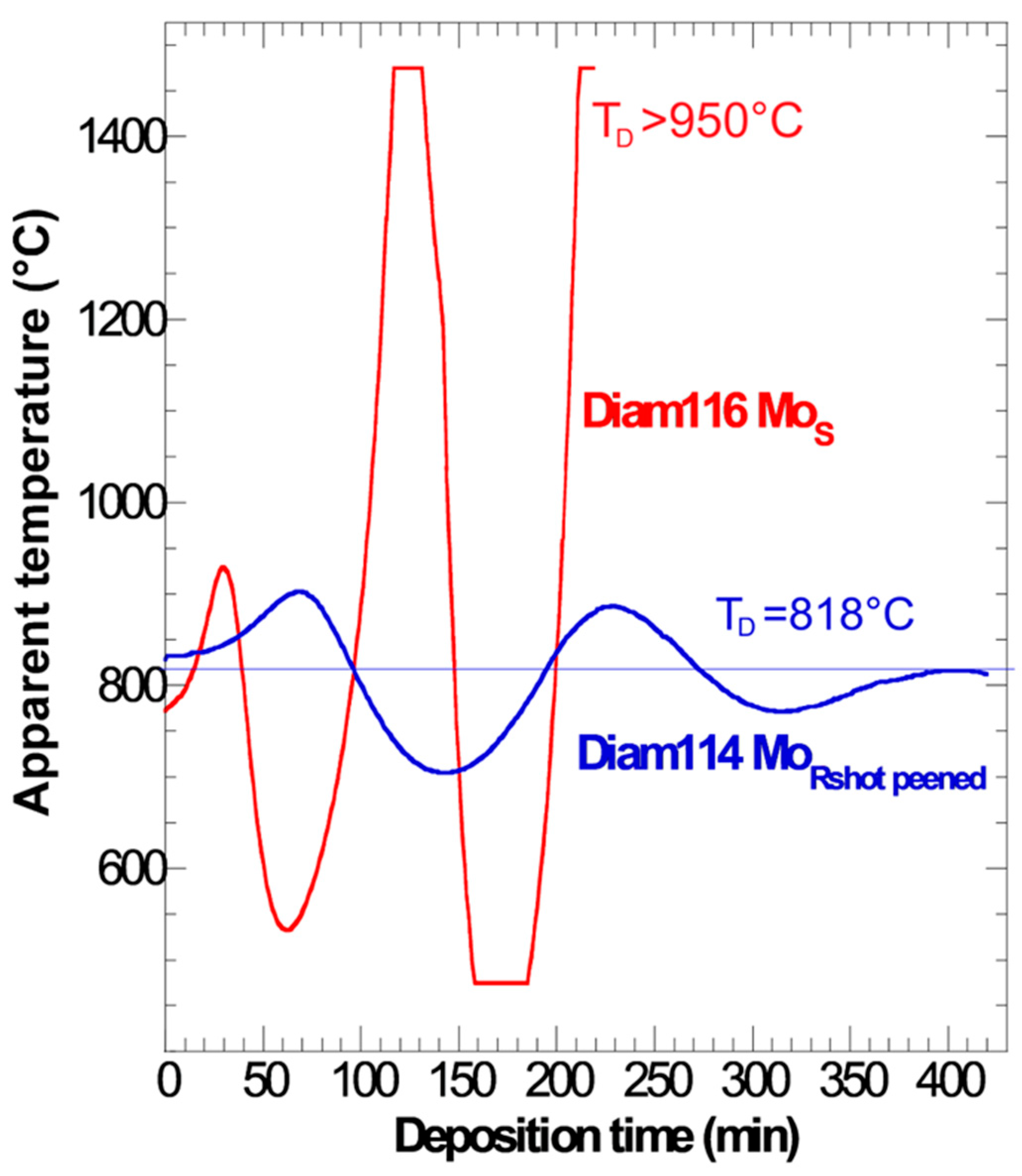
Figure 6.
XRD patterns of the investigated diamond films and Mo substrate.
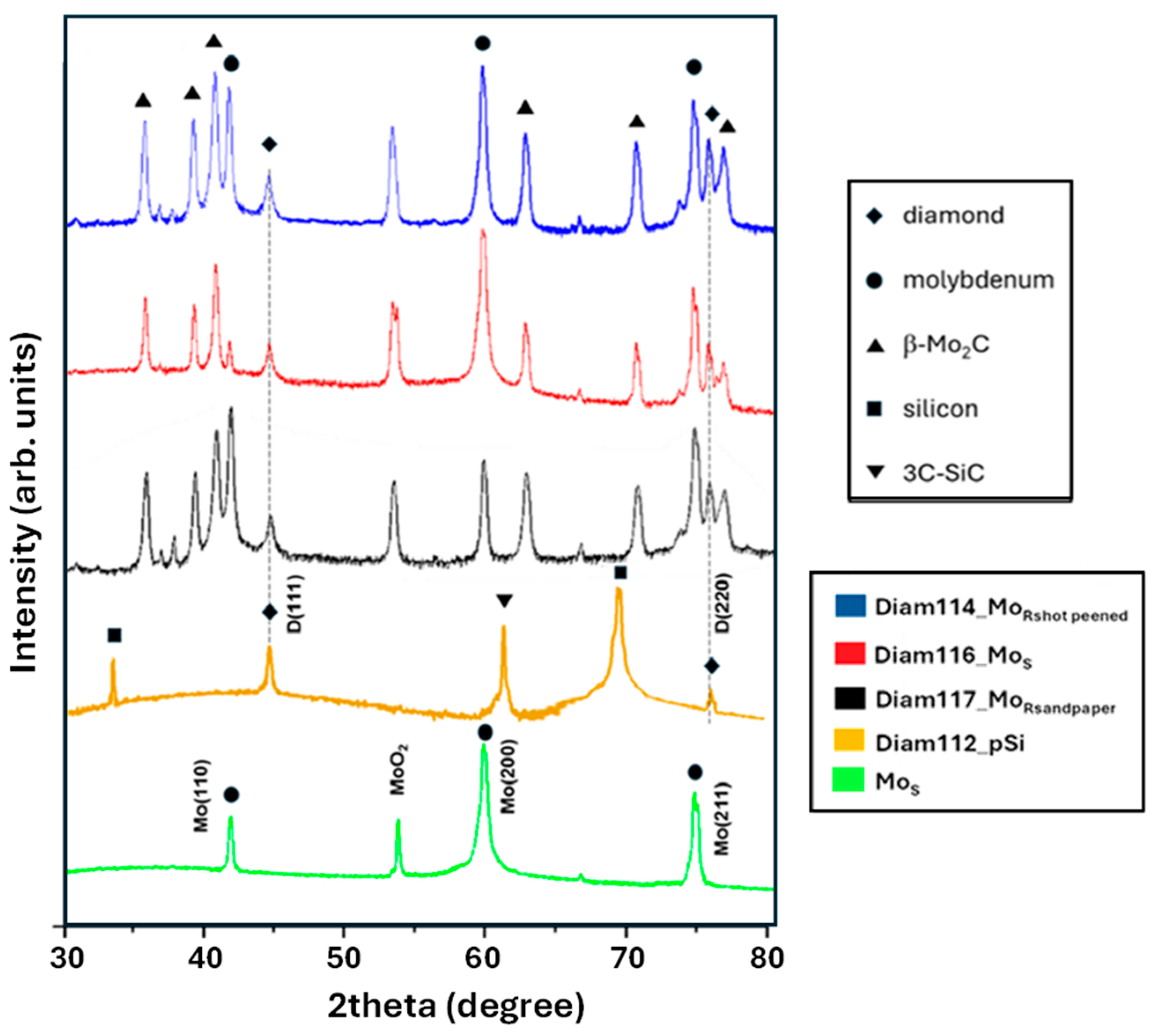
Figure 7.
Substrate roughness Rq vs grain size estimated by XRD spectra.
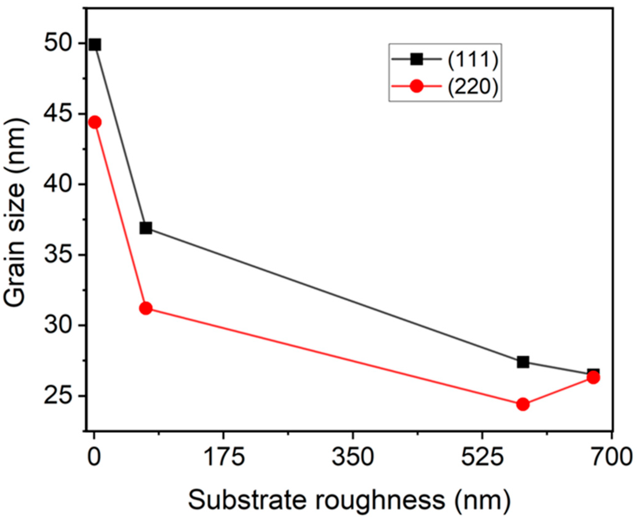
Figure 8.
SEM images of the diamond films deposited on a) p-Si (Diam112_pSi), b) smooth Mo (Diam116_MoS), c) Mo roughened by shot peening (Diam114_MoRshot-peened) and d) Mo roughened by sandpaper (Diam117_MoRsandpaper).
Figure 8.
SEM images of the diamond films deposited on a) p-Si (Diam112_pSi), b) smooth Mo (Diam116_MoS), c) Mo roughened by shot peening (Diam114_MoRshot-peened) and d) Mo roughened by sandpaper (Diam117_MoRsandpaper).
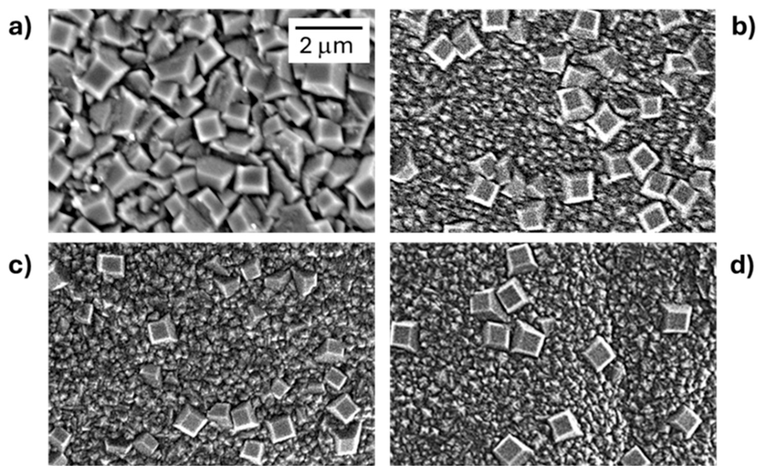
Figure 10.
Raman spectra of diamond films deposited on Si and Mo substrates.
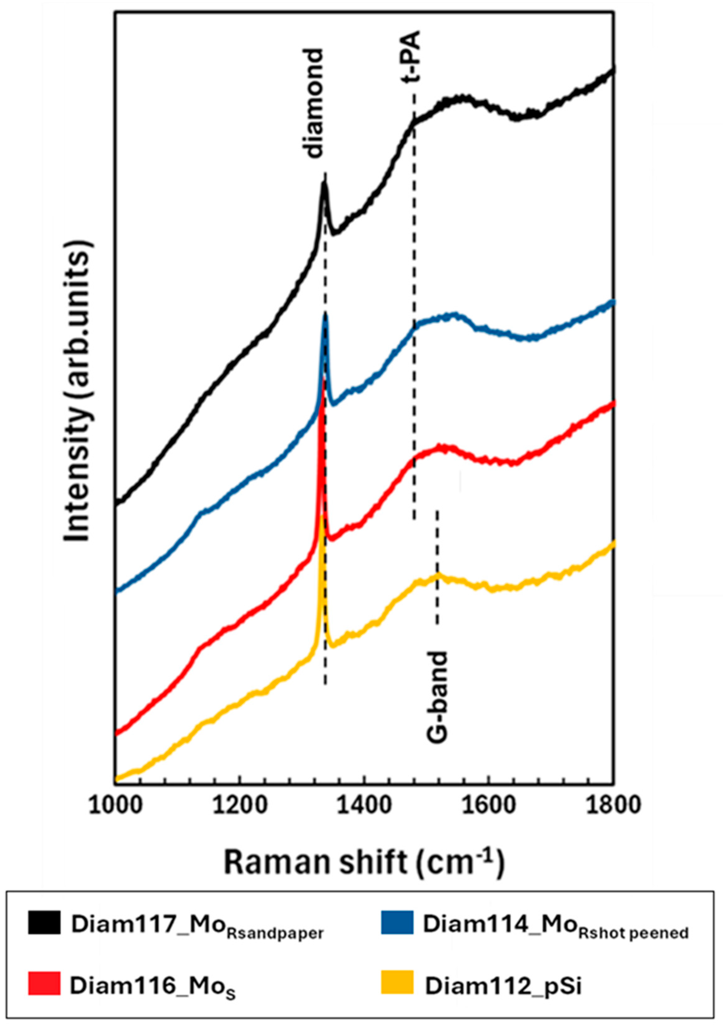
Figure 11.
Stresses (expressed in absolute value) of the diamond films deposited on Mo substrates having different roughness compared with substrate roughness.
Figure 11.
Stresses (expressed in absolute value) of the diamond films deposited on Mo substrates having different roughness compared with substrate roughness.
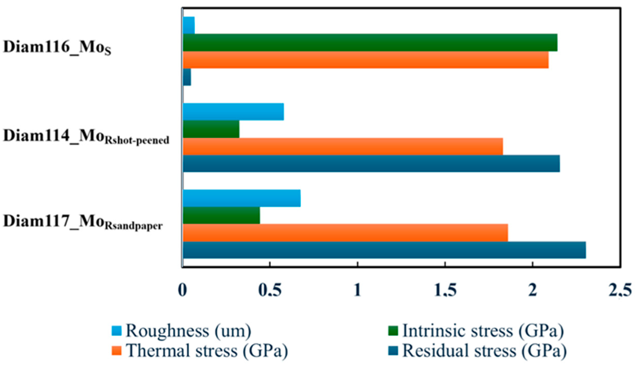
Figure 12.
a) photos of the cathodes after the plasma treatment, b) SEM images showing the areas where diamond films show less erosion and are more intact.
Figure 12.
a) photos of the cathodes after the plasma treatment, b) SEM images showing the areas where diamond films show less erosion and are more intact.
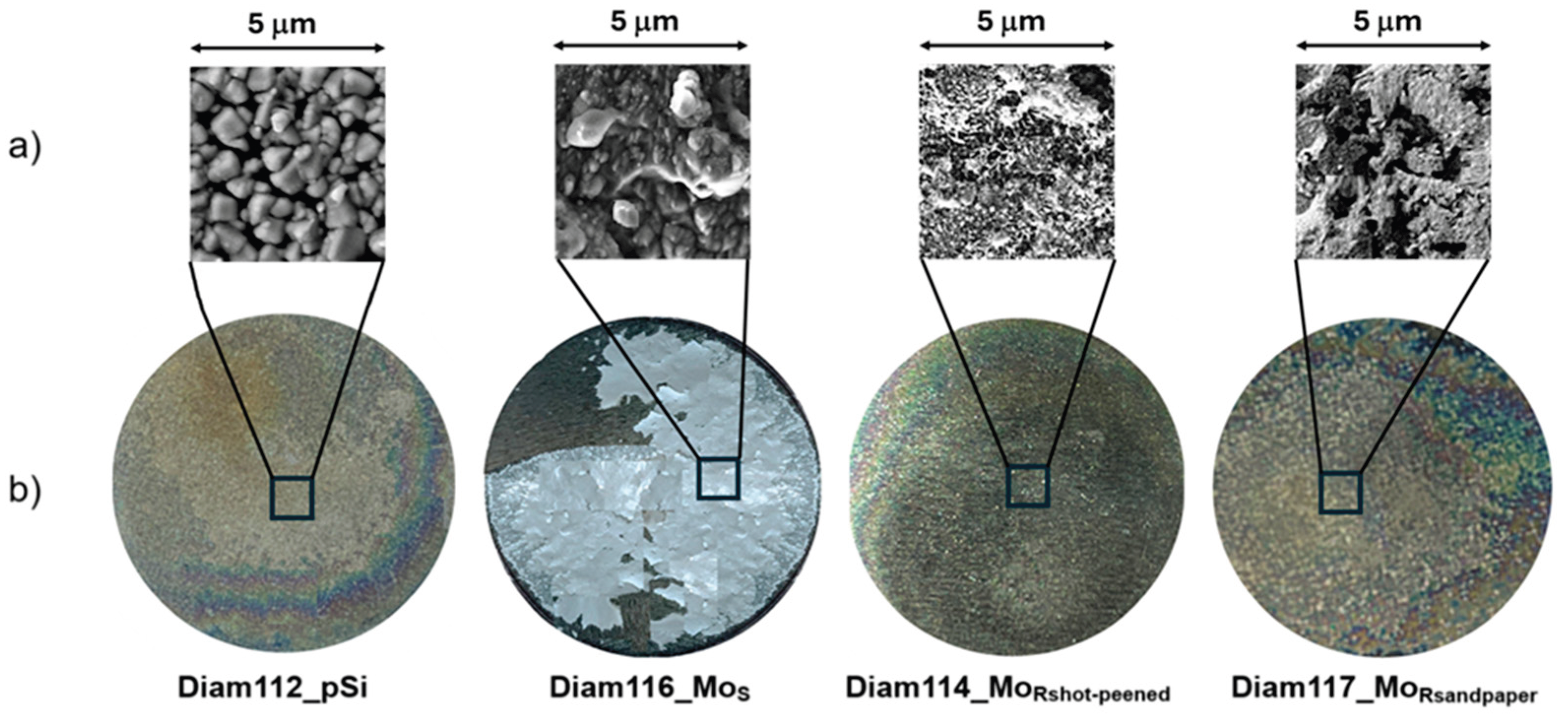

Table 1.
Main properties of substrates suitable to diamond film growth and compared to diamond ones.
Table 1.
Main properties of substrates suitable to diamond film growth and compared to diamond ones.
| Material | Thermal expansion (x 10-6 K-1) | Melting point (°C) | Lattice constant (nm) |
| Copper | 16.5 | 1084 | 0.361 |
| Silicon | 2.6 | 1414 | 0.543 |
| Molybdenum | 4.8 | 2623 | 0.314 |
| Diamond | 1.0 | 4090 | 0.357 |
Table 2.
Plasma conditions for the deposition of diamond films onto silicon p-Si(100) and molybdenum substrates, holding constant the total flow rate (250 sccm), the composition (1 % CH4) of gaseous CH4-H2 mixture, the pressure (35 mbar), the microwave power (1250 Watt) and the heating temperature of susceptor (700 °C).
| Sample | Substrate type |
Deposition temperature (°C) |
Deposition time (min) | Deposition rate rD (μm/h) | thickness (μm) |
| Diam112_pSi | p-Si | 820 | 180 | 0.43 ± 0.01 | 1.29 ± 0.03 |
| Diam116_MoS | smooth Mo | >950 | 219 | 0.33 ± 0.01 | 1.20 ± 0.02 |
| Diam117_ MoRsandpaper | rough Mo1 | 873 | 217 | 0.30 ± 0.01 | 1.10 ± 0.01 |
| Diam114_MoRshot-peened | rough Mo2 | 818 | 420 | 0.17 ± 0.01 | 1.20 ± 0.03 |
1roughened by sandpaper. 2roughened by shot peening.
Table 3.
Grains size (Gs) along (111) and (220) planes of diamond, calculated by Scherrer formula.
| Sample | GS(111) (nm) | GS(220) (nm) | Roughness (nm) |
| Diam112_pSi | 49.9 | 44.4 | very low (< 1) |
| Diam116_MoS | 36.9 | 31.2 | 70 ± 5 |
| Diam114_MoRshot-peened | 27.4 | 24.4 | 580 ± 50 |
| Diam117_MoRsandpaper | 26.5 | 26.3 | 675 ± 65 |
Table 4.
Crystallographic parameters of diamond films obtained by XRD analysis.
| Sample |
a (111) Å |
a (220) Å |
δ111 (×1015lines/m2) |
δ220 (×1015lines/m2) |
Ν111 (×1016/m2) |
Ν220 (×1016/m2) |
| Diam112_pSi | 3.54 | 3.55 | 0.40 | 0.51 | 1.04 | 1.48 |
| Diam116_MoS | 3.50 | 3.51 | 0.73 | 1.02 | 2.80 | 4.62 |
| Diam114_MoRshot-peened | 3.51 | 3.52 | 1.33 | 1.68 | 5.78 | 8.20 |
| Diam117_MoRsandpaper | 3.51 | 3.52 | 1.42 | 1.45 | 7.16 | 7.35 |
Table 5.
Diamond peak, FWHM, t-PA, G-band, Fq, and AR data obtained by analyzing the Raman spectra.
| Sample | Diamond peak (cm-1) | FWHM (cm-1) |
t-PA (cm-1) |
G-band (cm-1) |
Fq=ID/IND | AR=AD/AND |
| Diam112_pSi | 1332.0 | 4.8 | -- | 1515 | 7.0 | 0.45 |
| Diam116_MoS | 1331.9 | 5.3 | 1485 | 1515 | 4.4 | 0.28 |
| Diam114_MoRshot-peened | 1336.7 | 8.1 | 1485 | 1545 | 1.8 | 0.17 |
| Diam117_MoRsandpaper | 1336.4 | 10.0 | 1493 | 1555 | 1.3 | 0.14 |
Table 6.
Stresses values of the diamond films on Mo substrates.
| Sample | Residual stress (GPa) | Thermal stress (GPa) | Intrinsic stress (GPa) | Diamond peak (cm-1) |
| Diam116_MoS | 0.05 | -2.09 | 2.14 | 1331.9 |
| Diam114_MoRshot-peened | -2.16 | -1.83 | -0.32 | 1336.4 |
| Diam117_MoRsandpaper | -2.30 | -1.86 | -0.44 | 1336.7 |
Disclaimer/Publisher’s Note: The statements, opinions and data contained in all publications are solely those of the individual author(s) and contributor(s) and not of MDPI and/or the editor(s). MDPI and/or the editor(s) disclaim responsibility for any injury to people or property resulting from any ideas, methods, instructions or products referred to in the content. |
© 2025 by the authors. Licensee MDPI, Basel, Switzerland. This article is an open access article distributed under the terms and conditions of the Creative Commons Attribution (CC BY) license (http://creativecommons.org/licenses/by/4.0/).
Copyright: This open access article is published under a Creative Commons CC BY 4.0 license, which permit the free download, distribution, and reuse, provided that the author and preprint are cited in any reuse.


