
Submitted:
17 September 2025
Posted:
19 September 2025
You are already at the latest version
Abstract
The Zeta converter has many interesting features. The main switch is in series to the positive terminal of the input source. So no inrush occurs, when the converter is connected to the supply and it can be used as an electronic fuse in case of an error. The output side of the converter is an LC-filter, so only the current ripple of the current through the output coil is flowing through the output capacitor, and the voltage across it is very stable, even with a smaller capacitor. To reduce the switching losses and to smooth the slope of the signals, the zero current switching (ZCS) and the zero voltage switching (ZVS) can be applied. The converter must be extended by a small resonant inductor in series to the electronic switch and a capacitor in parallel (in case of ZVS) to the electronic switch or in parallel to the diode (in case of ZCS). The function of the converter is explained in detail with the help of calculations and with the u-Zi diagram. The considerations are proved with the help of LTSpice simulations. The Sepic and the Cuk converter are also treated as QR converters.
Keywords:
DC/DC converter
; zero current switching (ZCS)
; zero voltage switching (ZVS)
; Zeta
; Sepic
; Cuk
; quasi resonant (QR)
1. Introduction
The idea of constructing quasi resonant (QR) converters has its origin in papers by K.-H. Liu and F.C. Lee. The concept is explained with the help of the Boost converter and the topologies of a family of converters are depicted in [1]. The QR Buck converter is explained and a family of QR converters can be found in [2]. A concept for the syntheses of QR converters based on graph theory is shown in [3]. QR topologies, including the forward and the flyback converters, are shown in [4]. A ZVS Zeta for high frequencies and for generating two output voltages is treated in [5]. A comprehensive reliability assessment of the QR Buck converter is given in [6]. An adaption of a QR converter between a power interface and an inverter for driving an induction machine is used in [7]. A theoretical method to study transients in QR converters is explained for a Buck converter in [8]. One drawback of the QR concept is that it should be used for not too large changing outside parameters. This is treated for the Boost converter in [9]. A ZVS QR Boost converter is studied by using the simulation tool Matlab/Simulink in [10]. Starting from the Boost converter, a QR converter for photovoltaic application is studied in [11]. The effect of reducing the electromagnetic interference (EMI) of a DC/DC converter, when using the QR, is shown in [12]. An interesting combination of data transmission and power conversion is treated in [13]. There a Buck converter is used. A ZCS Boost converter is studied with the state-plane in [14]. A method to get constant switching frequency for a QR converter, demonstrated with a Boost converter, is proposed in [15]. A QR flyback converter, which switches not at zero but at a low value, which is detected by a special circuit, is explained in [16]. A comprehensive study concerning Cuk, Zeta and Sepic converters can be found in [17]. The application of the ZVS QR concept on the modified Boost converter is demonstrated in [18]. It should be mentioned that all pulse width modulated (pwm) DC/DC converters with one switch can be changed easily into QR converters. The basic converters are discussed in all textbooks on Power Electronics, e.g. [19,20,21].
1.1. The Zeta Converter in the Steady State
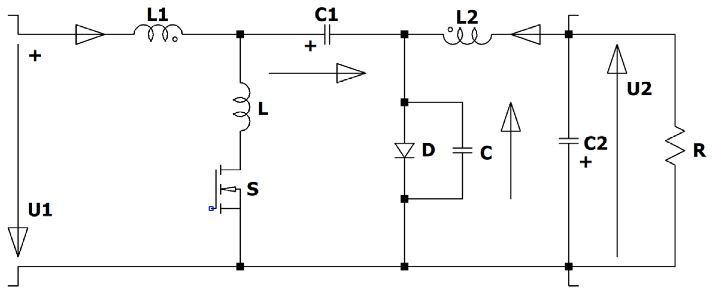
The Zeta converter (Figure 1) has interesting features. The electronic switch is in series with the input source, therefore no inrush current occurs when the converter is connected to a stable voltage source like car-batteries or a DC micro grid. The start-up is achieved by increasing the duty cycle from zero up to the desired value, so no overshot occurs, and the switch can be used as an electronic fuse in case of a short-circuit of the load or in case of no load. The converter has like the Cuk and the Sepic an intermediate capacitor which is charged. The Zeta converter is a fourth order converter consisting of two coils L1, L2, two capacitors C1, C2, an active S and a passive electronic switch D.
First we explain the Zeta converter in the steady state, in the continuous mode and using ideal components (no parasitic resistors, ideal switching). During the on-time of the electronic switch the input voltage is across L1, and the sum of the voltage across C1, the input voltage and the negative output voltage is across L2. The voltage across C1 must be equal to the output voltage. This is obvious when looking at the loop C1, L1, C2 and L2. In the steady state the voltage across an inductor is zero in the mean, therefore the output voltage and the voltage across the intermediate capacitor C1 must be equal. So the voltage across L2 has the same value as the one across L1. When the switch S is turned off, the current of the coils commutates into the diode D. Now the negative voltage across C1 is across L1 and the negative output voltage is at L2. The voltage across L2 looks equal to the one across L1.
Figure 2 shows the voltage across C1, the voltages across the coils, the output and the input voltages, and the control signal of the electronic switch. The voltage across C1 and the output voltage overlap each other and therefore are drawn in different graphs.
Figure 3 shows the voltage stress across the semiconductors. When the transistor is turned on, the voltage across it is zero in the ideal case, and when it is turned off, the sum of the input voltage and the voltage across C1 is blocked by the electronic switch. One can therefore observe that the sum of the input and the output voltages stresses the transistor. The negative sum of the input voltage and the voltage across C1 is blocked by the diode, when the switch is on and zero (because it turns on when the switch turns off), when the switch is off. Both semiconductors must hold the sum of the input and the output voltages (of course increased by a security factor).
The current through the coils increases during the on-time of the switch and decreases during the off-time. It is obvious that the mean current through the output coil L2 is equal to the load current. The load current is nearly constant. The current through the output capacitor corresponds to the current ripple of the output coil L2. During the on-time the capacitor C1 is discharged by the current through L2 and charged during the off- time by the current through L1.
1.2. Influence of the Intermediate Capacitor
In the Figure 2, Figure 3, Figure 4 and Figure 5 the intermediate capacitor is large (330 µF), so the voltage across it is nearly constant. The output voltage is smoothed by the LC filter composed of the coil L2 and the output capacitor C2. A ripple across C1 is therefore permissible. A pulse capacitor can be used instead of an electrolyte capacitor. Figure 6 shows the influence of the value of the intermediate capacitor. The currents through the coils, the load current, the input voltage, the voltage across C1, the output voltage and the control signal of the electronic switch are shown for two capacitor values.
2. ZCS QR Zeta Converter
To achieve zero current switching (ZCS) behavior, two additional components are necessary, an inductor L and a capacitor C. The inductor L is connected in series to the electronic switch S. So the current through it starts with zero, when the switch is turned on. The capacitor is connected in parallel to the diode. This is shown in Figure 7.
2.1. Step by Step Description
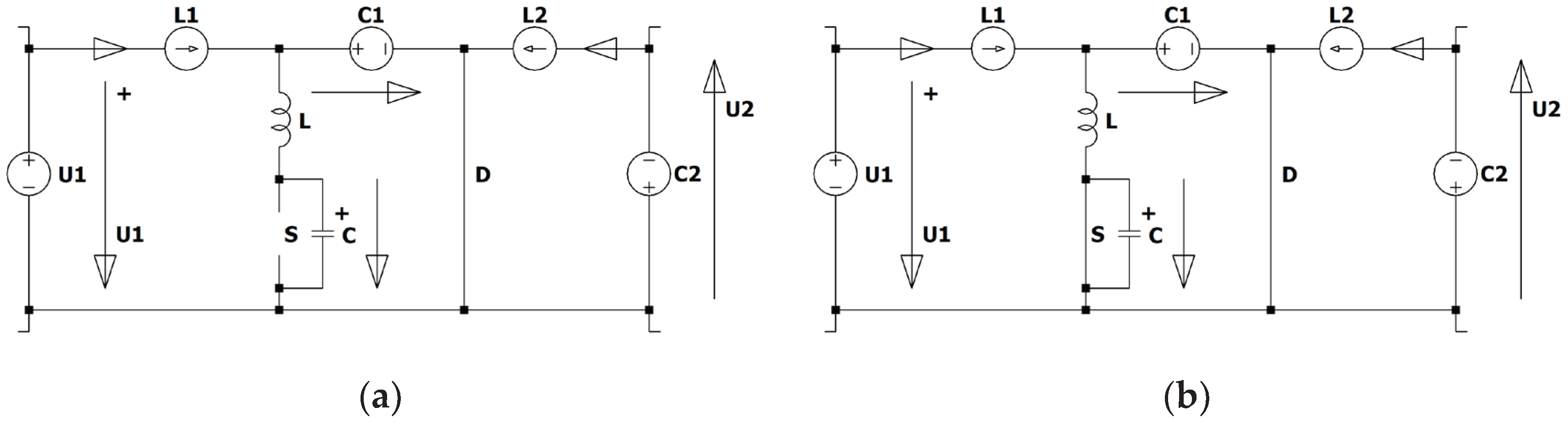
A period of the converter is now analyzed based on the assumptions that the main inductors L1 and L2 are large compared to the resonant inductor L in series to the electronic switch S, and the capacitors C1, C2 are large compared to the resonant capacitor C in parallel to the diode D. The capacitors can now be modelled as voltage sources, and the currents through the coils can be represented by current sources. This is shown in Figure 8.
We start with the free-wheeling mode M0, the diode D is on and the switch S is off. The equivalent circuit is shown in Figure 9.
When the electronic switch S is turned on, mode M1 starts (Figure 10).
The current through the switch S increases and correspondingly the current through the diode D decreases. The voltage across L is the sum of the input voltage U1 and the voltage across C1, which is equal to the output voltage U2. The change of the current can be written by
Integration leads to a linearly rising current
When the current reaches the sum of the currents through the inductors, diode D turns off and mode M2 begins. The equivalent circuit is drawn in Figure 11.
The easiest way to describe this equivalent circuit is by using the state space description. With the help of the Kirchhoff’s laws one gets the state equations, and the initial conditions are the end values of mode M1 according to
Using the matrix description one gets
Laplace transformation leads to
The current through the coil can be calculated by
Solving the determinant leads to the current in the Laplace domain
With the correspondences
one gets
The current through the resonant coil L can now be sketched. During mode M1 the current increases linearly through L until it reaches the sum of both currents through the inductors, and the current through the diode has vanished and the diode D turns off. During M2 the current is described by a sinus function. If the amplitude of the sinus waveform is higher than IL1+IL2, the current can become negative. During the time when the current is negative the active switch S can be turned off. The current commutates into the body diode of the electronic switch, when it is a MOSFET, or into the antiparallel diode, when the switch is e.g. an IGBT. When the current reaches zero and starts to be positive, this diode turns off. Figure 12 sketches the current through the resonant coil.
The necessary condition for ZCS is that the amplitude of the sinusoidal wave must be larger than the sum of the currents through the coils
Keep in mind that the voltages across both capacitors are equal. One can replace UC1 by U2.
The voltage across the resonant capacitor is given by
leading to
The current through L reaches zero within the time interval T2a
The resonant period lasts
and the half period is therefore
The time interval is longer than a one half-period. The rest of the time can now be found by
So one gets
Therefore, the mode M2a (during which the current through L is positive when in the resonant mode) lasts
During Mode M2b the same equation (10) for the current through L is valid. The current is now negative and still flows through the channel of the MOSFET (in case of an IGBT it would flow through the antiparallel diode). The switch can now be turned off with ZVS without switching loss. From Fig. 12 one obtains for the time between the current reaches the sum of IL1 and IL2 until it goes through zero
For the complete duration during which the current is negative we get
With
one can also write
The voltage across the resonant capacitor C in parallel to the diode D is still positive at the end of mode M2. The capacitor C will now be discharged by the sum of both inductor currents. This is mode M3 (see Figure 13). When the capacitor C is discharged, the diode D turns on and the converter is again in mode M0.
The converter can be controlled by a constant on-time and a variable off-time of the active switch S. The operating frequency of the converter is therefore variable and not constant, as it is in a pwm controlled converter.
2.2. u-Zi Diagram
Another way to describe the ZCS QR Zeta converter is with the help of the u-Zi diagram.
Figure 14.
QR Zeta converter: u-Zi diagram..
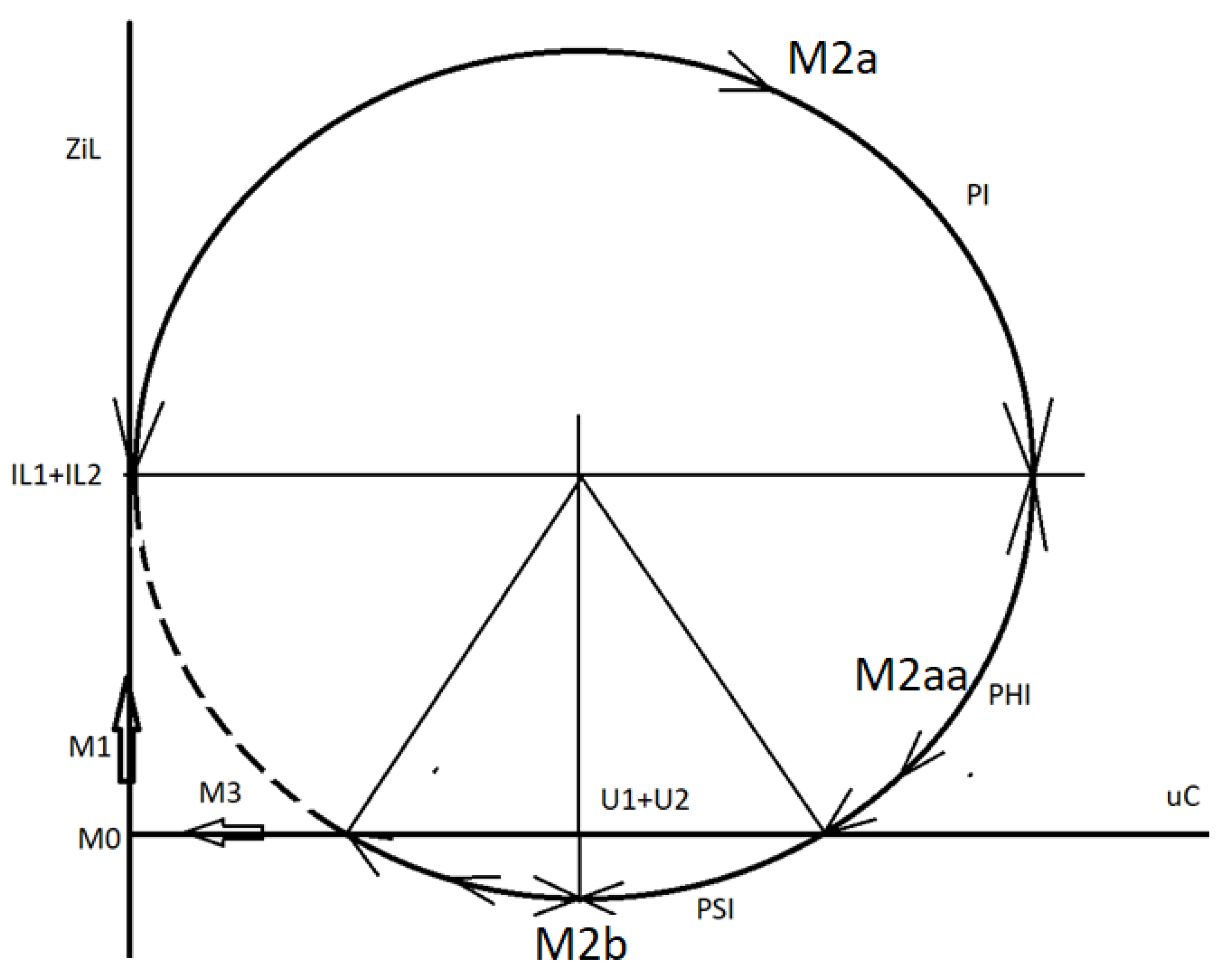
The u-Zi diagram (Fig. 14) has a horizontal axis concerning the voltage across the resonant capacitor and a vertical axis for the product of the resonant impedance and the current through the resonant coil. During M0 the voltage across C is zero, because the diode is conducting and no current is flowing through the resonant coil L. Therefore, mode M0 is described by a point at the origin of the coordinate system. During M1 the current through L increases until it reaches IL1+IL2. During this mode the diode is still conducting, and the voltage across the capacitor is therefore still zero. This mode is a vertical line in the u-Zi diagram. When the ringing starts and M2 begins, the trajectory is a circle in the ideal case. To find the center point, we look at the equivalent circuit of mode M2. A damped ringing can be described by a spiral which ends in the center point. The resonant capacitor is then charged to U1+U2, so there is no voltage across the resonant inductor, and the current through it does not change and no current flows through the capacitor, so the voltage is constant across C. So one gets the center point at [U1+U2, Z(IL1+IL2)]. The full period of the ringing lasts according to (15). The duration of mode M2aa (the current through L is positive) can be found by the angles phi or psi. With
one can calculate the angles according to
The angle of mode M2a is
The duration of M2a and M2b can now be found by a simple rule of proportion
The voltage across the resonant capacitor C at the end of mode M2 can easily be found with the sentence of Pythagoras from the u-Zi diagram according to
The time interval of mode M3 therefore lasts
The duration of mode M1 can be found from (2) according to
2.3. Design
The pwm controlled Zeta converter has a voltage transformation ratio of
and the duty cycle d is given by
The mean value of the current through L2 is equal to the load current. With a current ripple of 3 A per coil the maximum current of the sum of both inductor currents is 22 A. With the ZCS condition
one can write for the characteristic admittance
or for the characteristic impedance, it must be lower than 2.7 Ω
Another way to design the resonant elements is shown in the section concerning the Sepic.
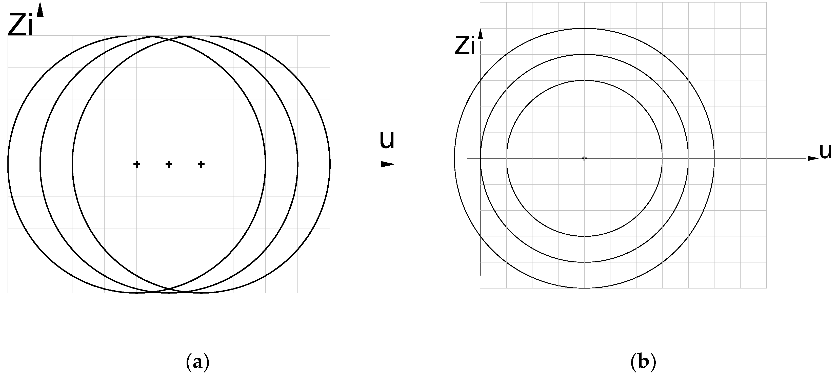
Fig. 15.a shows the circles describing the equivalent circuit of mode M2 for a constant sum of the input and the output voltages for three sums of the currents through the coils of the converter. The center points are marked. The lowest circle is the one which can be used for the ZCS. The second one reaches zero current at one point. This circle is connected with the highest currents through the coils to achieve ZCS. The uppermost circle does not reach the horizontal axis. It should be mentioned that, although ZCS does not occur, the switching losses are reduced and so it can also be useful to operate the converter in this way.
In Fig. 15.b the currents through the coils are taken constant and the sum of the voltages across the input and the output changes. Again the center points are marked. The leftmost circle does not reach the ZCS condition. The middle one touches the voltage axis and the two rightmost one makes ZCS possible. From all these circles one can deduce that the turning off after ¾ of the circle leads to a fixed on-time with some tolerance, when the values of the components change. From Figure 15 it is evident that the converter is only useful for nearly-fixed voltages and currents.
2.4. Simulation
The simulation is done with the parameters U1=24 V U2=36 V IL1=10 A ILoad=6 A, TR=20 µs, so one gets with
for the resonance components C=1.2 µF, L=8.6 µH.
Figure 16 shows the signal diagrams. The signals are: the voltage across the resonant capacitor, the output voltage, the input voltage, the control signal; the current through the resonant inductor, the sum of the currents through the converter coils, and the load current.
Figure 17 shows the trajectory of the current through the resonance coil over the voltage across the resonant capacitor and the u-Zi diagram.
Figure 18 shows the same signals as in Fig. 16, but here the currents through the coils are not constant. They have a current ripple as in a real converter. Fig. 19 shows the same signals as in Figure 18, but with a smaller load resistor (higher load current). Figure 20 shows the trajectory and the u-Zi diagrams.
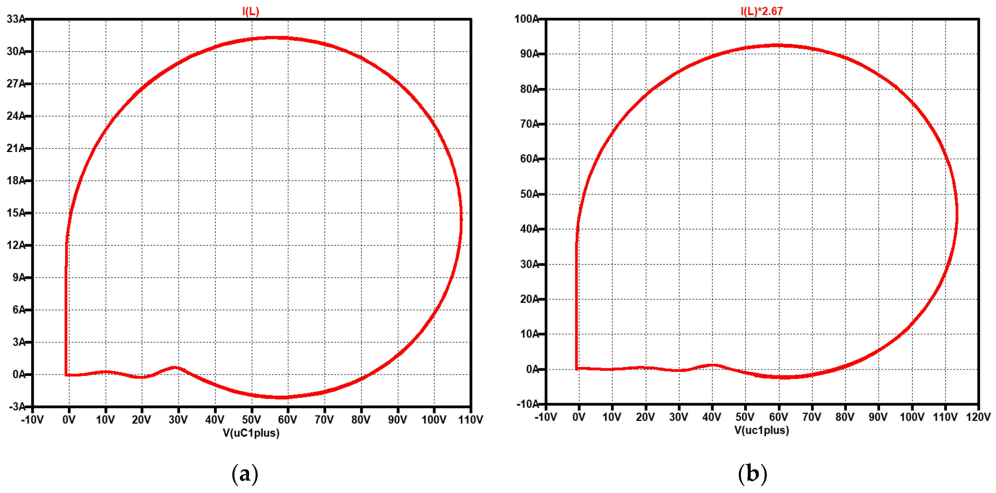
Figure 17.
ZCS QR Zeta, simulation with current and voltage sources: (a) trajectory resonant current over resonant capacitor voltage; (b) uZ-i diagram.
Figure 17.
ZCS QR Zeta, simulation with current and voltage sources: (a) trajectory resonant current over resonant capacitor voltage; (b) uZ-i diagram.
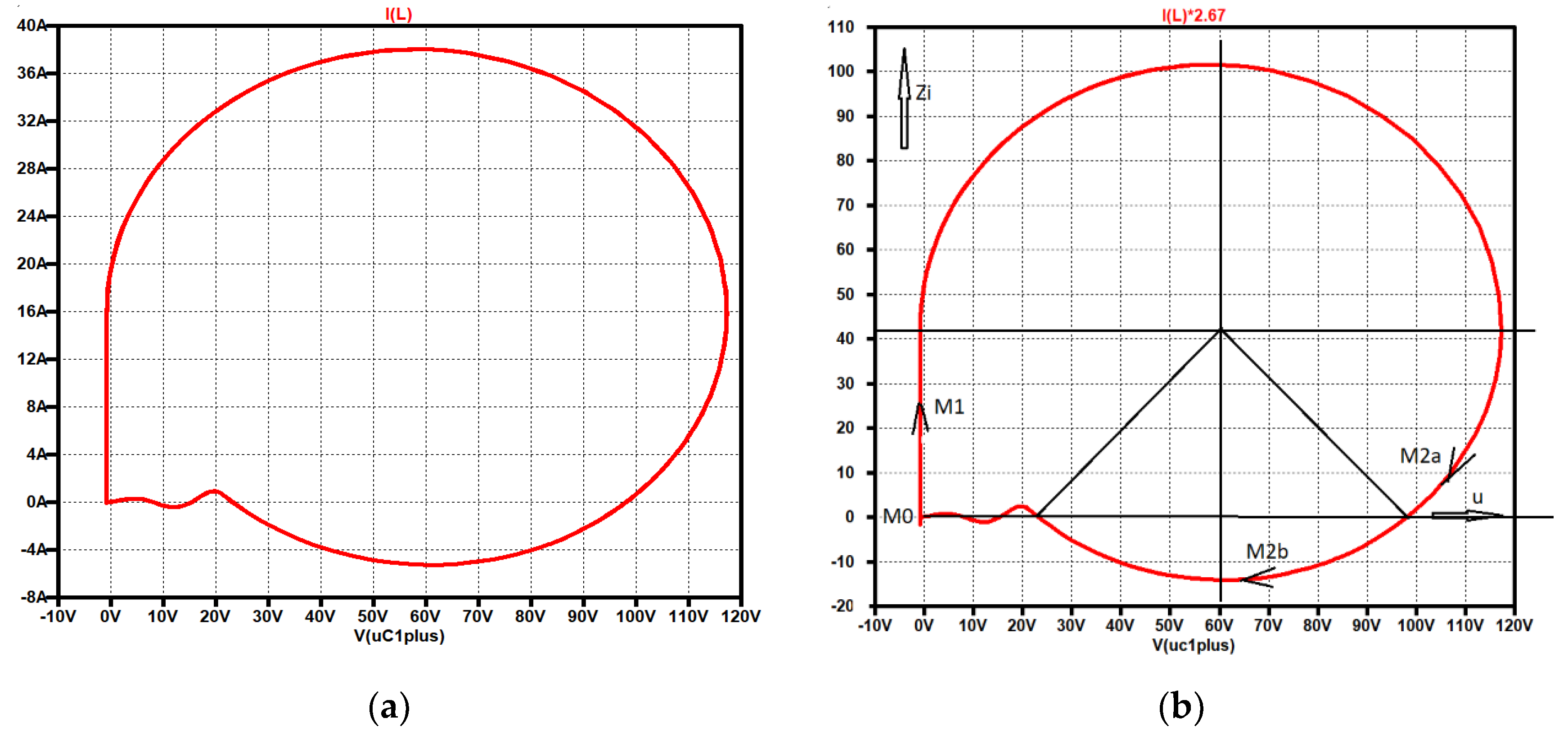
Figure 18.
ZCS QR Zeta, simulation with capacitors and coils: (a) simulation circuit; (b) up to down: voltage across the resonant capacitor (dark green), output voltage (green), input voltage (blue), control signal (turquoise); current through the resonant inductor (red), sum of the currents through the converter coils (dark violet), load current (brown).
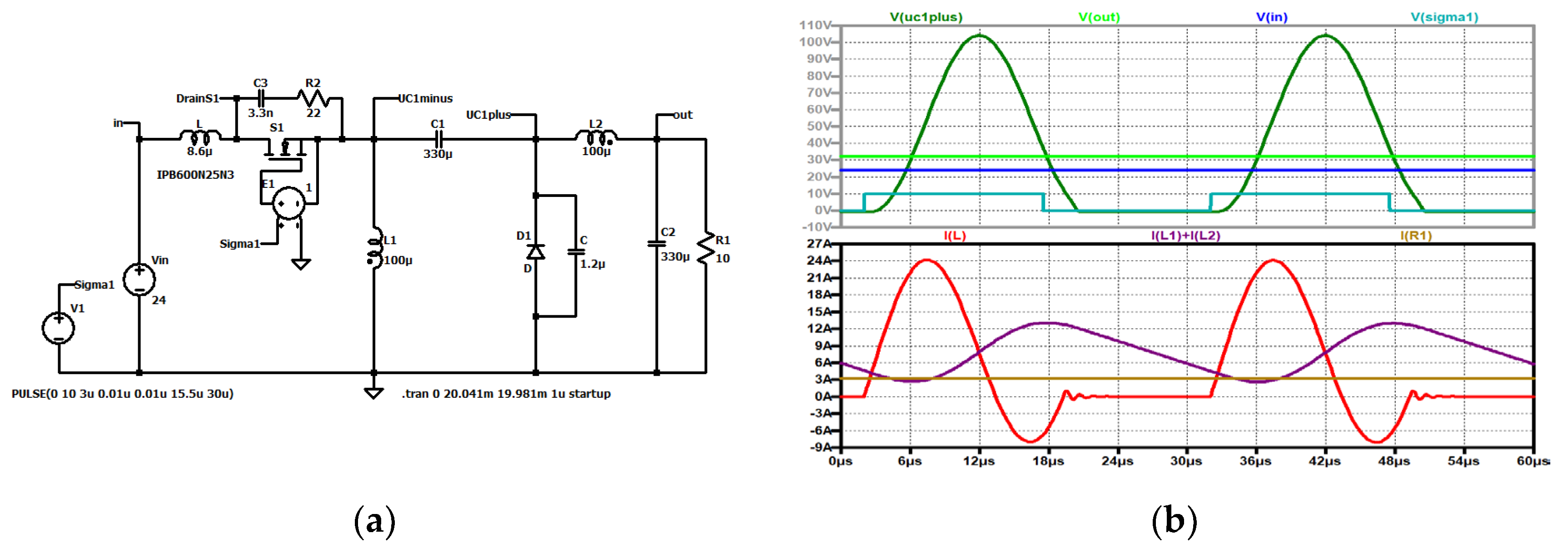
Figure 19.
ZCS QR Zeta, simulation with capacitors and coils: (a) simulation circuit; (b) signals as in Figure 18.
Figure 19.
ZCS QR Zeta, simulation with capacitors and coils: (a) simulation circuit; (b) signals as in Figure 18.
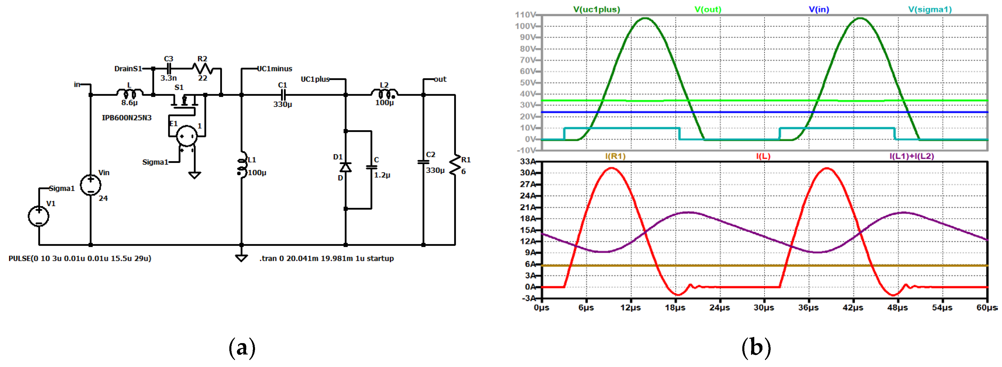
Figure 20.
ZCS QR Zeta, parameters as in Fig. 18: (a) trajectory resonant current over resonant capacitor voltage; (b) uZ-i diagram.
Figure 20.
ZCS QR Zeta, parameters as in Fig. 18: (a) trajectory resonant current over resonant capacitor voltage; (b) uZ-i diagram.
3. ZVS QR Zeta Converter
To achieve ZVS a small capacitor C is connected in parallel to the active switch S, and a small inductor L is connected in series to the electronic switch S. This can be seen in Figure 21.
3.1. Step by Step Description
Again we have several modes which follow each other. The circuit is simplified by replacing the coils by current sources and the capacitors by constant voltage sources. During M0 the active switch is on. Figure 22 shows the equivalent circuit.
When the active switch is turned off, M1 begins. The equivalent circuit is depicted in Figure 23.
The current through the coils charges the capacitor C until the voltage reaches U1+UC1 and the diode D turns on (because the voltage across the diode starts to be positive). The duration of mode M1 can be found from
according to
When the passive switch turns on, mode M2 begins. This is the resonance mode. The equivalent circuit can be found in Figure 24.
With Kirchhoff’s laws one can write the state equations. The initial values of the differential equations are the end values of mode M1. One gets
Combination of state equations into a matrix equation leads to
Laplace transformation is used for solving
The current can now be calculated according to
The voltage across the capacitor in the Laplace domain is given by
With the transformation correspondences (9) one gets
A sketch of the voltage across the resonant capacitor is shown in Figure 25.
The amplitude shows the necessary ZVS condition. The amplitude must be higher than the sum of the input and the output voltages
When the sinusoidal wave reaches zero, the body diode turns on. Now one can turn on the switch again with ZVS and mode M3 starts (the active switch turns on again). When the current through the diode reaches zero, the circuit is again in mode M0. Figure 26 shows the equivalent circuit of mode M3.
3.2. u-Zi Diagram
The easiest way to study the resonance is by using the u-Zi diagram (Figure 27).
The duration of M2 can be found from
according to the angle
The complete circle has an angle of 2π, and the duration for running through this angle is . With the simple rule of proportions, one gets for the duration of M2
One can also calculate
and gets for the angle
which leads for the duration of M2 according to
We can also obtain the maximum voltage across the transistor from the u-Zi diagram according to
the maximum current
and the zero voltage condition
The resonance mode determines the off-time of the converter within one period. Fig. 28.a shows the circles describing mode M2 for constant currents through the coils and a variable sum of the input and the output voltages. The left circle leads to ZVS, the second one is the border circle which reaches zero voltage at one point and the right one reaches only low voltage across the switch, but it can be useful to use even this because the switching loss are reduced. Fig. 28.b depicts the circles for a fixed sum of the input and the output voltages for three sum of currents. The higher the current the better ZVS is achieved. The middle circle is the one of the border for achieving ZVS. Again it is obvious that the converter is useful for voltages and currents which only change little. The control of the converter is done by constant off-times and variable frequency.
Figure 28.
ZVS QR Zeta circles describing mode M2: (a) constant current, variable voltage; (b) constant voltage, variable current.
Figure 28.
ZVS QR Zeta circles describing mode M2: (a) constant current, variable voltage; (b) constant voltage, variable current.
3.3. Simulation
4. Other Fourth Order Converters
Apart from the Zeta converter, other fourth order converters are used, especially the Sepic and the Cuk converters. All these topologies have an intermediate capacitor which separates the input and the output sides of the converters. The Sepic converter is frequently used in the automotive industry, and the Cuk converter can be found in solar and also in aerospace applications. Compared to the Zeta converter, both these converters have the advantage of using low side switches, and the disadvantage of a large inrush current, when applied to a stable DC input voltage.
4.1. ZCS QR SEPIC
The circuit diagram of the Sepic converter is shown in Figure 31 and the modification into a ZCS QR converter in Figure 32. Once again a small inductor L in series to the electronic switch and a capacitor in parallel to the diode D are necessary.
4.1.1. Modes of the Converter
For the analyzes we replace the capacitors C1 and C2 by voltage sources and the inductors L1 and L2 by current sources. Now the operation of the converter can be easily described. The equivalent circuit is depicted in Figure 33.
The function of the converter is equal to that of the Zeta converter. Starting from the free-wheeling mode M0, where the transistor is off and the currents through the coils L1 and L2 free-wheel through the diode, the analysis is done. During this mode the currents through the coils decrease, but for the explanation they are considered as constant. The current through the resonant inductor L and the voltage across the resonant capacitor C are zero. The equivalent circuit is shown in Figure 34.
When the transistor is turned on at the beginning of mode M1, the current through the diode D decreases and commutates into the transistor S. The change of the current is influenced (limited) by the resonant inductor L. When the current through the diode reaches zero, the currents through the current sources (which represent the coils of the converter) now flow through the switch and the diode turns off. The equivalent circuit of mode M1 is shown in Figure 35.
Now mode M2, the resonance, starts. The equivalent circuit is shown in Figure 36. The capacitor C in parallel to the diode and the inductor L in series to the switch S form a resonant circuit. When the current through the resonance inductor reaches zero, the transistor can be turned off. Now the current can flow through the diode which is in parallel to the electronic switch. In case of a MOSFET this is the body diode of the transistor, or in case of an IGBT a parallel connected diode. The turn-off of the transistor happens with no voltage across the switch and therefore no switching loss occurs. The transistor must be turned off during the time, when the current through the resonant coil L is negative. When the transistor is turned off during this time interval, the parallel diode turns off when the current through L starts to be positive again. Now during the last mode M3 (Figure 37), the capacitor C in parallel to the diode gets discharged and when the voltage reaches zero, the diode D turns on and the converter is again in mode M0. The control of the converter is done by the length of the free-wheeling mode. The turn-on phase is nearly constant.
4.1.2. u-Zi Diagram
The easiest way to illustrate the concept is by using the u-Zi diagram (Figure 38).
During mode M0 no current is flowing through the resonant coil L and the resonant capacitor is short-circuited by the diode. So M0 is in the origin of the coordinates. During M1 the current increases through the resonance inductor till it reaches the sum of both inductor currents. M1 is therefore a vertical line. When the diode turns off, the resonant capacitor C and the resonant coil L now form a resonant circuit which constitutes a circle in the u-Zi diagram. From Figure 36 one realizes that when this circuit makes a damped ringing, the trajectory will end, so that all currents will flow through the coil L and the capacitor will be charged to the sum of the input U1and the output U2 voltages. This is the center point of the circle. The current through L is positive during M2a and negative during M2b. During M2b the switch must be turned off. When the current through L reaches zero again, M3 starts and the capacitor C is discharged. When the voltage across it reaches zero, the diode D turns on and the converter is again in mode M0.
Figure 39 shows circles of mode M2 for different currents and voltages. Again it is obvious that the QR concept is only useful for converters with relatively small tolerances of the input and output ranges.
The duration of mode M2a (where the current is positive) can now be easily determined. The angle linked to M2a is
The complete circle has an angle of 2π and the time for one period is given by (c.f.).
The duration of mode M2a is therefore
In the same way one can calculate the duration of M2b according to
The duration of M1 and M3 must be taken directly from the equations describing these modes and are equal to the ones (31, 32) one get for the Zeta converter.
From the diagram we can also directly obtain the ZCS condition according to
the maximum voltage across the switch
and the maximum current through the switch
4.1.3. Design
We start with the derivation of the current through the transistor. In the same way the current is decreasing through the diode. The velocity of the change of the current through the diode influences the reverse recovery behavior to a large amount. During M1 the sum of the input and the output voltages is across L. (Remark: it is easier to say “the output voltage” instead of “the voltage across C1” as they have the same value and for the design the output voltage is the important parameter.) For a desired rise time of the current one gets the value of the resonant inductor according to
When one turns off the transistor after ¾ of the resonance period and chooses this period, one can estimate the necessary value of the resonant capacitor according to
Example: TM1=1 µs, T=10 µs, maximum sum of the current 15 A, U1=24 V, U2=36 A leads to
4.1.4. Simulation
The signals shown in Figure 41 are: the voltage across the resonant capacitor, the current through the resonant coil, the current through the converter coils, the output voltage, the input voltage, and the control signal of the active switch. On the right side the u-Zi diagram is depicted.
4.2. ZVS QR SEPIC
A small change of the position of the resonance capacitor leads to a ZVS converter. The capacitor is now placed in parallel to the switch. The circuit diagram is displayed in Figure 42 and the equivalent circuit in Figure 43.
4.2.1. Explanation
For the description of the circuit the capacitors and the coils of the original converter are replaced by voltage and current sources (Figure 43). The inductors have in practice a typical ripple of about 20 %, but in reality the capacitor voltages are nearly constant. The description starts from the driving stage. The transistor is on, and the voltages across the converter coils L1 and L2 are positive and the currents through them increase. Figure 44 shows the equivalent circuit of this mode which we call M0.
Mode M1 starts, when the transistor is turned off. The equivalent circuit is shown in Figure 45. The current commutates into the resonance capacitor C and the voltage across it rises linearly. The currents through the coils are constant, so the inductor L has no influence in this mode and is therefore not shown in the circuit diagram.
When the voltage reaches the sum of the voltage across C1 (which is equal to the input voltage) and the output voltage, the diode D turns on, mode M1 ends and mode M2 starts. M2 is depicted in Figure 46.
A resonance between L and C occurs, and when the voltage across C changes its direction the diode in parallel to the active switch turns on. Now one can turn on the switch again. This must be done before the current through L becomes positive again.
During M3 (Figure 47) the current through the switch (and the inductor L) rises until the complete currents through L1 and L2 flow through the switch, and the circuit is again in mode M0.
4.2.2. Design
The capacitor is chosen in such a way that the rise time of the voltage across the transistor is TM1=0.5 µs. The input and output voltages are equal to the values used in section 3.3. The elements can be calculated by (41) and (50). Figure 49 shows the simulation circuit and Figure 50 the results.
The results are depicted in Figure 50.
4.3. ZCS QR CUK
According to the concept to construct a ZCS QR Cuk, an inductor L must be connected in series with the active switch, and a capacitor C has to be connected in parallel to the passive switch. The input voltage is U1 and the output voltage is U2. The converter inverts the input voltage.
Figure 51.
ZCS QR CUK: circuit diagram.
The function is equal to the other converters described before. The description starts with mode M0 (the free-wheeling, Figure 52.a). When the transistor is turned on, mode M1 starts (Figure 52.b) and ends, when the current through the diode gets zero and the diode turns off. Now the circuit is in the resonance mode M2 (Figure 53.a). During mode M3 (Figure 53.b) the resonant capacitor is discharged completely, the diode turns on and the circuit is again in the free-wheeling mode M0 (Figure 52.a).
Figure 54.a shows the circuit of the simulation. The capacitors and the coils are replaced by constant sources. The voltage across the resonant capacitor and the current through the resonant inductor are shown (Figure 54.b). The design and the u-Zi diagram are equal to the other ZCS QR converters described in this paper.
4.4. ZVS QR CUK
According to the concept to construct a Zero Voltage Switching Quasi Resonant Converter, a capacitor C has to be connected in parallel to the active switch and an inductor L must be connected in series with the active switch. The input voltage is U1 and the output voltage is U2. The circuit diagram is shown in Figure 55.
The function is explained with the equivalent circuits which follow each other during a switching period. The transistor is on during mode M0 (Figure 56.a). When the transistor is turned off, mode M1 starts and the current commutates into the capacitor (Figure 56.b). When the diode turns on, mode M2 and the resonance begin (Figure 57.a). During M3 (Figure 57.b) the current through L increases till it reaches the sum of the currents through the two coils L1, L2 and the diode turns off. The converter is now again in mode M0 (Figure 56.a). The design and the u-Zi diagram are equal to the other ZVS QR converters described in this paper.
5. Conclusions
The quasi resonant concept uses a resonant circuit to influence the rise and fall times of the voltage across or the current through the switch of a converter. The switching event of the active switch happens, when the current through or the voltage across it is zero. So no switching loss occurs. In this paper the Zeta converter is studied in detail and the two other usually used fourth order converters, the Sepic and the Cuk, are also treated. The function is very similar. Besides studying the modes of the converters with mathematical equations, the graphical u-Zi diagram can be used. From this diagram one can easily obtain the durations of the modes and the current and the voltage stress. The u-Zi diagram helps to properly design the resonant devices. The concept is effective, when the voltage and the current ranges at the input and the output sides are limited. The active switches used in power converters have been improved during the last years by new technologies like GaN or SiC, which enable higher voltages, larger currents and faster switching. The fast switching reduces the switching losses but increases electromagnetic interference (EMI). With the QR concept the EMI can be reduced. The ZVS concept has the additional advantage that no current, caused by the discharge of the output capacitor of the active switch, occurs (which happens at the ZCS concept). It should be remarked that because of the resonant wave the forward losses are increased. The voltage stress is higher than in an pwm converter. Interesting further investigations are the combination of QR converters with the tristate concept [22], coupling both converter coils magnetically (integrated magnetics) and the interruption of the resonance to enlarge mode M2. The paper can be useful as a lecture note.
Funding
This research received no external funding.
Data Availability Statement
The data are included in the paper.
Acknowledgments
The author thanks Dr. Karl Edelmoser for drawing the figures Figures 15, 28, 39, 48.
Conflicts of Interest
The author declares no conflicts of interest.
References
- Liu, K.-H.; Lee, F. C. Y. Zero-voltage switching technique in DC/DC converters. IEEE Transactions on Power Electronics, vol. 5, no. 3, pp. 293-304, July 1990. [CrossRef]
- Liu, K.-H.; F. C. Lee, K.-H. Resonant Switches - A Unified Approach to Improve Performances of Switching Converters. INTELEC ‘84 - International Telecommunications Energy Conference, New Orleans, LA, USA, 1984, pp. 344-351. [CrossRef]
- Maksimovic, D., Cuk, S. A general approach to synthesis and analysis of quasi-resonant converters. 20th Annual IEEE Power Electronics Specialists Conference, Milwaukee, WI, USA, 1989, pp. 713-727 vol.2. [CrossRef]
- Liu, K.-H.; Oruganti, R.; Lee, F. C. Y. Quasi-Resonant Converters-Topologies and Characteristics. IEEE Transactions on Power Electronics, vol. PE-2, no. 1, pp. 62-71, Jan. 1987. [CrossRef]
- Martín, C. D.; Durán Aranda, E.; Litrán, S. P.; Semião, J. Quasi-Resonant DC-DC Converter Single-Switch for Single-Input Bipolar-Output Applications. IECON 2022 – 48th Annual Conference of the IEEE Industrial Electronics Society, Brussels, Belgium, 2022, pp. 1-6. [CrossRef]
- Hasanisadi, M.; Tarzamni, H.; Tahami, F. Comprehensive Reliability Assessment of Buck Quasi-Resonant Converter. 2022 IEEE 20th International Power Electronics and Motion Control Conference (PEMC), Brasov, Romania, 2022, pp. 614-620. [CrossRef]
- Spirov, D. S.; Komitov, N. G. Design of induction motor drive with parallel quasi-resonant converter. 2017 XXVI International Scientific Conference Electronics (ET), Sozopol, Bulgaria, 2017, pp. 1-4. [CrossRef]
- Wen, D.; Chen, Y.; Zhang, B.; Qiu, D.; Xie, F.; Jiang, Z. Transient Analysis of Quasi-Resonant Converter Based on Equivalent Small Parameter Method Considering Different Time Scale. 2019 22nd International Conference on Electrical Machines and Systems (ICEMS), Harbin, China, 2019, pp. 1-5. [CrossRef]
- Barakat, S.; Mesbahi, A.; N’Hili, B.; Et-Torabi, K. ZVS QR boost converter with variable input voltage and load. 2023 3rd International Conference on Innovative Research in Applied Science, Engineering and Technology (IRASET), Mohammedia, Morocco, 2023, pp. 1-6. [CrossRef]
- Hinov, N. Model-Based Design of a Buck ZVS Quasi-Resonant DC-DC Converter. International Conference on High Technology for Sustainable Development (HiTech), Sofia, Bulgaria, 2022, pp. 1-6. [CrossRef]
- Abkenar, P. P.; Marzoughi, A.; Vaez-Zadeh, S.; Iman-Eini, H.; Samimi, M. H.; Rodriguez, J. A Novel Boost-Based Quasi Resonant DC-DC Converter with Low Component Count for Stand-Alone PV Applications. IECON 2021 – 47th Annual Conference of the IEEE Industrial Electronics Society, Toronto, ON, Canada, 2021, pp. 1-6. [CrossRef]
- Allioua, A.; Krause, D.; Zingariello, A.; Griepentrog, G. Reduction of DC/DC Converters EMI Emission Using Bi- and Unidirectional QR-ZVS Topologies. 2023 IEEE 10th Workshop on Wide Bandgap Power Devices & Applications (WiPDA), Charlotte, NC, USA, 2023, pp. 1-6. [CrossRef]
- Allioua, A.; Griepentrog, G. Power and Signal Dual Modulation with QR-ZVS DC/DC Converters using GaN-HEMTs. 2024 IEEE Applied Power Electronics Conference and Exposition (APEC), Long Beach, CA, USA, 2024, pp. 2164-2171. [CrossRef]
- Sooksatra, S. Subsingha, W. Analysis of Quasi-resonant ZCS Boost Converter using State-plane Diagram. 2020 8th International Electrical Engineering Congress (iEECON), Chiang Mai, Thailand, 2020, pp. 1-4. [CrossRef]
- Zhou, Q. and Sooksatra, S. Analysis of Constant Switching Frequency Quasi-Resonant ZVS-ZCS Boost Converter using State-Plane Diagram. 2024 12th International Electrical Engineering Congress (iEECON), Pattaya, Thailand, 2024, pp. 1-6. [CrossRef]
- Lin, T.-J.; Tseng, Y. -S.; Shih, C. -C.; Chen, C. -J. Analysis and Efficiency Improvement of Quasi-Resonant Flyback Converter with Adaptive Valley Detection and Variable Frequency Control. 2024 13th International Conference on Renewable Energy Research and Applications (ICRERA), Nagasaki, Japan, 2024, pp. 1342-1348. [CrossRef]
- Khodabandeh, M.; Afshari; E.; Amirabadi, M. A Family of Ćuk, Zeta, and SEPIC Based Soft-Switching DC–DC Converters. IEEE Transactions on Power Electronics, vol. 34, no. 10, pp. 9503-9519, Oct. 2019. [CrossRef]
- Himmelstoss F.A. Quasi Resonant Zero Current Switching Modified Boost Converter (QRZCSMBC). WSEAS Transactions on Circuits and Systems, Volume 22, 2023, pp. 55-62, E-ISSN: 2224-266X. [CrossRef]
- Mohan, N.; Undeland, T.; Robbins, W. Power Electronics, Converters, Applications and Design. W. P. John Wiley & Sons: New York, NY, USA, 2002.
- Rozanov, Y.; Ryvkin, S.; Chaplygin, E.; Voronin, P. Power Electronics Basics. CRC Press: Boca Raton, FL, USA, 2020.
- Zach, F. Leistungselektronik. 6th ed.; Springer: Frankfurt, Germany, 2022. (In German).
- Himmelstoss, F.A. Reduced Loss Tristate Converters. MDPI Electronics 2025, 14, 1305. [Google Scholar] [CrossRef]
Figure 1.
Circuit diagram of the Zeta converter.
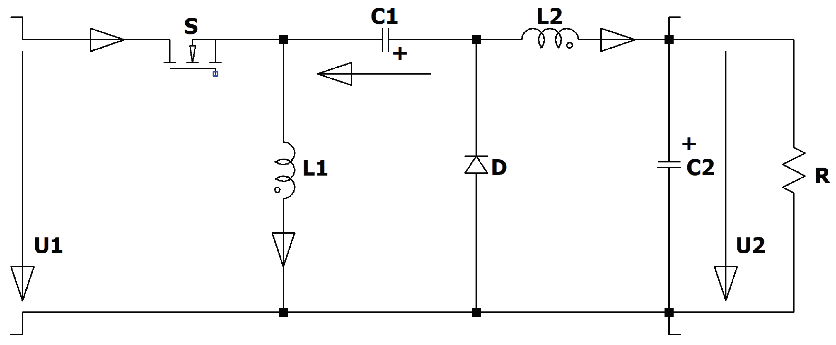
Figure 2.
Zeta converter: (a) simulation circuit; (b) up to down: voltage across the intermediate capacitor C1 (dark green), voltage across L2 (black); voltage across L1 (dark blue); output voltage (green), input voltage (blue), control signal (turquoise)..
Figure 2.
Zeta converter: (a) simulation circuit; (b) up to down: voltage across the intermediate capacitor C1 (dark green), voltage across L2 (black); voltage across L1 (dark blue); output voltage (green), input voltage (blue), control signal (turquoise)..
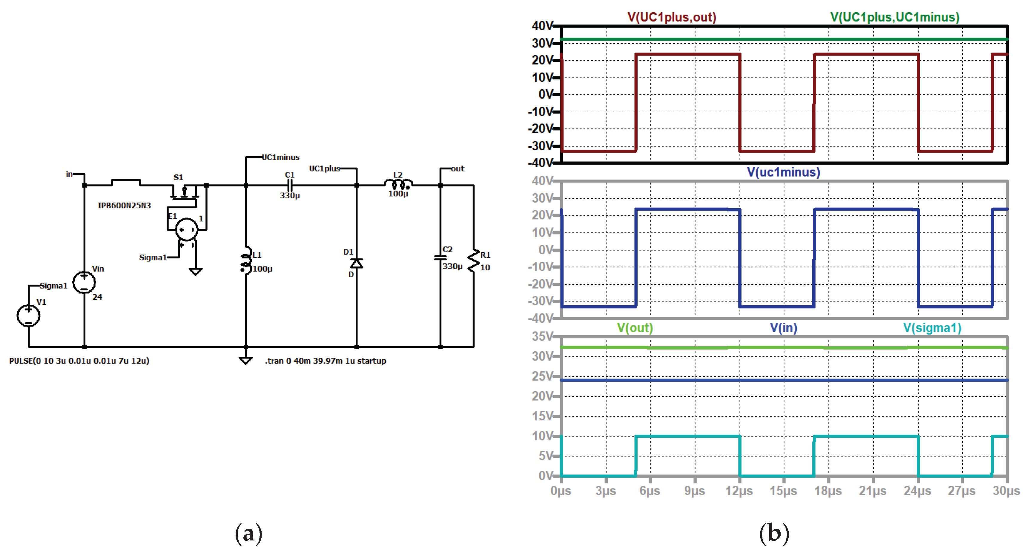
Figure 3.
Zeta converter: (a) simulation circuit; (b) up to down: voltage across the diode (black); voltage across the electronic switch (dark blue); output voltage (green), input voltage (blue), control signal (turquoise).
Figure 3.
Zeta converter: (a) simulation circuit; (b) up to down: voltage across the diode (black); voltage across the electronic switch (dark blue); output voltage (green), input voltage (blue), control signal (turquoise).
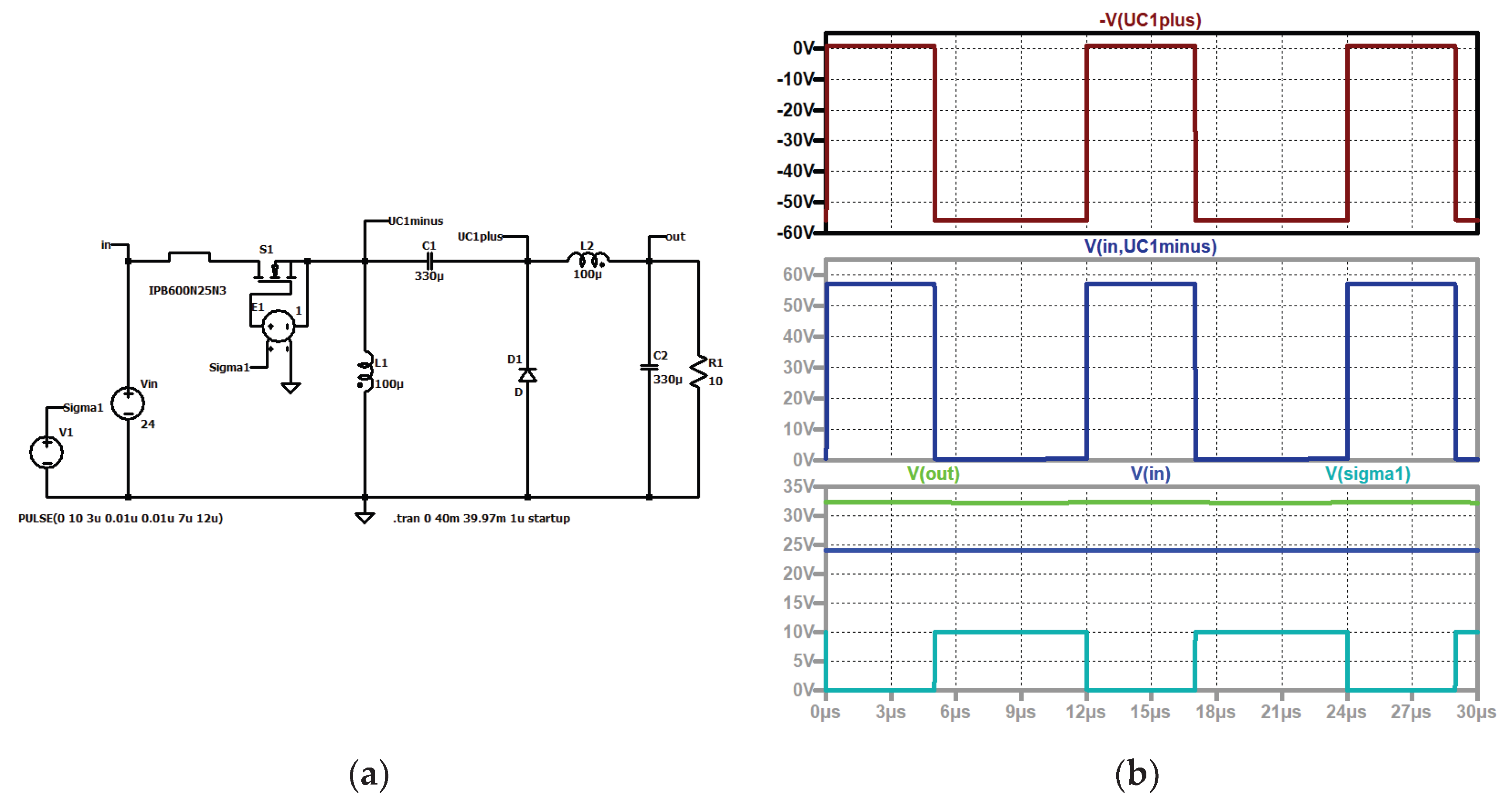
Figure 4.
Zeta converter: (a) simulation circuit; (b) up to down: current through the intermediate capacitor C1 (dark violet), current through the output capacitor C2 (grey); current through L1 (red), current through L2 (violet), load current (brown); output voltage (green), input voltage (blue), control signal (turquoise).
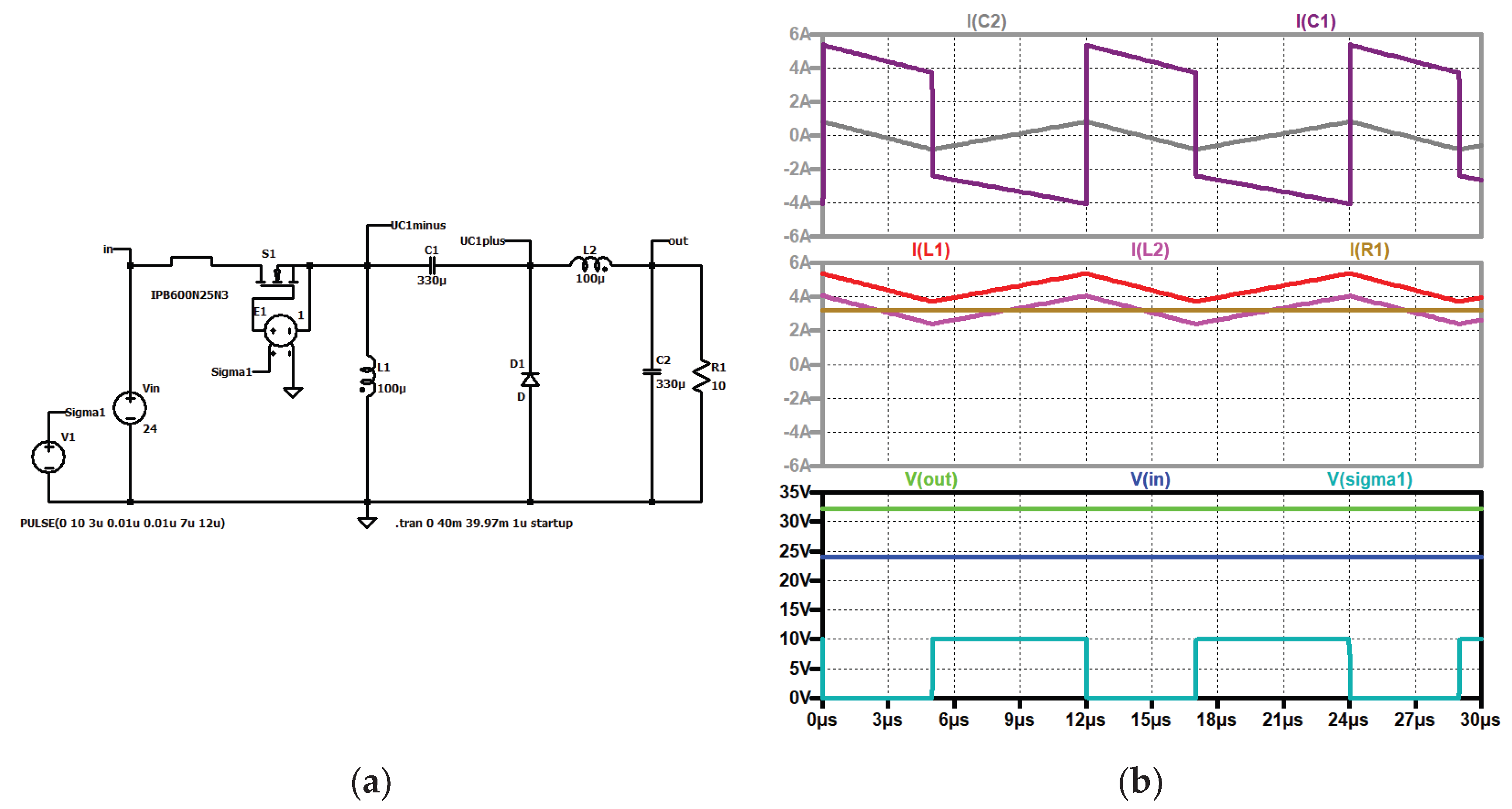
Figure 5.
Zeta converter: (a) simulation circuit; (b) up to down: current through the diode (violet), current through the electronic switch (red); output voltage (green), input voltage (blue), control signal (turquoise).
Figure 5.
Zeta converter: (a) simulation circuit; (b) up to down: current through the diode (violet), current through the electronic switch (red); output voltage (green), input voltage (blue), control signal (turquoise).
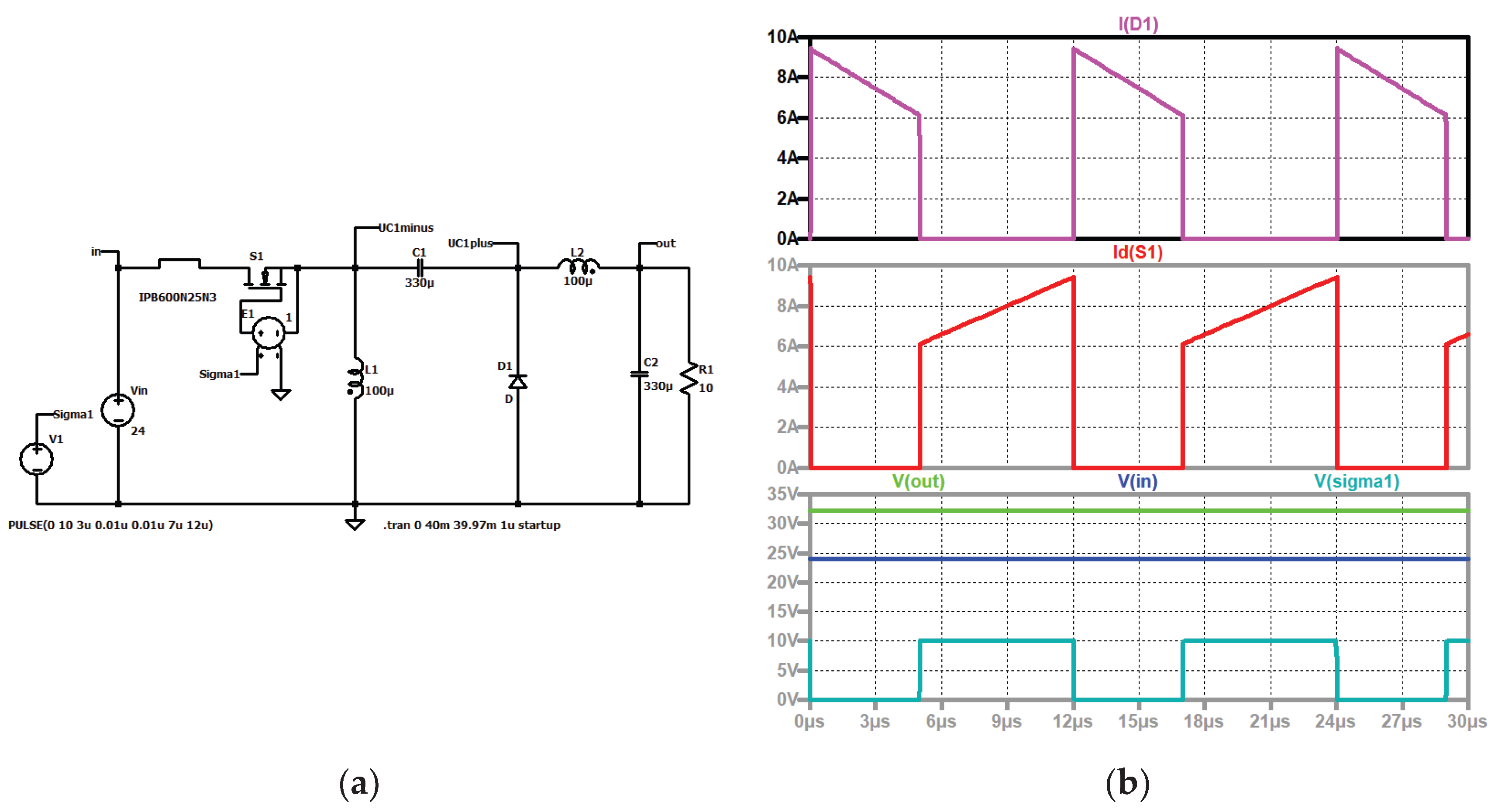
Figure 6.
Zeta converter: up to down: current through L1 (red), current through L2 (violet), load current (brown); output voltage (green), voltage across C1 (grey); input voltage (blue), control signal (turquoise), (a) large capacitor 33 µF; (b) small capacitor 3.3 µF.
Figure 6.
Zeta converter: up to down: current through L1 (red), current through L2 (violet), load current (brown); output voltage (green), voltage across C1 (grey); input voltage (blue), control signal (turquoise), (a) large capacitor 33 µF; (b) small capacitor 3.3 µF.
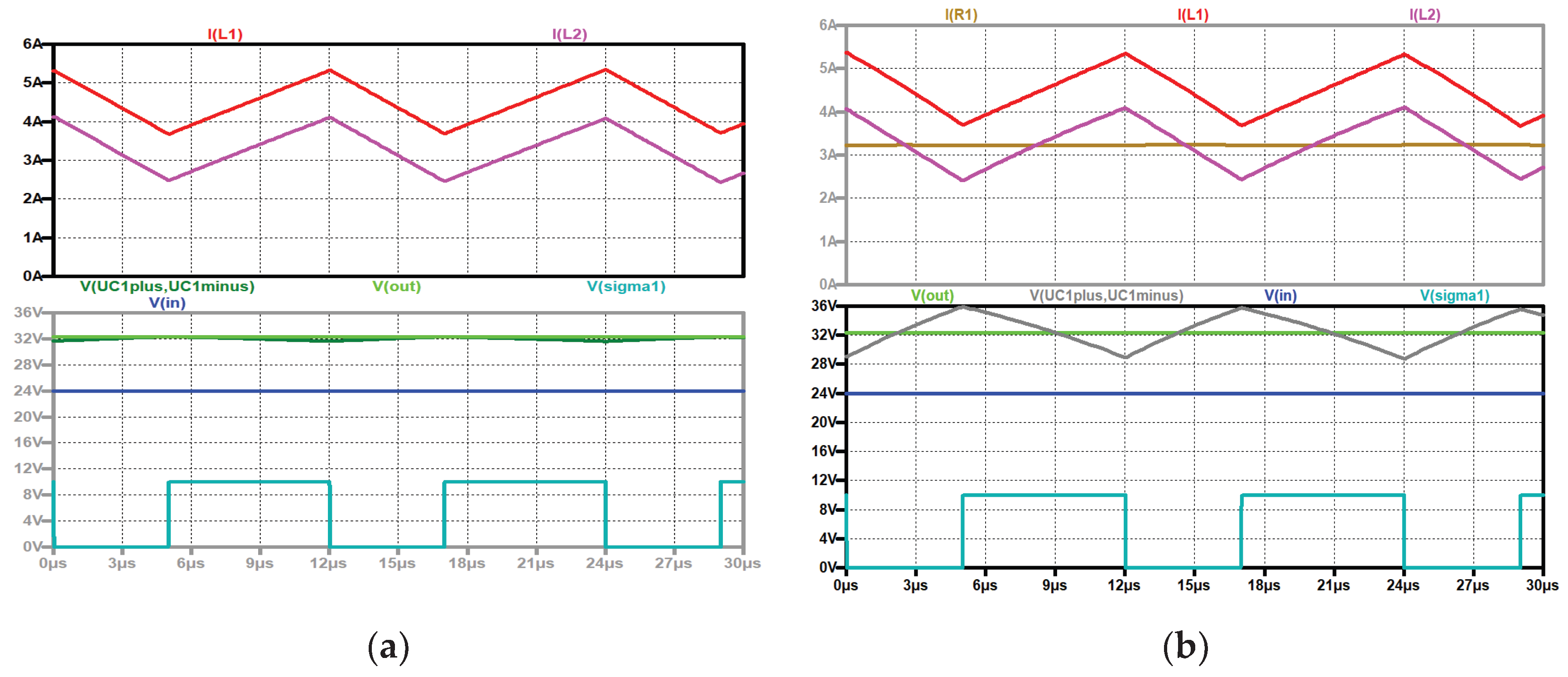
Figure 7.
ZCS QR Zeta converter.
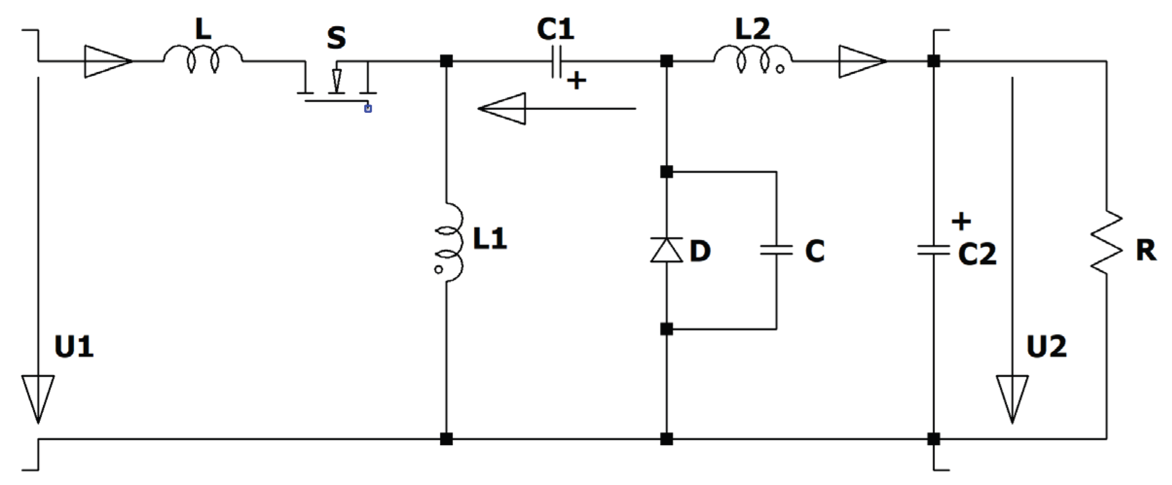
Figure 8.
Reduced (simplified) ZCS QR Zeta converter.
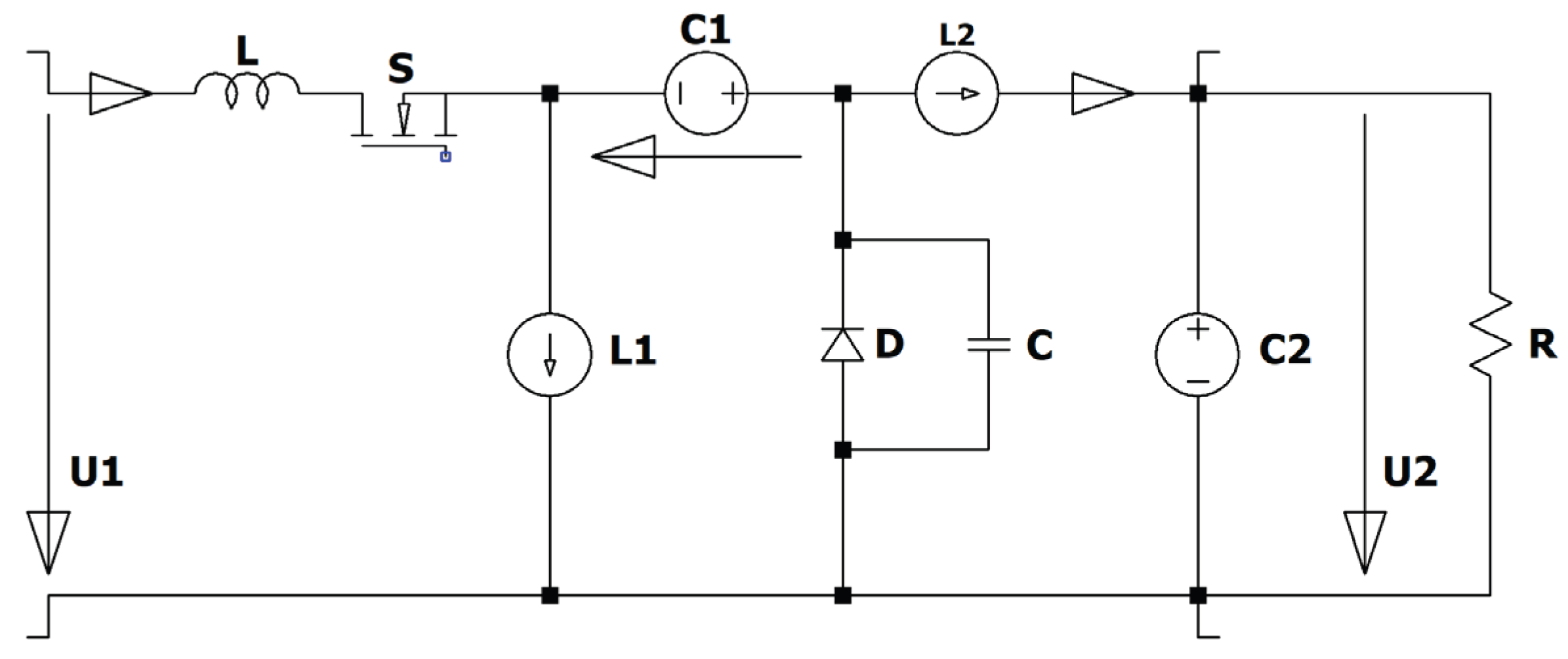
Figure 9.
Equivalent circuit M0 (freewheeling).

Figure 10.
Equivalent circuit M1 (switch is turned on).
Figure 11.
Equivalent circuit M2 (resonance).
Figure 12.
Current through the resonant coil L.
Figure 13.
Equivalent circuit M3 (discharge C).
Figure 15.
ZCS QR Zeta, circles describing mode M2: (a) constant voltage, variable current; (b) constant current, variable voltage.
Figure 15.
ZCS QR Zeta, circles describing mode M2: (a) constant voltage, variable current; (b) constant current, variable voltage.
Figure 16.
ZCS QR Zeta, simulation with current and voltage sources: (a) simulation circuit; (b) up to down: voltage across the resonant capacitor (dark green), output voltage (green), input voltage (blue), control signal (turquoise); current through the resonant inductor (red), sum of the currents through the converter coils (dark violet), load current (brown).
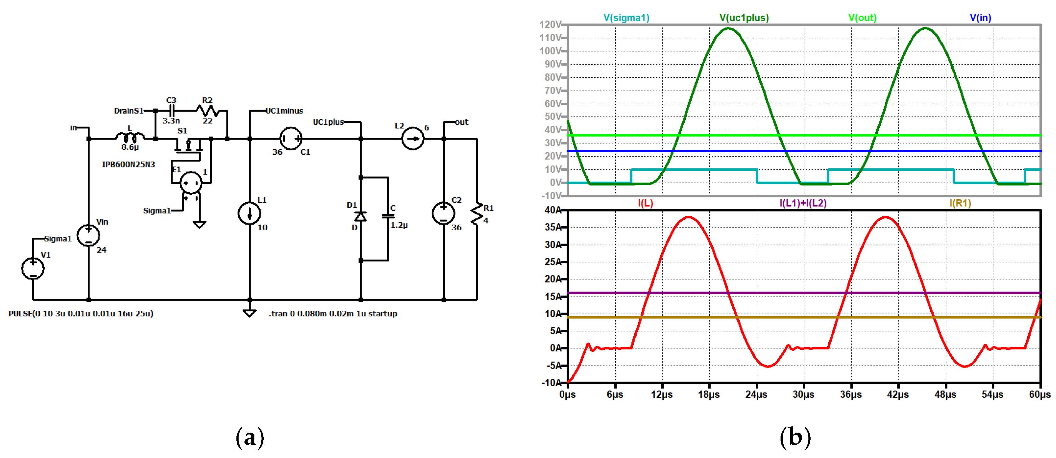
Figure 21.
Circuit diagram of the ZVS QR Zeta converter.
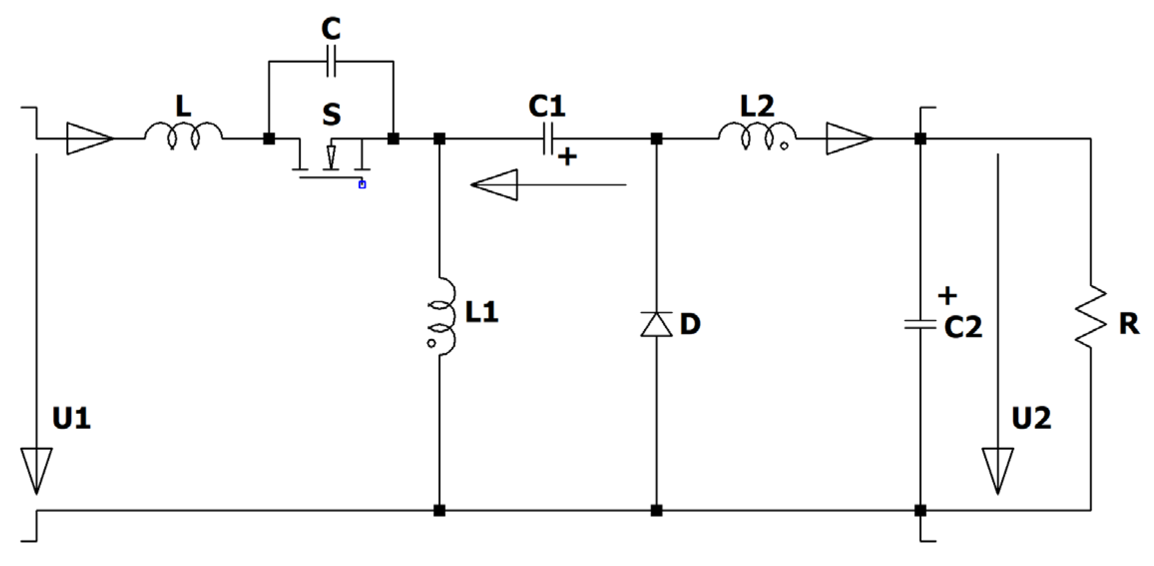
Figure 22.
ZVS QR Zeta converter: mode M0, the switch is on.
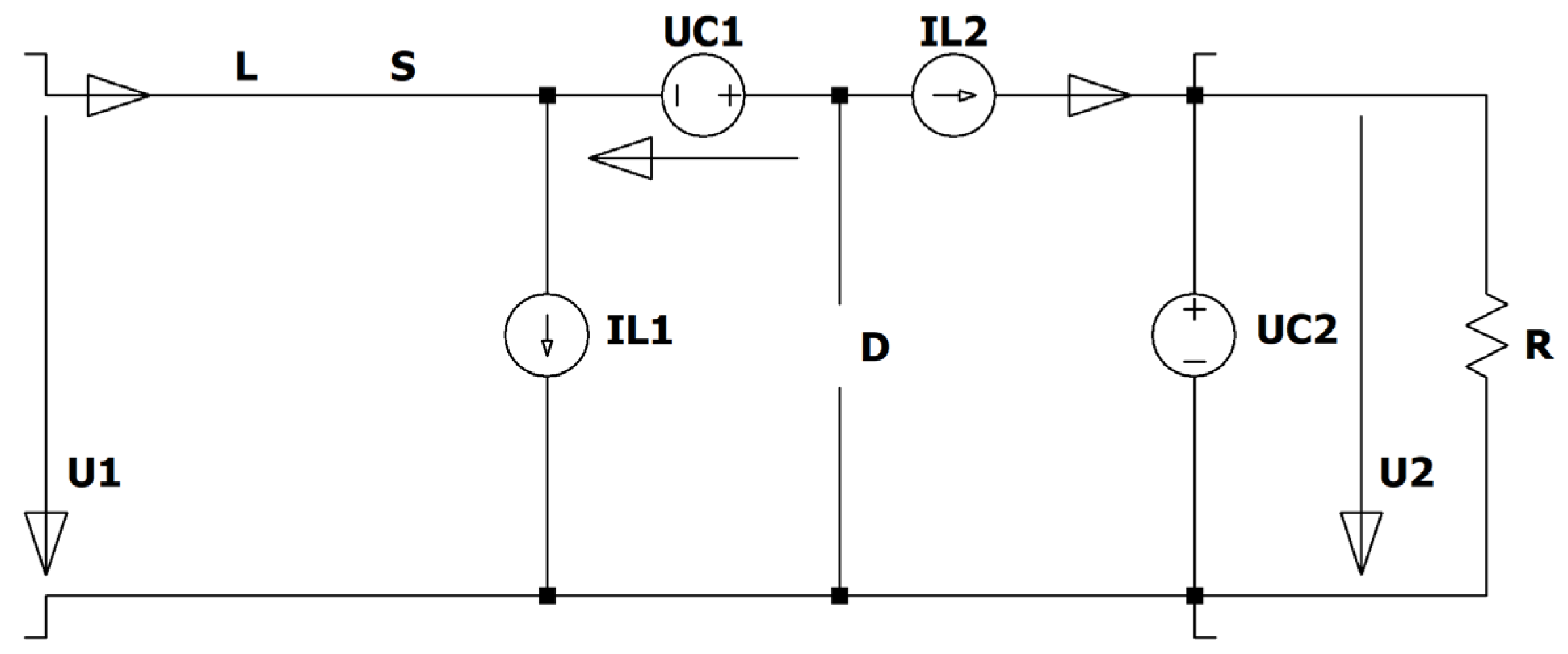
Figure 23.
ZVS QR Zeta converter: mode M2, the switch is turned off, the resonant capacitor is charged.
Figure 23.
ZVS QR Zeta converter: mode M2, the switch is turned off, the resonant capacitor is charged.
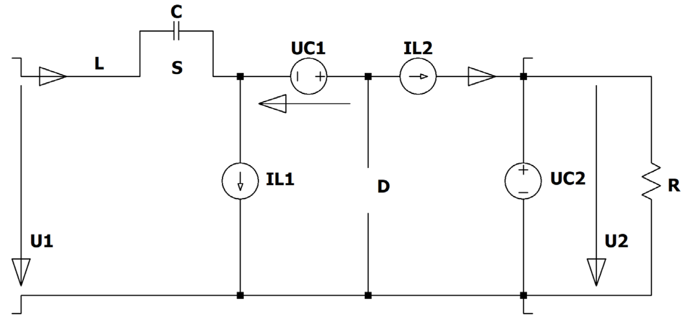
Figure 24.
ZVS QR Zeta converter: mode M2, the resonance.
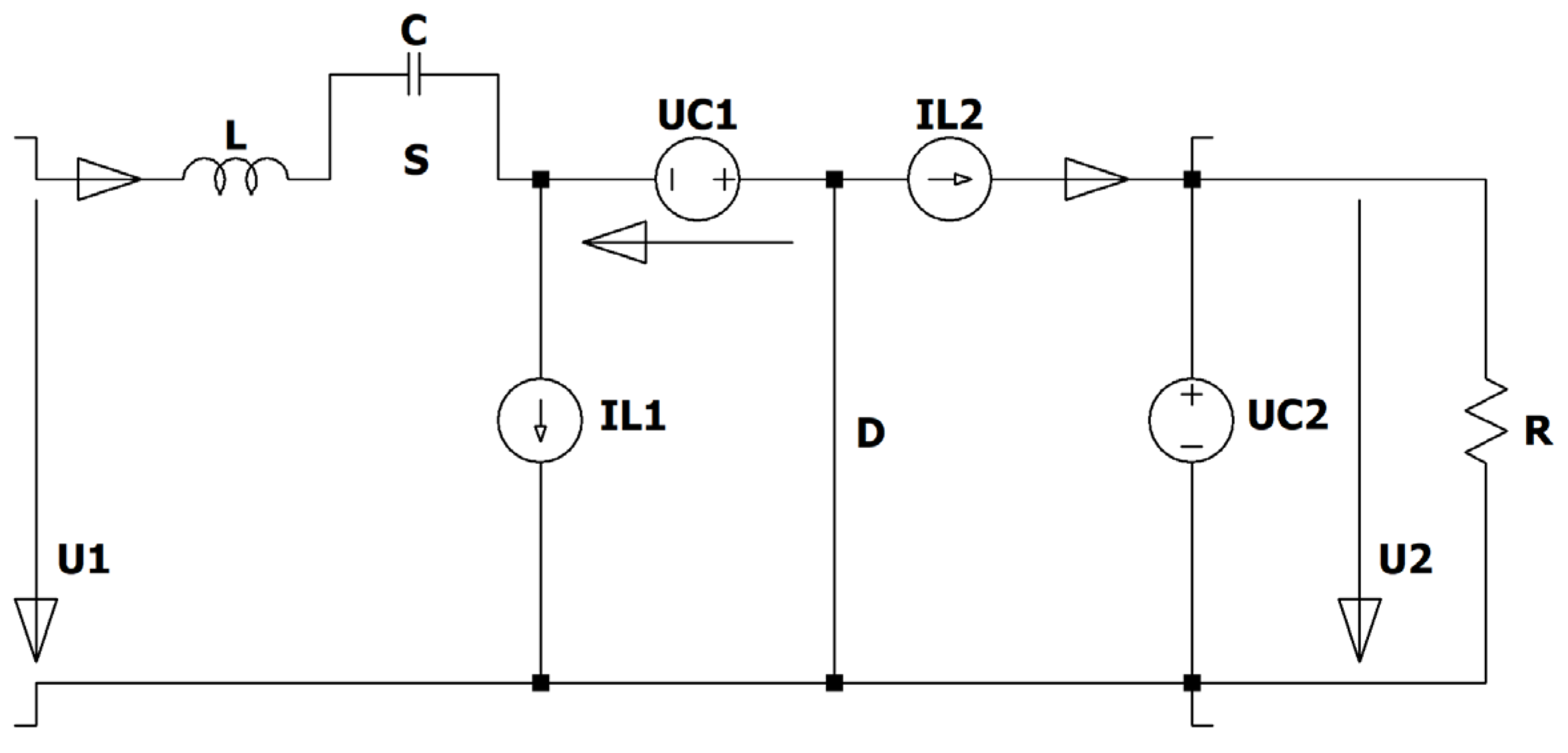
Figure 25.
ZVS QR ZETA converter, voltage across the resonant capacitor.
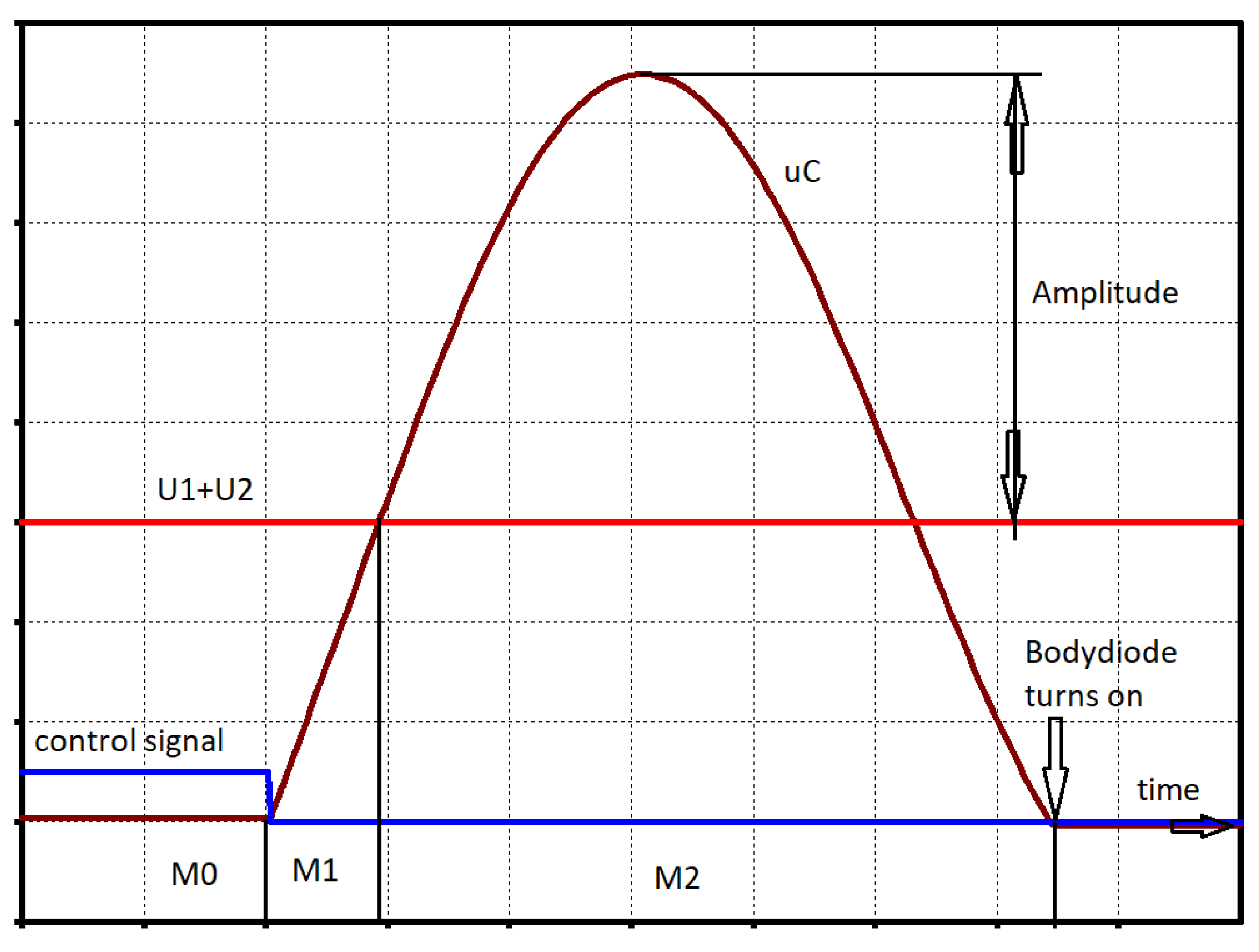
Figure 26.
ZVS QR Zeta converter, mode M3, the current commutates from the diode to the switch.
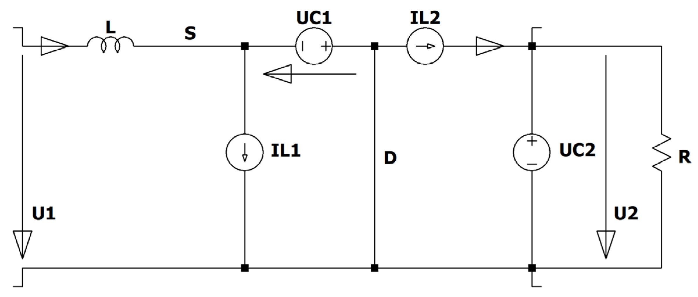
Figure 27.
ZVS QR Zeta converter, u-Zi diagram.
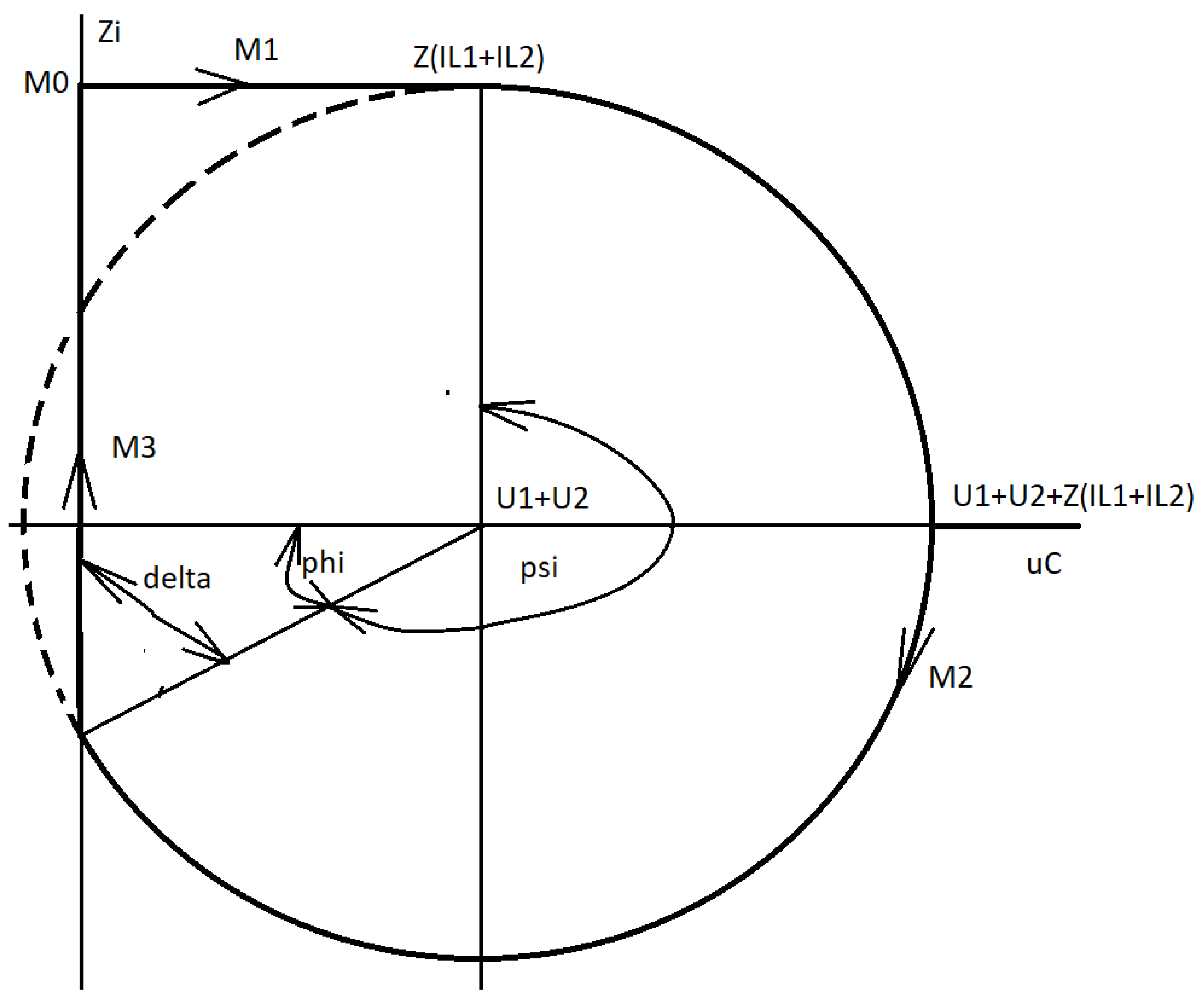
Figure 29.
ZVS QR Zeta: simulation circuit.
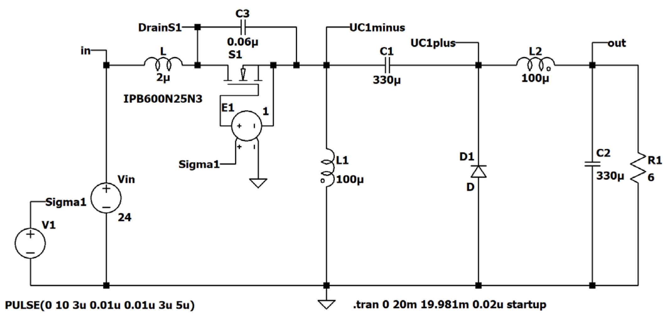
Figure 30.
ZVS QR Zeta: (a) voltage across the resonance capacitor (green), current through the resonance coil (red); (b) trajectory.
Figure 30.
ZVS QR Zeta: (a) voltage across the resonance capacitor (green), current through the resonance coil (red); (b) trajectory.
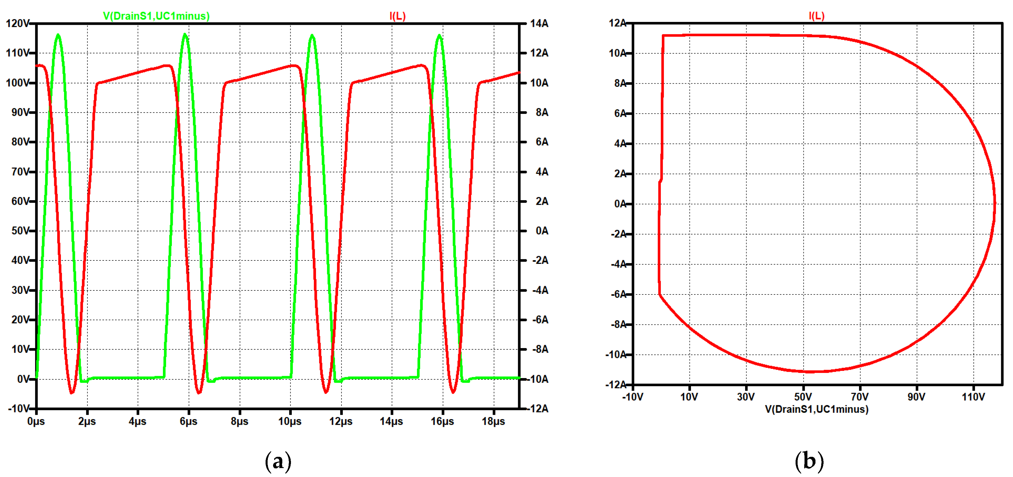
Figure 31.
Circuit diagram of the SEPIC converter.
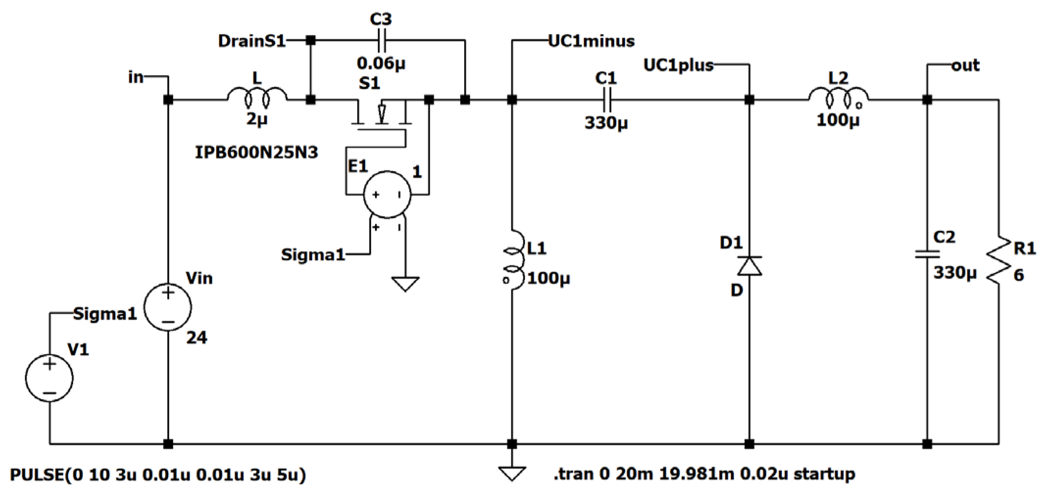
Figure 32.
Circuit diagram of the ZCS QR SEPIC converter.
Figure 33.
ZCS QR SEPIC: equivalent circuit.
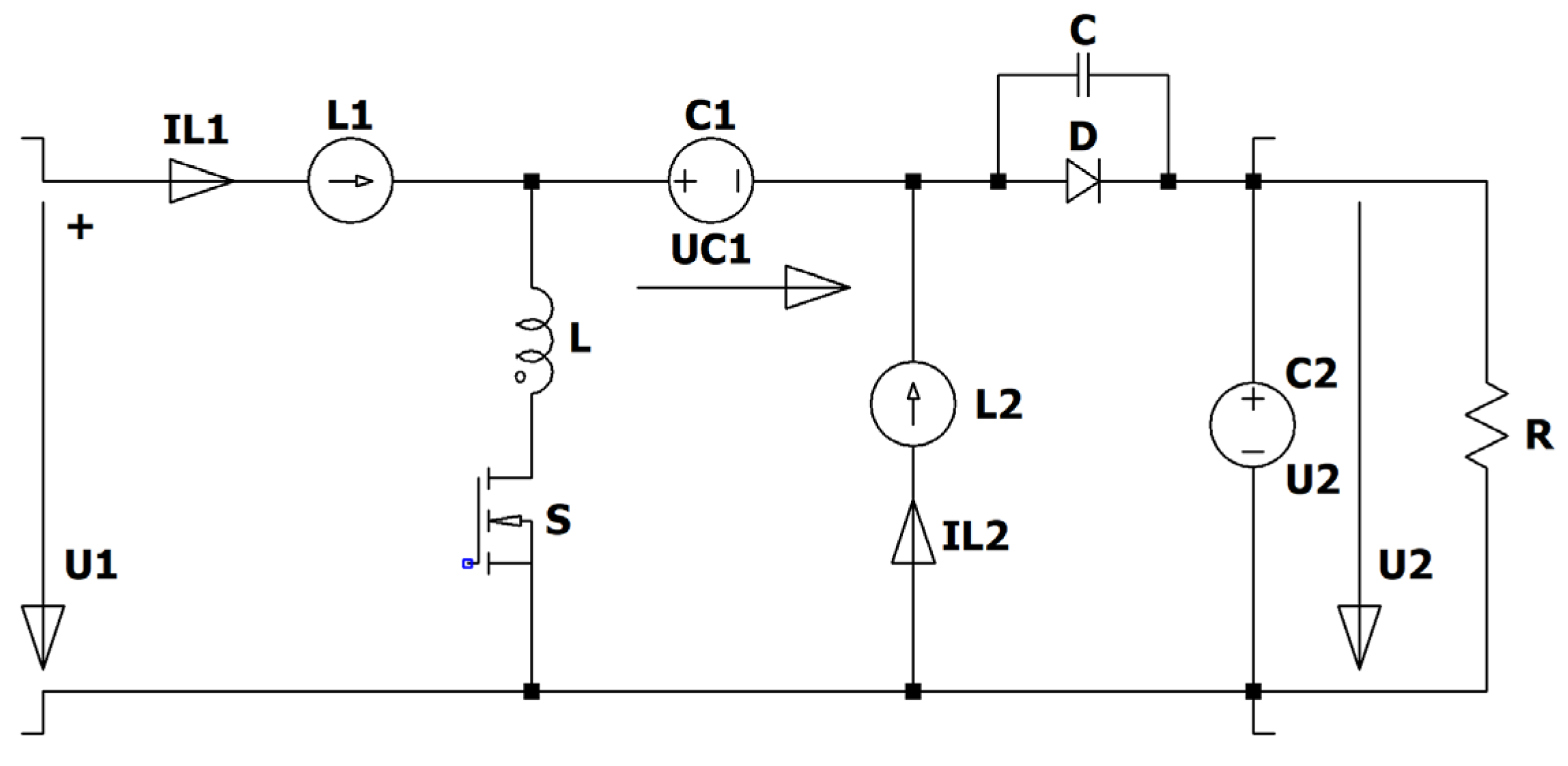
Figure 34.
ZCS QR SEPIC: mode M0.

Figure 35.
ZCS QR SEPIC: mode M1.
Figure 36.
ZCS QR SEPIC: mode M2.
Figure 37.
ZCS QR SEPIC: mode M3.
Figure 38.
ZCS QR SEPIC: u-Zi diagram.
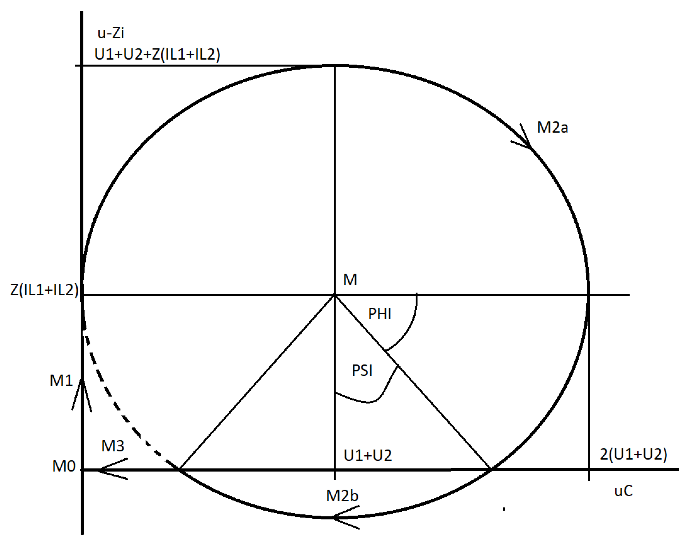
Figure 39.
ZCS QR SEPIC circles describing mode M2: different currents and voltages are shown.
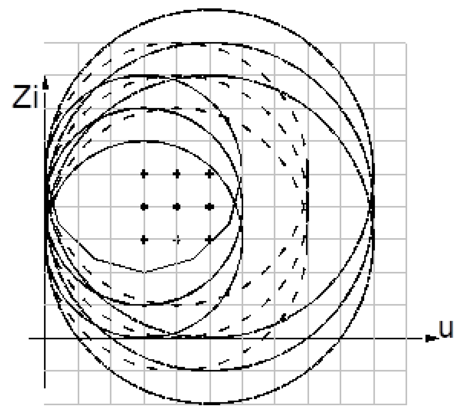
Figure 40.
ZCS QR Sepic: simulation circuit.
Figure 41.
ZCS QR SEPIC: (a) up to down: voltage across the resonant capacitor (dark green); current through the resonant coil (red), sum of the currents through the converter coils (violet); output voltage (green), input voltage (blue), control signal (turquoise); (b) u-Zi diagram.
Figure 41.
ZCS QR SEPIC: (a) up to down: voltage across the resonant capacitor (dark green); current through the resonant coil (red), sum of the currents through the converter coils (violet); output voltage (green), input voltage (blue), control signal (turquoise); (b) u-Zi diagram.
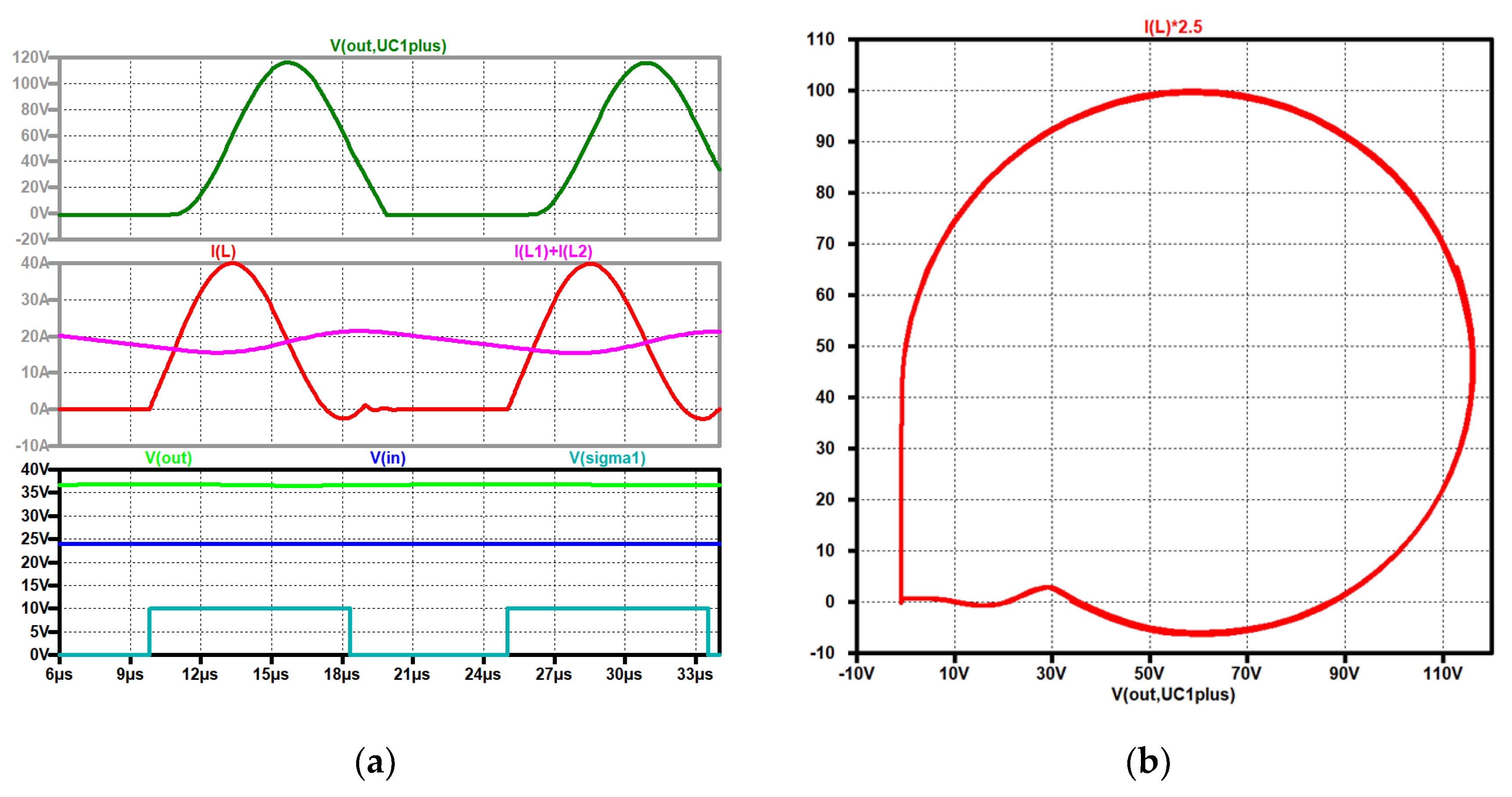
Figure 42.
Circuit diagram of the ZVS QR SEPIC.
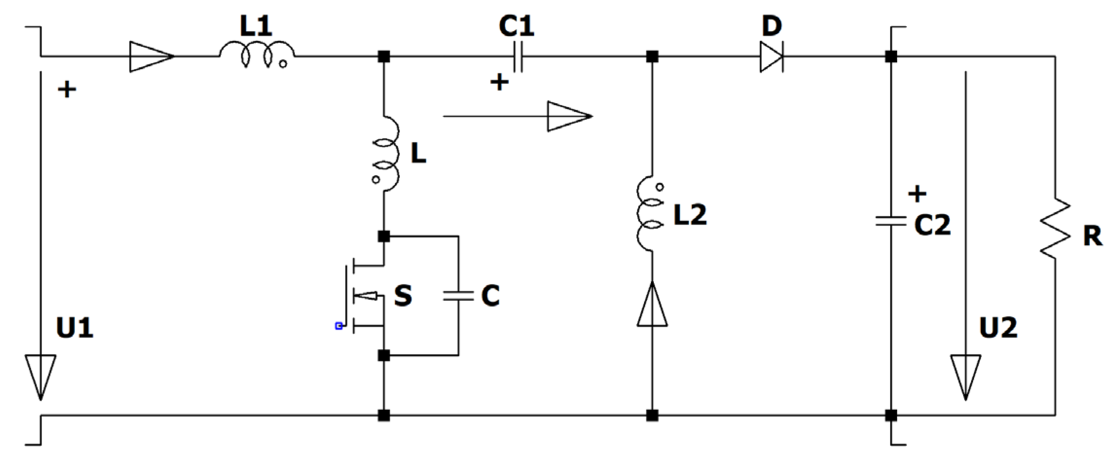
Figure 43.
ZVS QR SEPIC: equivalent circuit.
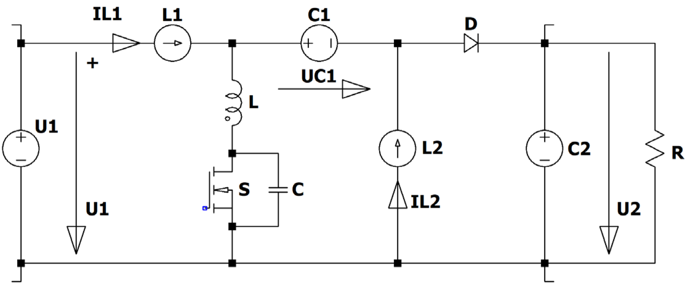
Figure 44.
ZVS QR SEPIC: M0.
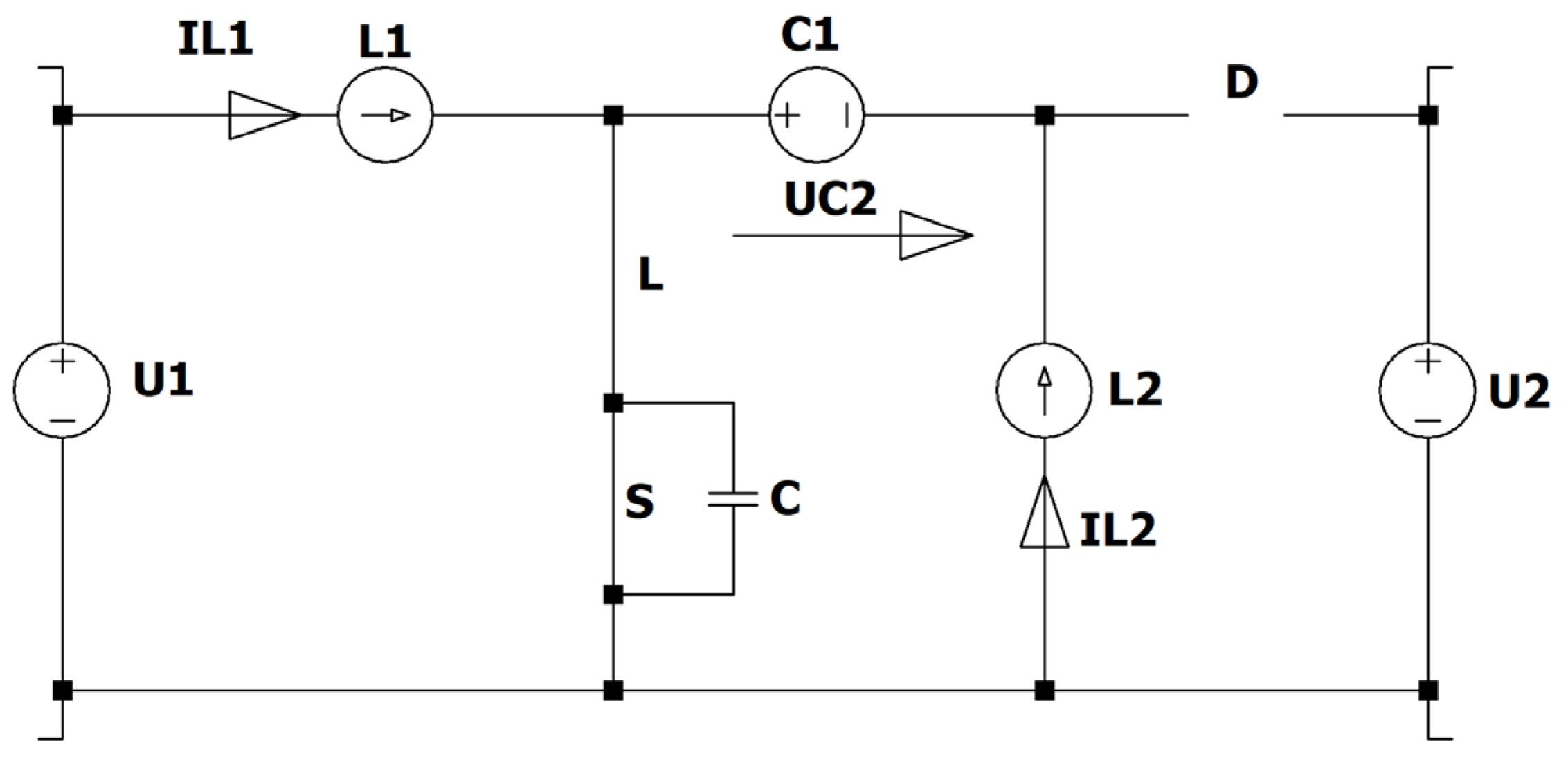
Figure 45.
ZVS QR SEPIC: M1.
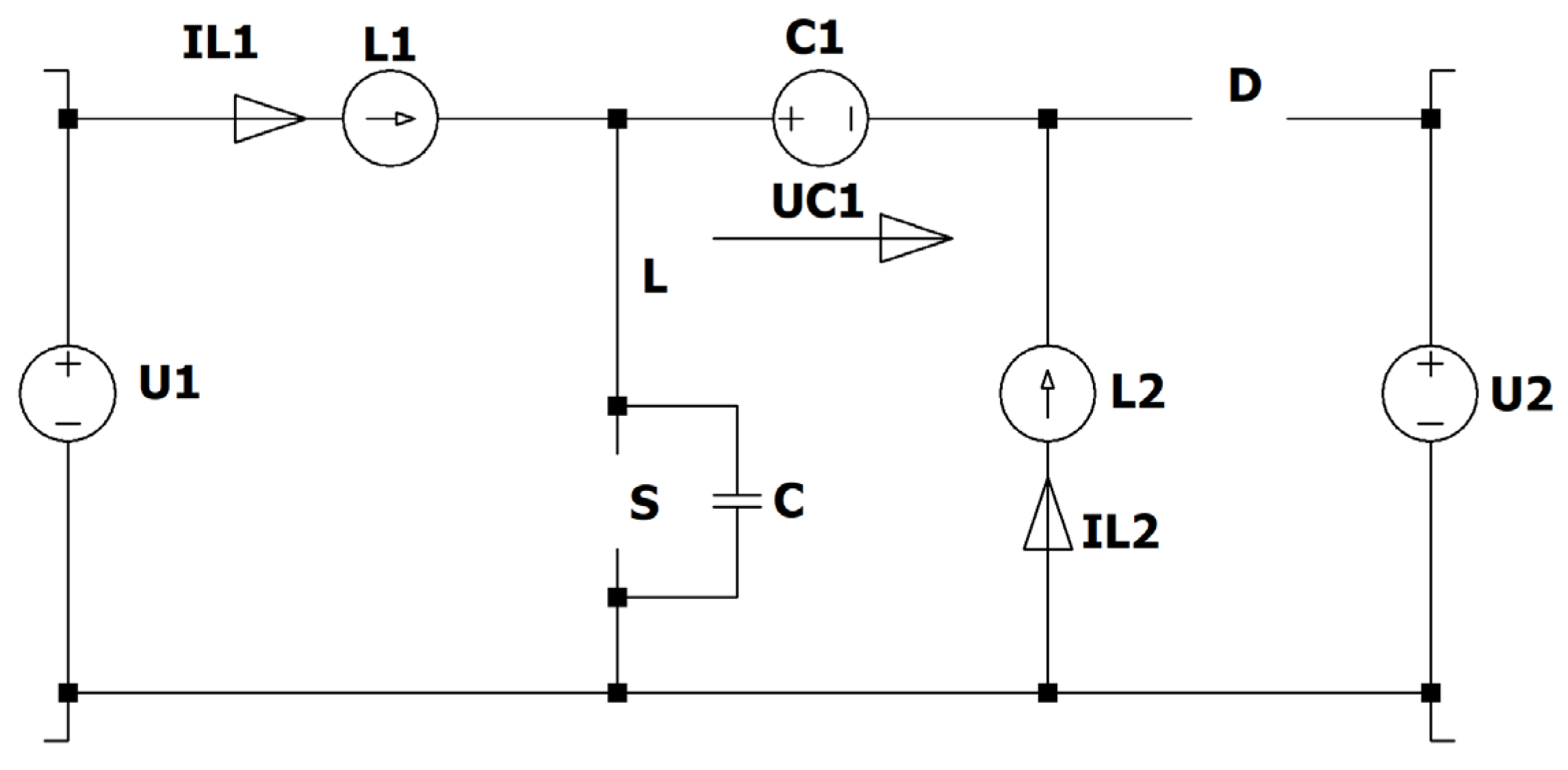
Figure 46.
ZVS QR SEPIC: M2.
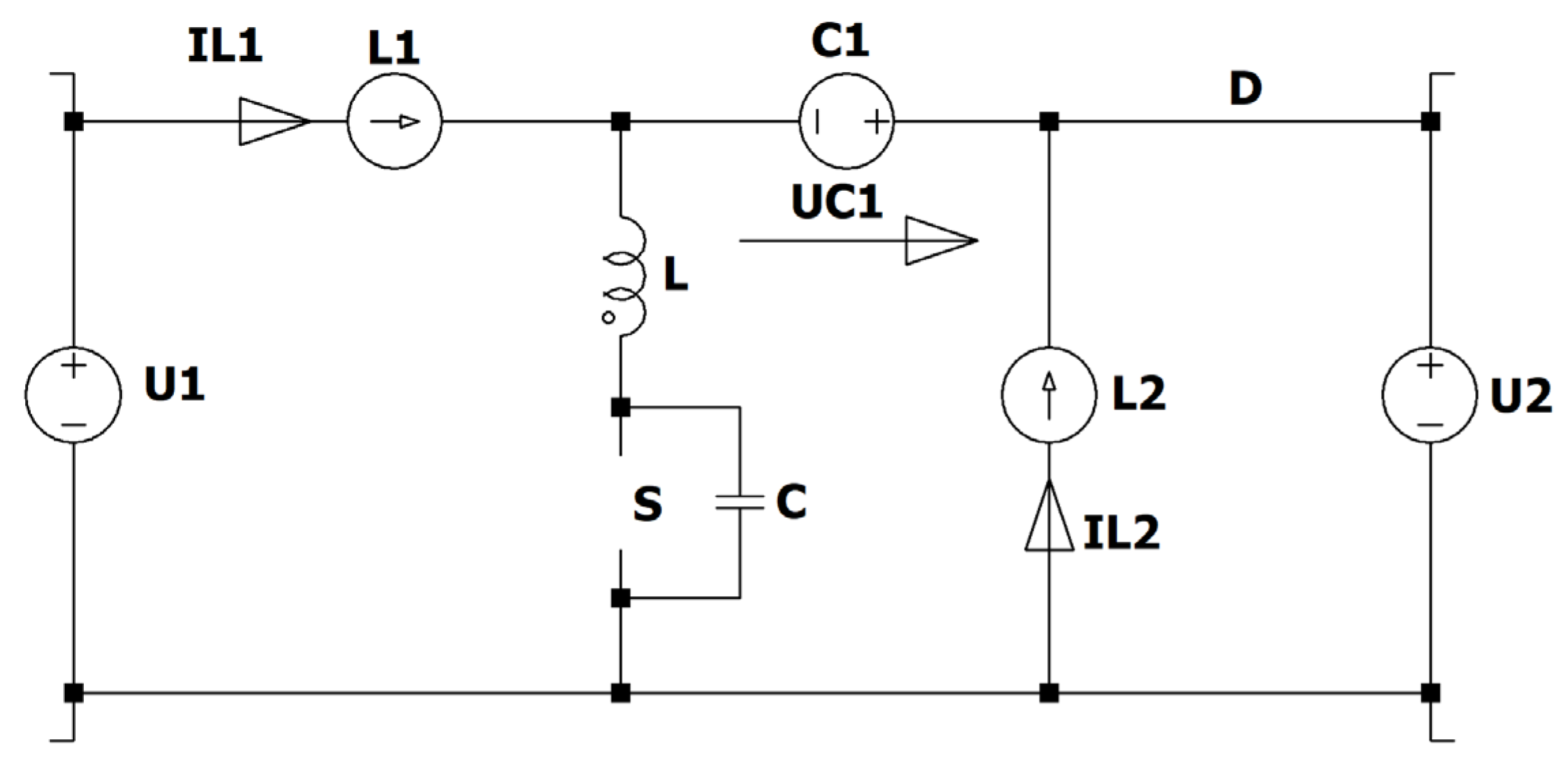
Figure 47.
ZVS QR SEPIC: M3.
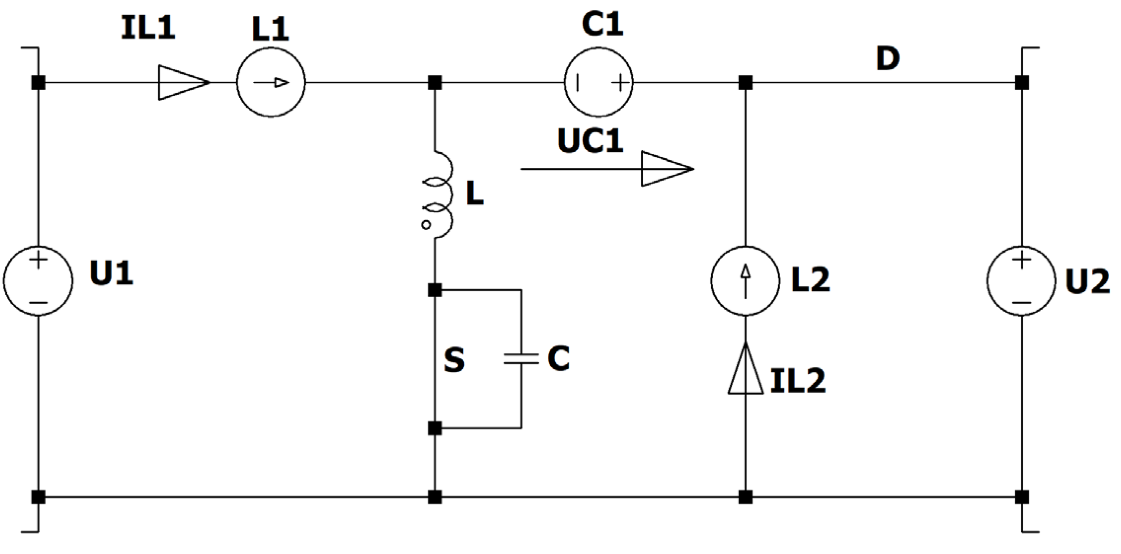
Figure 48.
ZVS QR SEPIC circles describing mode M2: different currents and voltages are shown.
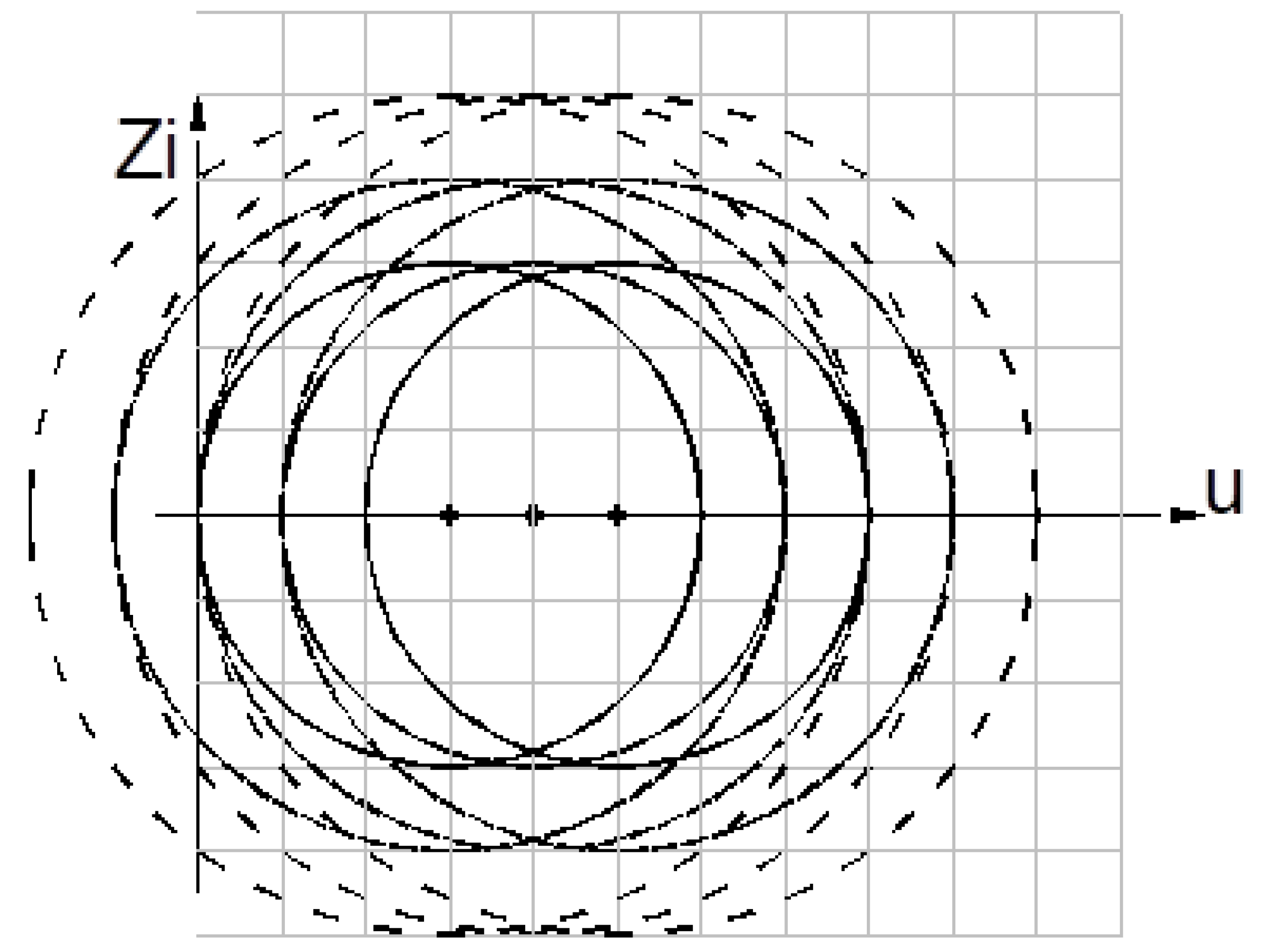
Figure 49.
ZVS QR SEPIC: simulation circuit.
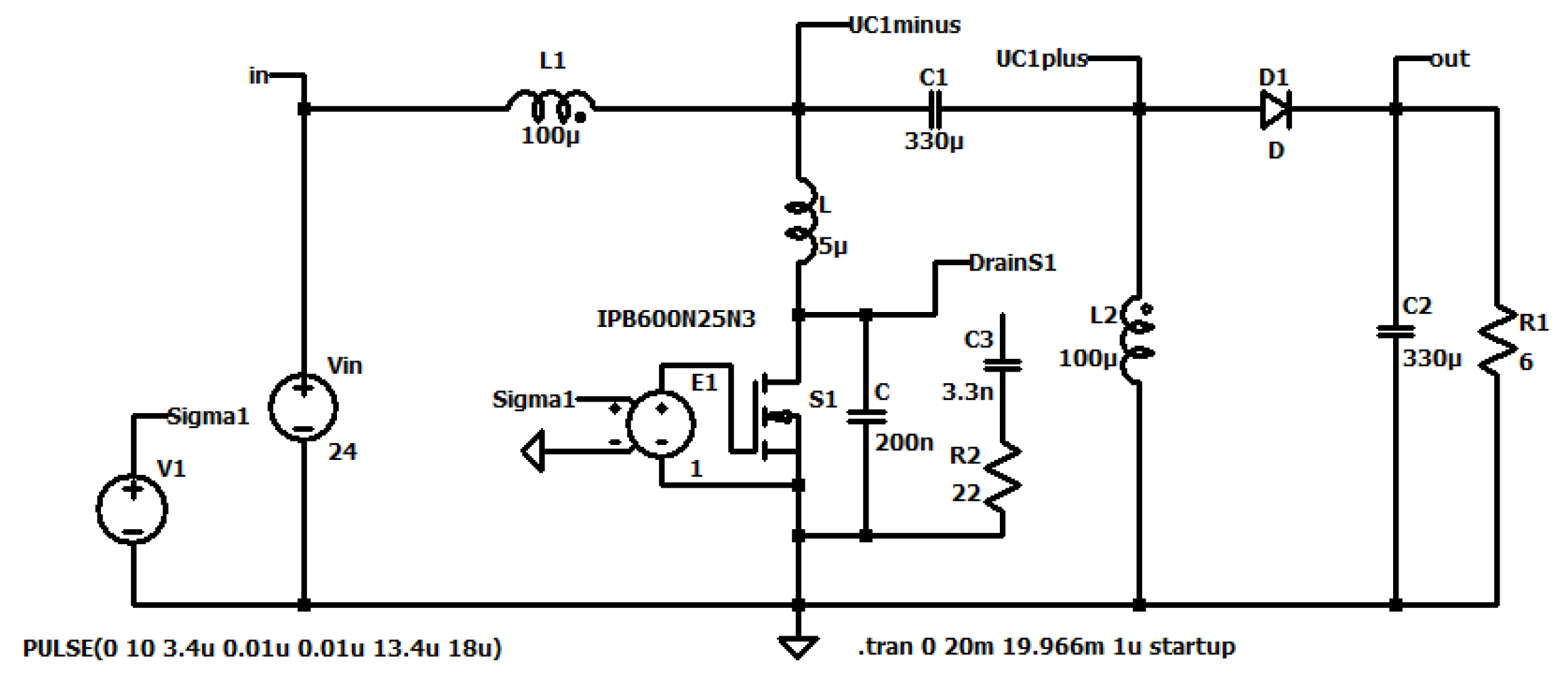
Figure 50.
ZVS QR SEPIC: (a) up to down: voltage across the resonant capacitor (dark green); current through the resonant coil (red), current through the converter coils (violet); output voltage (green), input voltage (blue), control signal (turquoise); (b) u-Zi diagram.
Figure 50.
ZVS QR SEPIC: (a) up to down: voltage across the resonant capacitor (dark green); current through the resonant coil (red), current through the converter coils (violet); output voltage (green), input voltage (blue), control signal (turquoise); (b) u-Zi diagram.
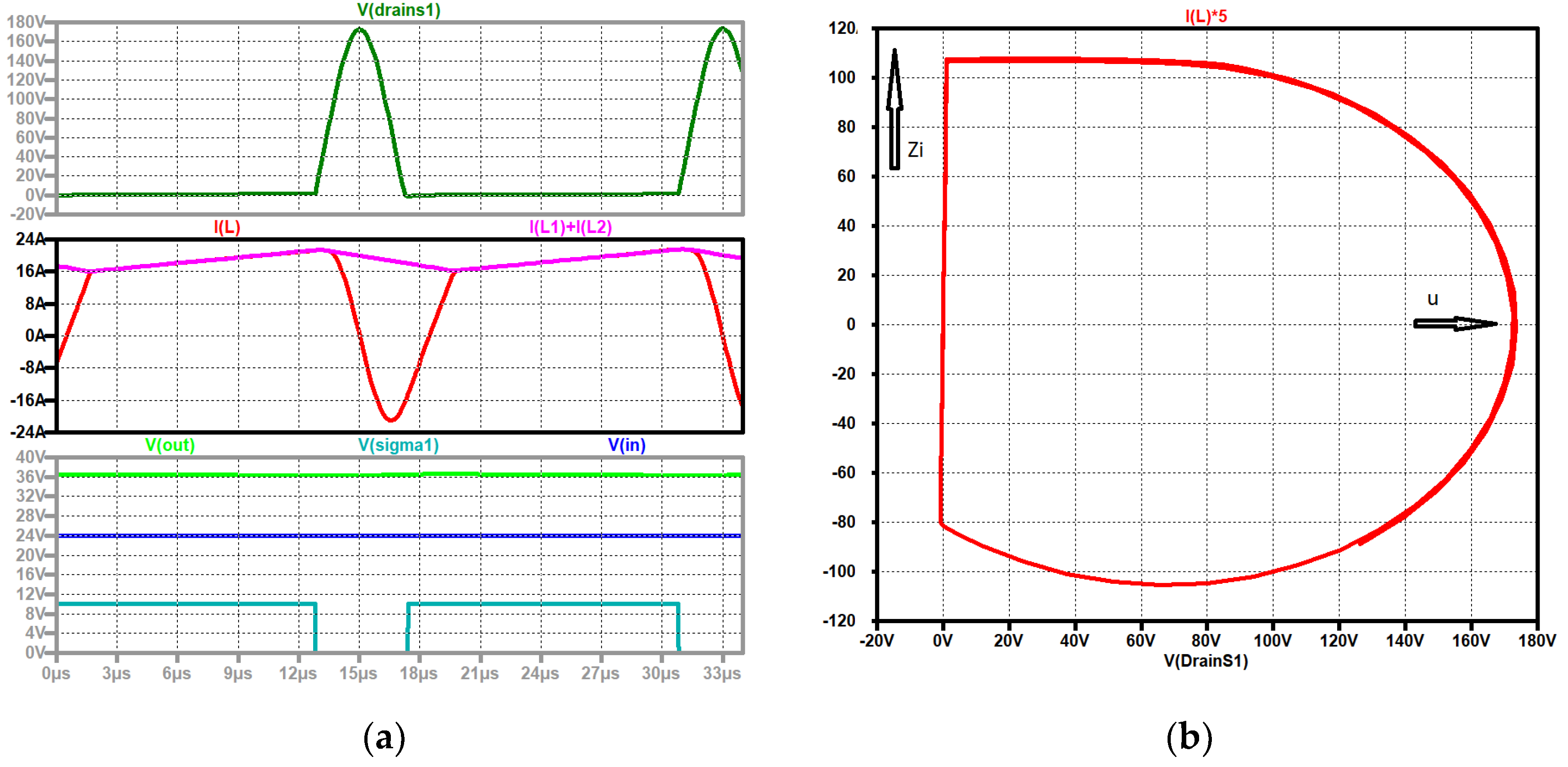
Figure 52.
ZCS QR CUK: (a) mode M0; (b) mode M1.
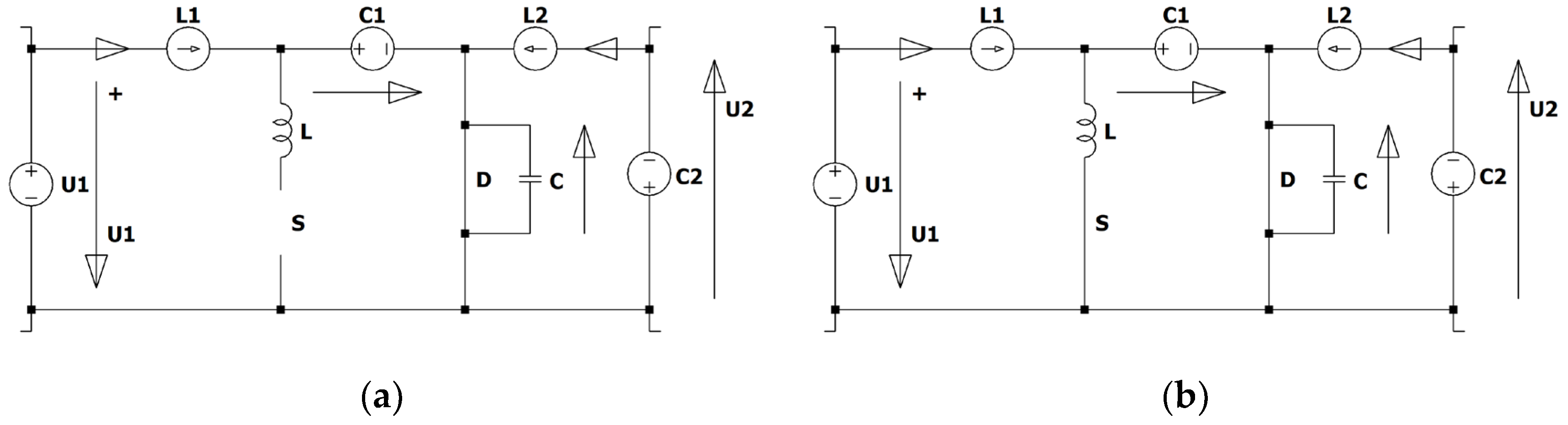
Figure 53.
ZCS QR CUK: (a) mode M2; (b) mode M3.
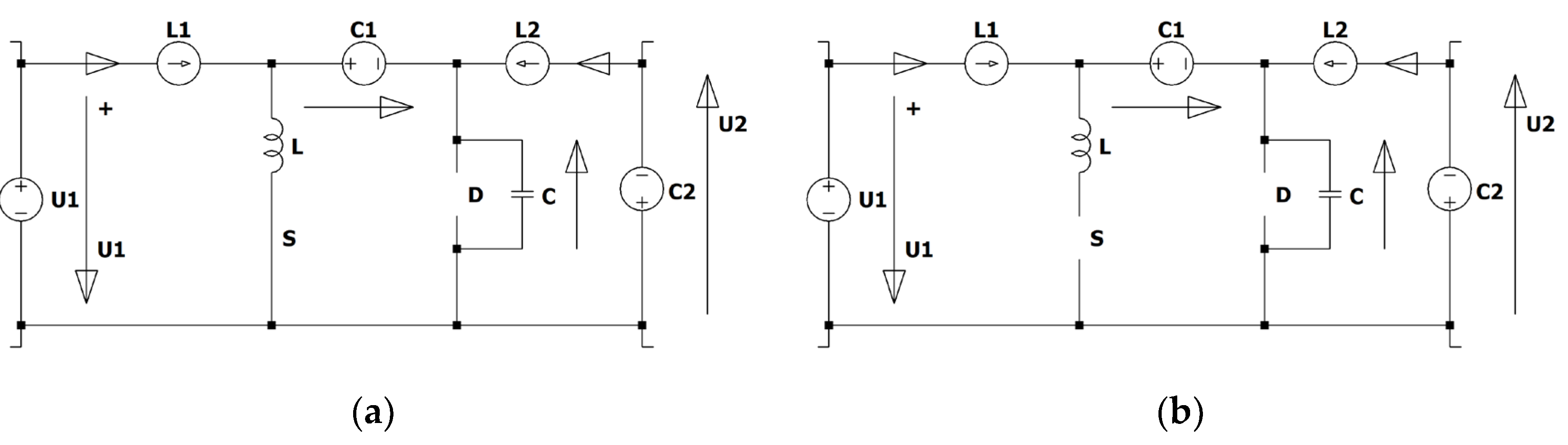
Figure 54.
ZCS QR CUK: (a) simulation circuit; (b) up to down: voltage across the resonant capacitor (green), current through the resonant coil (red).
Figure 54.
ZCS QR CUK: (a) simulation circuit; (b) up to down: voltage across the resonant capacitor (green), current through the resonant coil (red).
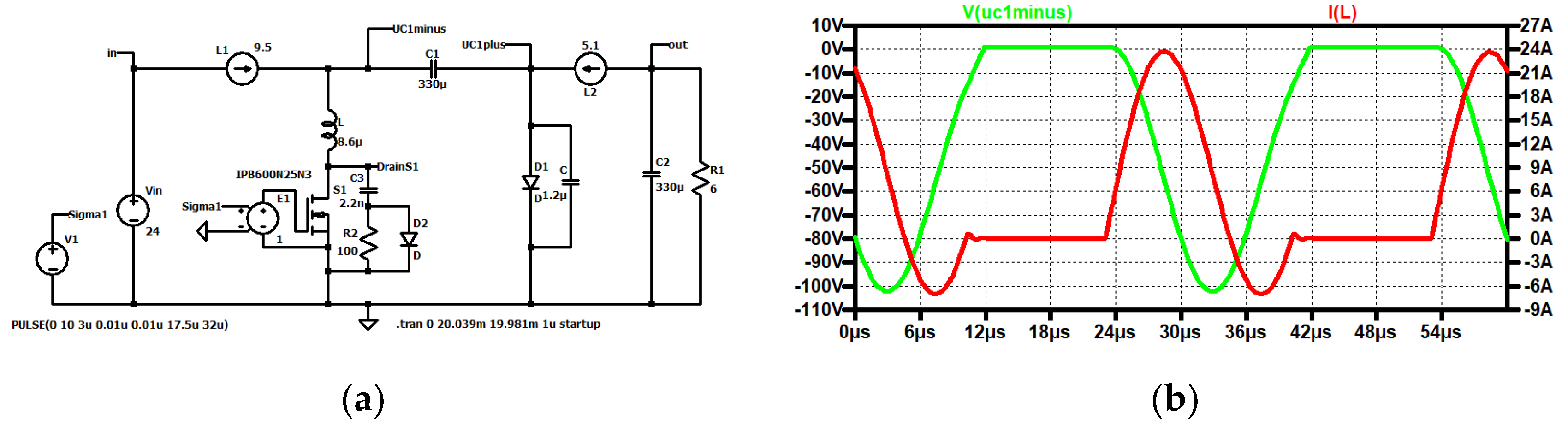
Figure 55.
ZVS QR converter: circuit diagram.
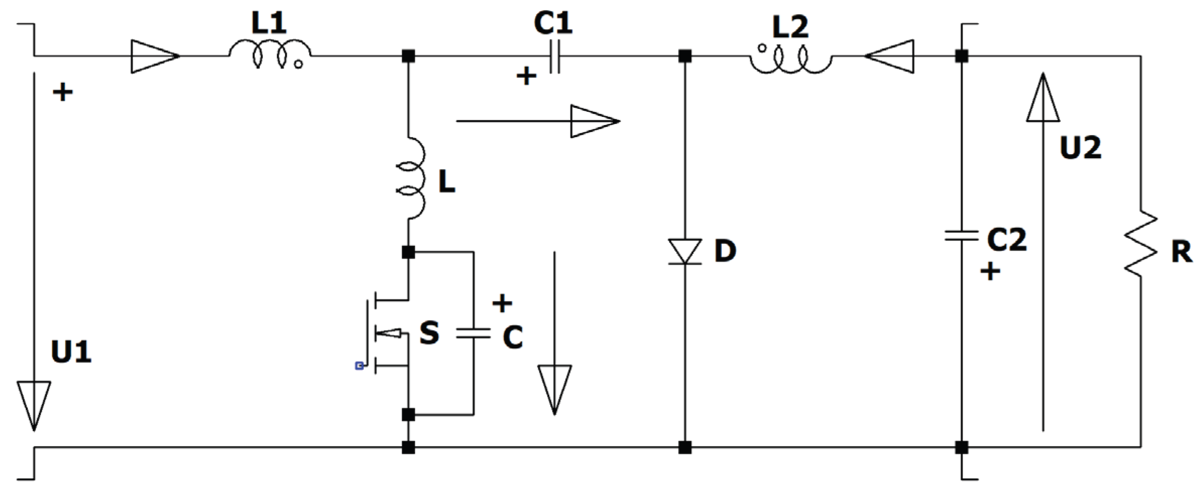
Figure 56.
ZVS QR CUK: (a) mode M0; (b) mode M1.

Figure 57.
ZVS QR CUK: (a) mode M2; (b) mode M3.
Disclaimer/Publisher’s Note: The statements, opinions and data contained in all publications are solely those of the individual author(s) and contributor(s) and not of MDPI and/or the editor(s). MDPI and/or the editor(s) disclaim responsibility for any injury to people or property resulting from any ideas, methods, instructions or products referred to in the content. |
© 2025 by the authors. Licensee MDPI, Basel, Switzerland. This article is an open access article distributed under the terms and conditions of the Creative Commons Attribution (CC BY) license (http://creativecommons.org/licenses/by/4.0/).
Copyright: This open access article is published under a Creative Commons CC BY 4.0 license, which permit the free download, distribution, and reuse, provided that the author and preprint are cited in any reuse.


