Submitted:
15 September 2025
Posted:
17 September 2025
You are already at the latest version
Abstract
Bilayer transition metal dichalcogenides (TMDs) are promising materials for next-generation field-effect transistors (FETs) due to their atomically thin structure and favorable transport properties. In this study, we employ density functional theory (DFT) to compute the electronic band structures and phonon dispersions of bilayer WS2, WSe2, and MoS2, and the electron-phonon scattering rates using the EPW (electron-phonon Wannier) method. Carrier transport is then investigated within a semiclassical full-band Monte Carlo framework, explicitly including intrinsic electron-phonon scattering, dielectric screening, scattering with hybrid plasmon–phonon interface excitations (IPPs), and scattering with ionized impurities. Freestanding bilayers exhibit the highest mobilities, with hole mobilities reaching 2300 cm2/V·s in WS2 and 1300 cm2/V·s in WSe2. Using hBN as the top gate dielectric preserves or slightly enhances mobility, whereas HfO2 significantly reduces transport due to stronger IPP and remote phonon scattering. Device-level simulations of double-gate FETs indicate that series resistance strongly limits performance, with optimized WSe2 pFETs achieving ON currents of 820 A/m, and a 10% enhancement when hBN replaces HfO2. These results show the direct impact of first-principles electronic structure and scattering physics on device-level transport, underscoring the importance of material properties and the dielectric environment in bilayer TMDs.
Keywords:
bilayer TMD
; WS2
; WSe2
; first principles
; DFT
; FET
; device scaling
; dielectric engineering
; short-channel effects
; device performance
1. Introduction
The semiconductor industry has experienced extraordinary growth, initially driven by silicon, which can form large, single-crystal structures ideally suited to modern electronic manufacturing. Since the 1970s, silicon’s advantageous properties and scalability have enabled continuous advancements, allowing transistor densities to increase exponentially—a trend famously captured by Moore’s Law [1]. The miniaturization of silicon-based devices has reduced costs, boosted speed, and lowered power consumption, making it the foundation of digital technology. However, as silicon transistor dimensions have approached their physical limits, it has become challenging to further downscale without encountering fundamental limitations [2,3]. These issues include short-channel effects, increased leakage currents, and degradation of device reliability, which hinder the performance of ever-smaller silicon transistors [4,5].
Motivated by the need for high-performance devices beyond silicon’s capabilities, researchers have turned to alternative materials [6,7,8,9,10]. Since the early 2000s, the search for novel materials to sustain and surpass silicon’s legacy in both classical and unconventional computing has intensified. These new materials, especially those with lower dimensionality, offer unique physical properties that address the challenges faced by silicon at nanoscale dimensions. One class of promising candidates is two-dimensional (2D) materials [11,12,13], which, unlike bulk materials, are formed from layers just one atom thick. These materials exhibit unique electrostatic control due to their thin nature, allowing for reduced short-channel effects and exceptional gate control.
Among two dimentional materials, Transition Metal Dichalcogenides (TMDs) [14,15,16] have garnered significant interest. Structurally TMDs consist of a transition metal layer sandwiched between two layers of chalcogen atoms, with each M-X-M atomic layer forming strong covalent bonds within the layers but weak van der Waals bonds between them. This unique structure enables TMDs to be scaled to atomic thicknesses while maintaining their semiconducting properties, providing a band gap that graphene lacks and allowing for effective switching in field-effect transistors (FETs). The versatility and tunability of TMDs, along with their stable semiconducting properties, make them ideal for future applications in both energy-efficient and high-performance devices.
Bilayer transition metal dichalcogenides (TMDs) offer unique advantages over monolayers for applications in next-generation transistors and electronic devices. They exhibit a higher density of states, enabling greater charge storage, as well as improved carrier mobility for efficient current flow [17,18].Bilayer structures enhance fabrication yields [19] by protecting the bottom layer during processing, minimizing defects, and providing better stability under environmental stress. In particular, WSe2 and WS2 have attracted significant attention for pFET applications due to their intrinsically high hole mobility. With their potential to support further device miniaturization and improved performance, bilayer TMDs represent a promising path for advancing both transistor technology and the broader field of nanoelectronics.
To evaluate the transport properties of bilayer TMDs, it is crucial to consider the dielectric environment, as real-world devices often feature these materials supported by substrates and surrounded by gate dielectrics. This work employs a combination of first-principles and semiclassical computational methods to investigate carrier transport in bilayer TMDs. Density Functional Theory (DFT) and Density Functional Perturbation Theory (DFPT) as implemented in Quantum ESPRESSO [20,21] are used to calculate the full-band electronic structures and phonon dispersions, while electron–phonon scattering rates are obtained using the Electron–Phonon Wannier (EPW) [22,23,24] approach. These first-principles results are incorporated into semiclassical full-band Monte Carlo simulations, solving the Boltzmann transport equation and accounting for intrinsic electron–phonon scattering, screening by the dielectric environment, scattering with the hybrid plasmon/phonon interface excitations, and with ionized impurities. By addressing these critical factors, this study provides a robust framework for understanding and optimizing the electronic transport properties of TMDs, helping their integration into next-generation nanoelectronics.
Our discussion is organized as follows: Section 2 outlines the geometry of the double-gate transistor considered and the theoretical framework underlying our study. Section 3 and Section 4 describe the physical models used for the band structure, phonon dispersion, and electron–phonon scattering rates, as well as the treatment of IPP and impurity scattering. Finally, Section 5, Section 6, and Section 7 present and analyze our transport and FET results.
2. Device Geometry and Monte Carlo Simulation Framework
In our work we have considered a double-gate field-effect transistor (FET) structure with a bilayer TMD as the channel material, shown in Figure 1. The device has a nm channel, with source and drain extensions of equal length nm. The source/drain extensions are doped, while the channel is left undoped. A self-aligned nm gate is centered on the channel.
The top and bottom gate insulators each result in an equivalent oxide thickness (EOT) of 0.7 nm. This double-gate structure captures the impact of the dielectric environment (substrate and top oxide) on carrier transport, including interface phonons, interface plasmon–phonon (IPP) modes (often improperly called “remote phonons”), and dielectric screening induced by free carriers and by the environment.
Electronic transport is treated by solving the two-dimensional Boltzmann Transport Equation (BTE) self-consistently with the Poisson equation using an ensemble Monte Carlo (MC) method. The BTE describes how the carrier distribution evolves over time in real and momentum space under electric fields and scattering. We assume the device to be infinitely wide, such that the gate is much wider than the channel length; this allows us to solve the 2D Poisson equation and neglect edge effects.
The electrostatic potential is obtained by solving the 2D Poisson equation, which accounts for charge distribution and material permittivity. This solution updates the electric field profile used for carrier trajectories in the Monte Carlo simulation. The spatial domain is discretized using non-uniform meshes: one along the transport direction (x) and another along the out-of-plane direction (z), which is refined near the TMD and oxide interfaces. The Poisson equation is solved using the finite element method adapted from [25] with the following form:
where is the electrostatic potential, is the charge density, is the doping profile, and is the electron density. The dielectric tensor is defined piece-wise for each element. In the TMD, we use an anisotropic dielectric tensor:
where and are the in-plane and out-of-plane dielectric constants, respectively. In contrast, the oxide layers use isotropic dielectric constants. The TMD is discretized along z using two mesh elements, each of thickness , where d is the total bilayer thickness. The cloud-in-cell method [26] is employed to map the charge of Monte Carlo particles onto the grid nodes at the center of the TMD layer. Dirichlet boundary conditions are assumed at the source and drain terminals, while Neumann conditions are applied elsewhere.
The MC algorithm alternates between two steps: (i) carriers drift through the device under the electric field and (ii) scattering events are considered based on pre-tabulated rates, which alter energy, momentum, or direction. Carrier positions are then updated, the charge density is recalculated, and the Poisson equation is solved again. Convergence is reached once steady-state transport is established, typically by tracking 2,000–5,000 carriers over several picoseconds to obtain statistically reliable current–voltage and field–energy characteristics. After each MC iteration and before the next free flight, we record carrier energy, velocity, current, charge density, and electrostatic potential. These are ensemble-averaged over the total simulation time:
where is the total simulation time and the i-th free flight duration. In the low-field regime, mobility is extracted from the diffusion constant using the Einstein relation in the non-degenerate limit:
where is the carrier position along the transport direction . This approach minimizes stochastic noise when the drift velocity is much smaller than the thermal velocity. At high fields, the steady-state drift velocity, carrier energy, and field-dependent mobility are computed as
where is the total number of simulated carriers, is the component of the velocity along transport direction (x-axis), and the kinetic energy. Device-level simulations also yield drain current and spatial profiles of charge density, potential, electric field, and carrier energy for each gate and drain bias point. These data allow us to construct I–V characteristics and analyze how scattering mechanisms affect carriers across the device.
We perform Density Functional Theory (DFT) calculations to obtain the bilayer TMD band structure and phonon dispersion. The band structure reveals key electronic properties, such as effective masses and valley configurations that govern carrier kinematics, while the phonon dispersion characterizes the lattice vibrations responsible for intrinsic scattering processes. From these fundamental quantities, we tabulate the rates for electron scattering with the TMD phonons, with IPPs, and with ionized impurities (dopant atoms). The following sections provide details on the scattering mechanisms considered in these simulations.
3. Band Structure and Phonon Spectrum
Band structures of freestanding bilayer TMDs were calculated using density functional theory (DFT) as implemented in Quantum ESPRESSO [20,21]. We employed the Optimized Norm Conserving Vanderbilt (ONCV) pseudopotentials [27] and GGA-PBE exchange-correlation functional [28,29]. The structures were relaxed until atomic forces were below eV/nm, ensuring energy minimization (Figure 2). A vacuum spacing of approximately 1.4 nm was used between supercells to prevent unphysical interlayer interactions.
The phonon dispersions were computed using density functional perturbation theory (DFPT) [30] with a coarse -point mesh of and -point mesh of . To obtain accurate phonon energies, especially for low-energy acoustic modes, Wannier interpolation was performed on a finer mesh using the EPW package [22,23,24]. Spin–orbit coupling (SOC) was included in all calculations as it influences the electronic structure and carrier mobility. The DFT input parameters are summarized in Table 1.
Figure 3 shows the calculated band structure and phonon dispersion of bilayer WS2 along the high-symmetry path M--K-M. Bilayer WS2 exhibits a direct bandgap of 1.56 eV with the conduction band minimum at the K-point and a satellite conduction valley at Q, 58 meV higher in energy. The electron effective masses are isotropic: 0.3 at K and 0.74 at Q. The valence band maximum lies at K with a local maximum at 87 meV lower, with hole effective masses 0.27 at K and 2.1 at .
Previous literature reports bilayer WS2 as an indirect-bandgap material with the conduction band minimum (CBM) at . We observed, however, that the bandgap character strongly depends on the interlayer spacing (Figure 4). At an interlayer distance of 0.68 nm, the CBM shifts to , producing an indirect gap. Reducing the spacing to 0.64 nm lowers the Q valley relative to K, restoring a direct gap between Q and . This sensitivity of valley ordering to interlayer distance highlights the delicate balance between competing conduction-band valleys in bilayer WS2. Even small structural changes such as strain alter the nature of the bandgap.
Experimentally, angle-resolved photoemission spectroscopy (ARPES) can probe the valence bands, but direct identification of the CBM remains challenging. This valley sensitivity has direct consequences for transport, as different conduction-band minima (K, Q, or ) result in varying effective masses, density of states, and intervalley scattering, which can markedly influence carrier mobility and device performance.
4. Scattering Mechanisms
4.1. Electron–Phonon Scattering
Intrinsic electron–phonon scattering is included using first-order perturbation theory. The matrix element for a transition from band m at wavevector to band n at via phonon mode is
where ℏ is the reduced Planck constant, is the frequency of phonon mode at wavevector , and is the change in the self-consistent potential due to the phonon. The electronic eigenstates are used in evaluating the matrix elements. Matrix elements are computed using density functional perturbation theory (DFPT) and interpolated using maximally localized Wannier functions (MLWFs) via EPW [22,23,24]. The scattering rate is obtained using Fermi’s golden rule:
where is the carrier lifetime for phonon mode , is the electron–phonon coupling matrix element, is the Bose–Einstein occupation number representing phonon population, and denotes the energy of the electronic state in band n at wavevector . In all our calculations scattering with out-of-plane acoustic (ZA) phonons is neglected because 2H-phase TMDs possess horizontal mirror () symmetry, which forbids first-order carrier–ZA interactions [31]. Higher-order (two-phonon) processes are much weaker in these materials and therefore contribute negligibly to carrier scattering [32]. The sum over final states accounts for all possible scattering processes to different bands and wavevectors. The final-state density of states is evaluated using a 2D Gilat–Raubenheimer scheme [33,34]. Energy-resolved scattering rates are obtained by summing the contributions from all electronic states within each energy bin and normalizing by the density of states, yielding average rates that are further separated into acoustic and optical phonon contributions. Figure 5 presents phonon-limited scattering rates for electrons (a) and holes (b) in bilayer WS2, showing the contributions of acoustic and optical phonon modes plotted against carrier energy.
4.2. Dielectric Screening
The top and bottom dielectrics (dielectric environment) screen the electron–phonon interaction [35] and a full DFT calculation of the electron–phonon matrix elements for the entire double-gate structure would require an impractically large supercell. To circumvent this, we employ a semi-empirical approach [35]: the matrix elements are first computed for a free-standing 2D layer using Quantum ESPRESSO and EPW. Since the Hartree term dominates the scattering potential, the free-standing Green’s function (implicitly used in DFT) is replaced with one that satisfies the boundary conditions of the double-gate structure, including both dielectrics. This modification rescales the DFT scattering rates by the squared ratio of the two Green’s functions:
where d is the position at the center of the layer (along the z-direction normal to the plane). Here, is the Green’s function of the Poisson equation evaluated at for the dielectric environment of the double-gate geometry, at wavevector Q and phonon frequency . is the corresponding Green’s function for the free-standing layer. The Green’s function incorporates the effect of the 2D electron gas (2DEG) in the TMD layer, so the procedure described also captures free-carrier screening. A thorough discussion of the assumptions behind the scaling factor in Eq. (8) is provided in [35]. Implemented in the Monte Carlo simulations via the rejection method, this rescaling reduces the scattering rates relative to the free-standing case, leading to higher carrier mobility compared to the freestanding layer.
4.3. Interface Plasmon–Phonon (IPP) Scattering
The plasma oscillations of electrons in the bilayer couple with the optical phonons of the top-gate dielectric, the substrate, and the polar 2D layer, giving rise to hybrid interface plasmon–phonon (IPP) modes. This hybridization is particularly important as it significantly affects the scattering rates, especially at small momentum transfer Q. The full theoretical framework is presented in [35] and [36], which provide all necessary details; here, we adopt the notation from [35] and summarize the main results for convenience. Because electron–IPP interactions transfer momentum only through the phonon-like content of each hybrid mode, we must evaluate the phonon content of phonon (TO1, TO2, TO3, TO4, or ZO) for every mode i [37,38]. In terms of this quantity, the scattering potential amplitude for phonon of mode i is given by [35]:
In Eq. ( 9), is the dielectric function of the system. The superscripts high and low correspond to the absence and presence, respectively, of the response from phonon , allowing us to isolate its contribution to the Fröhlich-like potential. A complete derivation of Eq. ( 9) and the resulting scattering rates can be found in Ref. [35].
As discussed in Ref. [35], scattering with interface hybrid excitations controls carrier transport in high- environments. In such dielectrics, this mechanism counteracts the benefits of screening and suppresses the mobility of the 2D channel, often below that of the free-standing case. The reduction becomes more severe as the dielectric constant of the top-gate insulator increases, e.g., when replacing hBN with ZrO2.
4.4. Landau Damping
Landau damping occurs when plasmons fall inside the single-particle excitation continuum, i.e., ( being the Fermi wave vector), so that they are no longer well-defined eigenmodes of the system and decay into incoherent electron–hole excitations. The dielectric response of the 2D TMD monolayer is described by
where and are the static and optical out-of-plane dielectric constants of the monolayer, h is the effective thickness, is the in-plane Fourier transform of the Poisson Green’s function of the device geometry (evaluated at ), is the 2D carrier polarizability given by Stern [39], and is the frequency of the out-of-plane optical (ZO) phonon. In mirror-symmetric (2H) monolayers, the ZO-induced potential is antisymmetric and the electron–phonon matrix element vanishes to first order, so electrons do not couple to this component of the hybrid modes. In the long-wavelength limit (), the carrier contribution in Eq. (10) can be approximated by
where the 2D plasmon frequency is defined as , with n the carrier density and the effective mass. The onset of Landau damping is set by the cutoff wave vector ():
where is the Fermi wave vector. For , plasmons remain coherent and dynamically screen the phonon-like hybrid modes; for , we replace the dynamic long-wavelength term in Eq. 11 with the static Thomas-Fermi expression where is the screening wave vector give by,
with g the valley degeneracy. This framework captures the crossover correctly: Below , plasmons dynamically hybridize with phonon-like modes, whereas above , only statically screened phonon-like branches survive. We consider two double-gate dielectric configurations — hBN/bilayer TMD/SiO2 (low-) and HfO2/bilayer TMD/SiO2 (high-) — to capture the range of remote phonon scattering effects expected in realistic device environments. Figure 6 shows the dispersion of fully hybridized IPP modes in the SiO2/WS2/HfO2 stack, revealing strong phonon-plasmon coupling at small wave vectors Q. Above the Landau damping cutoff , plasmons are suppressed and only surface optical (SO) phonons remain.
Figure 7 shows the hole-IPP scattering rates separated by wave vector regimes ( for hybridized modes and for decoupled SO modes). Scattering is dominated by long-wavelength hybridized modes, especially in the HfO2 configuration due to stronger coupling. In contrast, the hBN stack has weak IPP scattering due to its weak coupling.
Overall, these results underscore the fundamental mobility trade-off when employing high- dielectrics, such as HfO2: While they provide stronger electrostatic gate control, this advantage is offset by increased remote phonon scattering that degrades carrier mobility. Since IPP scattering rates depend on the local carrier density—which varies spatially within a FET—we pre-tabulate these rates for five carrier densities ranging from to cm−2. During the Monte Carlo simulations, the local carrier density at each point is used to interpolate the appropriate IPP scattering rate on a logarithmic scale, ensuring accurate representation of spatially varying IPP rates.
4.5. Impurity Scattering and Dielectric Impact
The impact of charged impurities in the TMD channel is evaluated by solving the Poisson Green’s function for the double-gate geometry considered in this work, following Ref. [40]. The corresponding screened Coulomb potential for a charge located at the bilayer center is expressed as,
where represents the static electronic polarizability of the 2D system, originally formulated by Stern [41] at zero temperature and later generalized to finite temperatures by Maldague [42], and denotes the Fourier transform of the Poisson Green’s function evaluated with the source charge located at the center of the 2D layer [40]:
where T the temperature, is the zero temperature polarizability, the Fermi level and is the Boltzmann constant. Lastly, the impurity scattering rate corresponding to an impurity concentration can be expressed as
The impact of impurity scattering is strongly modulated by the choice of gate dielectric. High- top oxides, such as HfO2, enhance dielectric screening because their large dielectric constant reduces the electric field generated by impurities. This weaker Coulomb field lowers the scattering strength experienced by carriers, thereby improving impurity-limited mobility. However, as disccused in the previous section, a high- dielectric environment also strengthens interface plasmon–phonon (IPP) scattering in the channel, which can significantly degrade carrier mobility. In contrast, low- dielectrics like hBN do not amplify IPP scattering as strongly, and in such cases impurity scattering may be the dominant mechanism depending on the carrier density. This interplay between IPP and impurity scattering has been studied studied previously [43]. Figure 8(a), adapted from [43], shows that with a HfO2 top-gate insulator, IPP scattering dominates transport across the entire range of impurity concentrations, whereas in the case of a low- hBN top insulator, its influence becomes significant only when the impurity density is below the mid-1011 cm−2 level.
5. Electronic Transport in Bilayer Transition Metal Dichalcogenides
This section presents the carrier transport properties of bilayer transition metal dichalcogenides (TMDs). Table 2 and Table 3 report the calculated hole and electron mobilities at a carrier density of cm−2 and K for freestanding bilayers and for double-gated structures with hBN or HfO2 as the top dielectric. Previous theoretical reports [44] have predicted a high hole mobility in WSe2 and WS2. Similary, in our study we found particularly high hole mobilities for bilayer WS2 and WSe2 underscoring their promise for high-performance devices. At the same time, the introduction of a high- dielectric such as HfO2 significantly reduces the mobility due to enhanced IPP scattering, whereas low- dielectrics like hBN preserve much of the intrinsic transport advantage. A more detailed discussion of these trends is provided below.
Freestanding bilayers exhibit the highest mobilities because carriers scatter only with intrinsic acoustic and optical phonons. For example, we calculate hole and electron mobilities of 2300 cm2/Vs and 161 cm2/Vs for bilayer WS2, and 1300 cm2/Vs and 201 cm2/Vs for bilayer WSe2, respectively.
When hBN is introduced as the top-gate dielectric, mobilities remain close to or in some cases even exceed those of the freestanding case. For instance, the hole mobility in bilayer WSe2 increases from 1300 cm2/Vs to 1500 cm2/Vs, while the electron mobility in WS2 improves slightly from 161 cm2/Vs to 172 cm2/Vs. This beneficial behavior stems from two factors. First, hBN exhibits inherently weak interface plasmon phonon (IPP) scattering due to its low ionic polarization and the high optical phonon frequencies associated with the light B and N ions. Second, hBN provides additional dielectric screening of Coulomb interactions, which further suppresses scattering from charged impurities and enhances transport characteristics. The combined effect of weak IPP coupling and efficient dielectric screening makes hBN an exceptionally favorable dielectric environment for TMD devices [38].
In contrast, HfO2 leads to strong degradation in mobility across all TMDs studied. For WS2, the hole mobility drops from 2300 cm2/Vs in the freestanding configuration to only 100 cm2/Vs, and for WSe2, the electron mobility falls from 201 cm2/Vs to 36 cm2/Vs. This sharp reduction is due to the high dielectric constant and strong ionic polarization of HfO2, which significantly enhance remote phonon and IPP scattering. Although the high- oxide provides strong electrostatic control the additional scattering channels dominate, severely limiting mobility. These findings are consistent with earlier reports [37,45] for TMDs, showing that mobility decreases nearly monotonically as the gate insulator’s dielectric constant increases. While hBN offers the best transport performance and can even outperform the freestanding case in some configurations, it comes with trade-offs such as a low dielectric constant that limits gate capacitance and a relatively small barrier height that could increase gate-leakage currents if used alone as a gate dielectric.
6. Velocity-Field Characteristics
Next, we studied high-field carrier transport for freestanding and double-gated bilayer TMDs (Figure 9 and Figure 10). The drift velocity initially increases linearly with field (Ohmic regime), saturates, and then exhibits negative differential mobility (NDM) at high fields due to carriers populating satellite valleys with heavier effective masses.
For freestanding WS2, NDM occurs near V/cm as holes gain energy to populate the valley with larger effective mass, reducing drift velocity. In HfO2/bilayer WS2/SiO2, increased scattering suppresses energy gain, shifting NDM onset to fields above V/cm. The hBN configuration behaves similarly to freestanding but with slightly delayed NDM.
Bilayer WSe2 exhibits a similar behavior with NDM onset around V/cm in freestanding conditions but delayed under HfO2. Bilayer MoS2 has lower mobility and delayed NDM onset due to stronger intrinsic scattering and dielectric effects, with NDM absent in the HfO2 environment over the field range studied.
In summary, bilayer TMDs exhibit transport strongly modulated by dielectric environment. Freestanding layers achieve the highest mobilities, limited only by intrinsic phonon scattering. Low- dielectrics like hBN moderately reduce mobility by remote phonon scattering, whereas high- materials such as HfO2 drastically degrade mobility due to enhanced interface plasmon-phonon scattering. High-field transport shows NDM related to satellite valley population, which is suppressed by increased scattering in high- stacks. These findings emphasize the critical trade-offs in device design between gate control and mobility retention in bilayer TMD-based transistors.
From the mobility results, it is evident that bilayer WSe2 and WS2 are strong candidates for future FET technologies. Compared to their monolayer counterparts, the bilayers generally exhibit higher hole mobilities (e.g., bilayer WS2: 2300 cm2/Vs vs. monolayer WS2: 750 cm2/Vs) but similar electron mobilities.
7. Bilayer TMD-Based Double-Gate MOSFETs
In this section, we analyze the performance of double-gate MOSFET architectures employing TMD bilayers as channels, focusing on how design choices affect electrostatic control, scattering, and series resistance. As device dimensions scale aggressively into the sub-10 nm regime, maintaining strong gate control is critical. To address this, the semiconductor industry has adopted high- dielectrics such as HfO2, which enable reduced equivalent oxide thickness (EOT) while mitigating gate leakage. While hBN provides low scattering and yields high mobilities, its relatively low dielectric constant makes it less attractive for scaled CMOS technologies. Motivated by this tradeoff, we concentrate on evaluating device performance with HfO2 as the top-gate dielectric, assessing its impact on transport and electrostatics in bilayer TMD channels.
Our first goal is to identify the most promising device architecture. We begin with a 30 nm long double-gate nFET based on bilayer WSe2 and HfO2 as the top oxide. In our discussions, we will first study the electrostatics of this baseline device using phonon-limited transport. For the final device design, we include the complete scattering set (phonon, interface plasmon phonon, impurity) and evaluate multiple configurations involving HfO2 and hBN as top oxides, and bilayer WSe2 and WS2 as channels for both nFET and pFET.
The first design is a double-gate n-type MOSFET with bilayer WSe2 as the channel and HfO2 as the top gate oxide, shown in Figure 1. The device has a channel length of nm and source/drain extensions of nm. The channel is intrinsic, and the source/drain regions are degenerately doped. A self-aligned top gate of nm is centered over the channel. The EOT is given by:
Assuming a 0.7 nm EOT and using HfO2 (), the physical oxide thickness is nm. Figure 11 shows the transfer characteristics at V and V. The device achieves an on-current A/m at V, a threshold voltage V, and a subthreshold slope (SS) of ≈ 89 mV/dec.
In scaled FETs with high- dielectrics, electrostatics can be affected by strong fringing fields at the gate edges. These are electric field lines that do not pass vertically through the channel but instead fringe laterally into the source and drain regions. Fringing fields degrade short-channel performance by distorting the potential profile and weakening gate control. TMDs like bilayer WSe2 have high out-of-plane permittivity (–15) and low in-plane permittivity (–7), which amplifies fringing field penetration through the high- gate dielectric. As noted in [46,47], this results in stronger short-channel degradation especially increased DIBL and worse SS.
Figure 12 (a) shows the potential energy profile along the channel. The steep potential profile near the drain end at higher , corresponds to electric fields that exceed the Ohmic region. In Figure 12 (b), the average electron kinetic energy increases near the drain for higher biases, exceeding 250 meV at V. This corresponds to substantial carrier heating in high-field regions. As dicussed in Section 4.3, IPP scattering is very strong in high-k dielectric environment. But, we need high- to maintain the gate control. A solution to mitigate this issue is using low- spcaer dielectric in the source and drain region but keeping the high- HfO2 above the channel region. So, we introduced low- SiO2 spacers in the source/drain extensions and extended the drain length to 30 nm Figure 13 to also allow the carriers to cool before reaching the contact.
Figure 14 shows the transfer characteristics of the large-drain device with spacers and only phonon scattering. We observe marginal improvement in subthreshold swing (SS ≈ 84 mV/dec). However, the extended drain region introduces parasitic resistance that reduces both the ON-current () and transconductance.
While these results account only for intrinsic phonon scattering, additional scattering mechanisms such as interface plasmon phonons are expected to further degrade by increasing the total series resistance. Figure 15 shows the spacers comparison transfer characteristics of the large-drain device with phonon and IPP scattering included. As expected we see improvement in with the low-k spacers. At low bias we see higher current for the device without spacers owing to the fringe-induced barrier lowering (FIBL) as discussed in [47].
High remains a critical performance metric for logic transistors, as it directly influences switching speed, drive strength, and energy efficiency. A higher enables faster charging and discharging of load capacitances, reducing gate delay and improving overall circuit throughput. Maintaining high drive current is critical for ensuring fast switching and high performance in scaled logic devices, while also improving power efficiency by reducing switching delays [48,49,50].
To improve , reducing source/drain extension length is necessary to suppress parasitic resistance, as shown in Figure 16, which illustrates the final device design with shorter source/drain extensions. This design choice, however, comes at the cost of increased hot carrier generation. Hot-carrier degradation in aggressively scaled devices is a well-characterized reliability challenge. However, comprehensive modeling of HCD under various bias conditions enables designers to predict degradation and implement mitigations early in the design process [51,52].
To quantify the impact of various scattering mechanisms on device performance, we simulate pFETs with increasing scattering complexity: starting with only bulk phonons, then adding interface plasmon phonon (IPP) scattering, and finally including impurity scattering. We use pFETs for this analysis because bilayer WSe2 exhibits higher hole mobility, leading to higher baseline values—making the impact of added scattering mechanisms more evident. As shown in Table 4, the long-channel (30 nm drain) pFET suffers a sharp drop in from 950 A/m to 283 A/m as scattering increases. In contrast, a short-channel (5 nm drain) pFET with all scattering mechanisms still delivers a high of 820 A/m, demonstrating that aggressive scaling can recover performance even under significant scattering.
Finally, we present all the results for a ultra short device with 5nm source and drain extension. Figure 17 and Figure 18 show the I–V characteristics of bilayer WSe2 nFETs and pFETs, comparing devices with hBN and HfO2 as top gate dielectrics and SiO2 spacers.
Table 5 and Table 6 summarize the ON-current, transconductance, and SS for short-drain nFET and pFET designs based on bilayer WSe2 and WS2. Using HfO2 as the top gate insulator and including all scattering mechanisms (bulk phonons, IPP, and impurity), the best performance was achieved with the SiO2–HfO2–SiO2/bilayer-WSe2/SiO2 pFET, which reached A/m at V. Replacing HfO2 with hBN as the top oxide further improved by to 890 A/m as shown in Figure 19.
8. Conclusions
We have presented a comprehensive investigation of carrier transport and device performance in bilayer transition metal dichalcogenides (TMDs), using full-band Monte Carlo simulations. Our study first examined the low-field mobility and high-field velocity-field characteristics for several bilayer TMDs—including WS2, WSe2, and MoS2—in freestanding and double-gated configurations with hBN and HfO2 dielectrics.
The results clearly show that the dielectric environment plays a pivotal role in modulating transport. Freestanding bilayers exhibit the highest mobilities, limited only by intrinsic phonon scattering. hBN, due to its weak ionic polarization and high phonon energy, retains high mobility and in some cases even improves upon the freestanding case by screening out-of-plane fields while minimally enhancing interface plasmon-phonon (IPP) scattering. In contrast, high- materials like HfO2 drastically degrade mobility due to strong IPP and remote phonon scattering, despite offering better electrostatic control. These trends were observed consistently across all bilayer TMDs studied, reinforcing the importance of dielectric selection in device design. Our FET simulations indicate that scaling down the source/drain extensions significantly improves the ON current () by reducing series resistance, though care must be taken to manage potential reliability issues such as hot-carrier degradation. High-field transport characteristics reveal strong velocity saturation and negative differential velocity (NDV), especially in freestanding and hBN configurations. These effects are suppressed in high- environments due to increased scattering.
By considering HfO2 as the top gate dielectric and accounting for bulk phonon, interface plasmon phonon (IPP), and impurity scattering mechanisms, the optimal device configuration was identified as the SiO2-HfO2-SiO2/bilayer-WSe2/SiO2 pFET with 5 nm source/drain extensions. This setup achieves an ON current () of 820 A/m at V, meeting ITRS performance benchmarks. Replacing the top gate dielectric with hBN leads to a modest increase in to approximately 890 A/m under the same bias conditions, marking a 10% improvement. These findings highlight the critical role of channel-dielectric engineering and device architecture optimization in enhancing the performance of bilayer TMD-based transistors.
In summary, bilayer WSe2 and WS2 could, in principle, enable sub-10 nm FETs that meet the latest ITRS high-performance targets, offering favorable transport and electrostatic characteristics. However, realizing high-performance devices requires careful trade-offs between electrostatic control, mobility degradation, and reliability, as well as attention to fabrication challenges such as high-quality channel growth, gate insulator deposition, and low-resistance contacts. Our results underscore the critical role of accurate physical modeling, including scattering mechanisms and dielectric effects, in guiding the optimization of bilayer TMD-based transistors.
Funding
Funding for this research has been provided by the Taiwan Semiconductor Manufacturing Company Ltd. (TSMC).
Conflicts of Interest
The authors declare no conflicts of interest.
References
- Moore, G.E. Cramming more components onto integrated circuits. Proceedings of the IEEE 1998, 86, 82–85. [Google Scholar] [CrossRef]
- Frank, D.J.; Dennard, R.H.; Nowak, E.; Solomon, P.M.; Taur, Y.; Wong, H.S.P. Device scaling limits of Si MOSFETs and their application dependencies. Proceedings of the IEEE 2001, 89, 259–288. [Google Scholar] [CrossRef]
- Keyes, R.W. Physical limits of silicon transistors and circuits. Reports on Progress in Physics 2005, 68, 2701. [Google Scholar] [CrossRef]
- Wong, H.S. Beyond the conventional transistor. IBM Journal of Research and Development 2002, 46, 133–168. [Google Scholar] [CrossRef]
- Jin, S.; Fischetti, M.V.; Tang, T.W. Modeling of surface-roughness scattering in ultrathin-body SOI MOSFETs. IEEE Transactions on Electron Devices 2007, 54, 2191–2203. [Google Scholar]
- Geim, A.K.; Novoselov, K.S. The rise of graphene. Nature materials 2007, 6, 183–191. [Google Scholar] [CrossRef] [PubMed]
- Das, S.; Robinson, J.A.; Dubey, M.; Terrones, H.; Terrones, M. Beyond graphene: progress in novel two-dimensional materials and van der Waals solids. Annual Review of Materials Research 2015, 45, 1–27. [Google Scholar] [CrossRef]
- Houssa, M.; Scalise, E.; Sankaran, K.; Pourtois, G.; Afanas’ev, V.; Stesmans, A. Electronic properties of hydrogenated silicene and germanene. Applied Physics Letters 2011, 98. [Google Scholar] [CrossRef]
- Vogt, P.; De Padova, P.; Quaresima, C.; Avila, J.; Frantzeskakis, E.; Asensio, M.C.; Resta, A.; Ealet, B.; Le Lay, G. Silicene: compelling experimental evidence for graphenelike two-dimensional silicon. Physical review letters 2012, 108, 155501. [Google Scholar]
- Castellanos-Gomez, A.; Vicarelli, L.; Prada, E.; Island, J.O.; Narasimha-Acharya, K.; Blanter, S.I.; Groenendijk, D.J.; Buscema, M.; Steele, G.A.; Alvarez, J.; et al. Isolation and characterization of few-layer black phosphorus. 2D Materials 2014, 1, 025001. [Google Scholar] [CrossRef]
- Novoselov, K.S.; Mishchenko, A.; Carvalho, A.; Castro Neto, A. 2D materials and van der Waals heterostructures. Science 2016, 353, aac9439. [Google Scholar] [CrossRef]
- Zhang, Z.; Liu, X.; Yu, J.; Hang, Y.; Li, Y.; Guo, Y.; Xu, Y.; Sun, X.; Zhou, J.; Guo, W. Tunable electronic and magnetic properties of two-dimensional materials and their one-dimensional derivatives. Wiley Interdisciplinary Reviews: Computational Molecular Science 2016, 6, 324–350. [Google Scholar] [CrossRef]
- Luo, B.; Liu, G.; Wang, L. Recent advances in 2D materials for photocatalysis. Nanoscale 2016, 8, 6904–6920. [Google Scholar] [CrossRef]
- Mak, K.F.; Lee, C.; Hone, J.; Shan, J.; Heinz, T.F. Atomically thin MoS2: A new direct-gap semiconductor. Physical review letters 2010, 105, 136805. [Google Scholar] [CrossRef]
- Radisavljevic, B.; Radenovic, A.; Brivio, J.; Giacometti, V.; Kis, A. Single-layer MoS2 transistors. Nature nanotechnology 2011, 6, 147–150. [Google Scholar] [CrossRef]
- Larentis, S.; Fallahazad, B.; Tutuc, E. Field-effect transistors and intrinsic mobility in ultra-thin MoSe2 layers. Applied Physics Letters 2012, 101. [Google Scholar] [CrossRef]
- Das, S.; Chen, H.Y.; Penumatcha, A.V.; Appenzeller, J. High performance multilayer MoS2 transistors with scandium contacts. Nano letters 2013, 13, 100–105. [Google Scholar] [CrossRef] [PubMed]
- Kim, S.; Konar, A.; Hwang, W.S.; Lee, J.H.; Lee, J.; Yang, J.; Jung, C.; Kim, H.; Yoo, J.B.; Choi, J.Y.; et al. High-mobility and low-power thin-film transistors based on multilayer MoS2 crystals. Nature communications 2012, 3, 1011. [Google Scholar] [CrossRef] [PubMed]
- Wen, C.; Naylor, C.H.; O’Brien, K.P.; Oni, A.; Kavrik, M.S.; Suh, Y.; Johnson, A. Growth of bilayer transition metal dichalcogenides at controlled locations. APL Materials 2024, 12. [Google Scholar] [CrossRef]
- Giannozzi, P.; Baroni, S.; Bonini, N.; Calandra, M.; Car, R.; Cavazzoni, C.; Ceresoli, D.; Chiarotti, G.L.; Cococcioni, M.; Dabo, I.; et al. QUANTUM ESPRESSO: a modular and open-source software project for quantum simulations of materials. Journal of physics: Condensed matter 2009, 21, 395502. [Google Scholar] [CrossRef]
- Giannozzi, P.; Andreussi, O.; Brumme, T.; Bunau, O.; Nardelli, M.B.; Calandra, M.; Car, R.; Cavazzoni, C.; Ceresoli, D.; Cococcioni, M.; et al. Advanced capabilities for materials modelling with Quantum ESPRESSO. Journal of physics: Condensed matter 2017, 29, 465901. [Google Scholar] [CrossRef]
- Giustino, F.; Cohen, M.L.; Louie, S.G. Electron-phonon interaction using Wannier functions. Physical Review B—Condensed Matter and Materials Physics 2007, 76, 165108. [Google Scholar] [CrossRef]
- Noffsinger, J.; Giustino, F.; Malone, B.D.; Park, C.H.; Louie, S.G.; Cohen, M.L. EPW: A program for calculating the electron–phonon coupling using maximally localized Wannier functions. Computer Physics Communications 2010, 181, 2140–2148. [Google Scholar] [CrossRef]
- Giustino, F. Electron-phonon interactions from first principles. Reviews of Modern Physics 2017, 89, 015003. [Google Scholar] [CrossRef]
- Nagel, J.; Org, N. Solving the Generalized Poisson Equation Using the Finite-Difference Method (FDM) 2011.
- Hockney, R.W.; Eastwood, J.W. Computer simulation using particles; crc Press, 2021. [Google Scholar]
- Hamann, D. Optimized norm-conserving Vanderbilt pseudopotentials. Physical Review B—Condensed Matter and Materials Physics 2013, 88, 085117. [Google Scholar] [CrossRef]
- Perdew, J.P.; Wang, Y. Accurate and simple analytic representation of the electron-gas correlation energy. Physical review B 1992, 45, 13244. [Google Scholar] [CrossRef]
- Perdew, J.P.; Burke, K.; Ernzerhof, M. Generalized gradient approximation made simple. Physical review letters 1996, 77, 3865. [Google Scholar] [CrossRef] [PubMed]
- Baroni, S.; De Gironcoli, S.; Dal Corso, A.; Giannozzi, P. Phonons and related crystal properties from density-functional perturbation theory. Reviews of modern Physics 2001, 73, 515. [Google Scholar] [CrossRef]
- Fischetti, M.V.; Vandenberghe, W.G. Mermin-Wagner theorem, flexural modes, and degraded carrier mobility in two-dimensional crystals with broken horizontal mirror symmetry. Physical Review B 2016, 93, 155413. [Google Scholar] [CrossRef]
- Rudenko, A.; Lugovskoi, A.; Mauri, A.; Yu, G.; Yuan, S.; Katsnelson, M. Interplay between in-plane and flexural phonons in electronic transport of two-dimensional semiconductors. Physical Review B 2019, 100, 075417. [Google Scholar] [CrossRef]
- Gilat, G.; Raubenheimer, L. Accurate numerical method for calculating frequency-distribution functions in solids. Physical Review 1966, 144, 390. [Google Scholar] [CrossRef]
- Vasileska, D.; Goodnick, S.M. Nano-Electronic Devices: Semiclassical and Quantum Transport Modeling; Springer Science & Business Media,, 2011. [Google Scholar]
- Gopalan, S.; Van de Put, M.L.; Gaddemane, G.; Fischetti, M.V. Theoretical study of electronic transport in two-dimensional transition metal dichalcogenides: Effects of the dielectric environment. Physical Review Applied 2022, 18, 054062. [Google Scholar] [CrossRef]
- Hauber, A.; Fahy, S. Scattering of carriers by coupled plasmon-phonon modes in bulk polar semiconductors and polar semiconductor heterostructures. Physical Review B 2017, 95, 045210. [Google Scholar] [CrossRef]
- Fischetti, M.V.; Neumayer, D.; Cartier, E. Effective electron mobility in Si inversion layers in MOS systems with a high-k insulator: The role of remote phonon scattering. J. Appl. Phys 2001, 90, 4587. [Google Scholar] [CrossRef]
- Ong, Z.Y.; Fischetti, M.V. Theory of remote phonon scattering in top-gated single-layer graphene. Physical Review B—Condensed Matter and Materials Physics 2013, 88, 045405. [Google Scholar] [CrossRef]
- Stern, F. Polarizability of a two-dimensional electron gas. Physical Review Letters 1967, 18, 546. [Google Scholar] [CrossRef]
- Ong, Z.Y.; Fischetti, M.V. Charged impurity scattering in top-gated graphene nanostructures. Physical Review B—Condensed Matter and Materials Physics 2012, 86, 121409. [Google Scholar] [CrossRef]
- Stern, E.; Ferrell, R. Surface plasma oscillations of a degenerate electron gas. Physical Review 1960, 120, 130. [Google Scholar] [CrossRef]
- Maldague, P.F. Many-body corrections to the polarizability of the two-dimensional electron gas. Surface Science 1978, 73, 296–302. [Google Scholar] [CrossRef]
- Mansoori, S.; Gopalan, S.; Fischetti, M.V. Mobility Limitations in TMD Monolayers: The Influence of Impurities and Remote Phonons. In Proceedings of the 2023 International Conference on Simulation of Semiconductor Processes and Devices (SISPAD). IEEE; 2023; pp. 33–36. [Google Scholar]
- Ha, V.A.; Giustino, F. High-throughput screening of 2D materials identifies p-type monolayer WS2 as potential ultra-high mobility semiconductor. npj Computational Materials 2024, 10, 229. [Google Scholar] [CrossRef]
- Hess, K.; Vogl, P. Remote polar phonon scattering in silicon inversion layers. Solid State Communications 1979, 30, 797–799. [Google Scholar] [CrossRef]
- Bennett, R.K.; Yin, D.; Yoon, Y. Assessing the role of a semiconductor’s anisotropic permittivity in hafnium disulfide monolayer field-effect transistors. IEEE Transactions on Electron Devices 2020, 67, 2607–2613. [Google Scholar] [CrossRef]
- Bennett, R.K.; Yoon, Y. Exploiting fringing fields created by high-κ gate insulators to enhance the performance of ultrascaled 2-D-material-based transistors. IEEE Transactions on Electron Devices 2021, 68, 4618–4624. [Google Scholar] [CrossRef]
- Cheng, K.; Koswatta, S.V.; Chau, J. Device and circuit considerations for future nanotransistor technologies. IEEE J. Electron Devices Soc. 2019, 7, 1080–1091. [Google Scholar]
- et al., S.K. Design technology co-optimization for beyond-CMOS logic devices. In Proceedings of the Proc. IEEE. 2020; pp. 1–14.
- Nikonov, D.E.; Young, I.A. Benchmarking of beyond-CMOS exploratory devices for logic integrated circuits. IEEE J. Exploratory Solid-State Comput. Devices Circuits 2019, 5, 1–14. [Google Scholar] [CrossRef]
- Tyaginov, S.; Bury, E.; Grill, A.; Yu, Z.; Makarov, A.; De Keersgieter, A.; Vexler, M.; Vandemaele, M.; Wang, R.; Spessot, A.; et al. Compact Physics Hot-Carrier Degradation Model Valid over a Wide Bias Range. Micromachines 2023, 14, 2018. [Google Scholar] [CrossRef]
- Zhou, H. An Overview of Hot Carrier Degradation on Gate-All-Around Nanosheet Transistors. Micromachines 2025, 16, 311. [Google Scholar] [CrossRef] [PubMed]
Figure 1.
Cross-section of the double-gate bilayer TMD FET used in this work.
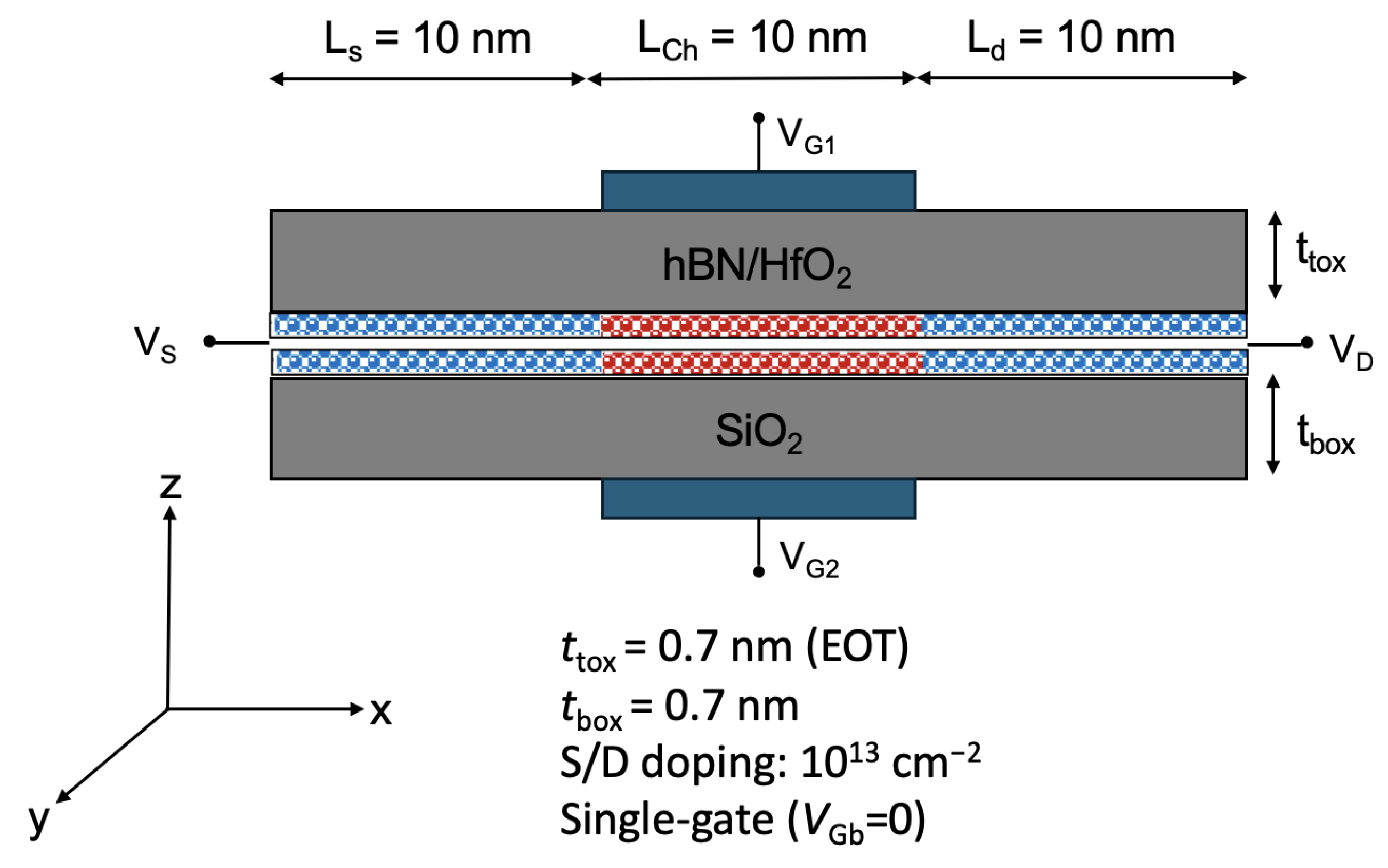
Figure 2.
Relaxed atomic structure of bilayer MoS2.
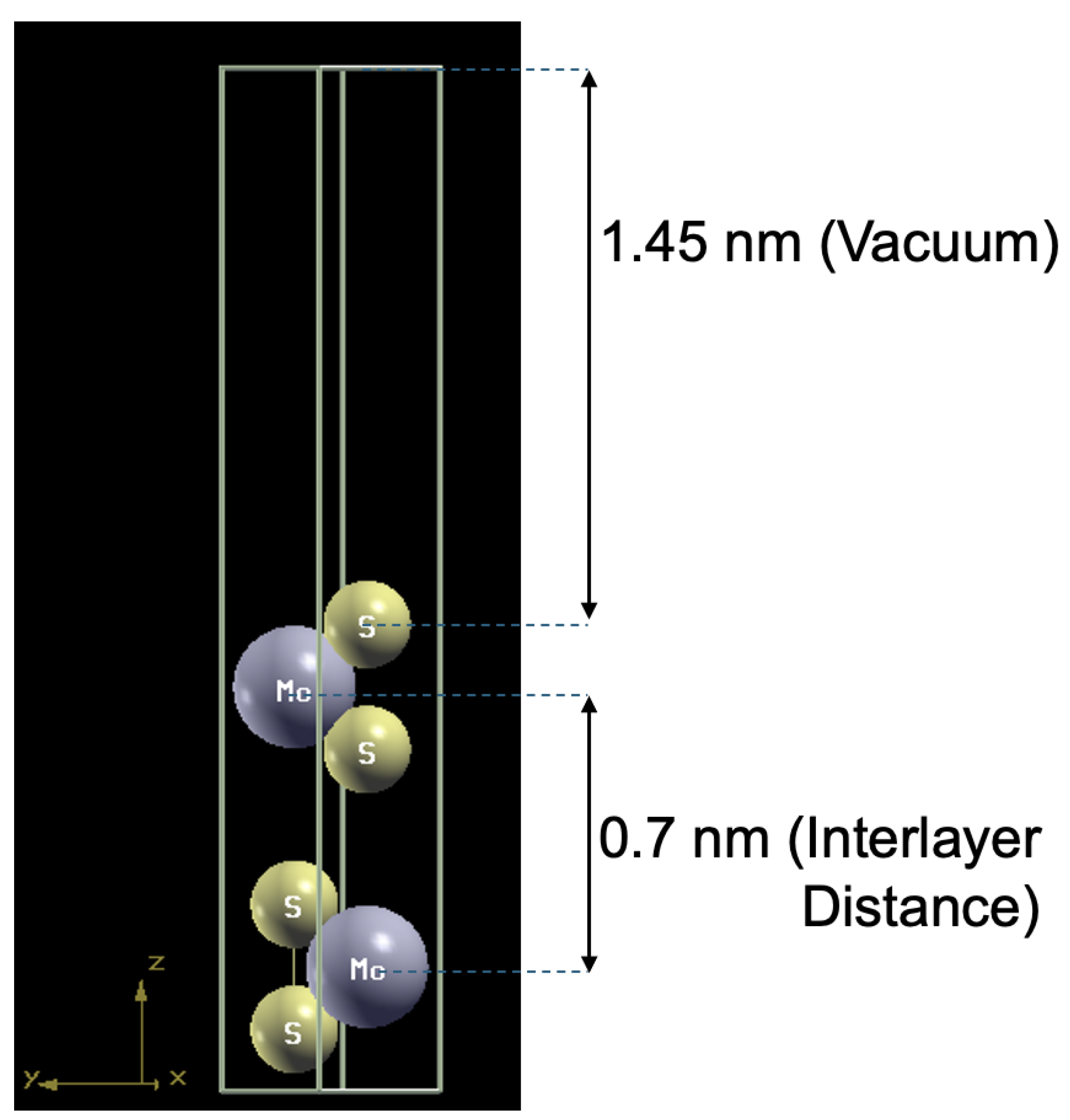
Figure 3.
(a) Band structure and (b) phonon dispersion of bilayer WS2.
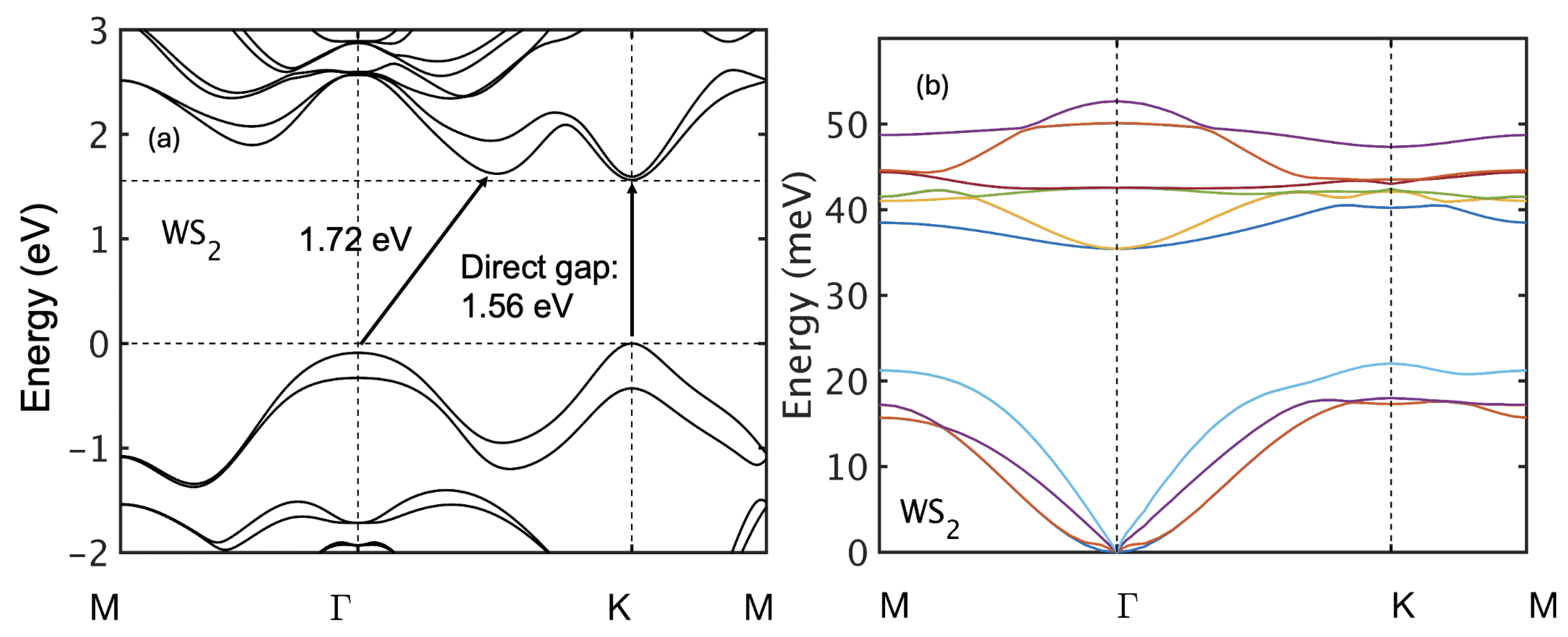
Figure 4.
Effect of interlayer distance on bilayer WS2 band structure: (a) 0.68 nm, (b) 0.64 nm. For smaller interlayer gaps, raises while drops. The gap changes from direct K–K to indirect –K and then to indirect –Q with a further reduction of the interlayer gap.
Figure 4.
Effect of interlayer distance on bilayer WS2 band structure: (a) 0.68 nm, (b) 0.64 nm. For smaller interlayer gaps, raises while drops. The gap changes from direct K–K to indirect –K and then to indirect –Q with a further reduction of the interlayer gap.
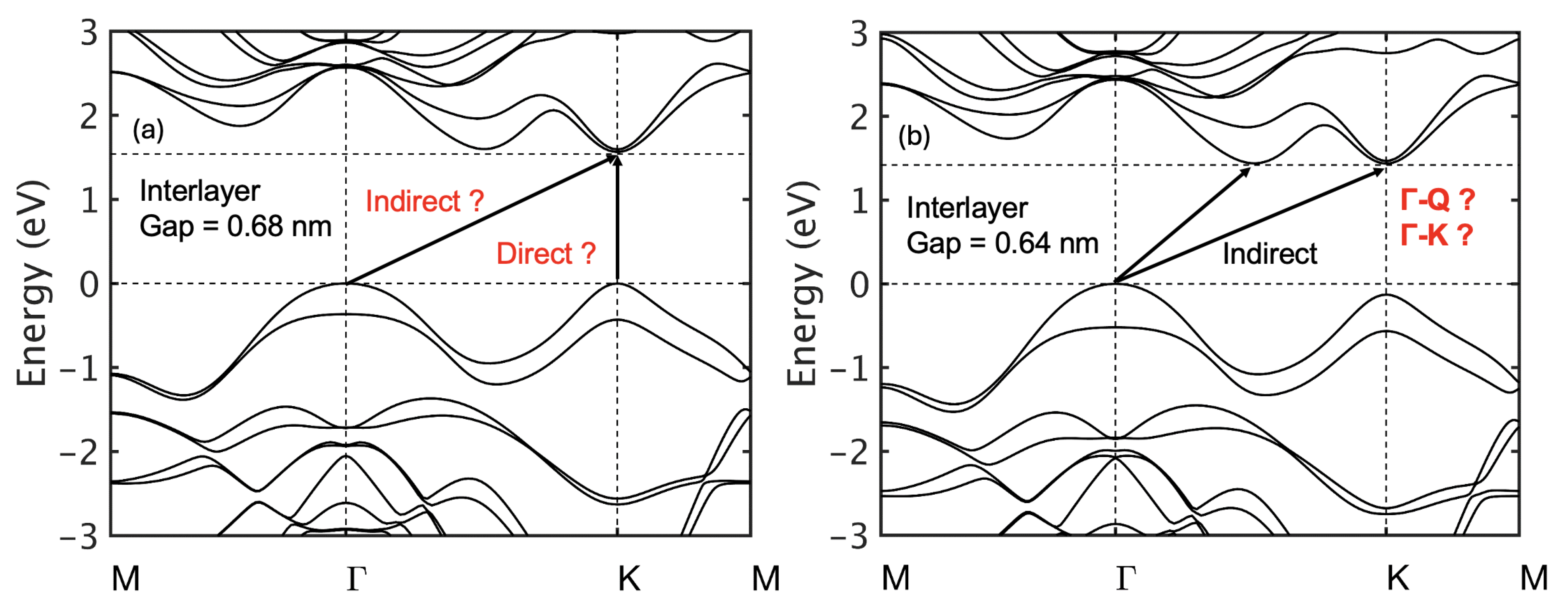
Figure 5.
Phonon-limited scattering rates as a function of kinetic energy for (a) electrons and (b) holes in bilayer WS2. The rates are averaged over equi-energy surfaces, with contributions from acoustic and optical phonons shown separately.
Figure 5.
Phonon-limited scattering rates as a function of kinetic energy for (a) electrons and (b) holes in bilayer WS2. The rates are averaged over equi-energy surfaces, with contributions from acoustic and optical phonons shown separately.
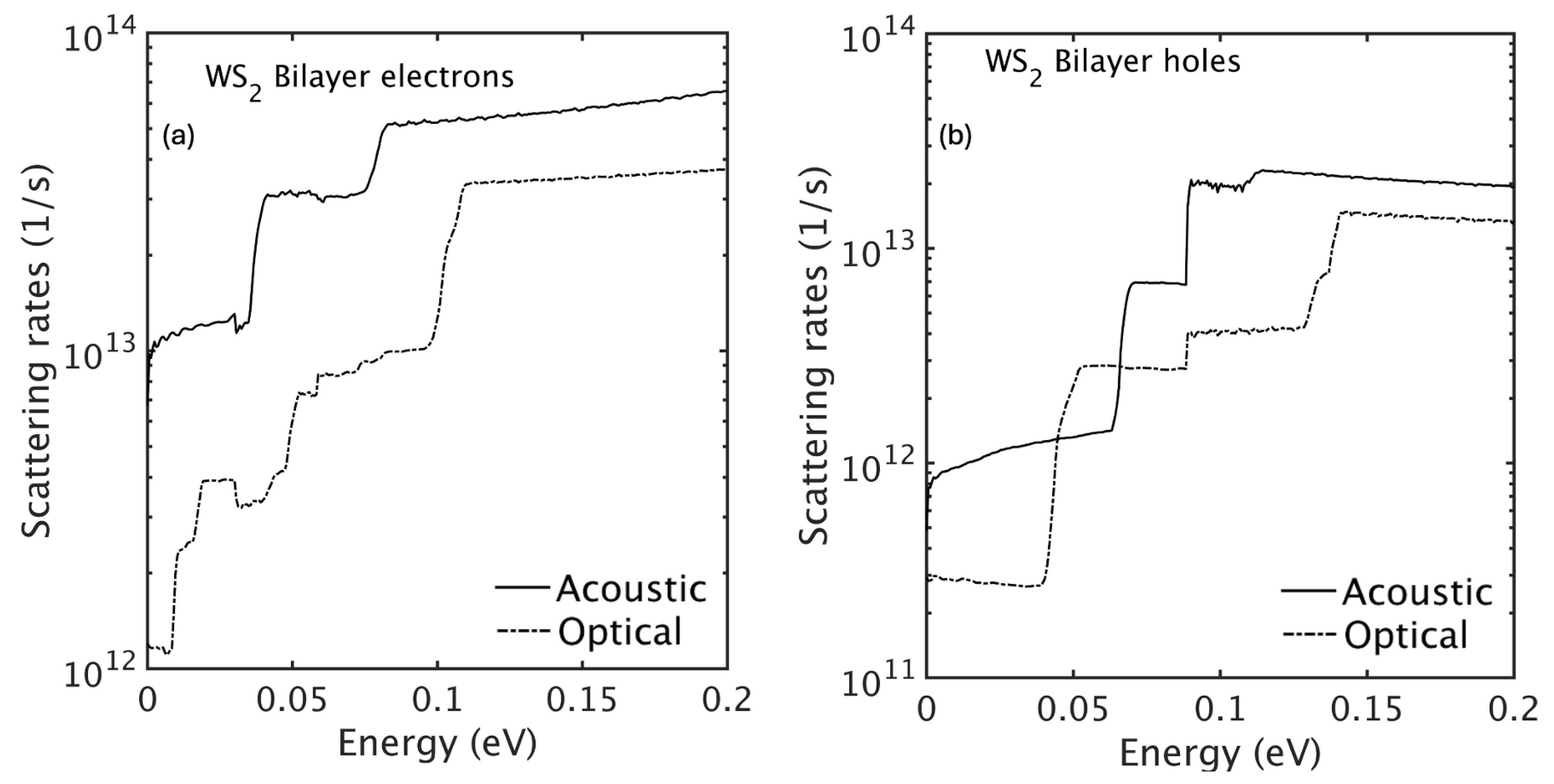
Figure 6.
Dispersion of fully hybridized IPP modes for SiO2/MoS2/HfO2 showing Landau damping cutoff wave vector .
Figure 6.
Dispersion of fully hybridized IPP modes for SiO2/MoS2/HfO2 showing Landau damping cutoff wave vector .
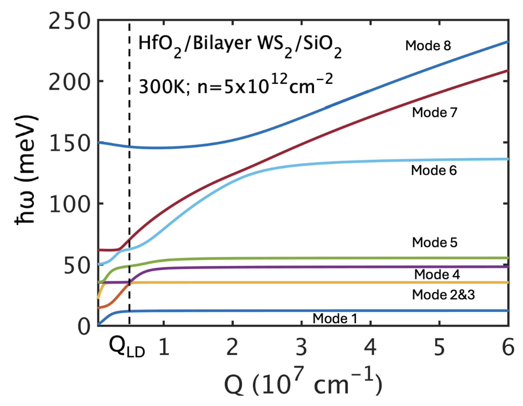
Figure 7.
Electron-IPP scattering rates in bilayer WS2 for (a) (hybridized IPPs) and (b) (surface optical phonons), comparing hBN and HfO2 gate dielectrics.
Figure 7.
Electron-IPP scattering rates in bilayer WS2 for (a) (hybridized IPPs) and (b) (surface optical phonons), comparing hBN and HfO2 gate dielectrics.
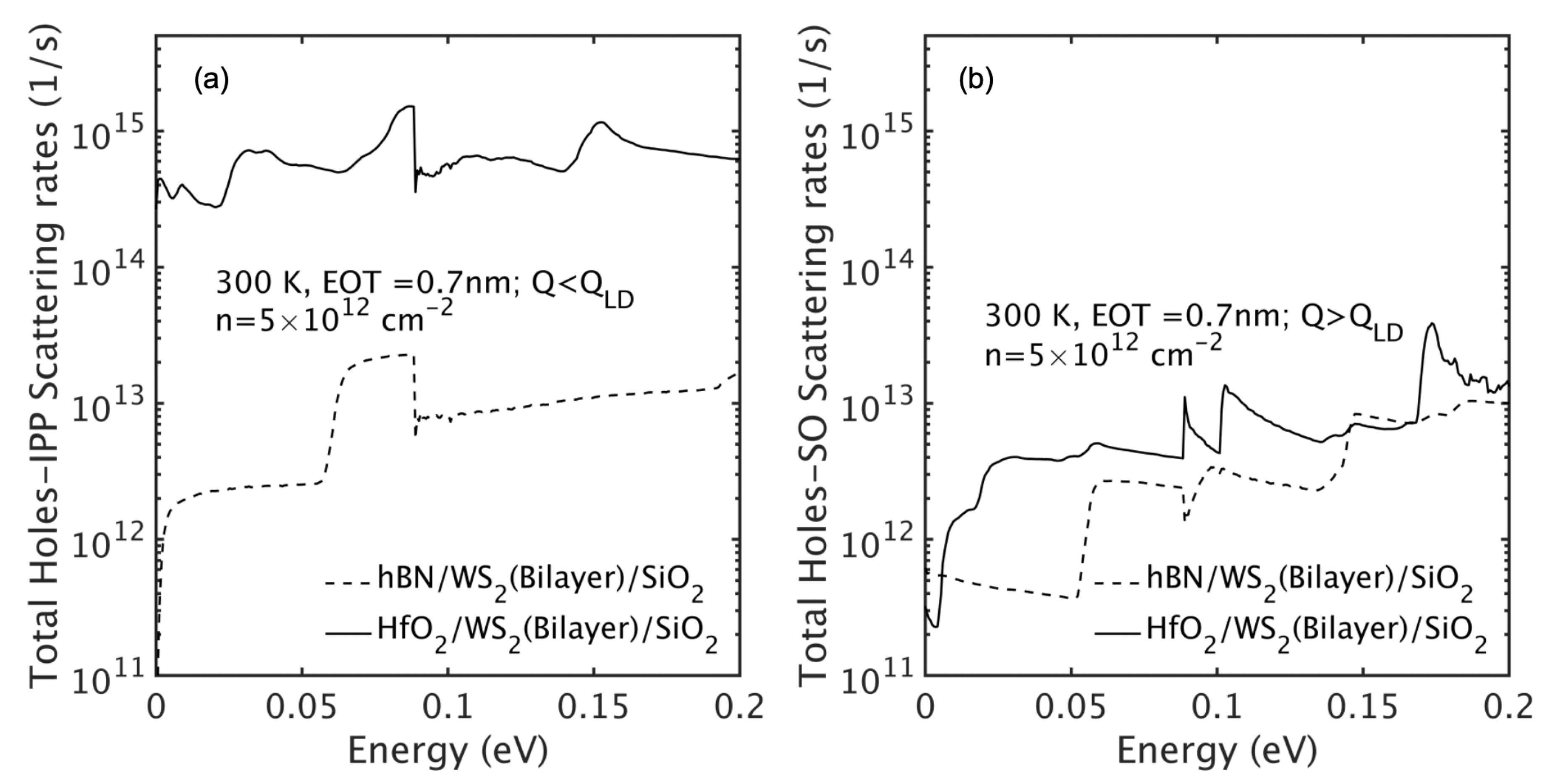
Figure 8.
Dependence of electron mobility on impurity density including different scattering mechanism for the HfO2/WSe2/SiO2 (a) and hBN/MoS2/SiO2 (b) stacks
Figure 8.
Dependence of electron mobility on impurity density including different scattering mechanism for the HfO2/WSe2/SiO2 (a) and hBN/MoS2/SiO2 (b) stacks
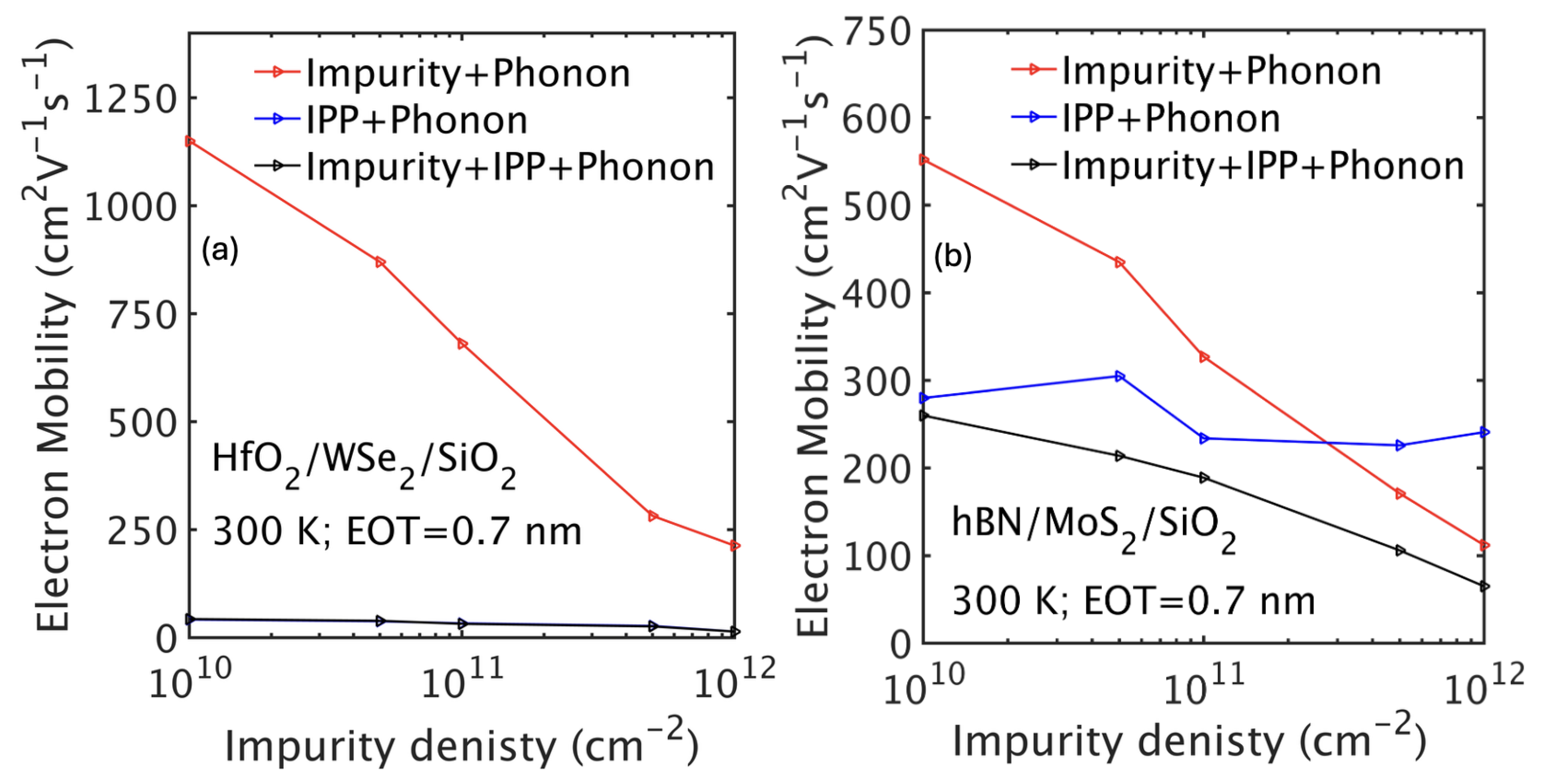
Figure 9.
(a) Hole drift velocity-field and (b) average energy-field characteristics for freestanding and double-gated bilayer WS2. The results have been obtained assuming oxides with an EOT of 0.7 nm and a carrier sheet density of cm−2.
Figure 9.
(a) Hole drift velocity-field and (b) average energy-field characteristics for freestanding and double-gated bilayer WS2. The results have been obtained assuming oxides with an EOT of 0.7 nm and a carrier sheet density of cm−2.
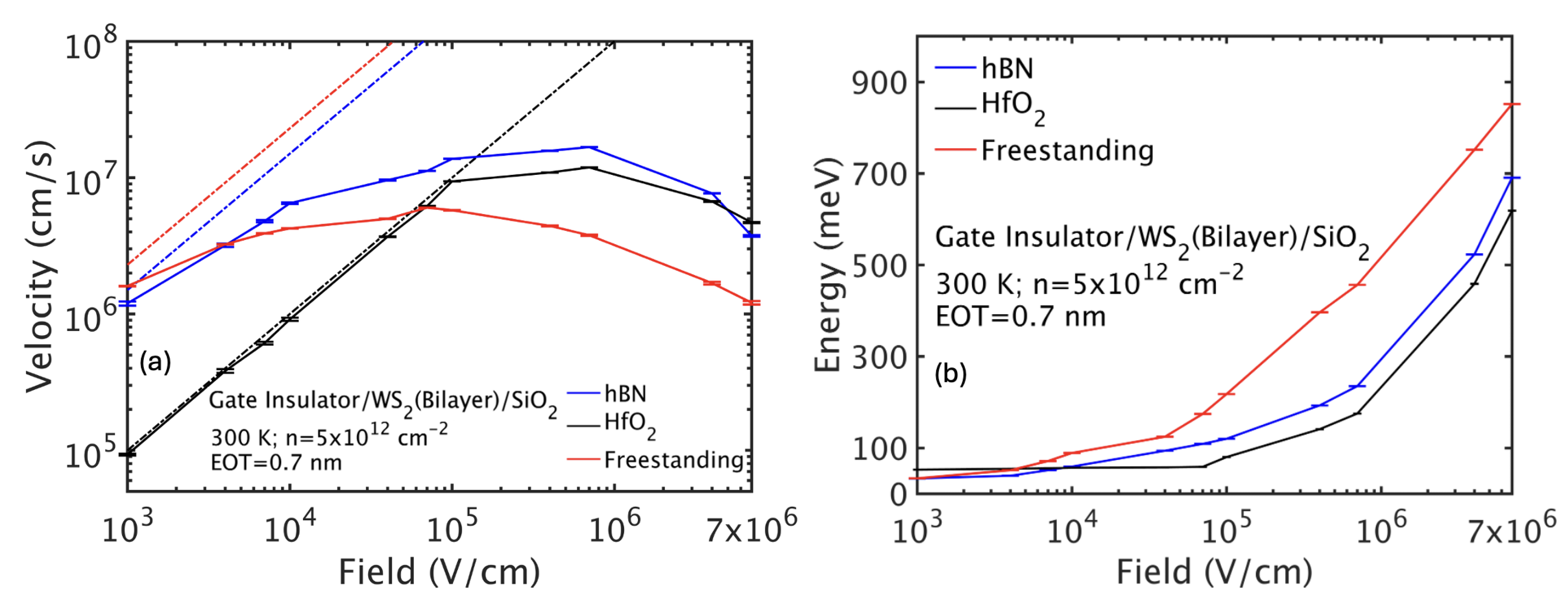
Figure 10.
Hole drift velocity-field and average energy-field characteristics for bilayer WSe2 and MoS2 for free-standing and double gated layers.
Figure 10.
Hole drift velocity-field and average energy-field characteristics for bilayer WSe2 and MoS2 for free-standing and double gated layers.
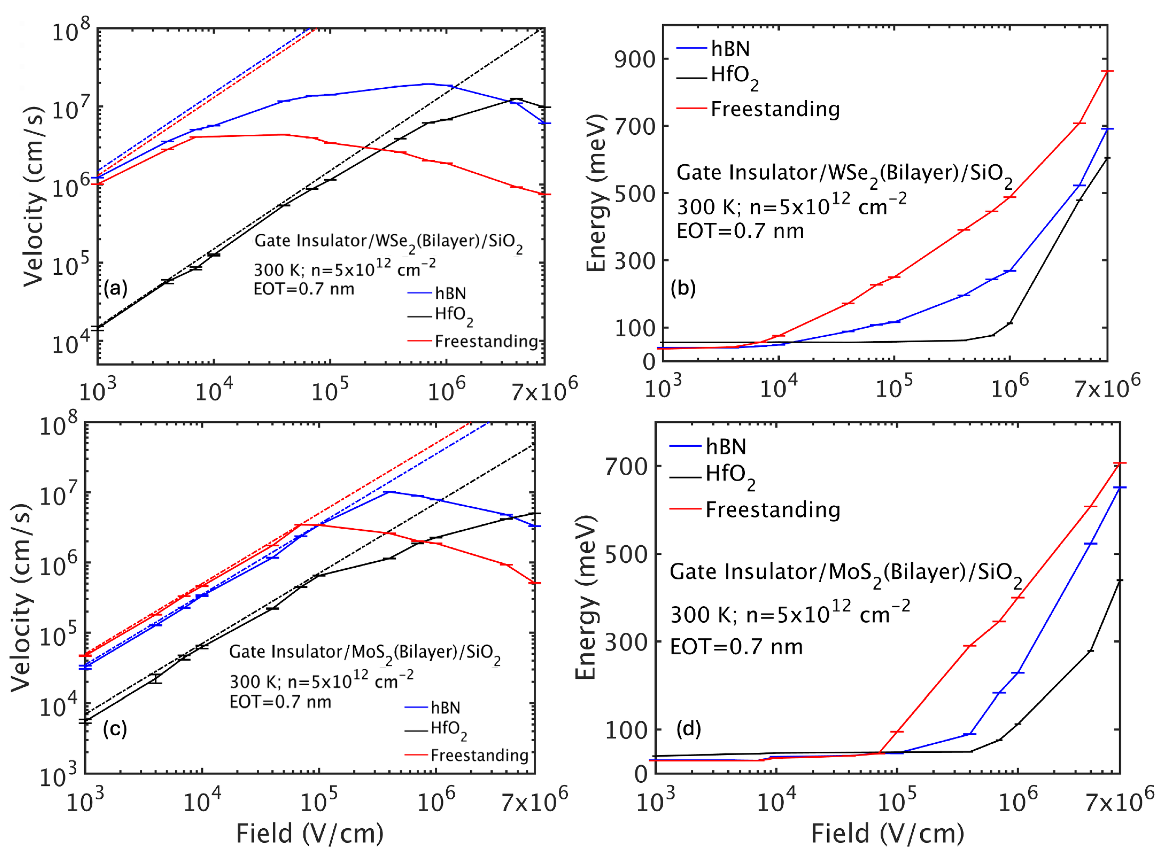
Figure 11.
Transfer characteristics (–) on linear and logarithmic scale (a) and the corresponding transconductance (b) for the HfO2/bilayer WSe2/SiO2 device ( nm, nm).
Figure 11.
Transfer characteristics (–) on linear and logarithmic scale (a) and the corresponding transconductance (b) for the HfO2/bilayer WSe2/SiO2 device ( nm, nm).
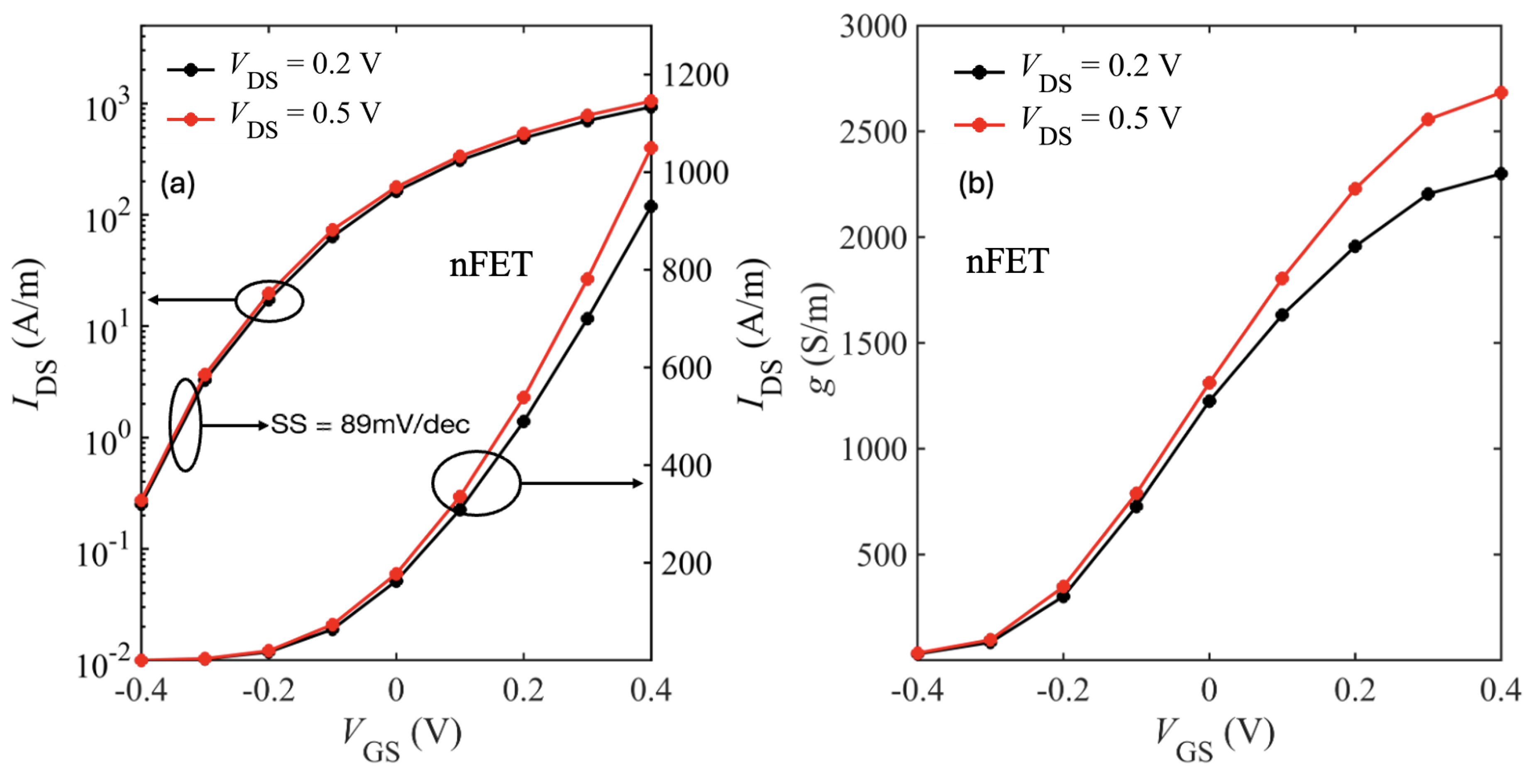
Figure 12.
(a) Channel potential energy and (b) average electron kinetic energy for different at V for the HfO2/bilayer WSe2/SiO2 device.
Figure 12.
(a) Channel potential energy and (b) average electron kinetic energy for different at V for the HfO2/bilayer WSe2/SiO2 device.
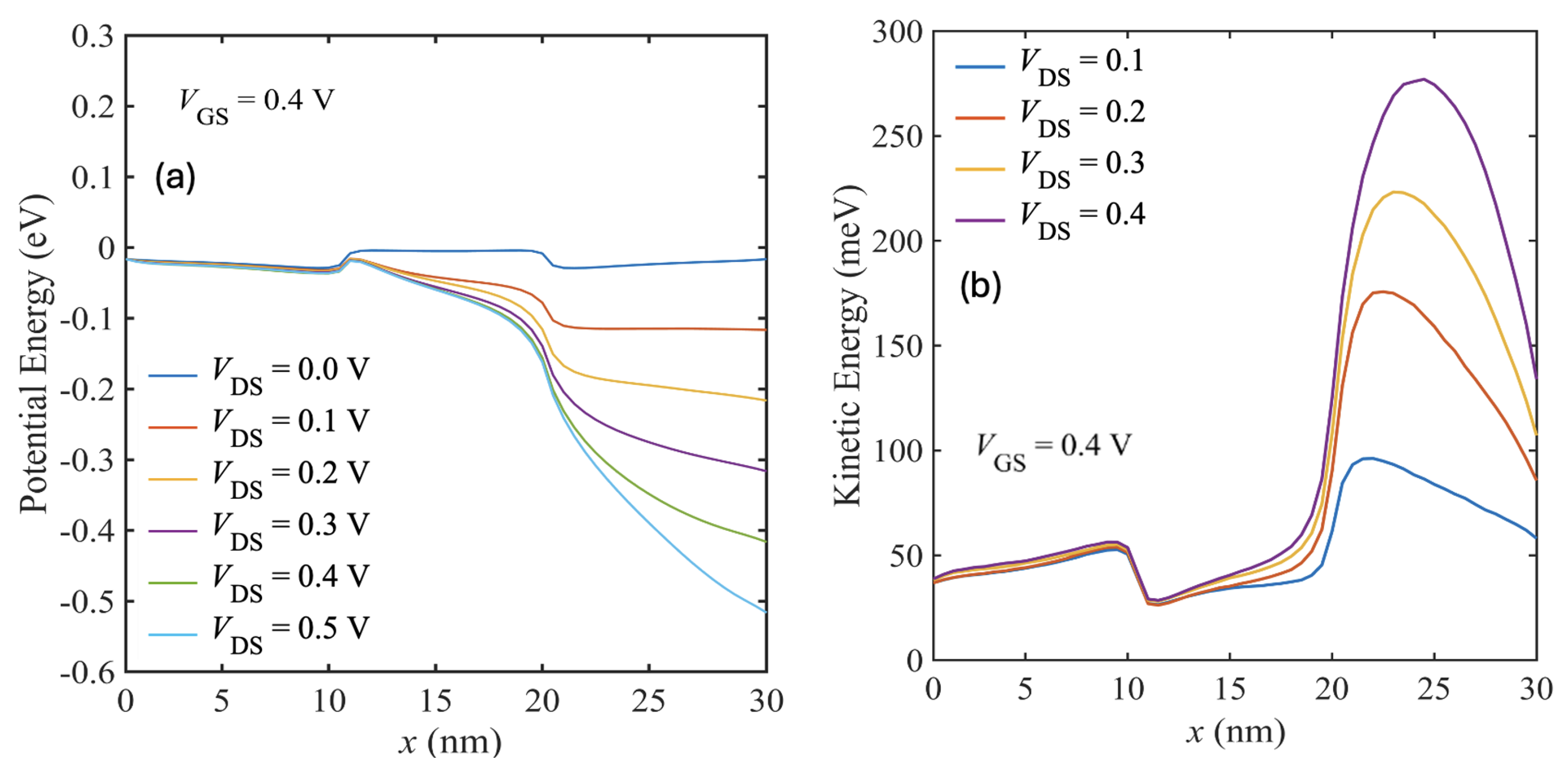
Figure 13.
Cross-section of the modified double-gate bilayer WSe2 MOSFET with SiO2 spacers and a 30 nm drain extension.
Figure 13.
Cross-section of the modified double-gate bilayer WSe2 MOSFET with SiO2 spacers and a 30 nm drain extension.
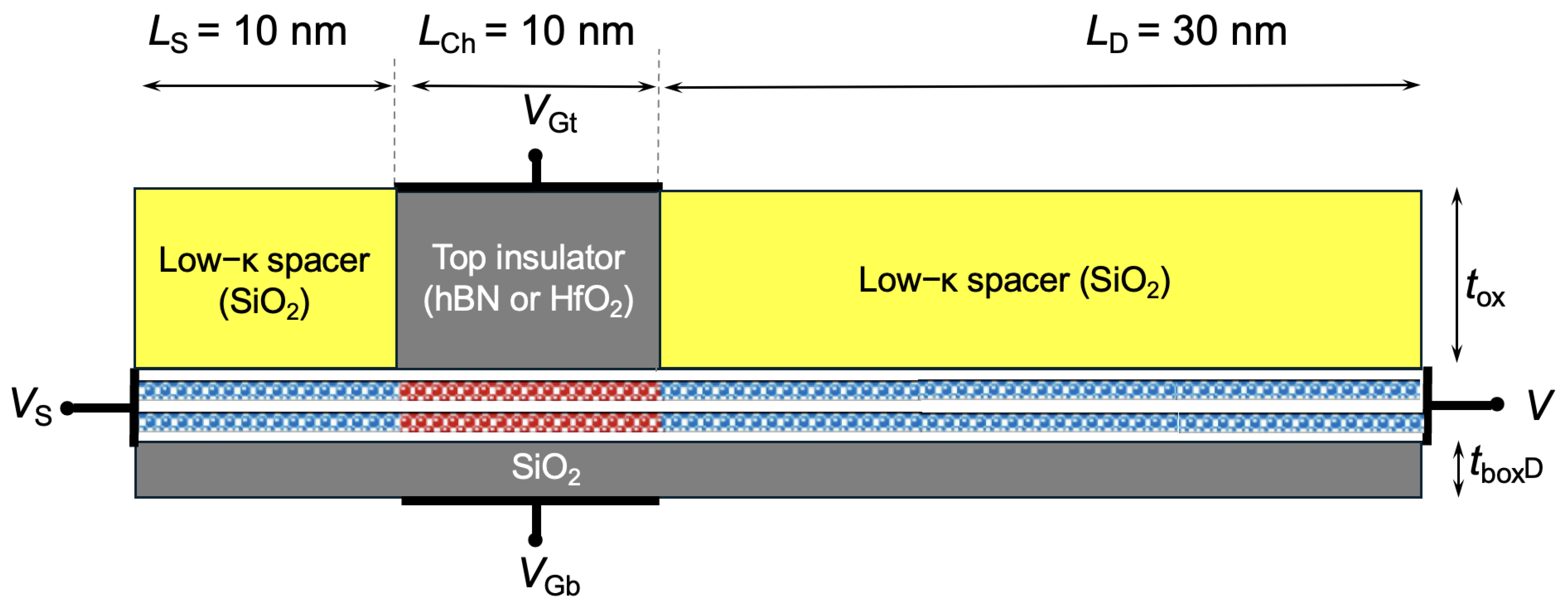
Figure 14.
Transfer characteristics (–) (a) and transconductance (b) for the SiO2-HfO2-SiO2/bilayer WSe2/SiO2 device device (30 nm drain extension).
Figure 14.
Transfer characteristics (–) (a) and transconductance (b) for the SiO2-HfO2-SiO2/bilayer WSe2/SiO2 device device (30 nm drain extension).
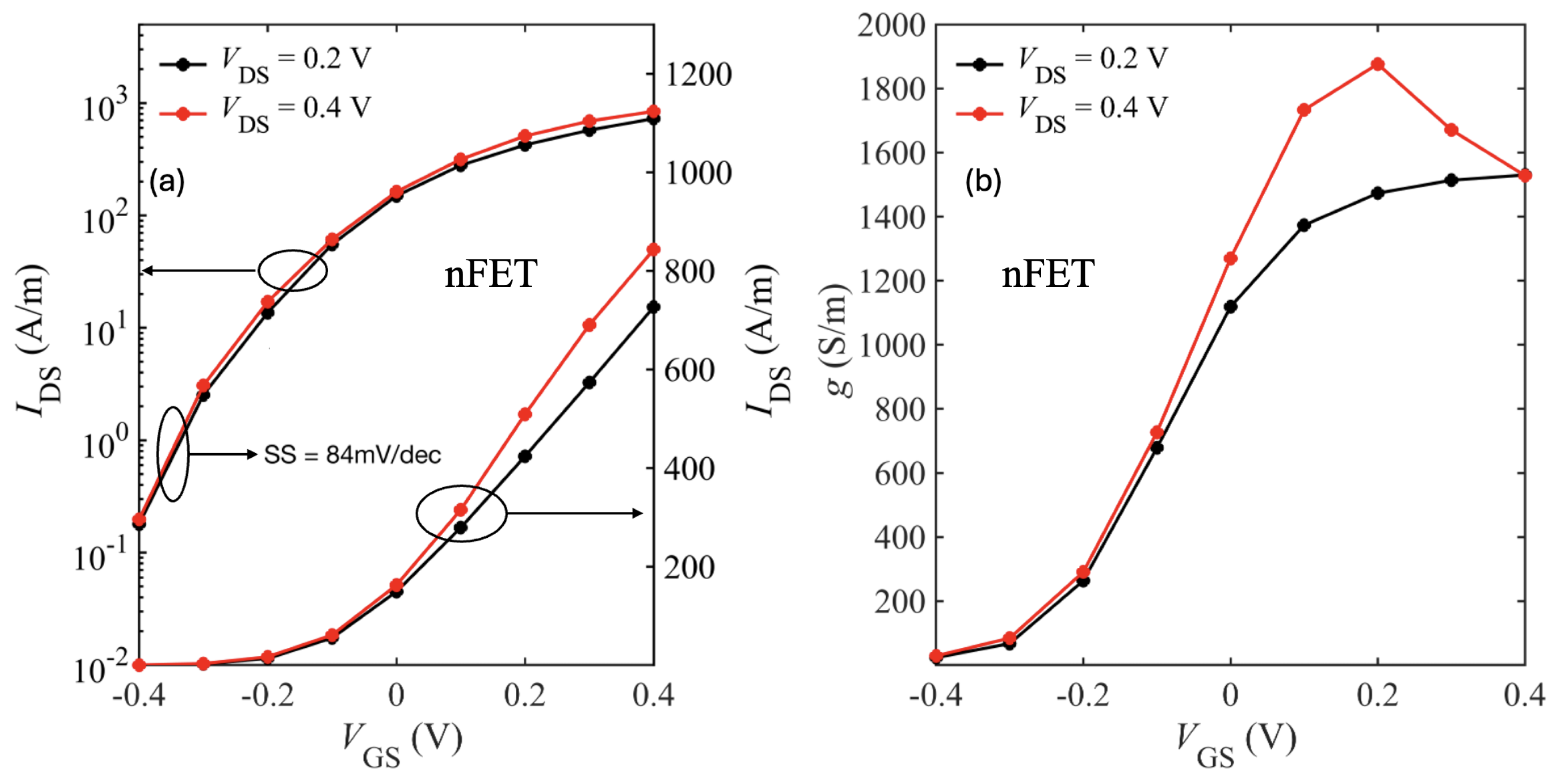
Figure 15.
Transfer characteristics (–) nFET (a) and pFET (b) for the SiO2-HfO2-SiO2/bilayer WSe2/SiO2 device device (30 nm drain extension).
Figure 15.
Transfer characteristics (–) nFET (a) and pFET (b) for the SiO2-HfO2-SiO2/bilayer WSe2/SiO2 device device (30 nm drain extension).
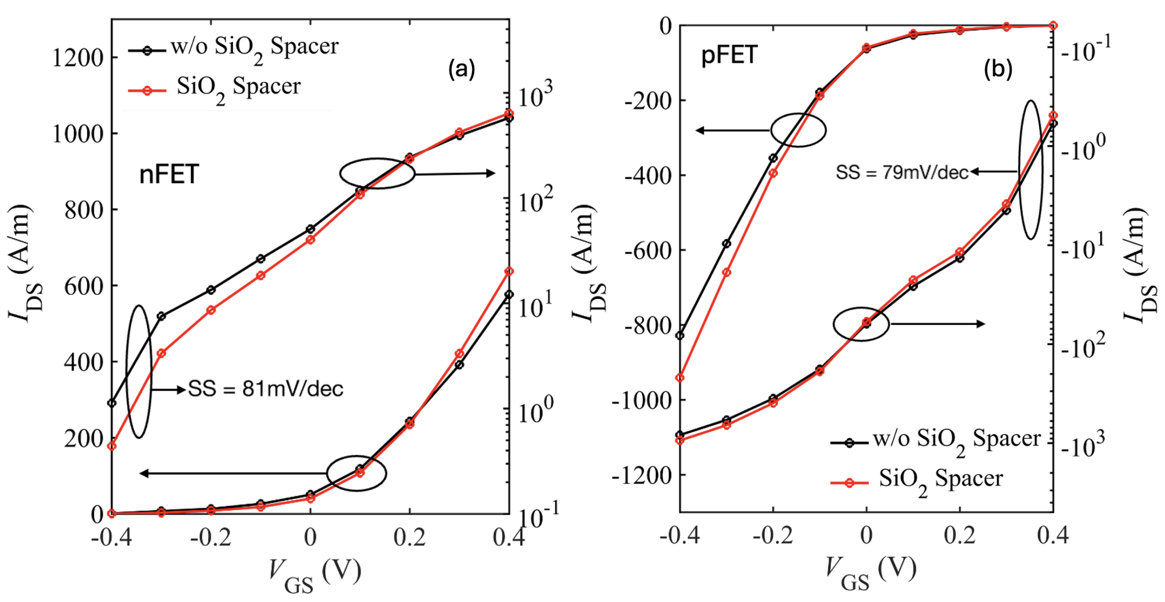
Figure 16.
Compact double-gate bilayer WSe2 device with 5 nm source/drain extensions.
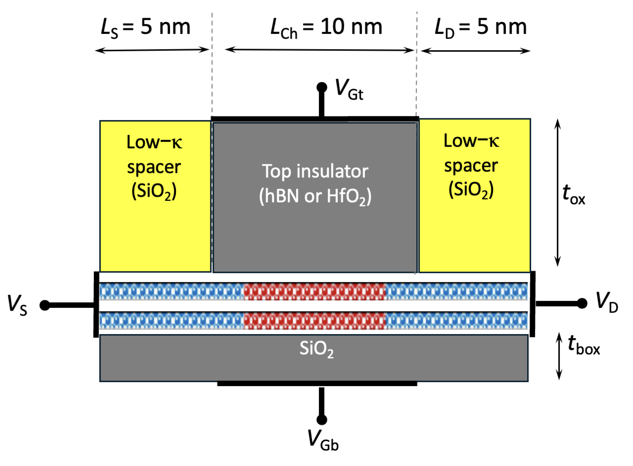
Figure 17.
Transfer characteristics (–) on linear and logarithmic scale and the corresponding transconductance for the 5nm S/D SiO2-HfO2-SiO2/bilayer WSe2/SiO2 nFET ((a) and (b)) and pFET ((c) and (d))
Figure 17.
Transfer characteristics (–) on linear and logarithmic scale and the corresponding transconductance for the 5nm S/D SiO2-HfO2-SiO2/bilayer WSe2/SiO2 nFET ((a) and (b)) and pFET ((c) and (d))
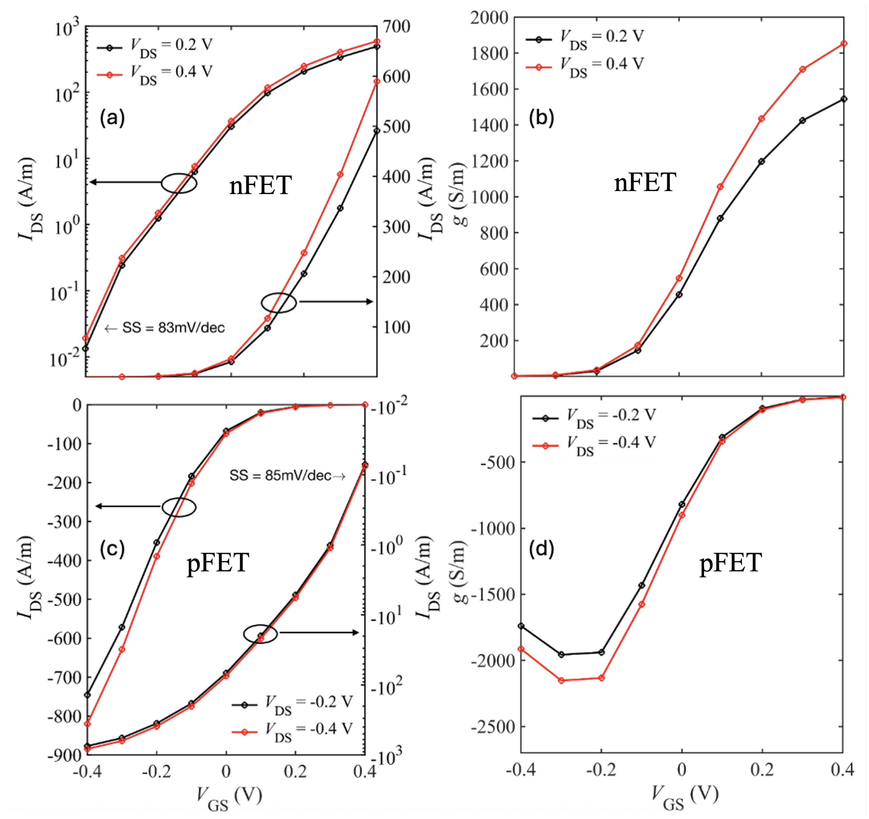
Figure 18.
Transfer characteristics (–) on linear and logarithmic scale and the corresponding transconductance for the 5nm S/D SiO2-hBN-SiO2/bilayer WSe2/SiO2 nFET ((a) and (b)) and pFET ((c) and (d))
Figure 18.
Transfer characteristics (–) on linear and logarithmic scale and the corresponding transconductance for the 5nm S/D SiO2-hBN-SiO2/bilayer WSe2/SiO2 nFET ((a) and (b)) and pFET ((c) and (d))
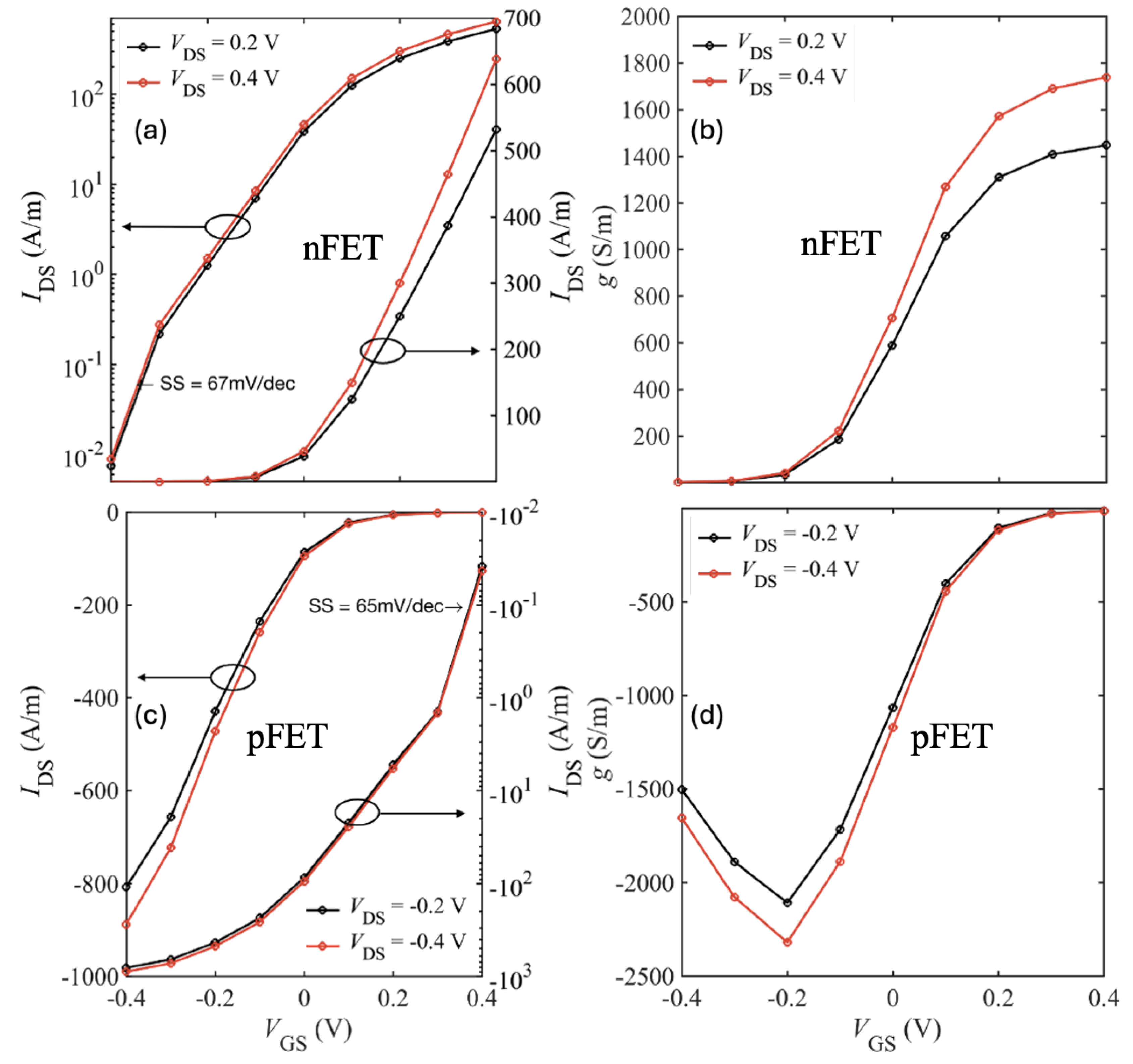
Figure 19.
The transfer characteristics ( vs. ) for the SiO2- HfO2-SiO2/bilayer-WSe2/SiO2 pFET with 5nm S/D extentions, plotted on linear and log scale
Figure 19.
The transfer characteristics ( vs. ) for the SiO2- HfO2-SiO2/bilayer-WSe2/SiO2 pFET with 5nm S/D extentions, plotted on linear and log scale
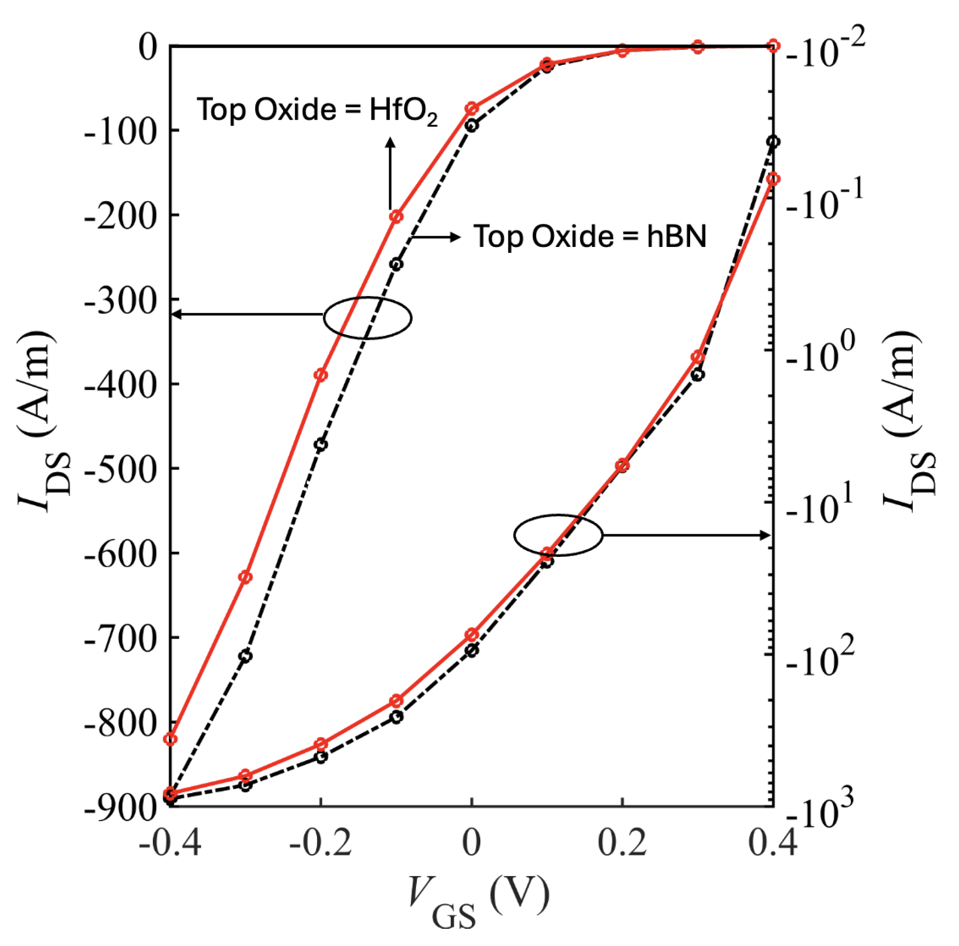

Table 1.
Quantum ESPRESSO computational parameters for bilayer TMD calculations.
| Parameter | Value |
|---|---|
| Kinetic energy cutoff | 60 Ry |
| Ionic minimization threshold | Ry |
| Self-consistent field threshold | Ry |
| Charge density cutoff | 240 Ry |
| k-point mesh | |
| q-point mesh |
Table 2.
Calculated hole mobility (cm2V−1s−1) for different configurations at 300 K.
| Material | Freestanding | hBN/TMD/SiO2 | HfO2/TMD/SiO2 |
|---|---|---|---|
| Bilayer WS2 | 2300 | 1530 | 100 |
| Bilayer WSe2 | 1300 | 1500 | 13 |
| Bilayer MoS2 | 50 | 35 | 7 |
| Monolayer WS2 | 750 | 1500 | 70 |
Table 3.
Calculated electron mobility (cm2V−1s−1) for different configurations at 300 K.
| Material | Freestanding | hBN/TMD/SiO2 | HfO2/TMD/SiO2 |
|---|---|---|---|
| Bilayer WS2 | 161 | 172 | 30 |
| Bilayer WSe2 | 201 | 163 | 36 |
| Bilayer MoS2 | 400 | 340 | 63 |
| Monolayer WS2 | 170 | 152 | 20 |
Table 4.
ON-current () in SiO2–HfO2–SiO2/bilayer-WSe2/SiO2 pFETs for different drain lengths and scattering mechanisms.
Table 4.
ON-current () in SiO2–HfO2–SiO2/bilayer-WSe2/SiO2 pFETs for different drain lengths and scattering mechanisms.
| Bias condition | Bulk phonons (30 nm drain) | Bulk phonons + IPP (30 nm drain) | Bulk phonons + IPP + Impurity (30 nm drain) | Bulk phonons + IPP + Impurity (5 nm drain) |
|---|---|---|---|---|
| V; V | 740 A/m | 660 A/m | 216 A/m | 630 A/m |
| V; V | 950 A/m | 870 A/m | 283 A/m | 820 A/m |
Table 5.
Performance metrics for short-drain WSe2 devices ( V).
| Device | (A/m) | (S/m) | SS (mV/dec) |
|---|---|---|---|
| nFET, HfO2 | 590 | 1850 | 83 |
| nFET, hBN | 640 | 1750 | 67 |
| pFET, HfO2 | 820 | 2200 | 85 |
| pFET, hBN | 890 | 2400 | 65 |
Table 6.
Performance metrics for short-drain WS2 devices ( V).
| Device | (A/m) | (S/m) | SS (mV/dec) |
|---|---|---|---|
| nFET, HfO2 | 330 | 980 | 90 |
| nFET, hBN | 390 | 1050 | 73 |
| pFET, HfO2 | 800 | 2500 | 89 |
| pFET, hBN | 870 | 2400 | 70 |
Disclaimer/Publisher’s Note: The statements, opinions and data contained in all publications are solely those of the individual author(s) and contributor(s) and not of MDPI and/or the editor(s). MDPI and/or the editor(s) disclaim responsibility for any injury to people or property resulting from any ideas, methods, instructions or products referred to in the content. |
© 2025 by the authors. Licensee MDPI, Basel, Switzerland. This article is an open access article distributed under the terms and conditions of the Creative Commons Attribution (CC BY) license (http://creativecommons.org/licenses/by/4.0/).
Copyright: This open access article is published under a Creative Commons CC BY 4.0 license, which permit the free download, distribution, and reuse, provided that the author and preprint are cited in any reuse.


