Submitted:
26 August 2025
Posted:
27 August 2025
You are already at the latest version
Abstract
Gallium-based liquid metal is corrosive to steel alloys, forming FeGa3 surface film, which can potentially be applied as a solid lubricant for enhancing wear resistance and mitigating liquid metal-induced corrosion. However, the characteristics of the surface film remain insufficiently explored. In this study, a liquid metal of Ga-In-Sn was ultrasonically soldered onto annealed or decarburised SKD11, then heated in a vacuum chamber to form a 30 μm-thick FeGa3 reaction layer. The surface film on the annealed specimen with alpha-ferrite microstructure exhibits high porosity with a surface roughness of 1.97 Ra. In contrast, the film on the decarburised specimen with ferritic microstructure showed minimal porosity with a surface roughness of 1.29 Ra. Nanoindentation tests showed that the surface films on annealed and decarburised substrates had Young’s Modulus of 231 GPa and 242 GPa, and nanohardness values of 11.4 GPa and 12.7 GPa, respectively. The high porosity is attributed to the suppression of FeGa3 formation in regions containing chromium carbides. Shear stress for fracture was measured using microcantilever tests at the interface between the substrate and inner matrix of the surface films, revealing lower fracture shear stress in the annealed specimen, attributed to the presence of larger pores within its microstructure.
Keywords:
surface film
; FeGa3
; SKD11
; micro-cantilever
; mechanical properties
; microstructure
1. Introduction
Gallium-based liquid metals (GBLMs), which consist of more than 60 mass% gallium, are gaining attention for their unique combination of properties. These include remarkably low melting points as low as -19°C, low toxicity, excellent electrical/thermal conductivity, high-temperature stability, and effective lubricity, even under demanding conditions. Consequently, GBLMs find applications in diverse fields such as flexible electronics, biomedical devices, advanced sensors, nuclear reactor cooling, and aerospace thermal management [1,2,3]. While variants like Galinstan (Ga-In-Sn) have shown promise as lubricants in extreme environments [4], their interaction with common structural materials like steel presents challenges. GBLM can be corrosive, directly alloying with the substrate and leading to the formation of an intermetallic surface film, predominantly FeGa3, on steel surfaces [5,6]. This FeGa3 compound, possessing a tetragonal P42/mnm crystal structure, exhibits intriguing characteristic such as high hardness and a high melting point [2,7]. Notably, FeGa3 film bonds strongly to the substrate [2], potentially offer self-lubricating properties under dry sliding condition [8], and, importantly, has been reported to inhibit further liquid metal (LM) corrosion on the steel substrate [5].
Prior works indicated that high chromium content, as found in stainless steel, can enhance resistance to LM corrosion [9]. This observation directs attention towards other high-chromium steel alloys like SKD11 tool steel, which contains over 12 mass%. Cr and features a microstructure reinforced by platelet chromium carbides for strength [10]. While Cr-C films have shown GBLM resistance [11], and the base SKD11 composition suggest potential compatibility, no recorded studies have investigated the specific interaction between SKD11 and GBLM or characterised the resulting surface film. Furthermore, understanding the influence of microstructural features, particularly the presence or absence of large chromium carbides on the formation of FeGa3 surface films has not been systematically investigated.
Understanding the nature of the FeGa3 surface film such as morphology, composition and thickness, formed on different substrates is critical for if it is intended to be used as a LM corrosion protection barrier. Geddis et al. [12] observed good corrosion resistance for SS304L and SS316L to GBLM up to 200°C, however, it was reported that thick and porous compound layers which consist of FeGa3 and CrGa4 were formed when these stainless steel alloys were exposed to GBLM at 300-400°C. Shin et al. [13] has proposed a model on liquid metal corrosion on austenitic stainless steel, which highlighted the influence of the substrate on the formation of the surface film. These findings underscore the sensitivity of the reaction layer’s microstructure to processing parameters and substrate chemistry. Factors inherent to SKD11, such as its high chromium content and the presence of distinct chromium carbides, could potentially influence kinetics and the development of microstructural features like porosity, even under different thermal conditions than those previous studies. The formation of such porosity is a critical concern, as it can significantly degrade mechanical properties such as hardness and elastic modulus [14], moreover promote pathway for reaction between the corrosive medium and the substrate [15]. While the formation of FeGa3 on certain steels is documented, the detailed microstructure and mechanical behaviour of such film on high-Cr, carbide-containing steels like SKD11 remain ambiguous.
For any surface film intended for wear protection or functional use, elucidating its mechanical properties such as hardness (H), Young’s Modulus (E), Poisson’s ratio (ν), shear strength and fracture behaviour dictate performance [16,17,18]. Desirable characteristic often includes a high H/E surface film ratio and the value of the surface film’s Young’s Modulus to closely match to the substrates to ensure mechanical compatibility and durability. Guo et al. [2] examined FeGa3 surface film formed on T91 steel using Galinstan, reporting an average layer thickness of 26.8 μm with irregular, loose grains less than 5 μm in size. The nano-indentation hardness (H) and reduced modulus (Er) of the film were measured to be 7.63 GPa and 241 GPa, respectively, close to the substrate modulus of 275 GPa. However, the inherent brittleness of the FeGa3 intermetallic compound, attributed to insufficient slip systems[19] poses challenges for wear application. Buckley and Johnson [8] highlighted the importance of shear strength and film adhesion to the substrate during sliding, as excessive shearing can exacerbate substrate reaction.
Accurate mechanical characterisation of thin, brittle film like FeGa3 present significant challenges due to the small length scale involved and the potential influence of the underlaying substrate [20,21], especially when microstructural defects like porosity are present. Scratch testing is commonly used to asses adhesion of film to the substrate [2,22], while nanoindentation tests is a widely adopted for evaluating the hardness and Young’s modulus of thin films due to its localised nature and relatively simple sample preparation [23]. Depending on the type of surface film, the nanoindentation test is not enough to understand its mechanical property due to the fact that the mechanical response under compressive and tensile stresses are different, especially for brittle surface films [24]. One of the methods that has been utilised to measure the mechanical response for tensile conditions is obtained with a micro sized cantilever fabricated by using a focus ion beam (FIB) [25,26,27]. The free end of the microcantilever beam is loaded using a nanoindenter, where the load displacement curve is obtained [20,24]. For example, Yamaguchi et al. successfully applied this method to characterise thin, brittle BaTiO3 film [24].
In the present study, we apply this combined methodology to evaluate the microstructure and mechanical properties of the surface film formed on SKD11 with and without the large chromium carbide precipitates. Nanoindentation tests and microcantilever shear tests were performed to investigate the mechanical properties of the surface film. The intrinsic porosity of the surface films was evaluated by binarizing the SEM image. The effects of chromium carbides and porosity on the mechanical properties of the FeGa3 were also investigated.
2. Materials and Methods
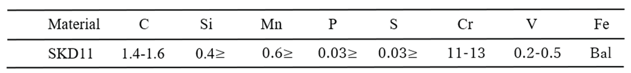
SKD11 was used for substrate, the chemical composition of which is shown in Table 1. Two types of substrates were prepared: an annealed SKD11 (Specimen A) and a surface-decarburised SKD11 (Specimen B). Heat diagrams are shown in Figure 1a,b for Specimen A and Specimen B, respectively. Specimen B was prepared to distinguish the effect of dissolving the large chromium carbide precipitates in the SKD11 substrate on the formation of the FeGa3 compound. The oxides scale which was produced during the decarburisation process were removed. The specimens surface were then mirror polished to 0.04≥Ra, then ultrasonically cleaned in acetone and ethanol and dried in air. Liquid Ga-In-Sn was then ultrasonically soldered (USM-560, Sunbonder) on both surfaces of Specimens A and B according to method by Auger et al. [28], then heated up in a vacuum chamber at 400°C for 5 hours to form FeGa3 reaction layers with the thickness of 30 μm. The surface roughness of the formed surface films is then measured using stylus profilometer (Surtronic S-100, Taylor Hobson).
The phase composition on the FeGa3 surface on both specimens were identified using X-ray diffraction (XRD, Smartlab, Rigaku), using Cu-Kα radiation over and angular angle of 15 to 80° with scan speed of 0.6° / min at 0.01° interval. This followed by analysis on the diffraction peak using PDXL2 analysis software. For microstructural analysis, the specimens were first cross sectioned, mounted on conductive resin and polished, involving the use of emery paper with grit size ranging from #320 to # 3000, followed by polishing with diamond slurry (grain size: 1 μm & 0.1 μm) and finally using 0.25 μm colloidal silica. Microstructural observations were conducted using a field-emission scanning electron microscope (FE-SEM, SU5000, HITACHI) with an accelerating voltage of 15 kV. The element mapping on the specimen’s cross section was conducted using energy dispersive spectroscopy (EDS, HITS4300SE, EDAX) with an accelerating voltage of 25 kV.
Microcantilever beam specimens were fabricated using focus ion beam technique (FIB-SEM, Quanta 3D 200i, ThermoFisher Scientific) on the cross-sectioned of FeGa3 layer of both specimens at the interface between the respective surface film and the substrate, as well as at the centre of the surface film. Acceleration voltage of 30 kV and current of 15 nA were used to produce the microcantilever with dimension as shown in Figure 2a.
Nanoindentation tests were carried out (ENT-1100, Elionix) to investigate the nanohardness and elastic modulus of the FeGa3 layer as well as the substrate with the load from 0.25 mN to 10mN for the FeGa3 layer and 5 mN for the substrate, respectively. Shear tests on the microcantilever beam were conducted using a nanoindenter (ENT-5, Elionix) with a flat-punch indentation tip, where the whole cantilever beam’s surface was pressed, with a displacement speed of 15 nm/sec, the schematic of which is shown in Figure 2b. The shear stress at the notch root was estimated using Equation (1), where τ is the shear stress, F is the load at failure, and A is the cross-sectional area of the microcantilever beam [24].
The porosity of the FeGa3 surface film for both Specimen A and B were measured using digital image analysis (DIA) on the SEM image for both specimens, using the open code program ImageJ [29]. The porous area was taken as percentage from the total area for each measured location, where the average percentage were then calculated. At least five areas were taken for each specimen on the FeGa3 surface film.
3. Results
3.1. Microstructure
Figure 3a,b show SEM images of the top surfaces for Specimen A and B after the heat treatment, respectively. Figure 3a shows that Specimen A exhibits a surface primarily composed of irregular, loose packed grains as indicated by the red arrow. Scattered across this granular matrix are distinct, smooth islands of irregular size and shape as indicated by the white arrow in the figure. In contrast, Figure 3b shows that Specimen B also displays a matrix of irregular, loosely packed grains, however, it also shows that small pores are distributed across the surface, and scattered polygonal structures of various sizes as indicated by the white arrow in the figure. Quantitative surface roughness measurement using a stylus profilometer showed a value of 1.97 Ra and 1.29 Ra for Specimen A and Specimen B, respectively, indicating smoother surface topography for Specimen B at the micrometre scale.
Figure 3c,d shows XRD profiles taken from the top surface of Specimens A and B. They show matching peaks with the standard card #00-44-0824, indicating that FeGa3 is the dominant phase formed by the reaction of Fe and liquid Ga-In-Sn. Figure 3e shows the enlarged area surrounded by a red rectangle in Figure 3c,d, which shows the highest intensity peak for FeGa3 located at (2 1 2). Peak broadening is seen in both specimens, which gives the full-width half-maximum (FWHM) value of 0.11 and 0.20, for Specimen A and B, respectively. This broadening suggests the presence of nanocrystalline or submicron grains within the FeGa3 phase for both specimens. According to Scherrer relationship [30], the smaller FWHM of 0.11 for Specimen A suggest potentially larger average crystallite sizes compared to Specimen B of 0.20 [31]. Furthermore, this broadening is presumed to be influenced by the presence of residual strain in the FeGa3 grain for both specimens. Depending on whether the residual stress is compressive or tensile, this will have a significant effect on the potential application of the surface film [32].
Figure 3c also shows the peaks associated with chromium compound labelled by the triangle symbol, matching with those in the standard PDF card #01-71-3789 and #00-46-1034, indicating the presence of the Cr7C3 and CrGa4 compounds in the surface film. It is to be stressed that In-Sn compounds are detected at major peaks of PDF card #01-073-9034 for Specimen A, however, are less detected for Specimen B, marked by the circular symbol in Figure 3c,d. This suggests substantial segregation and solidification of distinct In-Sn phase in Specimen A, whereas in Specimen B, these elements are presumed to be incorporated into the FeGa3 lattice, exist below the XRD detection limit, or are segregated in a different manner.
Figure 4a,b show SEM images of the cross-sections near the top surfaces of Specimens A and B, respectively. Figure 4a shows that the FeGa3 surface film on Specimen A has a thickness of 30 ±5 μm with many numbers of macropores, indicated by the red arrows. The substantial internal porosity throughout the layer thickness is estimated to be 8.4±5.2% by image binarisation. Figure 4c shows an enlarged image from the area indicated by the blue rectangle in Figure 4a, where fine chromium carbides are embedded in the FeGa3 layer (indicated by white arrow in Figure 4c), which originated from the SKD11 substrate, as seen in SEM image of the interface between the FeGa3 layer and the SKD11 substrate in Figure 4e. The pores, indicated by the red arrow, formed in the vicinity of chromium carbide as shown in Figure 4c. The carbides also lead to an inhomogeneous corrosion rate which results in the rough interface between the surface film and substrate, as indicated by the difference in depth between the highest peak and lowest depth indicated by the blue arrows in Figure 4a where the difference can be seen at the position of large carbide particles in the SKD11 matrix. Large size of Cr7C3 and smaller size of M23C6 have been distributed in the matrix of SKD11 [10], as indicated by the white arrows in Figure 4a,e.
Figure 4b shows the cross section of Specimen B, indicating significantly fewer internal pores and a much denser FeGa3 layer with a thickness of 30 ± 3 μm. The distribution of pores is not uniform. The porosities as indicated by the red arrows in Figure 4f, 3 μm beneath the top surface is estimated to be 10.8±1.8% by image binarization. From this depth onwards toward the interface of the substrate, the porosity is estimated to be 0.2±0.1%. Throughout the layer, the average porosity is estimated to be 1.14±0.2%. A small number and size of carbide particles are embedded in the FeGa3 layer, as indicated by the black arrows in Figure 4b. Consistent with XRD findings, polygonal-shaped crystals considered as CrGa4 detected at peaks of 31.77°, 39.26°, 39.76° and 45.72° in a XRD profile as shown in Figure 3c with standard card #00-046-1034 are observed on the outer surface of the FeGa3 layer, where the enlarged image of the crystal structure can be seen in Figure 4f.
As a result of Cr7C3 extinction due to decarburization, a flat interface between the FeGa3 layer and the substrate SKD11 was obtained in Specimen B, as shown in Figure 4b. Meanwhile, the decarburised SKD11 substrate has a larger grain size as a result of the decarburisation process compared to the substrate of Specimen A. In addition to that, large size of chromium carbides had dissolved in the substrate near the interface.
The FeGa3 matrixes in both Specimens A and B consist of irregularly shaped, sub-micron grains with an approximate circle average diameter (CAD) of 0.2μm, as shown in the BSE image in Figure 4c and 4d. Given that FeGa3 is the primary composition of the surface film, these grains are reasonably assumed to be FeGa3. Contrary to previous finding [2], the grain size of the FeGa3 appears significantly smaller. However, this observation aligns with reports of nano-sized FeGa3 grains in other literature [4].
Figure 5 shows EDS maps of the cross-section of Specimen A, indicating the existence of both Fe and Ga in the FeGa3 layer as the layer is mainly of FeGa3 compound. High concentration of Cr in place, as shown by the red arrow in Figure 5c, correlating with the detection of chromium carbide in the FeGa3 compound for Specimen A determined with using XRD. It is presumed that pores near the area where Cr concentrates are the place where chromium carbide had existed, as indicated by the red arrow in Figure 5a. Notably, In and Sn signals in Figure 5e and 5f, respectively, are also concentrated in these Cr-rich regions, often adjacent to pores, as shown in Figure 5a. This co-localisation suggests that the observed porosity is associated with the prior presence of the In-Sn phase, which preferentially segregates near the embedded chromium carbides. Features resembling the smooth island in Figure 3a are also observed within the cross-section, rich in In and Sn as indicated by the white arrows in Figure 5a,e,f.
Figure 6 shows EDS maps on the cross-section of Specimen B, showing similar detection for Fe and Ga as shown in Figure 5, which is attributed to the FeGa3 compound. The small particles are conceded to be M23C6 due to the size and the high concentration of Cr, as indicated by the red arrows in Figure 6a,c. The high concentration of Cr and Ga near the surface, as indicated by the white arrows in Figure 6a,c,d corresponds to the precipitates shown in Figure 4f. It is considered to be CrGa4 as reported by Yu et al. [33] when stainless steels were corroded with gallium-based liquid metals at high temperatures.
3.2. Mechanical Test
In order to reveal the mechanical properties of FeGa3, a series of nanoindentation tests were conducted. These tests aimed to determine the nanohardness and Young’s modulus as a function of applied load, investigate the property across the film-substrate interface, and estimate the effective bulk mechanical properties by accounting for film porosity. Figure 7a shows the average nanohardness (HIT) for Specimen A and B, measured at the centre of their surface films. HIT generally decreases as the load increases from 0.25 mN to 10 mN in both specimens. Specimen A yielded an average HIT of 13.5±1.4 GPa at 0.25 mN, appeared to stabilise around 11.4 ±1.7 GPa at 1mN, and subsequently decreased to 7.8±2.3 GPa at 10mN. Specimen B demonstrated a comparable pattern, although with generally higher HIT compared to Specimen A. Its HIT was 16.1±2.7 GPa at 0.25 mN, decreased to 12.7±1.5 GPa at 1 mN, and then appeared to reach more stable value of approximately 11 GPa at 5 mN and 10 mN.
Figure 7b presents the average Young’s Modulus (EIT) for Specimens A and B. Similar to HIT, EIT decreased as the load increased from 0.25 mN to 10 mN. For Specimen A, EIT was at 258.1 ± 24.7 GPa at 0.25mN, and decreased to 231.7 ±19.0 GPa at 1mN, and further reduced to 188.9 ± 26.5 GPa at 10mN load. Specimen B showed a higher average value compared to Specimen A with a consistent decline towards higher load. EIT value for Specimen B was 277.1±47.3 GPa at 0.25 mN, dropping to 242.4±26.5 GPa at 1mN load, and stabilised to 220.4±6.2 GPa at 10mN.
The large standard deviation, especially at lower loads, should reflect the influence of local microstructure such as crystallographic orientation, number of grains involved, and grain boundaries [34]. To verify the above, the projected contact area was firstly calculated, (Ac). The commonly used equations in nanoindentation of H = P / Ac was used to obtain the Ac, where H is the indentation hardness obtained from the nanoindentation test and P as the applied load [35]. The calculated Ac based on applied load and indentation hardness is shown in Figure 7c. At indentation load of 1mN, the Ac was approximately 0.087 μm2 for Specimen A and 0.081 μm2 for Specimen B. Based on the relationship between indentation depth (hc) and projected contact area, Ac=24.504hc2 [36], this yield hc to be approximately 59 nm for Specimen A and 57 nm for Specimen B. The characteristic lateral dimension of a Berkovich indent is approximately 7.5 x hc [36]. Thus, at 1mN, the indent size is approximately 0.44 μm at lateral side length. Comparing this indent dimension with the average grain size of Specimens A and B, it is evident that indentation at 1mN interacts with a few grains as indicated by the indent mark denoted by the blue arrow in Figure 4c and 4d. As the load further increased beyond 1mN, Ac exponentially increased, as depicted in Figure 7c. It is due to cracking of from the nanoindents, where the value of HIT does not show the actual value. Consequently, 1mN load was selected as reference load for further indentation tests across the surface film.
The values of HIT were measured across the cross-section. Loads of 1 mN and 5 mN were applied to the compound layer and the substrate, respectively. Figure 7d shows the average value of HIT, indicating that HIT varies across the surface layer while it is nearly constant in the matrix. The lowest hardness inside the compound layer of Specimen A was recorded near the top surface of 8.5 ± 3.3 GPa, while the hardness at the centre of the compound layer is 11 ± 2 GPa . Overall, the HIT of the compound is more than 3 times higher than that of the substrate of 3 ± 0.8 GPa. Meanwhile, the compound layer of Specimen B also shows lower HIT at the top surface of 9 ± 1.7GPa, however, a more consistent reading at the centre of the compound of 13 ±1.5 GPa. The HIT on the substrate exhibited 2 ± 0.13 GPa. HIT of the compound is of approximately 6 times higher than of the substrate.
Figure 7e shows EIT across the cross-section, the value of which is taken simultaneously with HIT, showing the same trend with EIT. The lowest value of Specimen A was found to be near the top surface of 179 ± 0.13GPa while the value fluctuates toward the centre with an average of 232 ± 19 GPa. The average value of EIT for the substrate was 266 ± 19 GPa, which is slightly higher than that for the compound layer. EIT of the compound layer for Specimen B is more consistent across the compound layer and close to the value of the substrate. The average values of EIT for the compound layer and the substrate are 242 ± 27 GPa and 243 ±15 GPa, respectively, although slight reduction in EIT can be observed at the top surface of the surface film of 203 ± 37 GPa.
To validate the EIT value obtained from the nanoindentation test, the EIT was compared with that retrieved from the Materials Project for Ga3Fe (mp-636368) from database version v2023.11.1. Here, the value of Poisson ratio, v, and the bulk modulus, K, for FeGa3 were reported to be 0.23 and 101 GPa, respectively [37]. The Young’s modulus obtained with the equation of E = 3K(1-2v) [38] was estimated to be 168 GPa. The reference value has good agreement with results from Specimen A at higher load but is significantly much lower compared to results from Specimen B at all loads. Additionally, the inconsistency in the HIT and EIT value, especially for specimen A probed further investigation.
3.3. Microcantilever Test
Figure 8a and 8b show fabricated microcantilever beams for Specimens A and B, respectively, formed at the interface between the FeGa3 compound layer and the substrate before the shearing tests. White contrasts on the surface in Specimen A indicate the presence of chromium carbide precipitates embedded in the cantilever beam while Specimen B has a smoother surface, indicating a lower number of chromium carbide precipitates in the cantilever beam. Figure 8c and 8d show fracture surfaces of the microcantilever after shearing tests. The fracture surface of Specimen A is rough, showing intergranular failure and failure through a region with microstructural heterogeneity. On the other hand, the fracture surface of Specimen B, as shown in Figure 8d, was smoother with small number of macropores.
Figure 9a,b show fabricated microcantilever beams inside the compound layer for Specimens A and B before shearing tests, respectively. The cantilevers were fabricated at a minimum distance of 10 μm from the top surface of both specimens. The fracture surface of Specimen A in Figure 9c shows the existence of macropores and individual particle-like features, indicating the high porosity of the internal structure of the microcantilever beam as well as the existence of the chromium carbide particles (red arrows) in the inner matrix of Specimen A. Fracture has likely propagated through the interconnected pores and along the weakly bonded chromium carbide particles interfaces. On the other hand, the microcantilever beam of Specimen B itself did not fracture although the crack propagated from the porous top surface, as shown in Figure 9d. This indicates that the compound itself in Specimen B is much more resistance to fracture compared to that of Specimen A.
Figure 10a shows the load-displacement curves obtained from bending tests with the cantilever at the interface. The red curve is for Specimen A, exhibiting a maximum load of around 6 mN at a displacement of 0.26 μm, corresponding to a calculated shear stress of 239 MPa, where the cross-sectional area of the cantilever is 2.4 × 10⁻⁵ mm2. The black curve is for Specimen B, showing a much steeper initial slope, indicating higher stiffness compared to Specimen A. The force increases almost linearly to much higher load leading to the fracture with the load of 68 mN. The shear stress at fracture is expected to be approximately 1814 MPa with the cross-section of cantilever of 3.7x10⁻⁵ mm2. The shear stress for the fracture of Specimen B is approximately 7.5 times higher than that of Specimen A. It is presumed that the Specimen B with low porosity show the true strength of the compound layer.
Figure 10b shows the force-displacement curves obtained from the cantilevers formed inside the compound layer. The red curve is from Specimen A, indicating that the Specimen A fractured at the load of 2.4 mN, which corresponds to 57 MPa. The black curve is from Specimen B, indicating that the microcantilever beam for Specimen B itself did not fracture completely; instead, cracks were initiated from the top surface as indicated by the white arrows in Figure 9d. This initiation of cracks leads to the sudden drop in load indicated by the black arrow in Figure 10b. Further applied shearing load until 50 mN on the microcantilever also did not fracture the cantilever. These results indicate that the compound layer in Specimen B has higher resistance to fracture than Specimen A.
4. Discussion
4.1. Microstructure and Mechanical Properties
It was indicated that overall porosity of FeGa3 surface film in Specimen A is higher and distributed throughout the compound layer. In contrast, the porosity of Specimen B is concentrated at the top surface and homogenous inside. It is because GBLM has low reaction and does not readily wet chromium carbide with higher chromium content [11]. The chromium carbide of SKD11 mainly consists of Cr7C3 and M23C6 with the chromium to carbon ratio of 7:3 and 8:2, respectively. Previous work by Lindersson [11] shows that GBLM does react with chromium carbide film of lower chromium content of Cr to C ratio of 3.7 : 6.3. At the same time, the solubility of Fe and Cr in liquid Ga at 400℃ follows the order of Fe > Cr [9]. Therefore, while the GBLM alloy reacts first with the Fe in the annealed base material to form the FeGa3 layer, the Cr rich carbide remains as it is. As the FeGa3 layer grows, the GBLM still does not readily wet the surface of the Cr rich carbide in the SKD11 interface. This makes the GBLM to react with the Fe near the Cr rich carbide surrounding. If another large particle of Cr rich carbide is present, as indicated by the red arrow in Figure 5a, this can lead to multiple pores, and as more Cr rich carbide particle present, a high-porosity layer is produced.
The decarburisation process of Specimen B was successful in dissolving the large primary chromium carbides and small secondary chromium carbides which were originally present in the base material. The dissolution of these Cr rich carbides dispersed the Cr element much evenly throughout the decarburised interface, as shown in Figure 6c. This resulted in the formation of more uniform FeGa3 at the interface between substrate of Specimen B and the compound layer, preventing the formation of large voids as seen in Specimen A. It is to be noted that exposure of the gallium-based liquid metal to a high chromium ferrous alloy at high temperature is still subject to corrosion, as reported in other studies [12]. The observation of CrGa4 on the surface of Specimen B align with such high-temperature reactions.
The differences in porosity and carbide distribution influence the mechanical properties. The compound layer in Specimen A with its higher porosity and embedded particles generally shows lower hardness, lower Young’s modulus and significantly lower shear strength compared to Specimen B. This suggests that the macroscopic elastic constant differed due to the existence of pores. Ternero et al. have shown that the porosity of 10% resulted in a decrease of 30 % in Young’s modulus [39]. The porosity of Specimen A was approximately 8.4 ± 5.2% throughout the surface film as mentioned in Figure 4a, which can be interpreted as the reduction of Young’s modulus due to the higher porosity. The smoother interface and denser compound layer at the centre of Specimen B contributed to its superior mechanical performance, including better matching of its Young’s modulus with the substrate.
4.2. Microcantilever Beam Shearing Test
The microcantilever shear test revealed the influence of porosity on the actual strength of the bulk FeGa3 compound. The porosities were caused by the excessive presence of chromium carbide particles, as discussed in the previous subsection. Although the values of Young’s modulus of FeGa3 obtained by nanoindentation tests were not much different between Specimens A and B, the slope of the load-displacement curve in Figure 10 is not identical. The change in slope corresponds to the change in shear modulus, as the simple shear tests were conducted using microcantilevers in this study. The difference in the slope indicates that the bulk shear modulus of Specimen B is higher than that of Specimen A. The slope is considered to be influenced mainly by the presence of inherent porosity. That is, the higher slope in Specimen B is due to the low porosity of 0.2% where the cantilever was formed. This trend was also observed in shear tests conducted within the inner surface compound layer, where Specimen A exhibited lower shear strength than Specimen B did. In Specimen B, crack propagation initiated at the top surface due to porosity, causing it to fail under lower shear loads, while the central region remains intact.
The friction-reducing [8] is attributed to the shearing of the FeGa3 surface film. As the surface film heats up, a thin lubricating film forms between the sliding surfaces. However, if the whole compound is sheared away, the protective layer is lost [5], exposing the substrate to further reaction with the liquid gallium. In the case of Specimen A, despite the FeGa3 compound’s high hardness and Young’s modulus, the lower shear strength of the surface film makes it more susceptible to shearing during sliding. While this may enhance friction and wear reduction, it is also increased the risk of substrate corrosion. In contrast, Specimen B demonstrated higher shear strength at both the interface and the centre of the surface film, with only the top surface showing lower shear resistance. As temperature rises, the sheared top surface contributes to friction and wear reduction, while the intact central region continues to protect the substrate from LM corrosion.
5. Conclusions
Mechanical properties of FeGa3 formed on SKD 11 was investigated. The following results were obtained.
- 1)
- The FeGa3 surface film on an annealed substrate exhibits high porosity due to the inability of the reaction between the gallium-based liquid metal and chromium carbide. On the other hand, the FeGa3 on decarburised SKD11 substrate showed less porosity due to the dissolution of the chromium carbide precipitates into the SKD11 matrix.
- 2)
- FeGa3 surface film on both substrates shows the nanohardness of approximately 11 – 13 GPa.
- 3)
- The decarburisation process significantly improved the shear strength of the compound layer. The compound layer on the decarburised substrate showed more than six times higher shear strength than that on the annealed substrate, indicating enhanced potential for practical applications under high mechanical stresses.
Author Contributions
Writing-original draft preparation, visualization, methodology, investigation, formal analysis, data curation, R.P.; supervision, writing – review and editing, M.T. (Masaki Tanaka); supervision, data curation, S.Y., T.M., K.Y.; validation, M.T. (Masahiko Tezuka), Y.Y. (Yasufumi Yoshida); investigation, formal analysis, Y.Y. (Yukinari Yoshida), M.H. All authors have read and agreed to the published version of the manuscript.
Funding
This study was financially supported by Canon Electron Tubes & Devices Co., Ltd.
Informed Consent Statement
Not applicable.
Data Availability Statement
The data presented in this study are available on request from the corresponding author.
Acknowledgments
The authors would like to thank Mz. Yuka Ashisada for her supports with experiments.
Conflicts of Interest
The authors Masahiko Tezuka, Yasufumi Yoshida, Yukinari Yoshida, and Makoto Higashionna are employees of Canon Electron Tube & Devices Co., Ltd. and contributed to the study as a co-author, including participation in technical support, discussions on study design, data interpretation, and reviewing the manuscript. The authors Roonie Protasius, Masaki Tanaka, Shigeto Yamasaki, Tatsuya Morikawa, and Kazuyuki Yagi declare that they have no conflicts of interest. The funder had no role in influencing the final interpretation of the results or the decision to publish.
References
- Handschuh-Wang, S.; Stadler, F.J.; Zhou, X. Critical Review on the Physical Properties of Gallium-Based Liquid Metals and Selected Pathways for Their Alteration. J. Phys. Chem. C 2021, 125, 20113–20142. [Google Scholar] [CrossRef]
- Guo, J.; Cheng, J.; Wang, S.; Yu, Y.; Zhu, S.; Yang, J.; Liu, W. A Protective FeGa3 film on the steel surface prepared by in-situ hot-reaction with liquid metal. Mater. Lett. 2018, 228, 17–20. [Google Scholar] [CrossRef]
- Behling, R. Modern Diagnostic X-Ray Sources; CRC Press: Second edition. | Boca Raton : CRC Press, 2021, 2021. [Google Scholar]
- Cheng, J.; Yu, Y.; Guo, J.; Wang, S.; Zhu, S.; Ye, Q.; Yang, J.; Liu, W. Ga-based liquid metal with good self-lubricity and high load-carrying capacity. Tribol. Int. 2019, 129, 1–4. [Google Scholar] [CrossRef]
- Miller, E.C. Corrosion of Materials by Liquid Metals. In Liquid-Metals Handbook; 1952; pp. 144–183 ISBN 1251006011111.
- Barbier, F.; Blanc, J. Corrosion of martensitic and austenitic steels in liquid gallium Available online: http://link.springer.com/10.1557/JMR.1999.0099. [CrossRef]
- Dasarathy, C. ; W. Hume-Rothery The System Iron-Gallium. 1965, 286, 141–157. [Google Scholar]
- Buckley, D.H.; Johnson, R.L. Gallium-Rich Films as Boundary Lubricants in Air and in Vacuum to 10 −9 mm Hg. A S L E Trans. 1963, 6, 1–11. [Google Scholar] [CrossRef]
- Luebbers, P.R.; Michaud, W.F.; Chopra, O.K. Compatibility of ITER candidate structural materials with static gallium; Argonne, IL, 1993. [CrossRef]
- Wu, H.; Mao, H.; Ning, H.; Deng, Z.; Wu, X. Friction Behavior and Self-Lubricating Mechanism of SLD-MAGIC Cold Worked Die Steel during Different Wear Conditions. Metals (Basel). 2023, 13, 809–10.3390. [Google Scholar] [CrossRef]
- Lindersson, S. Reactivity of Galinstan with Specific Transition Metal Carbides, Uppsala Universitet: Uppsala, Sweden, 2014.
- Geddis, P.; Wu, L.; McDonald, A.; Chen, S.; Clements, B. Effect of static liquid Galinstan on common metals and non-metals at temperatures up to 200 °C. Can. J. Chem. 2020, 98, 787–798. [Google Scholar] [CrossRef]
- Shin, S.H.; Kim, J.J.; Jung, J.A.; Choi, K.J.; Bang, I.C.; Kim, J.H. A study on corrosion behavior of austenitic stainless steel in liquid metals at high temperature. J. Nucl. Mater. 2012, 422, 92–102. [Google Scholar] [CrossRef]
- Iqbal, A.A.; Lim, M.J. A relationship of porosity and mechanical properties of spark plasma sintered scandia stabilized zirconia thermal barrier coating. Results Eng. 2023, 19, 101263–10.1016. [Google Scholar] [CrossRef]
- Kumar, S.; Aswal, D.K. Recent Advances in Thin Films; Kumar, S. , Aswal, D.K., Eds.; Materials Horizons: From Nature to Nanomaterials; Springer Singapore: Singapore, 2020; ISBN 978-981-15-6115-3. [Google Scholar]
- Matthews, A.; Holmberg, K.; Franklin, S. A methodology for coating selection. Tribol. Ser. 1993, 25, 429–439. [Google Scholar]
- Kiryukhantsev-Korneev, P.; Sytchenko, A.; Pogozhev, Y.; Vorotilo, S.; Orekhov, A.; Loginov, P.; Levashov, E. Structure and properties of zr-mo-si-b-(N) hard coatings obtained by d.c. magnetron sputtering of zrb2-mosi2 target. Materials (Basel). 2021, 14, 1–13. [Google Scholar] [CrossRef] [PubMed]
- Zu, H.; He, Z.; He, B.; Tang, Z.; Fang, X.; Cai, Z.; Cao, Z.; An, L. Effect of Metallic Coatings on the Wear Performance and Mechanism of 30CrMnSiNi2A Steel. Materials (Basel). 2023, 16. [Google Scholar] [CrossRef] [PubMed]
- Liu, Y.; Zhang, P.; Yang, L.; Tian, W.; Zhang, Y.; Sun, Z. Spontaneous Ga whisker formation on FeGa3. Prog. Nat. Sci. Mater. Int. 2018, 28, 569–574. [Google Scholar] [CrossRef]
- Di Maio, D.; Roberts, S.G. Measuring fracture toughness of coatings using focused-ion-beam-machined microbeams. J. Mater. Res. 2005, 20, 299–302. [Google Scholar] [CrossRef]
- Fredrick Madaraka Mwema; Jen, T. -C.; Zhu, L. Thin Film Coatings: Properties, Deposition, and Applications; CRC Press, 2022; ISBN 9781032065106. [Google Scholar] [CrossRef]
- Gonczy, S.T.; Randall, N. An ASTM standard for quantitative scratch adhesion testing of thin, hard ceramic coatings. Int. J. Appl. Ceram. Technol. 2005, 2, 422–428. [Google Scholar] [CrossRef]
- Fischer-Cripps, A.C. Nanoindentation; Mechanical Engineering Series; Springer New York: New York, NY, 2011; ISBN 978-1-4419-9871-2. [Google Scholar]
- Yamaguchi, H.; Tatami, J.; Iijima, M. Measurement of mechanical properties of BaTiO3 layer in multi-layered ceramic capacitor using a microcantilever beam specimen. J. Ceram. Soc. Japan 2019, 127, 335–338. [Google Scholar] [CrossRef]
- Tanaka, M.; Takenaka, M.; Yamasaki, S.; Morikawa, T. Micromechanical testing for quantitative characterization of apparent slip system: Extinction of persistence of slip in carbon bearing Fe-3% Si. Scr. Mater. 2023, 232, 115473–10.1016. [Google Scholar] [CrossRef]
- Rajput, N.S.; Luo, X. FIB Micro-/Nano-fabrication; Second Edi.; Yi Qin, 2015; ISBN 9780323312677. [CrossRef]
- Tanaka, M.; Okajo, S.; Yamasaki, S.; Morikawa, T. Persistent slip observed in TiZrNbHfTa: A body-centered high-entropy cubic alloy. Scr. Mater. 2021, 200, 113895–10.1016. [Google Scholar] [CrossRef]
- Auger, T.; Baiz, S.; Bataillou, L.; Klochko, A. Liquid metal embrittlement of molybdenum by the eutectic gallium-indium-tin alloy. Materialia 2022, 25, 101523–10.1016. [Google Scholar] [CrossRef]
- Schneider, C.A.; Rasband, W.S.; Eliceiri, K.W. NIH Image to ImageJ: 25 years of image analysis. Nat. Methods 2012, 9, 671–675. [Google Scholar] [CrossRef]
- Scherrer, P. Bestimmung der Grösse und der inneren Struktur von Kolloidteilchen mittels Röntgenstrahlen. Göttinger Nachrichten Gesell 1918, 2, 98. [Google Scholar]
- Ali, A.; Chiang, Y.W.; Santos, R.M. X-Ray Diffraction Techniques for Mineral Characterization: A Review for Engineers of the Fundamentals, Applications, and Research Directions. Minerals 2022, 12. [Google Scholar] [CrossRef]
- Zhu, L.N.; Xu, B.S.; Wang, H.D.; Wang, C.B. Measurement of residual stresses using nanoindentation method. Crit. Rev. Solid State Mater. Sci. 2015, 40, 77–89. [Google Scholar] [CrossRef]
- Yu, J.-H.; Xu, H.-X.; Ye, X.-X.; Leng, B.; Qiu, H.-X.; Zhou, X.-T. Corrosion behavior of pure metals (Ni and Ti) and alloys (316H SS and GH3535) in liquid GaInSn. Nucl. Sci. Tech. 2024, 35, 54–10.1007. [Google Scholar] [CrossRef]
- Zhu, W.; Yuan, G.; Tan, J.; Chang, S.; Tu, S. The Influence of Crystallographic Orientation and Grain Boundary on Nanoindentation Behavior of Inconel 718 Superalloy Based on Crystal Plasticity Theory. Chinese J. Mech. Eng. 2023. [Google Scholar] [CrossRef]
- Guillonneau, G.; Kermouche, G.; Bergheau, J.M.; Loubet, J.L. A new method to determine the true projected contact area using nanoindentation testing. Comptes Rendus - Mec. 2015, 343, 410–418. [Google Scholar] [CrossRef]
- Fischer-Cripps, A.C. Nanoindentation Testing. In Springer; Mechanical Engineering Series; Springer New York: New York, NY, 2011; ISBN 978-1-4419-9871-2. [Google Scholar]
- Jain, A.; Ong, S.P.; Hautier, G.; Chen, W.; Richards, W.D.; Dacek, S.; Cholia, S.; Gunter, D.; Skinner, D.; Ceder, G.; et al. Commentary: The materials project: A materials genome approach to accelerating materials innovation. APL Mater. 2013, 1. [Google Scholar] [CrossRef]
- Bruhns, O.T. Advanced Mechanics of Solids; Springer Berlin Heidelberg: Berlin, Heidelberg, 2003; ISBN 978-3-642-07850-7. [Google Scholar] [CrossRef]
- Ternero, F.; Rosa, L.G.; Urban, P.; Montes, J.M.; Cuevas, F.G. Influence of the total porosity on the properties of sintered materials—a review. Metals 2021, 11. [Google Scholar] [CrossRef]
Figure 1.
Schematic diagrams of the heat treatments, showing (a) the annealing parameters for Specimen A and (b) the decarburisation parameters for Specimen B.
Figure 1.
Schematic diagrams of the heat treatments, showing (a) the annealing parameters for Specimen A and (b) the decarburisation parameters for Specimen B.
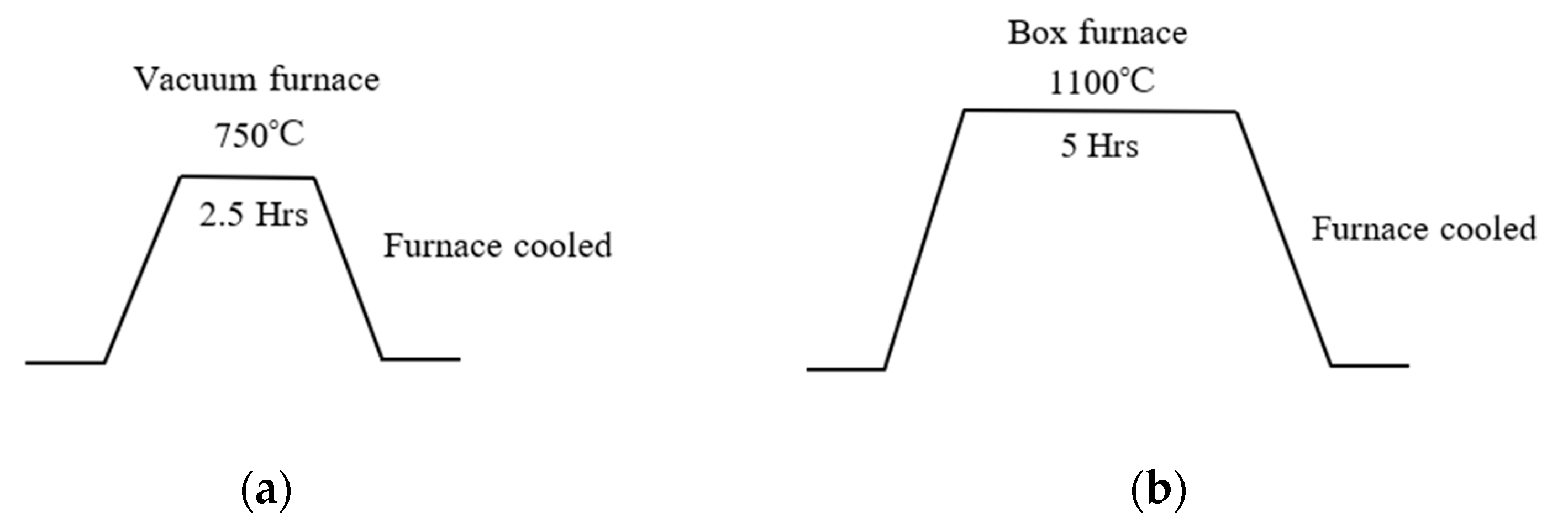
Figure 2.
(a) Schematic drawing of the fabricated micro-sized cantilever beam for Specimens A and B using focus ion beam. (b) Schematic illustration of the test set up for the shearing test using a flat punch diamond indenter on the free end of the microcantilever beam for both specimens, where the blue arrow indicates the direction of the indenter movement.
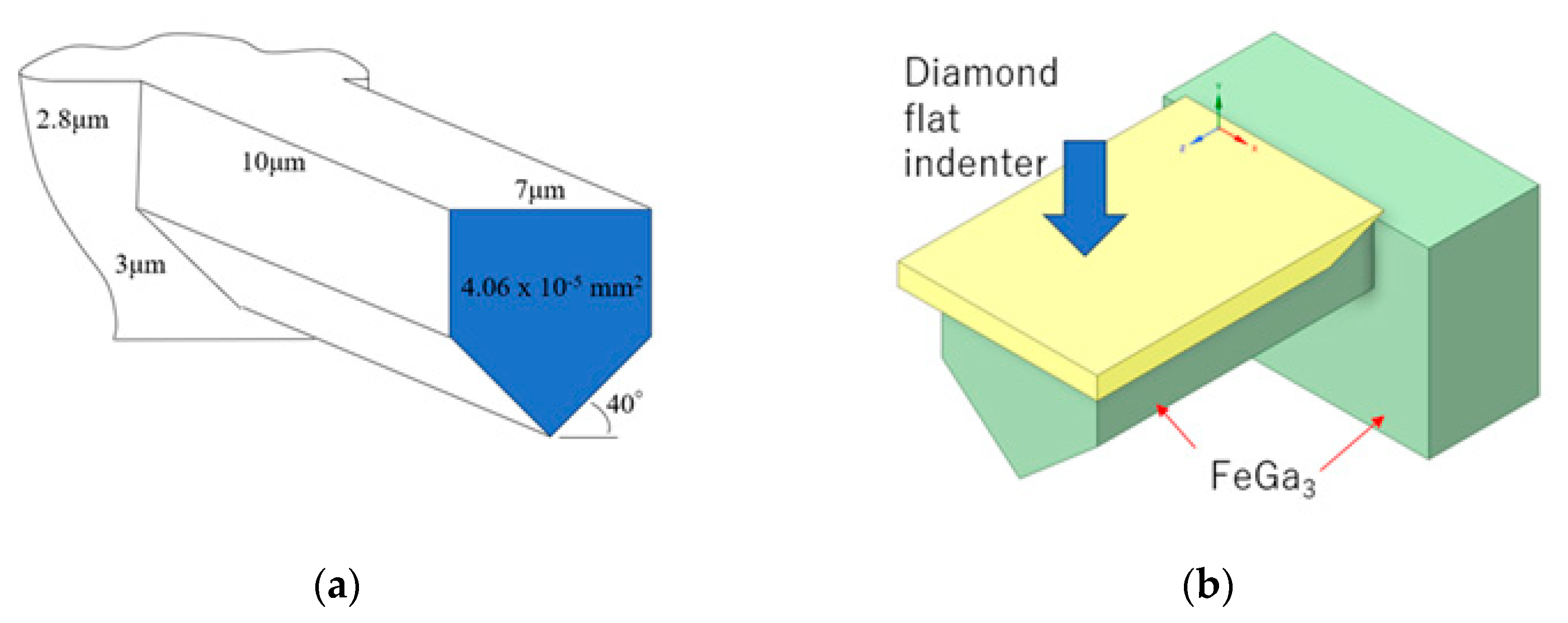
Figure 3.
Enlarged SEM images showing the top surface of (a) Specimen A and (b) Specimen B after heat treatment. Phase identification of (c) Specimen A and (d) Specimen B, showing the XRD pattern. (e) Enlarged XRD pattern of the red boxed area in (c,d).
Figure 3.
Enlarged SEM images showing the top surface of (a) Specimen A and (b) Specimen B after heat treatment. Phase identification of (c) Specimen A and (d) Specimen B, showing the XRD pattern. (e) Enlarged XRD pattern of the red boxed area in (c,d).
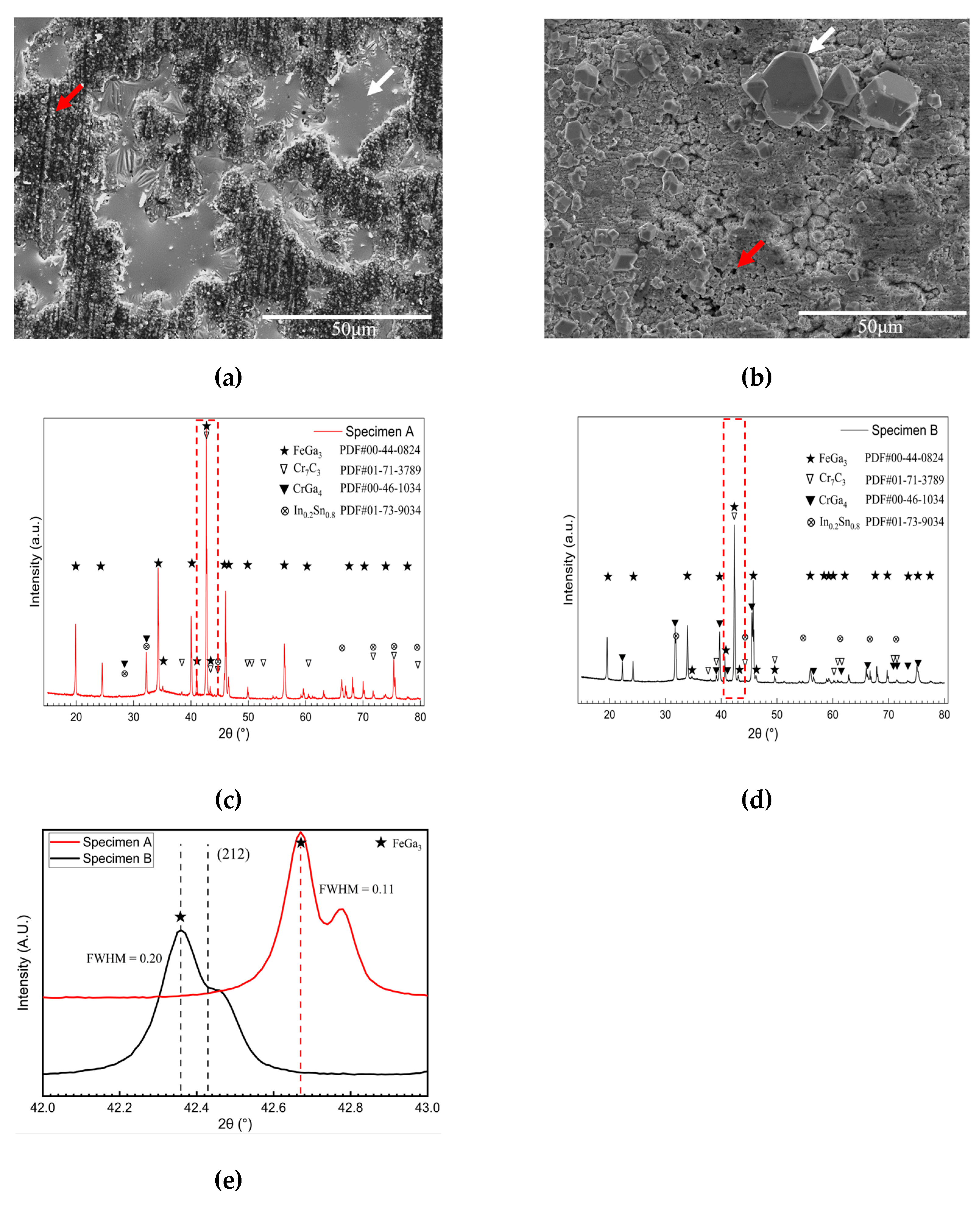
Figure 4.
SEM images showing the cross-sectional surface after the heat treatments; (a) and (b) Cross- sectional morphology of Specimens A and B. (c) and (d) Enlarged BSE images taken from the centre of Specimen A and Specimen B, showing the presence of carbide particle and voids in Specimen A, grain size for both specimens, as well as the indent size at 1 mN load. (e) Enlarged SEM image, showing the interface between the FeGa3 surface film and the SKD11 substrate. (f) Enlarged SEM image of the top surface of Specimen B, showing the polygonal-shaped structure.
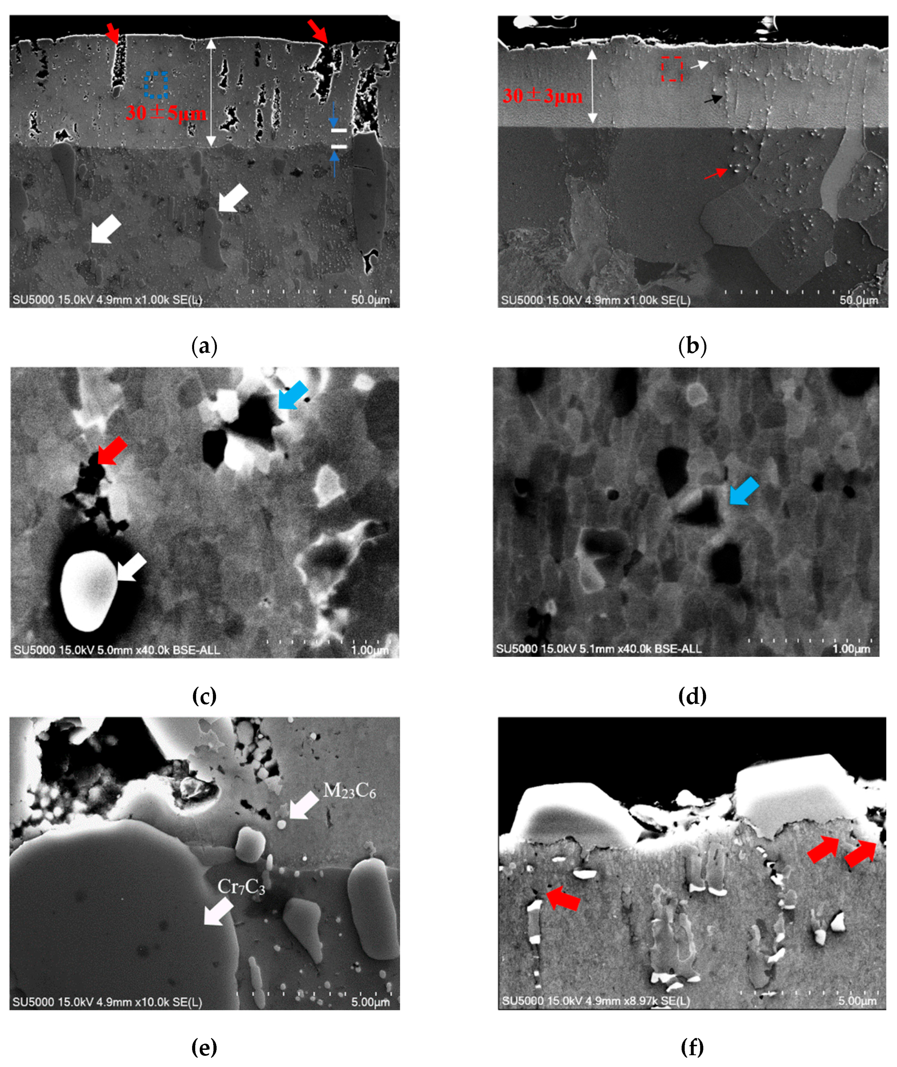
Figure 5.
SEM image and EDS maps of the cross-sectional chemical composition in the reaction layer for Specimen A.
Figure 5.
SEM image and EDS maps of the cross-sectional chemical composition in the reaction layer for Specimen A.
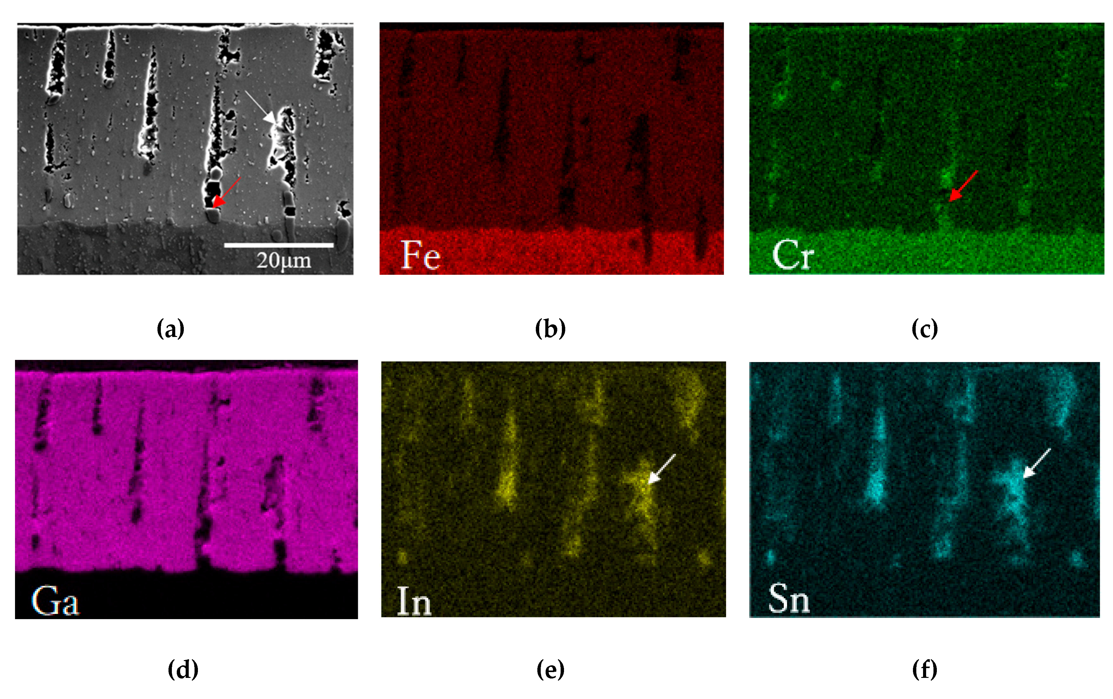
Figure 6.
SEM image and EDS maps of the cross-sectional chemical composition in the reaction layer of Specimen B.
Figure 6.
SEM image and EDS maps of the cross-sectional chemical composition in the reaction layer of Specimen B.
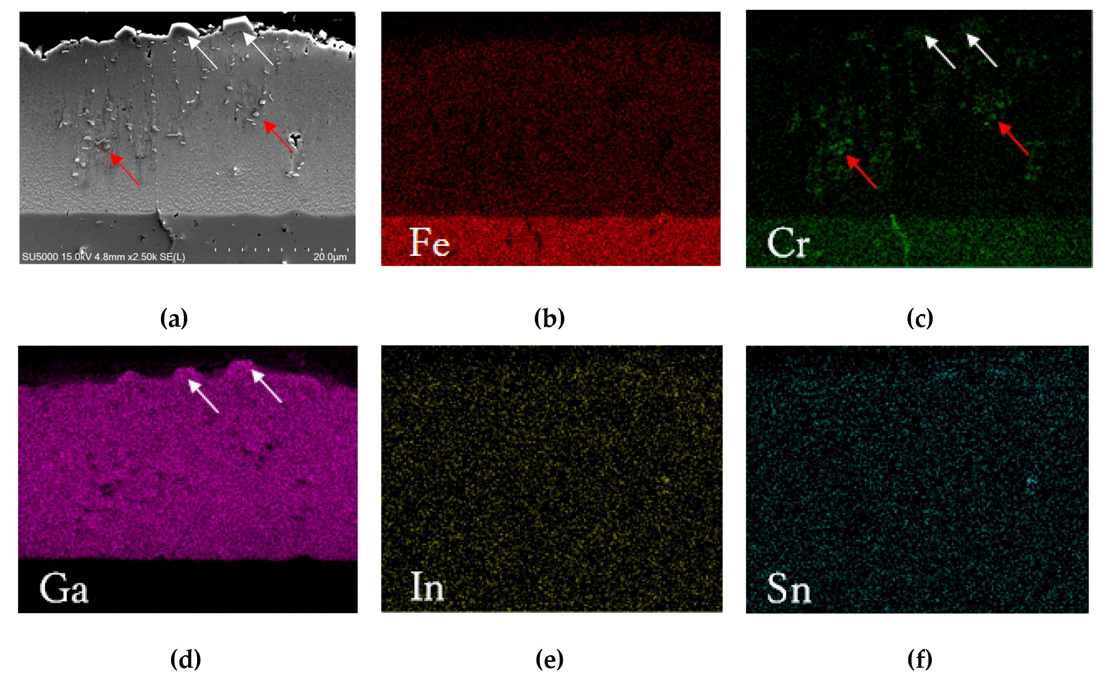
Figure 7.
Some mechanical properties obtained from nanoindentation tests for Specimens A and B. (a)Average nanohardness with different indentation loads. (b) Young’s modulus with different indentation loads. (c) The projected indentation area at different indentation loads, based on the function of indentation depth. (d) Nanohardness across the surface film towards the substrate. (e) Young’s modulus across the surface film towards the substrate. Nanoindentation tests on the cross-section of the compound layer were conducted using a load of 1 mN, while those of the substrate were conducted using a load of 5 mN.
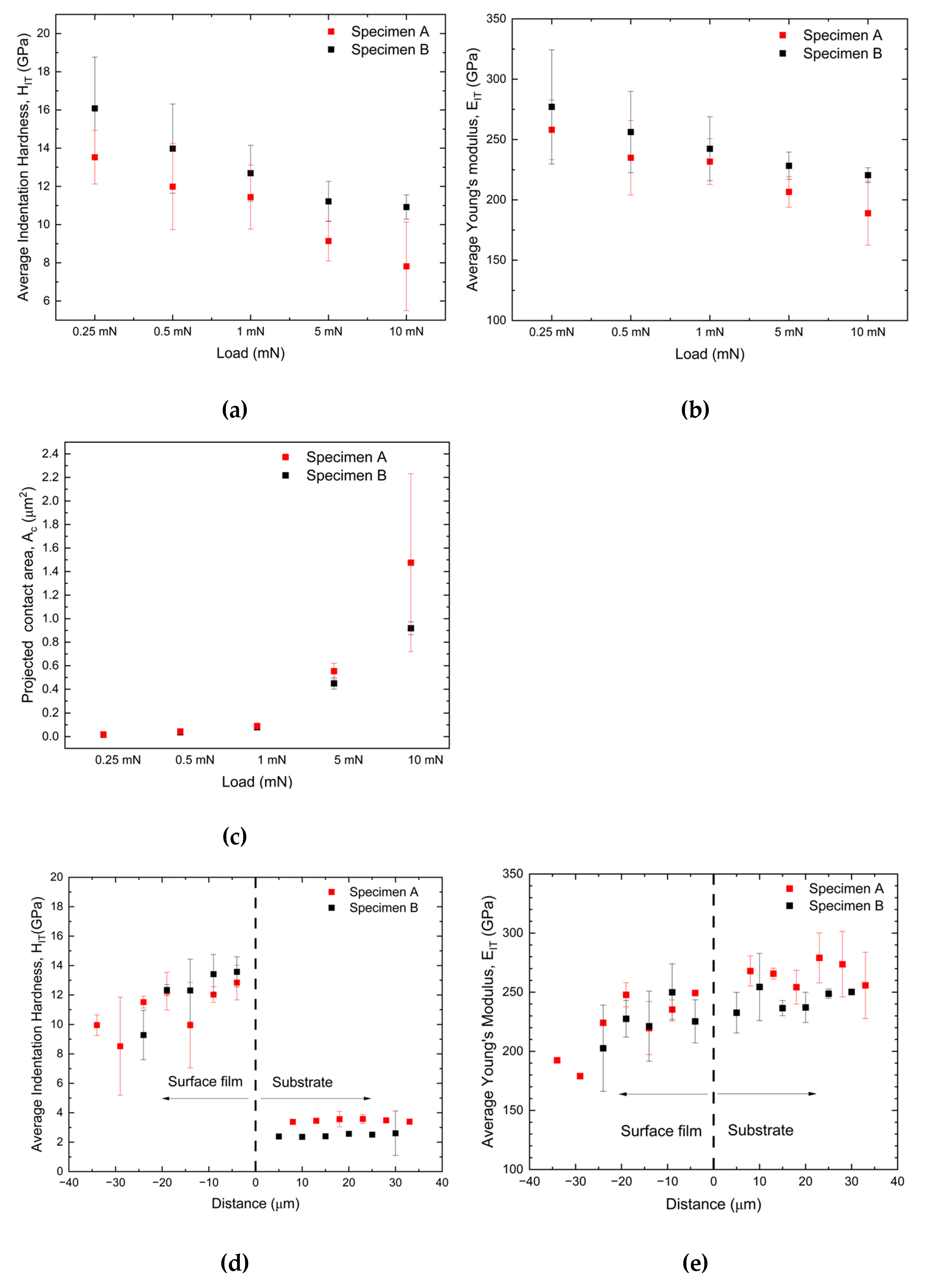
Figure 8.
SEM images of the fabricated cantilever at the interface of (a) Specimen A and (b) Specimen B before the shearing test. SEM images showing the fractured cantilever for (c) Specimen A and (d) Specimen B after the shearing test at the interface.
Figure 8.
SEM images of the fabricated cantilever at the interface of (a) Specimen A and (b) Specimen B before the shearing test. SEM images showing the fractured cantilever for (c) Specimen A and (d) Specimen B after the shearing test at the interface.
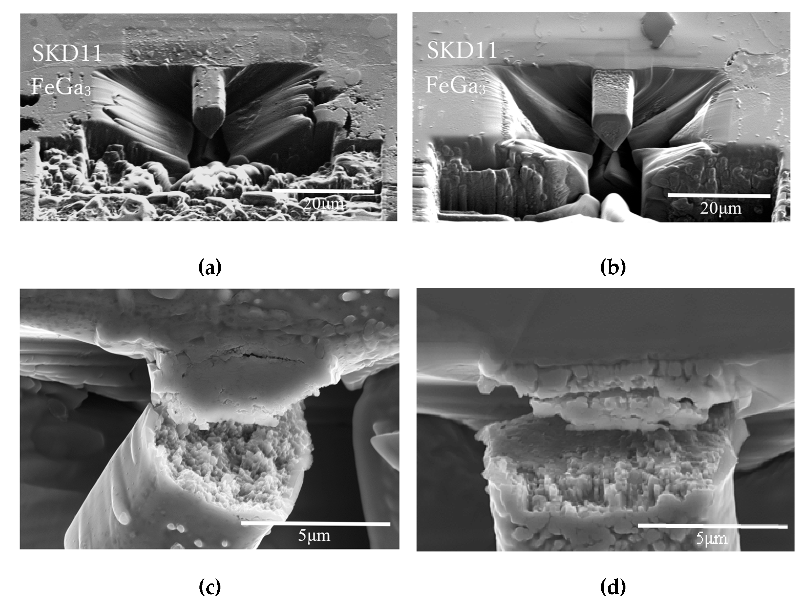
Figure 9.
(a) and (b) show the SEM images of the fabricated cantilever before the shearing test for Specimen A and Specimen B, respectively. (c) Enlarged image of the fractured surface of the cantilever in Specimen A. (d) SEM image of the fractured, porous top surface of Specimen B.
Figure 9.
(a) and (b) show the SEM images of the fabricated cantilever before the shearing test for Specimen A and Specimen B, respectively. (c) Enlarged image of the fractured surface of the cantilever in Specimen A. (d) SEM image of the fractured, porous top surface of Specimen B.
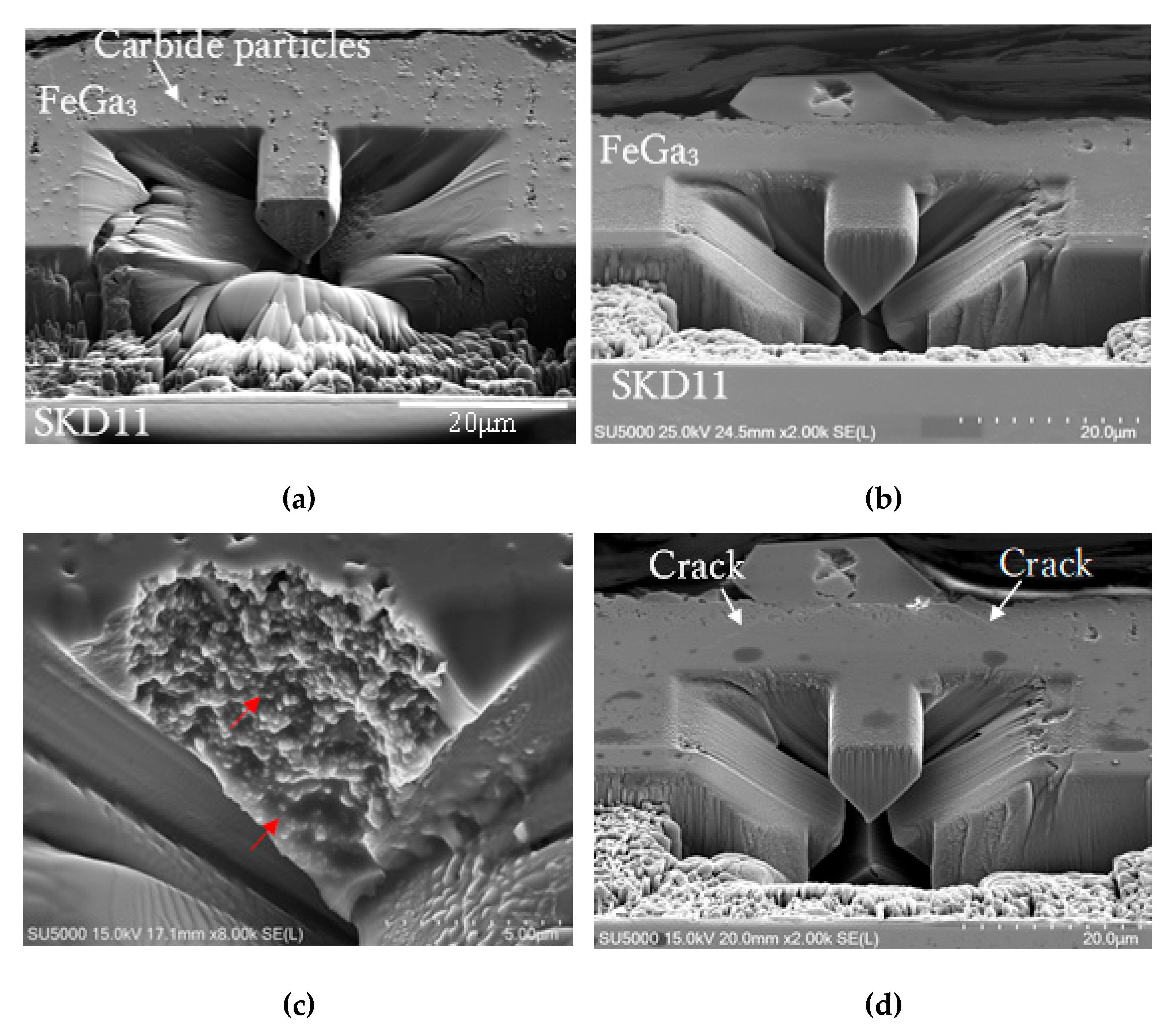
Figure 10.
Load-displacement curves for the shear test on Specimens A and B. The cantilever was formed (a) at the interface between the substrate and the respective FeGa3, (b) at the centre of the FeGa3 compound layer.
Figure 10.
Load-displacement curves for the shear test on Specimens A and B. The cantilever was formed (a) at the interface between the substrate and the respective FeGa3, (b) at the centre of the FeGa3 compound layer.
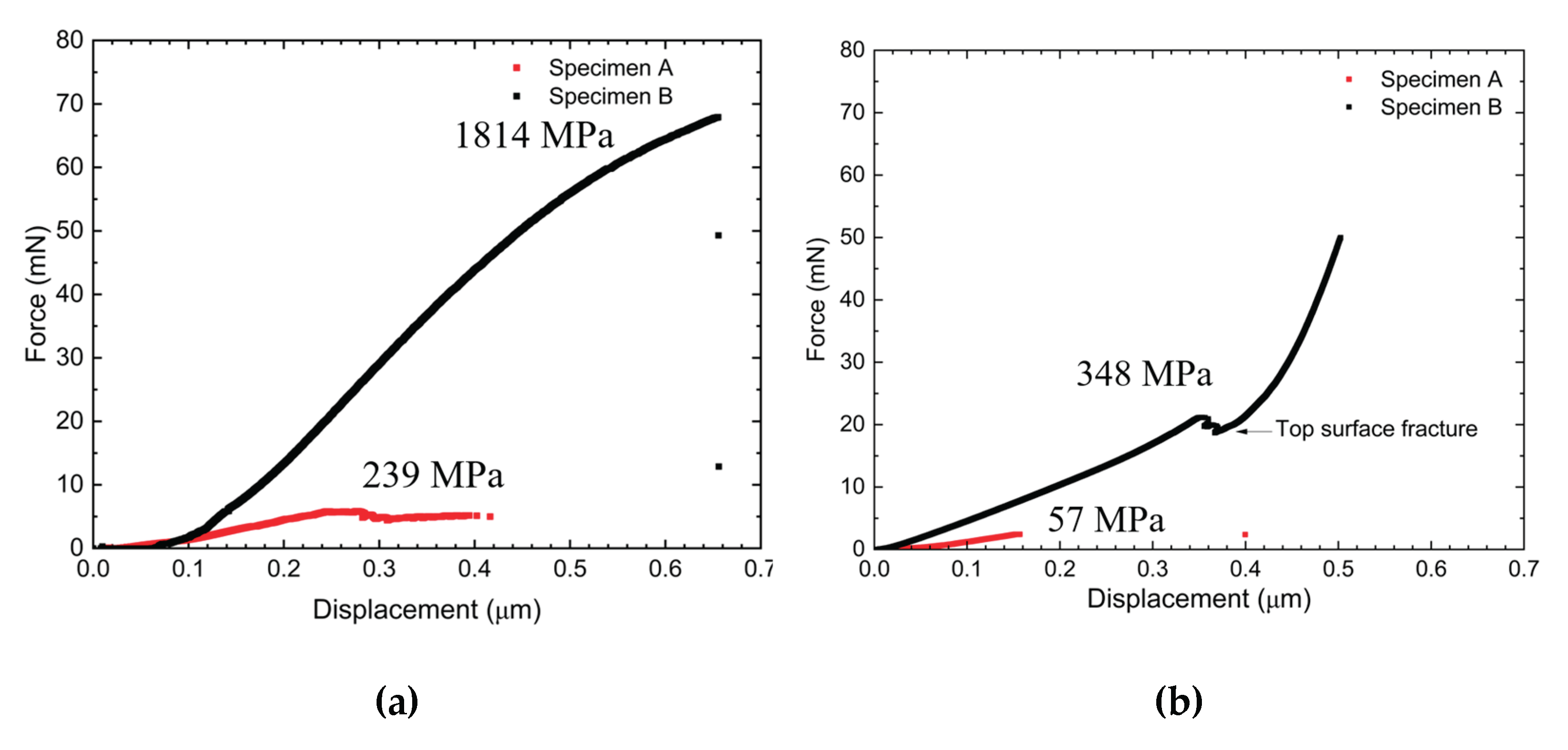

Table 1.
Chemical compositions of the SKD 11 (mass %).
Disclaimer/Publisher’s Note: The statements, opinions and data contained in all publications are solely those of the individual author(s) and contributor(s) and not of MDPI and/or the editor(s). MDPI and/or the editor(s) disclaim responsibility for any injury to people or property resulting from any ideas, methods, instructions or products referred to in the content. |
© 2025 by the authors. Licensee MDPI, Basel, Switzerland. This article is an open access article distributed under the terms and conditions of the Creative Commons Attribution (CC BY) license (http://creativecommons.org/licenses/by/4.0/).
Copyright: This open access article is published under a Creative Commons CC BY 4.0 license, which permit the free download, distribution, and reuse, provided that the author and preprint are cited in any reuse.


