Submitted:
19 August 2025
Posted:
21 August 2025
You are already at the latest version
Abstract
Ultrasonic guided waves interdigital transducers realized with piezoelectric materials are of interests for Structural Health Monitoring systems because their capability of Lamb wave mode selection respect to single element transducers. Besides this advantage the coverage of large areas with minimum number of elements is an important challenge and the problem of efficient excitation with integrated electronics must be solved. This work proposes an electrical matching network topology made of L and C passive components that can be designed for the tradeoff between electrical to mechanical conversion efficiency and bandwidth. The network circuit is analyzed considering the equivalents transducer impedance and the output impedance of the driving electronics. The design rules derived by the transfer function analysis are described and a case study for a piezopolymer IDT is presented. Finally with the implementation of the integrated matching network with the connector of the IDT the effect of cable capacitance is minimized. In conclusion the article is a contribution for using IDT efficiently and in a versatile mode for different electronic front-ends that usually operate at low power supply voltage.
Keywords:
interdigital transducer
; matching network
; ultrasonic guided wave
; equivalent electric impedance
; integrated driving electronic
; network integration
; structural health monitoring
1. Introduction
Ultrasonic guided wave interdigitated transducers (UGWIDT) are increasingly used in SHM systems [1,2,3] for the monitoring of both composite [4,5] and metallic [6] laminar structures, due to their ability to select propagation modes useful for detecting and monitoring mm- and sub-mm-sized defects.
To cover large areas with a limited number of transducers, it is necessary to be able to shape the beam while simultaneously ensuring high transmitted power to ensure a good signal-to-noise ratio [7,8]. To maximise the power the UGWIDT must be well matched with the driving electronics.
UGWIDTs are piezoelectric devices designed to operate at defined frequencies with narrow bandwidth (typically tens of kHz). Typically, SHM systems are designed with operating frequencies selected in the 100 kHz–1 MHz range based on the characteristics of the laminate and therefore the dispersion curves.
Fabricating UGWIDTs with thin (20 μm–200 μm) piezoelectric materials (piezopolymer films [5], spray deposition [9], piezocomposite [10]) in the above frequency range, results in a non-resonant piezoelectric device, meaning its equivalent electrical impedance is well approximated by an ohmic-capacitive impedance . The resistive part of the impedance represents the conversion of electrical excitation power into mechanical power and includes also the piezoelectric material losses; the capacitance depends on the dielectric constant of the piezoelectric material, the thickness, and the area of the electrode design and it is frequency dependent.
The objective of this work is to analyze a modified version of a resonant matching network inserted between the driving circuit and the impedance of UGWIDT. The design goal is to achieve a compromise between the desired bandwidth and power transfer/conversion, also considering the characteristics of the driving electronic circuit while keeping the network as simple as possible. From the following analysis, a design methodology is proposed that allows UGWIDTs to be driven with low-voltage driver circuits (e.g., <24 V), with the advantage of avoiding high-voltage power supply circuits.
Matching networks for UGWIDTs require alternative solutions to those traditionally used for ceramic resonant transducers [11,12]. For the latter, a compensating inductor is used, either in parallel or in series with the transducer. Its electrical impedance is well represented by the resonant circuit model proposed by Kino-Mason in [11]. As is well known, for these transducers, the value of the compensating inductance essentially cancels the effect of the capacitive component at the resonant frequency (series or parallel) and make the load impedance equivalent purely resistive. For narrowband systems, matching networks are used to adapt the transducer impedance to the front-end electronics and typically for single-element transducers passive networks with L, C and magnetic transformers components are used. The magnetic transformer solution is well known but requires the replication of transformers for the number of elements that constitute the UGWIDTs network of the SHM system. In addition to the poor repeatability of the characteristics and the cost, there is an increase in weight and the reliability factor that discourages the adoption of this solution. However, the advantage of the transformer lies in the possibility of increasing the excitation voltage of the piezoelectric transducer starting from a driving with low voltage signals. The matching network design for wide bandwidth piezoelectric transducers is even more complex network [13] and a recent review of the matching network for ultrasonic transducers is reported in [14].
In the case of UGWIDT transducers, the classic solutions mentioned above can be adopted, but since the resistive portion of the impedance is generally higher than that of ceramic transducers, it is difficult to transfer electrical power to a high-value resistive load without increasing the excitation voltage to such values that require a more complex electronic driving circuit. Furthermore, the ideal matching network should be able to match different values of the output impedance of the driving circuit, which can vary greatly depending on the solution adopted: pulsers with power MOSFET devices or linear amplifiers [15,16]. This aspect will also be considered when choosing the matching network topology.
This paper presents a solution that introduces a resonant matching network with the UGWIDT equivalent impedance in parallel to the inductor of the resonant circuit. A matching network design methodology is presented that can be applied to different UGWIDT fabrication technologies based on bandwidth, source impedance, and conversion efficiency requirements.
Finally, the presented design solution, based only on passive L and C components, will also be evaluated for an integrated implementation on the UGWIDT connector to minimize costs, size, and weight. Some examples are therefore reported in the experimental section regarding UGWIDTs made of piezopolymer film (PVDF), since this material is very versatile for the construction of SHM systems but is not as efficient at generating UGWs compared to piezocomposite materials.
2. Matching Network with a Double Tuning Resonant Circuit
For an UGWITD it can be assumed that according to the interdigital finger geometry shown in Figure 1, the equivalent electrical capacitance can be estimated by the well-known formula:
where t is thickness of the piezoelectric material, A active area of the UGWIDT and is the relative dielectric constant of the piezoelectric evaluated at the operating frequency f and temperature T.
According to Figure 1, active area A can be calculated as:
A = L*W*N
By applying the KLM model [11] for an IDT, the equivalent resistance of the electrical impedance can be estimated to be associated to the conversion of the active electrical power provided to the UGWIDT and the power losses of the material at the given operating temperature T and frequency f.
The matching network circuit proposed in this work is based on a composite resonant L-Ca circuit where the transducer impedance is connected in parallel to the inductor L, as shown in Figure 2. The advantages of this topology will be explained in the following, but we can immediately notice that the capacitor Ca provides isolation from the eventual DC component in the driving signal Vin and the inductor L is a short circuit for the DC components of Vout. For completeness of the topic the solution for a matching network of a capacitive – resistive load to a resistive voltage source can also be done with two inductors [17], (Ca is replaced by a second inductor) but it is more expensive, bulky and it is a short circuit for the eventual DC component in the driving signal Vin.
The transfer function of the circuit shown in Figure 2 can be solved by MATLAB symbolic equation tools and can be obtained the following expression in the Laplace domain (s=jω=j2πf):
The analysis of the denominator of (3) shows a main resonant effect for the angular frequency .
The transfer function evaluated for is simplified to two terms and can be analyzed for new insights relative to the design of the matching network.
In (4) we can observe that the first term in brackets depends only on the UGWIDT electrical impedance determined by and , and the second term represents a gain factor that can be adjusted by the choice of . Once is defined, the desired value for can be tuned by the value of L. The possibility to tune and L separately is the advantage of the proposed circuit topology for the matching network.
The increase in the gain factor by causes a decrease of the input impedance at the input port (see Figure 2) as reported in (5):
In (5) we also observe that the variation of and have independent effects on the two additive terms. Moreover, a decrease of has the effect of partitioning the open circuit available voltage of the driving circuit with the finite value of output impedance as shown in Figure 3.
In (5) the denominator shows a series resonant effect on the impedance with a local maximum at the angular frequency . The difference between and depends on the G; this double resonant effect must be considered for the design of the matching network and exploited to obtain the best trade-off.
Ideally a matching network is connected directly to the source (driving electronic circuit) with with different output impedance . In practice the matching network will be connected to the source and the UGWIDT by cables with the line impedance. For the frequency range of interest, we can simplify the effect of the connection line with a capacitor in parallel at the input port Vin of the matching network (see Figure 4). We anticipate this circuit that will be treated in detail in section 2.
For the sake of completeness, we can observe that the series of capacitors Ca and Cb forms a voltage divider for Vout; this circuit network is for matching load at radiofrequency solving the problem of tuning and matching separately [18]. The higher values of Ca (up to several nF) has an impact on the circuit footprint, volume and cost but the value of the desired resonant frequency is obtained with a lower value of L, which is an advantage especially when current in order of 0.1A – 1 A are required for driving with sufficient power the UGWIDT.
2.1. Parametric Simulations of the Matching Network
2.1.1. UGWIDT Electrical Impedance
In this work we consider the design of an UGWIDT with finger electrode pitch S=4mm operating at 450 kHz for defect detection in a Carbon Fiber Reinforced Plastic (CFRP) laminate. The electrode design characteristics are reported in Figure 1. The dimensions of the finger electrodes are S=4mm; W=1,5 mm; L=14mm; N=3. The corresponding central wavelength λ = 2 S = 8 mm. The piezopolymer film was a gold metallized PVDF film with thickness t=100 µm and the finger electrodes geometry shown in Figure 1 realized by laser ablation [19]. The UGWIDT electrical impedance was measured with the UGWIDT mounted on the CFRP cross-ply laminate as shown in Figure 5.
The results for the electrical impedance is a series circuit . This pair of values for and , corresponds to the electrical impedance of one section of the UGWIDT measured either from V+ or V- to ground (GND), as shown in Figure 6
In the next section we will use these values for parametric simulations to explain the results of the formal analysis of the transfer functions.
2.1.2. Parametric Simulations for Ca, Rs
The first parametric simulation regards the matching network shown in Figure 3.
The aim is the evaluation of the influence of the choice of the value of Ca for the fixed values of and.
The value of L=120µH is determined by the desired value , where as reported in section 2.1. We consider also an inductor series resistance ESR=0.16 Ω derived from data sheet of a commercial component. The source resistance Rs=4 Ω is initially chosen choice considering a linear power amplifier [20,21]. By the definition of that depends on , is expected a variation of with the parametric simulation for . The analysis of transfer function around 450 kHz will point out this behavior of the magnitude according to (4).
In Figure 7 is reported the simulated magnitude of the transfer function for from right to left.
From Figure 7 we observe that the maximum value of the transfer function increases with Ca and the evaluation of the magnitude at 450 kHz is reported in the following Table 1.
Choosing the higher value of Ca equal to 1000 pF provides an amplitude gain factor G= 4.76 and a transfer function amplitude of 8.79. This value of Ca is not a limit for the choice, but it is a good compromise for the component footprint and parasitic.
Figure 6 shows also the effect on the bandwidth of the driving signal that must match the UGWIDT requirements. Higher values of Ca provide narrower bandwidth: for Ca =1000pF the -3dB bandwidth is 45kHz while for Ca =600pF is 72 kHz.
Another important factor for the analysis of the matching network is the effect of variation of the source impedance Rs. Different driver circuits can have low value as 0.4 Ω, representing for example the case of a MOSFET integrated pulser, much lower to the initially assumed value of 4 Ω for a linear power amplifier. Then a parametric simulation has been done for three values of Rs = [0.4,1, 4] Ω with a fixed value of Ca =1000pF. The voltage source Vs (see Figure 3) has 15V amplitude, being compatible with integrated driving circuits. The evaluation of the voltage amplitude Vout at the load is reported in Table 2.
The results in Table 2 validate the approach of having a matching network that increases the input voltage from 15 V of a factor 8.7 and is largely independent from the source resistance RS.
2.1.3. Capacitive Effect of Connection Cable and refinement of Ca
In the theoretical analysis we neglected the effect of the connection cable between the driving electronic circuit and the UGWIDT. In general, this connection for a differential driving of and UGWIDT (see V+ and V- in Figure 6) is realized with a twisted pair shielded cable. Depending on the length and dielectric of the insulation materials, we evaluated the capacitance in parallel to the transducer of about CbOUT=170 pF for 1.2 m length.
Including the cable capacitance in the simulation (see Figure 8), the value of Ca must be optimized for the operating frequency of 450 kHz. In the solution proposed in Figure 8, the matching network is located on the board of the electronic circuit and the signal Vout and GND are connected to the transducer by the connection cable. As we will see later in this article, the integration of the matching network on the UGWIDT connector is more convenient because the effect of cable capacitance is reduced.
For the optimization we select by parametric simulation an optimal value of Ca =780pF which maintains a high output voltage Vout on the transducer of 105 V. Accounting for this effect the transfer function magnitude is 105/15=7, lower than 8.79 as evaluated in Table 1 without considering the cable capacitance.
2.2. Experimental Validation of the Matching Network
The designed matching network has been mounted onto the PCB of the driving circuit that is a power linear amplifier [22] and connected with a shielded cable to the UGWIDT described in previous section.
The driving differential signals (V+ and V-) applied to each section of the UGWIDT (see Figure 6) are shown in Figure 9 (top).
The experimental results in Figure 9 (top) show driving signals with amplitude 15.5V amplitude and in Figure 9 (bottom) the corresponding signals after the insertion of the matching network with amplitude of about 100V. The transfer function magnitude experimentally evaluated is 100/15.5=6.45. The estimate is in good agreement with simulations considering that some parasitic of passive components are not considered in the simulations.
2.3. Evaluation of the Input Impedance
The last part of the analysis concerns the estimation of the input impedance at the input port of the matching network.
In Figure 10 the magnitude of the impedance has been simulated, and the minimum is obtained at 450 kHz and its value about 59Ω.
The minimum of Zin=60Ω confirm the little influence of the source impedance that is in general much lower than this value. Then this design approach is versatile for different driving electronic circuits.
3. Integration of the Matching Network on the UGWIDT Connector
In section 2.1.2 the effect of the cable used for the connection between the matching network and the UGWIDT is pointed out. An alternative approach is the realization of the matching network on a PCB that is also used to connect metal fingers to the driving signals. The type of contact between top and bottom PCBs with copper pads and the gold metallized PVDF is guaranteed by the pressure generated by microrivets joining the two PCBs and the PVDF film in the middle [3]. On one of the two PCBs the circuit of the matching network is mounted with low profile, low weight SMD components.
In Figure 11 is illustrated the PCB design and the mounted matching network.
With this change in the connection, now the cable capacitance must be moved in parallel to the input of the matching network as shown in Figure 12.
In the bottom of Figure 12 we can see that at 450 kHz the gain factor evaluated on the magnitude of is 3.8. By simulation we can also observe a change of the Zin that is increased to 91Ω at 450 kHz while the minimum equal to 51 Ω is shifted to 494 kHz. The higher value of the input impedance means the requirement of higher input driving voltage to increase the current in RL. This problem will be tackled in the next section.
4. Pulser Circuit with Matching Network
In the previous section we concluded that the matching network can be designed with adequate gain factor and bandwidth, but the high input impedance limits the power delivered to RL. For this inconvenience, a driving circuit based on an H-bridge with four power MOSFET is an effective solution. This type of electronic circuit is now common also in integrated devices and they can be supplied with a single power supply voltage [23,24,25,26]. The output voltage is doubled across the load thanks to the differential connection.
In a previous project we developed a modular system for exciting array of 16 IDTs [27]. Here we use the same board to test the effectiveness of the matching network for UGWIDT. In Figure 13 the schematic circuit for the simulation is shown.
The excitation signal is a burst of 4 pulses at 450 kHz at 5V. These pulses are then processed to get out of phase correspondent signal by a CMOS inverter (see bottom right of Figure 13). The driving signals (Vleg+ and Vleg-) are obtained with a power supply voltage Vdd=20V. The output signals at the UGWIDT are Vout+ and Vout-.
In Figure 14 the results of the simulations are illustrated.
By simulation we can observe that a burst with an amplitude of 20 V generates a driving signal at one section of the UGWIDT of about 54V. The evaluation of the magnitude is 54/20=2.7. The peak to peak is about 108V. The pulser circuit with differential driving recovers from the limitation of the integrated linear power amplifiers that can drive up to 24V the load at the maximum current.
The simulated results need also to be validated with an electronic circuit board implementing the H-bridge circuit shown in Figure 13 and the matching network realized on a PCB for connecting the piezopolymer UGWIDT.
In Figure 15 are presented the excitation signal with 4 pulses at 450 kHz with 20V amplitude and the corresponding signal on one section of the UGWIDT.
The comparison of the simulations and the experimental results shows that the gain factor and the shape of the output signal are in good agreement, and this solution can be adopted efficiently for driving the input impedance of the matching network.
5. Conclusions
The design of matching networks of UGWIDT fabricated with piezopolymer film is presented. Because of their relatively high impedance at the operating frequencies for SHM system and the low amplitude of the driving signals generated by integrated electronics, a matching network based on a resonant behavior is proposed and analyzed for the specific user case. The theoretical analysis of the transfer function and the input impedance provides insight on how to select the two main components L and Ca of this matching network with the load inserted in parallel to the inductor. In this way we can design separately the value of L for the desired operating frequency and the value of Ca for the voltage amplitude gain factor. The matching network is simple and provides a relatively high impedance with respect to the source, minimizing the effect of performance change depending on the driving electronics. Finally, the solution with an integrated matching network on the UGWIDT connector is presented and the full experimentation with a H bridge pulser demonstrates the effectiveness of this simple solution. The driving voltage up to 100 Vpp can be achieved increasing the signals generated from integrated power amplifiers or pulser, typically in the order of 24V. The design rules and the main trade off are reported so that the design of this type of matching network can be extended for UGWIDTs fabricated with other piezoelectric materials.
Funding
This research received no external funding.
Conflicts of Interest
The author declare no conflicts of interest.
Abbreviations
The following abbreviations are used in this manuscript:
| UGWIDT | Ultrasonic Guided Wave Interdigital Transducer |
| SHM | Structural Health Monitoring |
| IDT | Interdigital Transducer |
| PCB | Printed circuit board |
| PVDF | Polyvinylidene difluoride |
References
- T. Stepinski, M. Mańka, and A. Martowicz, “Interdigital lamb wave transducers for applications in structural health monitoring,” NDT & E International, vol. 86, pp. 199–210, Mar. 2017. [CrossRef]
- B. Ren and C. J. Lissenden, “PVDF Multielement Lamb Wave Sensor for Structural Health Monitoring,” in IEEE Transactions on Ultrasonics, Ferroelectrics, and Frequency Control, vol. 63, no. 1, pp. 178-185, Jan. 2016. [CrossRef]
- P. Giannelli, A. Bulletti and L. Capineri, “Multifunctional Piezopolymer Film Transducer for Structural Health Monitoring Applications,” in IEEE Sensors Journal, vol. 17, no. 14, pp. 4583-4586, 15 July15, 2017. [CrossRef]
- M. Mańka, A. Martowicz, M. Rosiek, T. Stepinski, and T. Uhl, “Tunable interdigital transducers made of piezoelectric macro-fiber composite,” Smart Materials and Structures, vol. 25, no. 11, p. 115022, Oct. 2016. [CrossRef]
- A. Bulletti, P. Giannelli, M. Calzolai and L. Capineri, “An Integrated Acousto/Ultrasonic Structural Health Monitoring System for Composite Pressure Vessels,” in IEEE Transactions on Ultrasonics, Ferroelectrics, and Frequency Control, vol. 63, no. 6, pp. 864-873, June 2016. [CrossRef]
- B. Ren, H. Cho, and C. Lissenden, “A Guided Wave Sensor Enabling Simultaneous Wavenumber-Frequency Analysis for Both Lamb and Shear-Horizontal Waves,” Sensors, vol. 17, no. 3, p. 488, Mar. 2017. [CrossRef]
- V. Giurgiutiu, Structural Health Monitoring with Piezoelectric Wafer Active Sensors. Academic Press, 2014.
- X. Qing, W. Li, Y. Wang, and H. Sun, “Piezoelectric Transducer-Based Structural Health Monitoring for Aircraft Applications,” Sensors, vol. 19, no. 3, p. 545, Jan. 2019. [CrossRef]
- Shifeng Guo et al. 2019 Smart Mater. Struct. 28 075031. [CrossRef]
- Tadeusz Stepinski, Michał Mańka, Adam Martowicz, Interdigital lamb wave transducers for applications in structural health monitoring, NDT & E International, Volume 86, 2017, Pages 199-210,, ISSN 0963-8695, . [CrossRef]
- Kino, Gordon S. (1987). Acoustic Waves: Devices, Imaging, and Analog Signal Processing. Prentice-Hall. ISBN 0130030473.
- A. R. Selfridge, R. Baer, B. T. Khuri-Yakub and G. S. Kino, “Computer-Optimized Design of Quarter-Wave Acoustic Matching and Electrical Matching Networks for Acoustic Transducers,” 1981 Ultrasonics Symposium, Chicago, IL, USA, 1981, pp. 644-648. [CrossRef]
- L. Capineri, L. Masotti, M. Rinieri and S. Rocchi, “Ultrasonic transducers as a black-box: equivalent circuit synthesis and matching network design,” in IEEE Transactions on Ultrasonics, Ferroelectrics, and Frequency Control, vol. 40, no. 6, pp. 694-703, Nov. 1993. [CrossRef]
- V. T. Rathod, “A Review of Electric Impedance Matching Techniques for Piezoelectric Sensors, Actuators and Transducers,” Electronics, vol. 8, no. 2, p. 169, Feb. 2019. [CrossRef]
- H. Zhou, S. H. Huang, and W. Li, “Electrical Impedance Matching Between Piezoelectric Transducer and Power Amplifier,” IEEE Sensors Journal, vol. 20, no. 23, pp. 14273–14281, Dec. 2020. [CrossRef]
- https://www.analog.com/media/en/technical-documentation/data-sheets/lt1210.pdf 15 August 2025.
- M. M. Weiner, Monopole Antennas, Marcel Dekker, Inc.,CRC Press, Rev. Exp edition, New York, pp.110-118, 2003.
- Valery Godyak, RF discharge diagnostics: Some problems and their resolution J. Appl. Phys. 129, 041101 (2021);. [CrossRef]
- L. Bergamaschi, A. Bulletti, M. Dimitri and L. Capineri, “Modelling the beam pattern of piezopolymer interdigital transducers (IDT) for optimizing the off-axis response,” 2022 IEEE International Ultrasonics Symposium (IUS), Venice, Italy, 2022, pp. 1-2. [CrossRef]
- L. Svilainis and G. Motiej?nas, “Power amplifier for ultrasonic transducer excitation,” vol. 58, no. 1, pp. 30-36, Mar. 2006. [CrossRef]
- L. Capineri, “A 15 MHz bandwidth, 60 Vpp, low distortion power amplifier for driving high power piezoelectric transducers,” Review of Scientific Instruments, vol. 85, no. 10, p. 104701, Oct. 2014. [CrossRef]
- J. Zhou and Y. Zheng, “Broadband Linear High-Power Amplifier Based on the Parallel Amplification Architecture for Electromagnetic Ultrasonic Guided Wave,” Sensors, vol. 19, no. 13, p. 2924, Jul. 2019. [CrossRef]
- Y. Guo, C. Aquino, D. Zhang, and B. Murmann, “A Four-Channel, 36 V, 780 kHz Piezo Driver Chip for Structural Health Monitoring,” IEEE Journal of Solid-State Circuits, vol. 49, no. 7, pp. 1506-1513, Apr. 2014. [CrossRef]
- P. R. Smith, D. M. J. Cowell, and S. Freear, “Width-modulated squarewave pulses for ultrasound applications,” IEEE Trans. Ultrason., Ferroelectr.,Freq. Control, vol. 60, no. 11, pp. 2244–2256, 2013. [CrossRef]
- M. Terenzi, D. Ghisu, F. Quaglia, E. Boni, M. Diaz Mendez, M. Valle, and D. D. Caviglia, “Flexible hardware architecture for the generation of ultrasound pulses in medical imaging,” in 2016 IEEE International Ultrasonics Symposium (IUS), 2016, pp. 1–4. [CrossRef]
- P. Giannelli, A. Bulletti, M. Granato, G. Frattini, G. Calabrese and L. Capineri, “A Five-Level, 1-MHz, Class-D Ultrasonic Driver for Guided-Wave Transducer Arrays,” in IEEE Transactions on Ultrasonics, Ferroelectrics, and Frequency Control, vol. 66, no. 10, pp. 1616-1624, Oct. 2019. [CrossRef]
- A. Bulletti, P. Giannelli, M. Calzolai and L. Capineri, “Multielement Interdigital Transducers for Structural Health Monitoring,” 2018 IEEE International Ultrasonics Symposium (IUS), Kobe, Japan, 2018, pp. 1-3. [CrossRef]
Figure 1.
Dimensional parameters of the finger electrodes for a UGWIDT. In the example the number of finger pairs N is 3.
Figure 1.
Dimensional parameters of the finger electrodes for a UGWIDT. In the example the number of finger pairs N is 3.
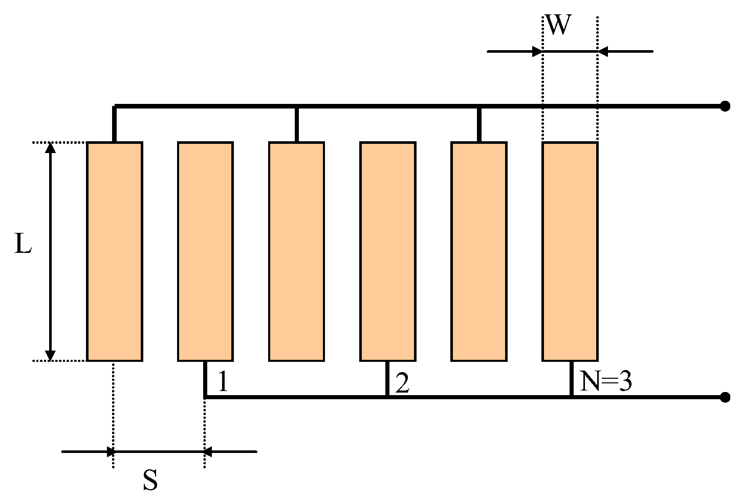
Figure 2.
The equivalent transducer impedance ZL connected in parallel to the inductor L.
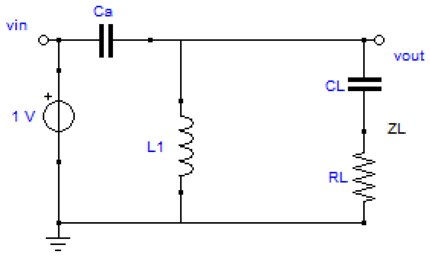
Figure 3.
Matching network connected with the input port Loading effect of input port Vin to the source Vs, Rs and the electrical impedance of the UGWIDT at the output port Vout.
Figure 3.
Matching network connected with the input port Loading effect of input port Vin to the source Vs, Rs and the electrical impedance of the UGWIDT at the output port Vout.
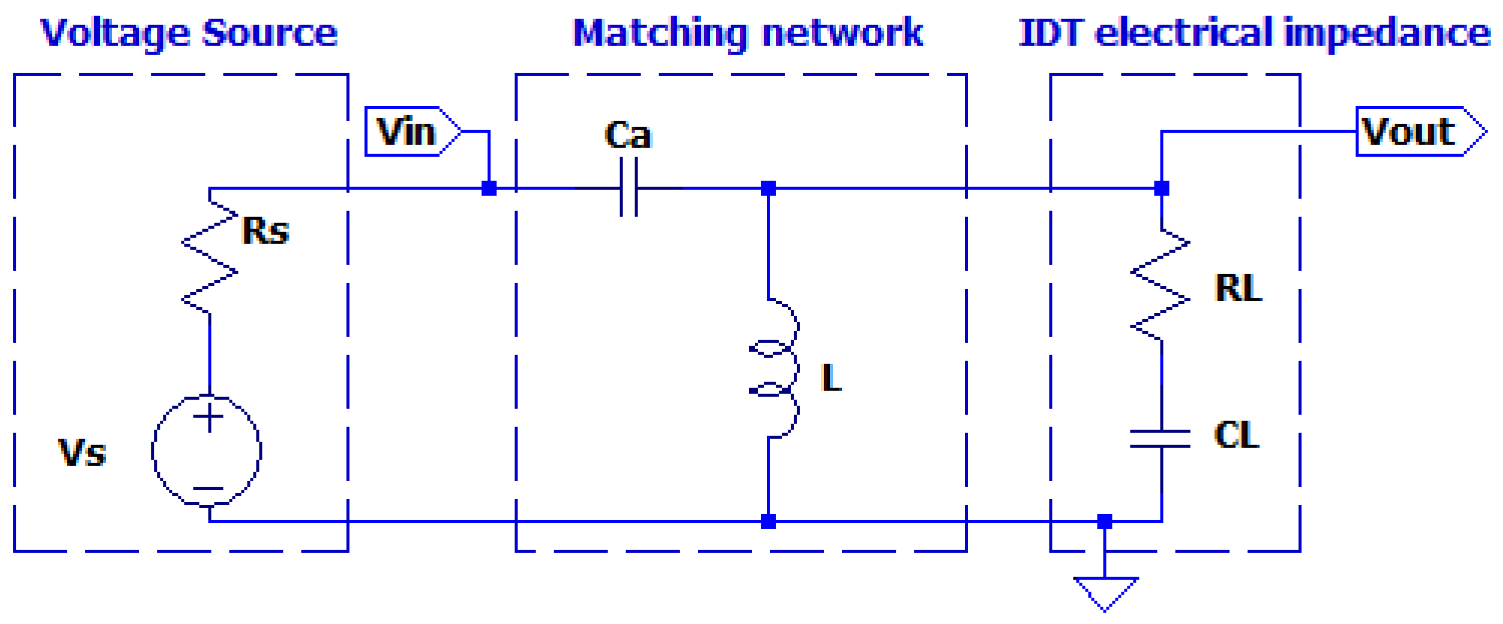
Figure 4.
Schematic circuit for considering the capacitive effect of Cb due to connection cable of the matching network at the input or at the output.
Figure 4.
Schematic circuit for considering the capacitive effect of Cb due to connection cable of the matching network at the input or at the output.
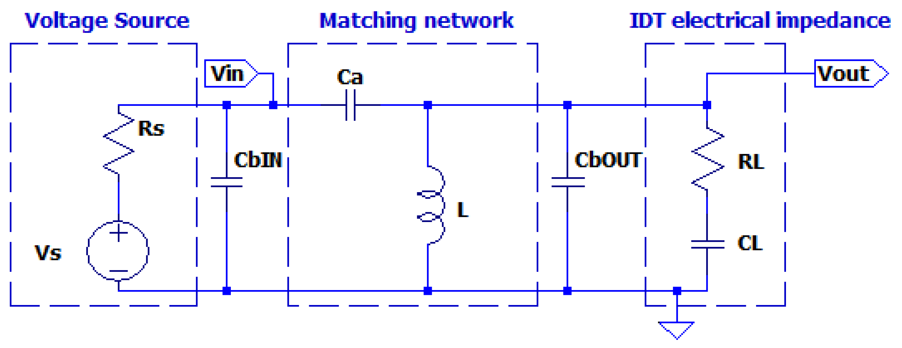
Figure 5.
Measurement of the equivalent electrical impedance at 450 kHz with volt-amperometric method (Voltage probe TEKTRONIX Mod. P3010, current probe P6022 TEKTRONIX). The piezopolymer UGWIDT is bonded to the CFRP cross ply laminate.
Figure 5.
Measurement of the equivalent electrical impedance at 450 kHz with volt-amperometric method (Voltage probe TEKTRONIX Mod. P3010, current probe P6022 TEKTRONIX). The piezopolymer UGWIDT is bonded to the CFRP cross ply laminate.

Figure 6.
Differential driving V+ and V- of the UWGIDT.
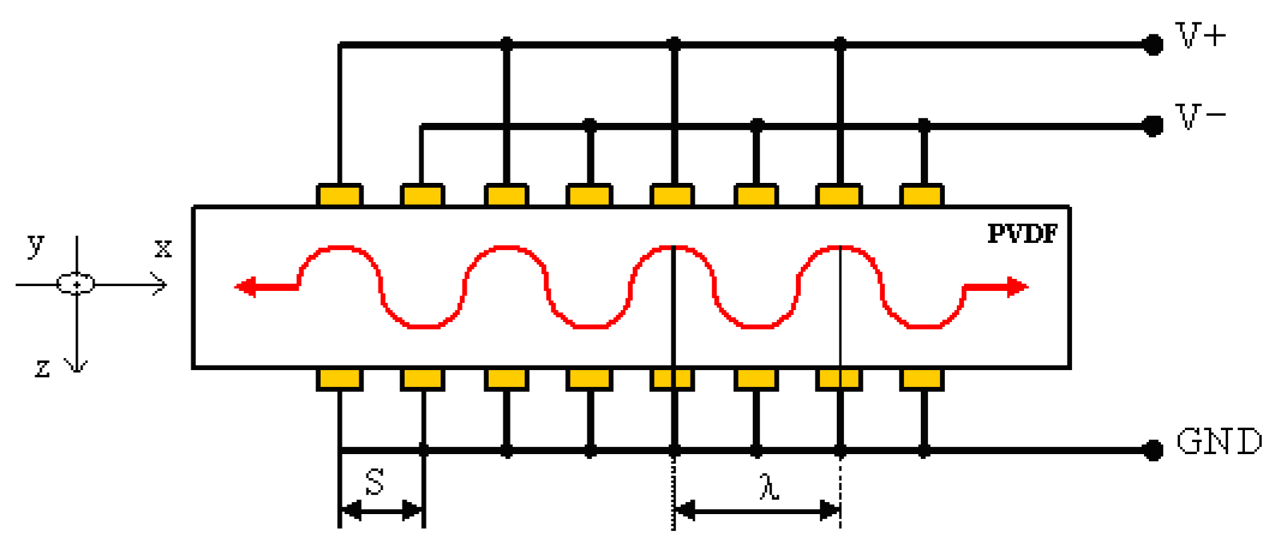
Figure 7.
Simulated transfer function with parametric simulations for Ca.
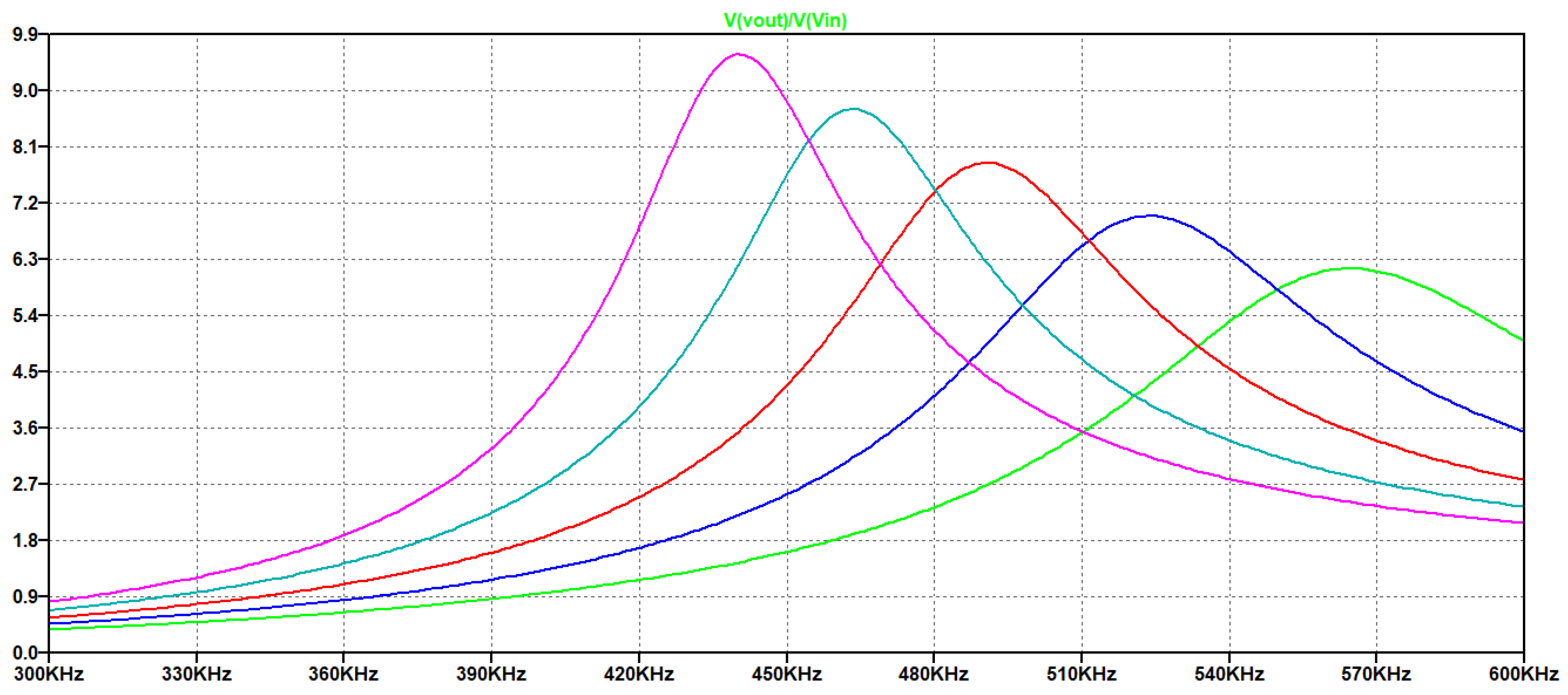
Figure 8.
Simulated matching network including connection cable capacitance CbOUT=170pF.
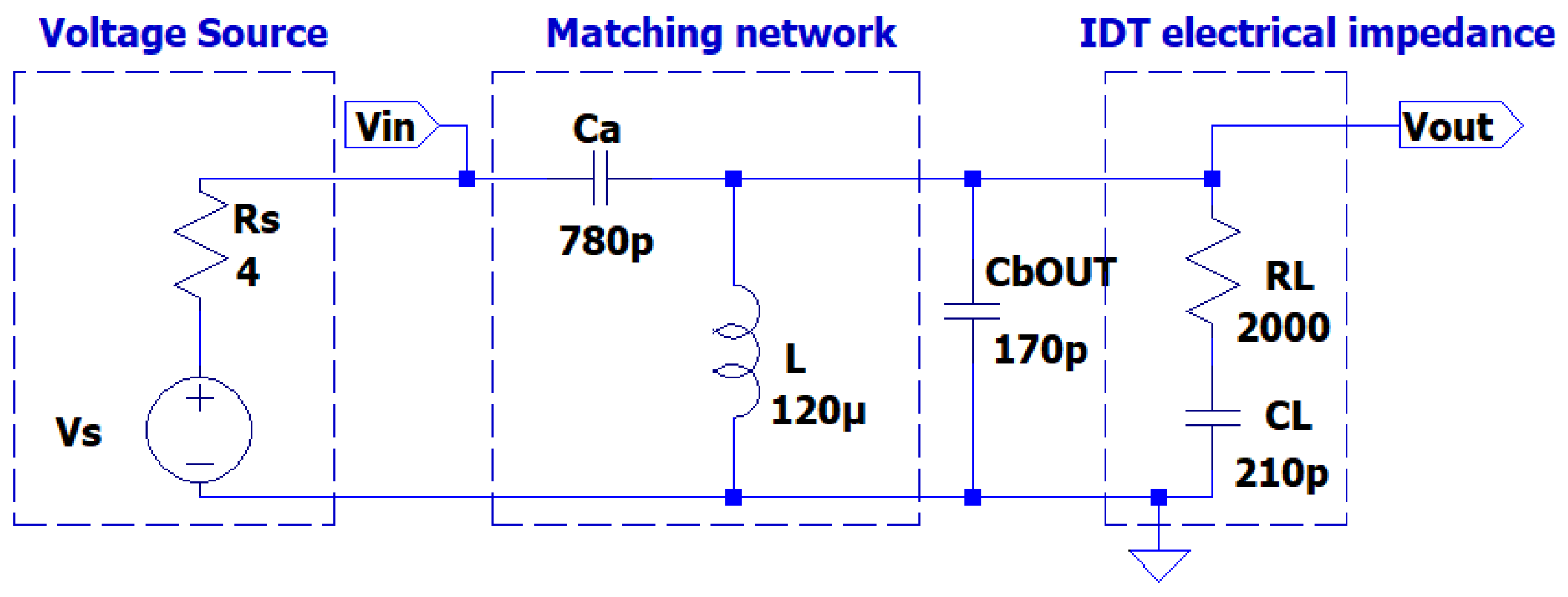
Figure 9.
(Top) driving signals from a linear power amplifier. (Bottom) driving signals with the matching network shown in Figure 8.
Figure 9.
(Top) driving signals from a linear power amplifier. (Bottom) driving signals with the matching network shown in Figure 8.
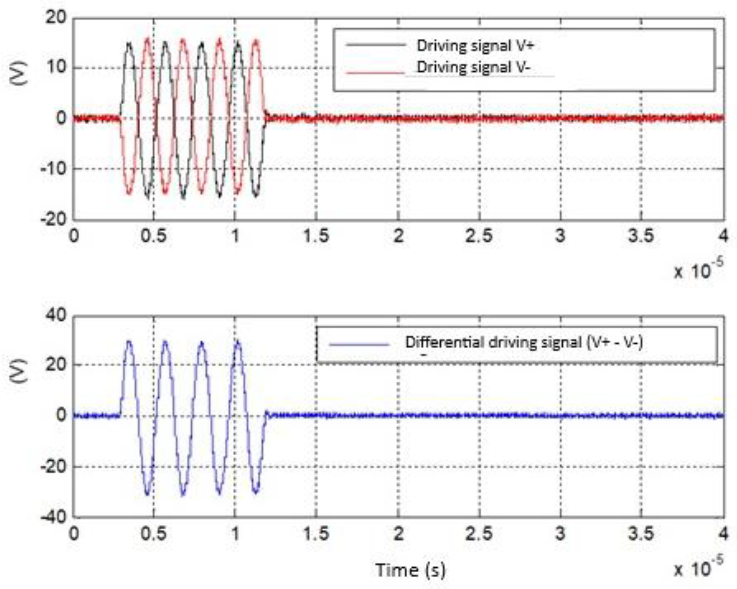
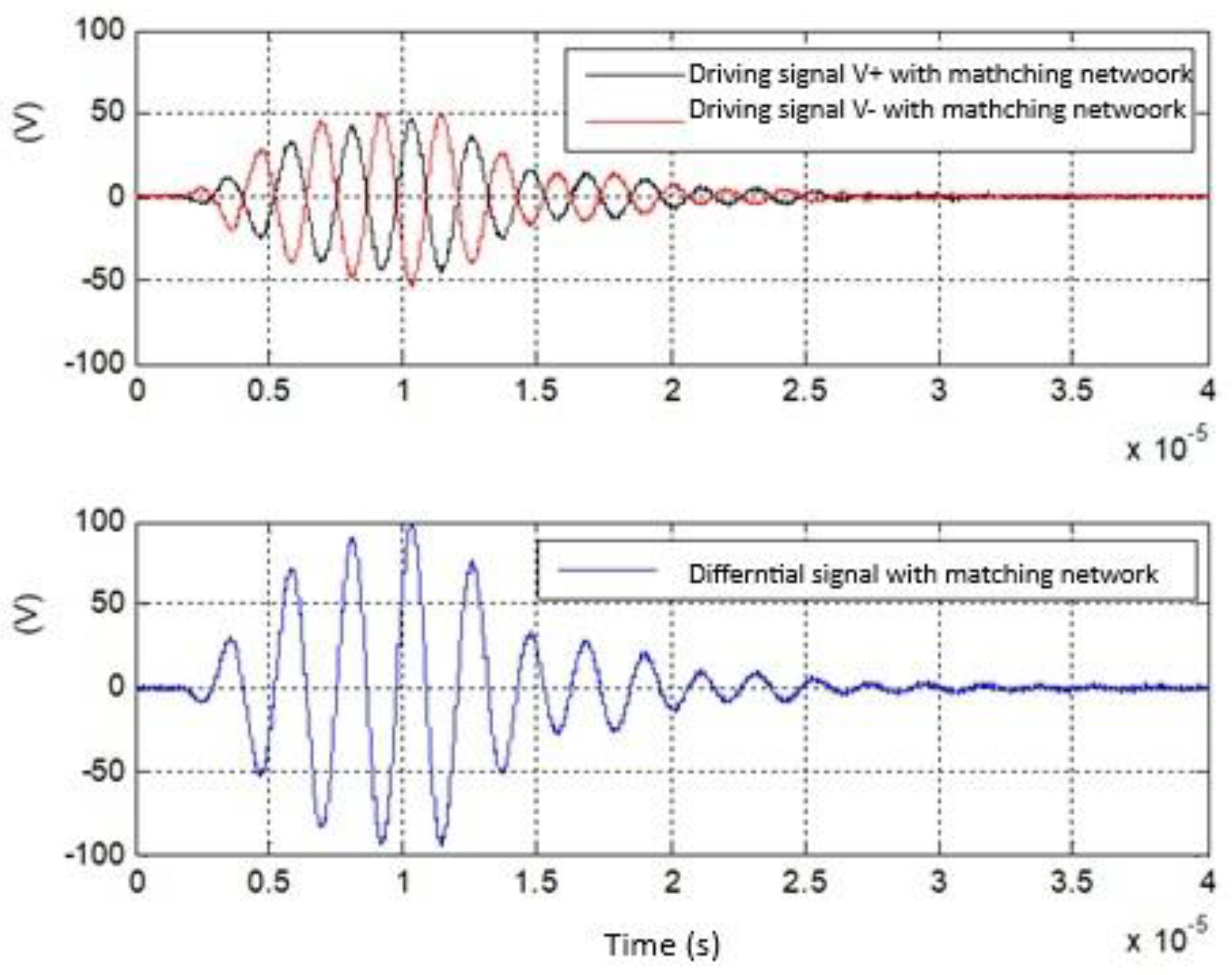
Figure 10.
Magnitude of the input impedance Zin with the matching network.
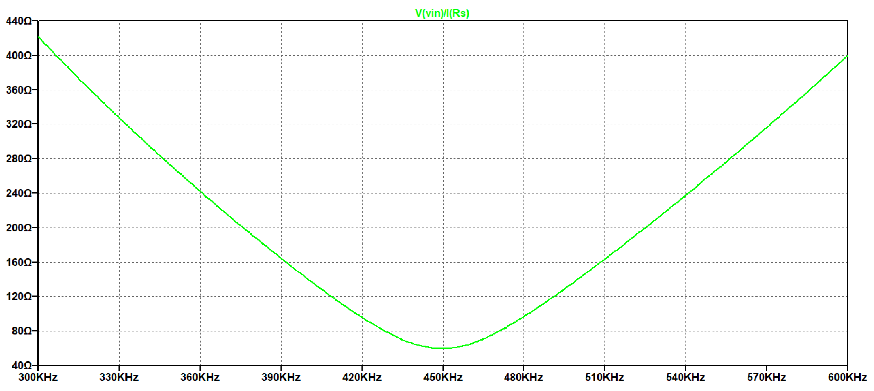
Figure 11.
(a) Final assembly of the matching network with differential output and ground. (b) PCB design for the connector with integrated matching network; dimensions are in mm.
Figure 11.
(a) Final assembly of the matching network with differential output and ground. (b) PCB design for the connector with integrated matching network; dimensions are in mm.

Figure 12.
(Top) schematic of the matching network including connection cable capacitance CbIN=170pF to the driving electronics. (Bottom) Simulated transfer function magnitude.
Figure 12.
(Top) schematic of the matching network including connection cable capacitance CbIN=170pF to the driving electronics. (Bottom) Simulated transfer function magnitude.
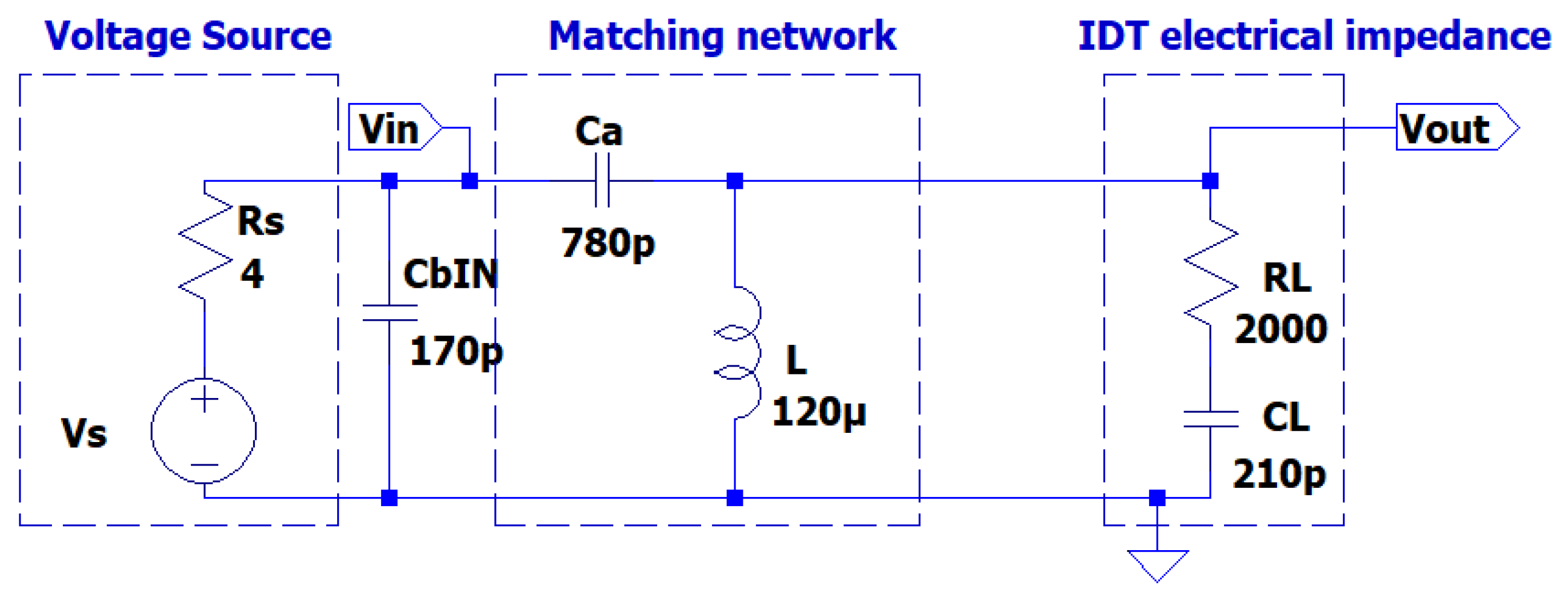
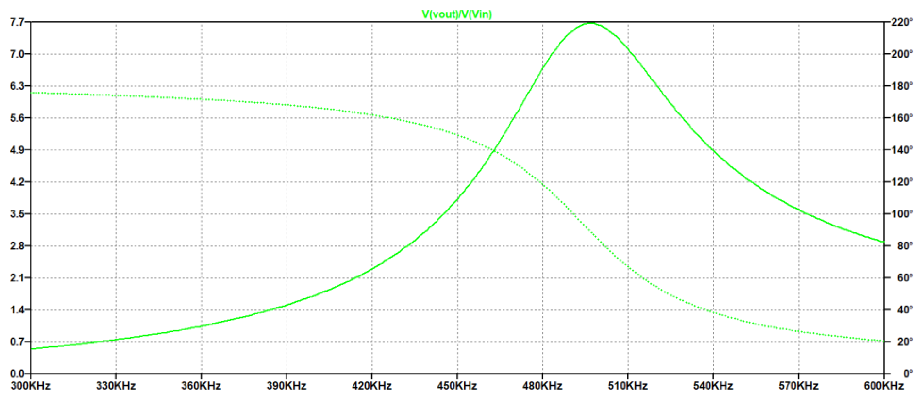
Figure 13.
Simulation of an H-bridge pulser circuit connected to the matching network with a cable capacitance of 170pF.
Figure 13.
Simulation of an H-bridge pulser circuit connected to the matching network with a cable capacitance of 170pF.
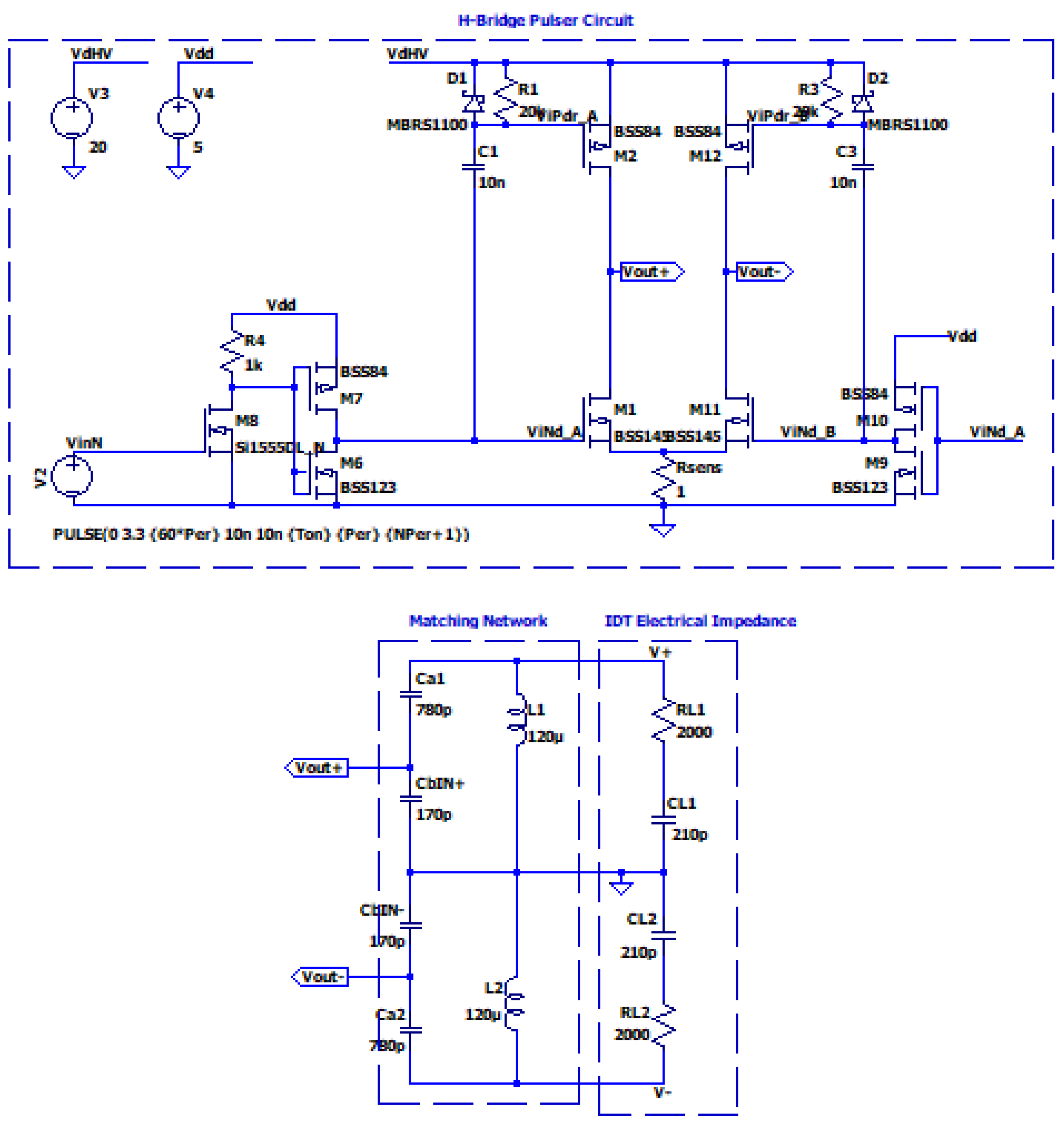
Figure 14.
Simulation results of the excitation with an H. bridge supplied at 20V. (top) Driving signal for one section of the H-Bridge (bottom) Applied output voltage V+ to one section of the UGWIDT.
Figure 14.
Simulation results of the excitation with an H. bridge supplied at 20V. (top) Driving signal for one section of the H-Bridge (bottom) Applied output voltage V+ to one section of the UGWIDT.
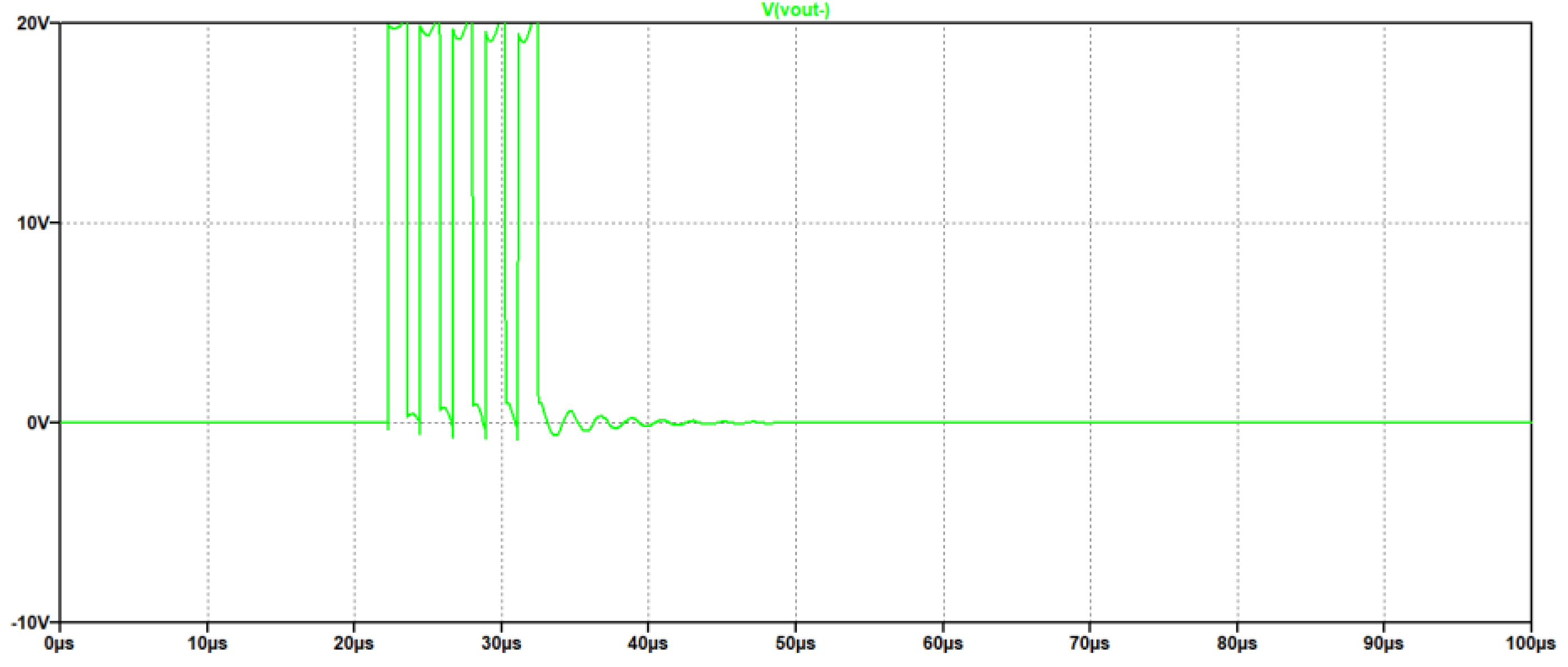
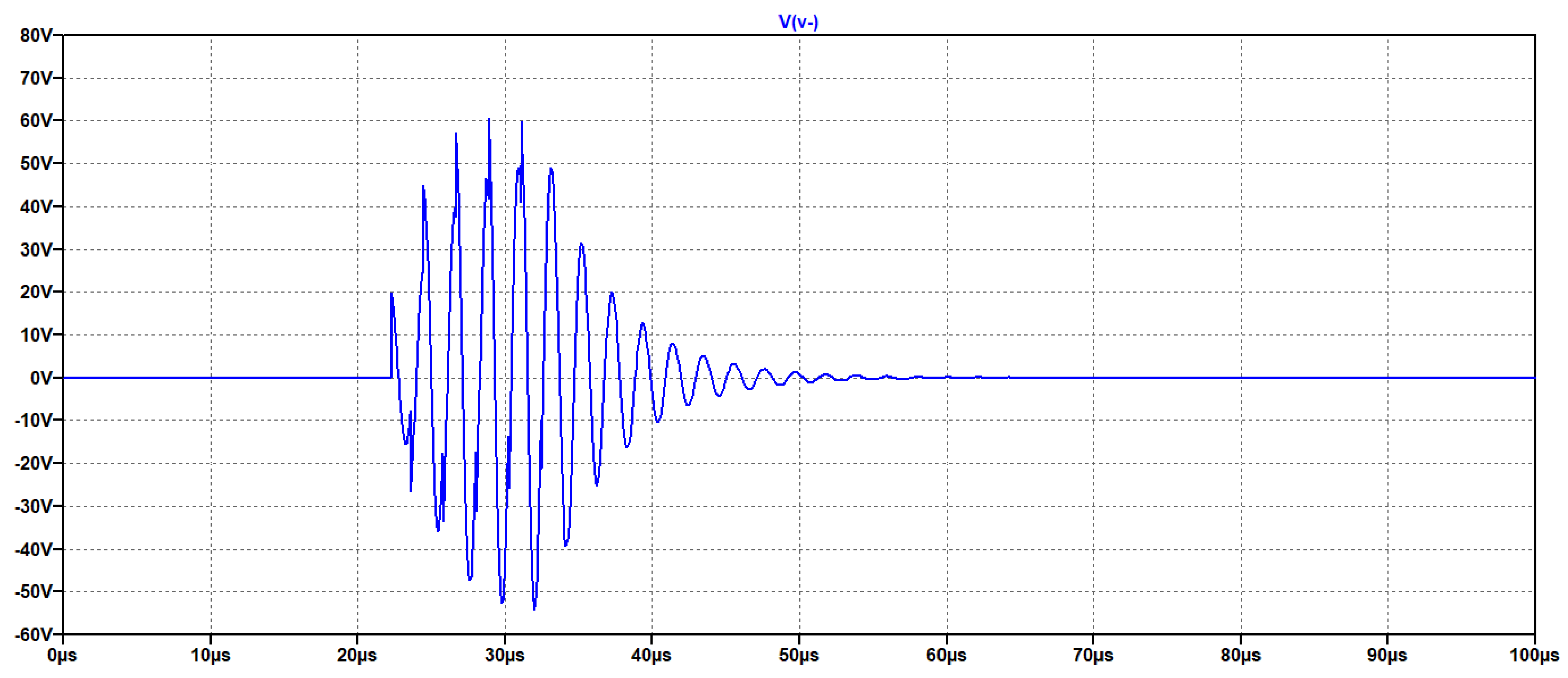
Figure 15.
(top) Excitation burst applied to one input of the differential matching network shown in Fig,.13 (Bottom) Output signal applied to one section of the UGWIDT.
Figure 15.
(top) Excitation burst applied to one input of the differential matching network shown in Fig,.13 (Bottom) Output signal applied to one section of the UGWIDT.

Table 1.
| | @ f=450 kHz.
| Ca | || | G |
| 600 pF | 1,62 | 2,85 |
| 700 pF | 2.57 | 3,33 |
| 800 pF | 4.27 | 3,80 |
| 900pF | 7.6 | 4,20 |
| 1000pF | 8.79 | 4,76 |
Table 2.
Vout @450 kHz.
| Rs [Ω] | Vout [Volt] |
| 0.4 | 133.2 |
| 1 | 129.6 |
| 4 | 121.5 |
Disclaimer/Publisher’s Note: The statements, opinions and data contained in all publications are solely those of the individual author(s) and contributor(s) and not of MDPI and/or the editor(s). MDPI and/or the editor(s) disclaim responsibility for any injury to people or property resulting from any ideas, methods, instructions or products referred to in the content. |
© 2025 by the authors. Licensee MDPI, Basel, Switzerland. This article is an open access article distributed under the terms and conditions of the Creative Commons Attribution (CC BY) license (http://creativecommons.org/licenses/by/4.0/).
Copyright: This open access article is published under a Creative Commons CC BY 4.0 license, which permit the free download, distribution, and reuse, provided that the author and preprint are cited in any reuse.


