
Submitted:
19 August 2025
Posted:
20 August 2025
You are already at the latest version
Abstract
The synthesis of bismuth(III) sulphide thin films on various textiles is of interest due to their potential applications in flexible solar absorber coatings and thin-film solar cells. These thin films were formed simultaneously on textiles of different compositions and morphologies using the environmentally friendly, low-cost successive ionic layer adsorption and reaction (SILAR) method at ambient temperature. The deposited films were characterised using X-ray diffraction (XRD), scanning electron microscopy (SEM), energy dispersive X-ray (EDX) spectroscopy, and ultraviolet-visible (UV-Vis) diffuse reflectance spectroscopy. This paper discusses how the structure and composition of the textiles affect the phase and elemental composition, crystallinity, morphology and optical properties of the formed films. The properties of the films are then compared. Depending on the textiles used, the formed films can be amorphous or semi-crystalline, and can be rich in sulphur or near to stoichiometric. Accordingly, the normalised atomic percentages of Bi in the films range from 3.62% to 33.87%, and those of S range from 96.38% to 66.13%. The energy band gap value of the composites also varies depending on the textile substrate, ranging from Eg = 1.58 eV to Eg = 1.8 eV. These properties directly impact the films' applications.
Keywords:
bismuth(III) sulphide films
; structural textile
; SILAR
; SEM
; optical properties
1. Introduction
Solar photovoltaic (PV) systems are supplying an increasing share of the global electricity market and the number of new installations is growing. Most of them use conventional crystalline silicon solar cells (SCs), which are rigid and brittle, and the processing of the silicon is a very expensive and complex process. Other perovskites photoelectrochemical solar cells (SEs), which have been extensively studied, are characterised by simplicity of design, but have drawbacks related to the cost and instability of the organic semiconductors used for charge transfer. In addition, this type of PV system is not suitable when a lightweight and flexible PV generator is required. The idea of creating a textile-based flexible PV system was inspired by the excellent performance of textiles in electronic devices. The selection of suitable textiles and semiconductors for alternative flexible photovoltaic structures is essential to meet these requirements.
Currently, various textiles are being used: polytetrafluoroethylene (PTFE) coated glass fiber (GF), mesh or aramid fabric, silicone coated fiberglass fabric, polyvinylchloride (PVC) coated polyester (PES) fabric etc. PTFE coated aramid fabric is a composite material that combines the high-performance characteristics of aramid fibers with the non-stick and heat-resistant properties of PTFE coating. This combination results in a fabric suitable for a wide range of industrial applications where strength and heat resistance properties are essential. Silicone coated fiberglass fabric is made of E-Glass fiberglass base fabric and high purity silicone coating. Electrically conductive textiles are made from woven or knitted conductive yarns. Surfaces can be sewn or embroidered with conductive threads or treated to impart conductivity. This can be achieved by applying a chemical coating or by using silver, nickel or copper nanoparticles for surface metallisation. It is a conductive fabric. Its electrical resistance is less than 1 Ω/sq [1].
Semiconductor thin films are being explored for application on textiles to create smart, functional building materials. These thin films, deposited on fabrics like polyester or cotton, can offer properties like increased durability, conductivity, or enhanced energy efficiency. Nanocrystalline semiconductors are of great interest to scientists due to their many applications in advanced electronic and optoelectronic devices. Metal sulphides are a particularly attractive group of functional materials due to their wide range of applications in electronics, energy storage and conversion, optics, electrochemical detection, photocatalysis and biomedicine [2,3,4,5]. This is thanks to their unique structural and optical properties.
Bismuth(III) sulphide (Bi₂S₃) is one of the non-toxic most promising semiconductor materials used in a variety of applications, including photovoltaic converters, photo-catalysts [6], thermoelectric cooling technologies based on the Peltier effect [7], hydrogen storage [8], as thermoelectric gas sensors [9,10], optical detection for IR and UV light [11,12], photoelectrochemical solar cells (SEs), and electronic and optoelectronic devices [7], furthermore, the Bi2S3 thin films can be used as efficient anode materials for lithium-ion batteries [13], or memristors [14], and even for cancer diagnostics [15,16]. It is an n-type crystalline semiconductor with several intrinsic properties, including a low direct energy band gap of 1.3−1.7 eV, which falls within the optimal range of the solar spectrum. It also has a high absorption coefficient of approximately 10⁴–10⁵ cm−1, high ionic conductivity and sufficient conversion efficiency of incident photons to electrons (∼5%) [17], making it an ideal candidate for solar energy conversion devices [18]. Bi2S3 has an orthorhombic, layered (lamellar) structure that is held together by weak Bi–S bonds. Some examples of bismuth sulphide nanostructures include belts, stars, spheres, ribbons, snowflakes, flowers, rods, tubes, and wires [19,20,21,22,23]. This van der Waals material has potential as a solar absorber, and its use in optoelectronics is the subject of extensive research [24].
There are several methods of depositing thin Bi₂S₃ films, such as thermal evaporation [25], chemical vapor deposition [26], solvothermal synthesis [27], the ultrasonic method [28], pulsed laser deposition [29], microwave irradiation [22], spray pyrolysis [30], electrodeposition [31]. However, the above methods of forming Bi₂S₃ thin films have several disadvantages, including the requirement for high temperatures and ultrahigh vacuums, which necessitate sophisticated equipment and are costly. Chemical methods, such as chemical bath deposition (CBD) [32] and successive ion layer adsorption and reaction (SILAR) [33], are very promising due to their user-friendly equipment, low deposition cost, and ability to deposit over a large surface area. The most important advantage of these methods, however, is the ability to control the reaction rate and film thickness. Bismuth nitrate pentahydrate is the predominantly used cationic precursor in both CBD and SILAR for bismuth containing thin film fabrication [32,33]. Sulphur-containing precursors such as thiourea, thiosulphate, thioacetamide [34], hydrogen sulphide [7], sodium sulphide and elemental sulphur are commonly used in the synthesis of bismuth sulphide by chemical methods [35]. In CBD film formation, the substrate and all cationic and anionic precursors are in the same reaction bath; therefore, the deposited materials adhere to both the substrate and the bath. In contrast, the SILAR method involves immersing the substrate in cationic and anionic precursors in different reaction baths. The absence of a complexing agent results in highly pure films. The outcome of this process is the deposition of thin films exclusively on the substrate. This constitutes one deposition cycle. The deposition rate can be controlled by adjusting the concentration of the precursor solutions. Film thickness can be controlled by varying the immersion time and the number of cycles. This enables simultaneous control of film deposition. In this study, the SILAR method was chosen to form thin Bi₂S₃ films.
The study aimed to form thin Bi₂S₃ films simultaneously on various textile materials using the SILAR method, and to evaluate the influence of the textile’s composition on the resulting composites surface phase composition, morphology, and optical properties.
2. Materials and Methods
2.1. Materials
For the deposition of bismuth sulphide thin films, 5 samples of textiles with different compositions were selected: polyethylene terephthalate fabric coated with polyvinyl chloride (PET/PVC, Verseidag-Indutex GmbH, Germany), glass fibre fabric coated with polytetrafluoroethylene (GF/PTFE, Verseidag-Indutex GmbH, Germany), cotton/polyester/spandex (C/PES/S, Mianyang Jialian Printing and Dyeing Co. Ltd., China), polyamide/silver (PA/Ag, Kufner Holding GmbH, Germany) and polyamide/copper (PA/Cu, Kufner Holding GmbH, Germany). The textile samples were cut into (2 × 7) cm2 samples. Table 1 lists the composition of each textile sample, along with photographs and the technical data provided by the manufacturer.
The following reagents were used to prepare the etching solutions: chromium(VI) oxide (CrO3, ≥97 wt%, Sigma-Aldrich Chemie GmbH, Germany), sulphuric acid (H2SO4, ≥96 wt%, Barta a Cihlar, Czech Republic) and orthophosphoric acid (H3PO4, ≥60 wt%, Lach-Ner, Ltd., Czech Republic). Bismuth nitrate (Bi(NO3)3·5H2O, ≥99 wt%, Sigma-Aldrich Chemie GmbH, Germany) and sodium thiosulphate (Na2S3O3·5H2O, >98 wt%, Sigma-Aldrich Chemie GmbH, Germany) were used to prepare solutions for the deposition of bismuth sulphide thin films.
2.2. Deposition of the Bi2S3 Thin Films
The bismuth sulphide films were deposited using the SILAR method, which makes our technology simpler and cheaper. A series of experiments were carried out to investigate the effect of solution concentration, immersion time and number of cycles on the quality of the films. Solutions with a concentration of 0.02–0.1 M were investigated. The number of deposition cycles apparently has the greatest effect on film thickness, so for thin film deposition, immersion cycles were varied from 1 to 7. Finally, the samples were alternately immersed in solutions of 0.1 M Bi(NO3)3 and 0.1 M Na2S2O3 at room temperature and left undisturbed for 8 hours. After each immersion in the solution, the samples were washed with distilled water. This constituted one deposition cycle. The number of immersion cycles seemed to have the greatest effect on the film thickness, so the immersion cycles were varied. The uniformity of the deposited film and the quality of its adhesion were checked visually and with a strong jet of water. The highest quality and best adhesion of Bi2S3 films to the structural textile surface was achieved after seven cycles. The basic equation of the reaction can be described as follows:
If there is excess sodium thiosulfate, it acts as a reducing agent and provides the BiS:
After 7 deposition cycles, the colour of the samples changed, they became grey-black or black, and were covered with a visually uniform layer of deposited material.
2.3. Analytical Techniques
The changes in chemical structure and bond configuration on the surface of untreated and treated GF/PTFE and PET/PVC samples were analysed using attenuated total reflectance (ATR) Fourier-transform infrared (FTIR) spectroscopy. ATR-FTIR spectra were recorded in the wavenumber range 3500–600 cm−1. Spectra were recorded on a Perkin Elmer FTIR Spectrum GX spectrophotometer by averaging 64 scans with a wavenumber resolution of 1 cm−1 at room temperature.
X-ray diffraction (XRD) analysis was carried out on a Bruker Advance D8 diffractometer with a tube voltage of 40 kV and a tube emission current of 40 mA. The X-ray beam was filtered with a Ni 0.02 mm filter to select CuKα (λ = 0.15406 nm) radiation. Diffraction patterns were recorded in a Bragg-Brentano geometry by using a fast-counting detector Bruker LynxEye based on the silicon strip technology. The specimens of the samples were scanned over the range of 2θ = 3–70° at a scan rate of 0.02°min−1 by using the coupled two theta/theta scan type.
The morphology and elemental analysis were investigated by scanning electron microscopy equipped with an energy dispersive X-ray spectroscopy detector (SEM-EDX). For SEM images, the samples were cut into smaller sizes of approximately 5 × 5 mm and coated with gold (Au) prior to morphological observation. SEM, observation of the samples was performed on a ZEISS EVO MA10 microscope at an accelerating voltage of 20 kV. The Bruker AXSX Flash 6/10 detector can detect all the elements present in the sample with an overall accuracy of about 1% and a detection sensitivity down to 0.1% by weight. A Lambda 35 UV-Vis spectrophotometer was used to record the UV-Vis diffuse reflectance spectra of the structural textile and the resulting composites in the 400–800 nm spectral range. The Kubelka–Munk method was used to determine the band gap (Eg) from the UV-Vis diffuse reflectance spectrum using the following equations [36,37]:
where F is the Kubelka–Munk function, R is the reflectance, hν is the photon energy, and Eg is the band gap, n is a constant denoting the power factor of the transition mode. For the allowed direct and indirect transitions, n = 2 and 1/2, respectively.
3. Results and Discussion
3.1. Thermo-Oxidative Acid Treatment of GF/PTFE and PET/PVC Samples
The surfaces of the GF/PTFE and PET/PVC samples were found to be hydrophobic, so the samples had to be chemically treated to improve their hydrophilicity and adhesion properties. The type of polymer, treatment time and temperature affect the process results such as roughness parameters, etching depth and appearance of hydrophilic groups, so it is important to select the appropriate etching solution and optimum etching conditions. In order to improve the etching results prior to the treatment, the GF/PTFE and PET/PVC samples were mechanically ground with SiO2 paper (p80 and p180 grit). The samples were then washed with hot running water and then with distilled water. This removed any dirt, dust, abrasive and broken particles adhering to the surface.
A thermo-oxidative acid treatment was chosen based on literature analysis and our experience [38]. The composition of the etching solution and the etching conditions are given in Table 2.
Although the GF/PTFE fabric is heat resistant up to 260 °C, an etching process at around 100 °C was chosen to reduce the overall risk of the process. The PET/PVC fabric was heat resistant to 70 °C, so the treatment was carried out at around 68 °C. Experiments were performed to determine the treatment time. At the end of the thermochemical treatment, the substrates were washed with hot running water, then rinsed with distilled water until the pH of the water reached a value of 7, and then air dried at room temperature. The samples were then stored in a desiccator containing CaCl2.
3.1.1. ATR-FTIR Spectroscopy of GF/PTFE and PET/PVC Samples
To better understand the changes in surface functional groups before and after chemical etching, the samples were analysed by ATR-FTIR spectroscopy. Figure 1 and Figure 2 show the ATR-FTIR spectra of the untreated and etched GF/PTFE and PET/PVC samples.
Figure 1 illustrates the ATR-FTIR spectra of the GF/PTFE samples before and after etching. According to the literature [39], the most intense bands observed at 1145 cm−1 and 1203 cm‒1 correspond to strong absorption of the valence symmetric and asymmetric stretching of CF2, while the C-C vibration band appears as a curvature around 1250 cm−1. The peaks observed at 640 cm−1, 553 cm−1 and 507 cm−1 correspond to CF2 deformation, CF2 wagging and CF2 twisting, respectively, and undergo intense changes simultaneously with the degree of crystallinity of PTFE [40]. The strong peaks at 1093 and 798 cm−1 is associated with asymmetric and symmetric Si-O-Si stretching vibrational bonding of glass fibre fabric [41]. However, the characteristic peak at 1093 cm−1 of the Si-O-Si band is in the same region as the stretching of CF2, resulting in an overlap of the peaks.
To understand structural changes in etched surface, x axis was magnified (Figure 1, inset). New functional groups appear in the ATR-FTIR reflectance spectrum of etched GF/PTFE sample surface (inset in Figure 1, spectrum 2). The peak at 3675 cm−1 is attributed to the valence vibrations of the -OH bond. The observed peaks at 2998 cm−1, 2900 cm−1 and 1409 cm–1 are assigned to valence asymmetric and valence symmetric C-H and valence C=C bond vibrations, respectively. The unsaturated vibration of the C-F bond is fixed at 925 cm–1.
Figure 2 shows the ATR-FTIR spectra of an untreated and an etched PET/PVC samples surface. The coexistence of different types of functional groups in PET/PVC has a combined effect and, as a result, the positions of the infrared absorption peaks are different from those reported in the published data for the pure form. The ester group in PET/PVC textile is confirmed by an intense >C=O stretching vibration mode at 1725 cm−1, stretching vibrations of C=O bond at 1192 cm−1, band at 1148 cm−1 corresponding to asymmetric stretching vibrations of O-C-C group and a very weak absorption peak at 1040 cm−1 resulting from C-O-C stretching vibrations [42,43,44]. The group of small vibrations in the spectral region from 2950 cm−1 to 2860 cm−1 could be attributed to the superposition of C-H stretching vibrations of -CHCl, CH3 and -CH2 groups of esters and -CH2 groups in PVC. The C-H wagging and rocking vibrations of the methylene groups are reflected in the bands at 1435 cm−1 and 965 cm−1, respectively. The bands associated with the -CHCl functional group appear at 1380 cm−1, 1073 cm−1 and 693 cm−1 and correspond to the stretching vibrations of C-H, the skeletal vibration of -CHCl and the stretching vibrations of C-Cl, respectively. The appearance of an intense peak at 1274 cm−1 can be related to complex superposition of three vibrations such as C-H wagging in methylene groups of PVC chain, C-H bending vibrations of -CHCl moieties and C=O stretching vibrations of ester group. This peak is observed at higher wavenumbers compared to the spectral position of the three peaks discussed above in pure PVC and ester group of PET. Two weak absorption peaks at 1600 cm−1 and 1580 cm−1 are related to -C=C bond vibrations, while C-H out-of-plane bending vibrations of benzene rings are represented by peaks at 877 cm−1, 799 cm−1 and 745 cm−1 [42,45]. The minor peak at 841 cm−1 cans be attributed to CaCO3 acting as a filler [46]. As shown (Figure 3, spectrum 2) slight changes were observed in the ATR-FTIR spectra of the etched sample. All the peaks described for the untreated PET/PVC surface are slightly diminished or shifted. The minor peak attributed to CO32− disappear, while CaCO3 dissolves in acidic medium. The appearance of the broad band in the region from 3656 cm−1 to 3075 cm−1 accompanied by a small shoulder in the region from 2443 cm−1 to 2194 cm−1 confirms the formation of new -OH and/or -C-OH functional groups on the etched PET/PVC textile surface.
The ATR-FTIR spectra show a functionalized surface of GF/PTFE and PET/PVC samples after thermo-oxidative acid treatment with oxygen containing >C=O and -C-OH functional groups. The reactivity of the surface with these groups is much higher, while its hydrophilicity, and consequently the adhesion of deposited thin Bi2S3 semiconductor films, is increased.
3.2. Structural, Morphological and Optical Characterisation of Obtained Composites
A visual evaluation of the surface of the resulting composites revealed a significant colour change to dark brown or black, confirming the formation of a new phase on the surface of the textile samples (Figure 3).
XRD was used to carry out the phase composition characterisation of the obtained Bi₂S₃ thin films on the surface of different structural textiles. The surface morphology and elemental composition of the deposited films were evaluated using SEM-EDX spectroscopy. UV-Vis diffuse reflectance (DR) spectroscopy was used to characterize the optical properties of obtained composites. Information about the electronic transitions of the different orbitals of a solid is provided through the absorption spectra by the technique of UV-Vis DR spectroscopy, which indirectly measures the material's electronic structure [36]. It has been reported that UV-Vis DR spectroscopy is the best tool for evaluating the optical characteristics of textile fibres [47].
3.2.1. Characterisation of GF/PTFE/Bi-S Samples Samples
XRD analysis was performed to better understand the changes in the surface phase composition of the untreated and etched GF/PTFE samples, as well as the GF/PTFE/Bi-S composite. XRD diffractograms are shown in Figure 4. The XRD data was analysed in detail using a combination of data from the literature and JCPDS reference templates.
According to the literature [48], PTFE is characterized by one intense X-ray diffraction peak at 2θ = 18○ and 6 peaks of low intensity appearing at 2θ = 30○ to 70○. These peaks correspond to (100), (110), (200), (210), (300), (220) and (310) crystal planes. Analysing the obtained XRD data of the untreated GF/PTFE construction textile sample (Figure 4, diffractogram 1), the diffraction peaks at 2θ = 18.1○, 31.7○, 36.8○, 41.4○, 49.5○, 56.3○ and 66.1○ were recorded in the specified interval, which are attributed to crystalline PTFE (JCPDS: 47-2217). According to sources [49,50], a broad and low-intensity peak at 2θ = 15.7○ can be attributed to amorphous PTFE.
After etching, no significant changes were observed in the position of any of the characteristic peaks of untreated GF/PTFE (2θ = 18.1°, 31.6°, 36.7°, 41.4°, 49.3°, 56.4° and 66.1°, Figure 4, diffractogram 2), although the intensity of the peaks at 2θ = 18.1° and 31.6° increased. No new peaks appeared. This leads us to conclude that the phase composition of the etched GF/PTFE sample remained unchanged. A diffractogram similar to that of the etched GF/PTFE sample was obtained after Bi₂S₃ thin films were deposited (see Figure 4, diffractogram 3). As previously reported [51] chemically deposited Bi₂S₃ films are often amorphous or semicrystalline in their as-deposited state. SEM images (Figure 5, (b)) show that the GF/PTFE surface is covered with nanostar-shaped crystallites that are characteristic of the Bi₂S₃ nanostructure. Therefore, we scraped a deposited layer from a composite surface and analysed it using XRD. The presence of XRD peaks at 2θ = 28.45° and 31.57° in the scraped material indicates that it is semicrystalline (see Figure 4(c)). These peaks are attributed to the orthorhombic phase of Bi₂S₃, with the following crystallographic planes: (211) and (221) (JCPDS: 17-320). EDX spectra (Figure 6(c)) showed that the deposited film was rich in sulphur. However, no sulphur peaks were registered. These results lead us to conclude that the deposited film is much thinner than the substrate, so no new phases could be detected in the diffractogram.
Figure 5 shows SEM images of the GF/PTFE/Bi-S composite. Image (a) shows that the surface is uneven, with cracks separating smooth clusters of various sizes. Increased magnification (Figure 5, image b) reveals nanostar-shaped structures on the substrate surface, which are characteristic of the Bi₂S₃ nanostructure. The nanostar particles and their aggregates vary significantly in size, ranging from approximately 300 nm to around 1.2 µm.
The elemental distribution was analysed using energy-dispersive X-ray spectroscopy (EDX). Spatial and concentration distributions, of bismuth and sulphur, on GF/PTFE are shown in Figure 6. Spatial distribution shows clustered distribution of both elements. Yellow spots (bismuth) appear to form dense clusters; brighter white spots correspond to nanostar-shaped Bi2S3 structures visible in SEM analysis. Blue matrix (sulphur) surrounds these clusters, suggesting sulphur is more evenly distributed over the substrate. Image B shows small yellow-green spots scattered across darker background, confirming localized enrichment of certain elements. The surface shows heterogeneous concentration distribution, reinforcing the idea of nanostar-structured deposition rather than uniform layer. As can be seen from the representative EDX spectra presented in Figure 6 (c), the Bi and S peaks are clearly visible in the EDX spectra of the samples, alongside additional peaks due to the GF/PTFE substrate, the substrate holder used in the EDX instrument, or the Au coating applied prior to morphological observation. The inset in Figure 6 (c) shows the normalised atomic percentages of bismuth and sulphur. The atomic ratios of Bi and S vary within the respective ranges of 3.62% and 96.38%. This indicates a high excess of sulphur. The excess S in Bi₂S₃ films prepared using Na₂S₂O₃ may also be due to thiosulphate, since thiosulphate can decompose into elemental S in an acidic medium. [52]. This acidic medium is formed during the hydrolysis of Bi(NO₃)₃.
Figure 7(a) shows the reflectance values of the untreated and etched GF/PTFE textile and GF/PTFE/Bi-S composite in the UV–Vis region. PTFE, a key component of the textile, has an average reflectance of over 93% from 250 to 400 nm, reaching around 99% in the visible and near-infrared spectrum [53]. However, its high diffuse reflection decreases with increasing GF content in textiles. For the untreated GF/PTFE textile, the percentage reflectance increases gradually from 25% at 200 nm to 76% at 800 nm (Figure 7(a), spectrum 1), whereas for the etched textile, it increases gradually from 32% at 200 nm to 73% at the same wavelength (Figure 7(a), spectrum 2). Depositing Bi₂S₃ films influences the reflectance of the GF/PTFE/Bi-S composite. Reflectance plateaus at around 13% between 200 and 500 nm before steadily increasing to 36% at 800 nm (Figure 7(a), spectrum 3).
The Eg value was determined from the UV-Vis DR spectrum by applying the Kubelka–Munk method. The experimental data show a long straight-line section in the (hvF)² vs. hv chart (Figure 7(b)), whereas the (hvF)¹/² vs. hv plots exhibit no linear behaviour, ruling out the possibility of an indirect band gap. The intersection between the linear fit and the photon energy axis gives an Eg value of 1.8 eV (Figure 7(b)).
3.2.2. Characterization of PET/PVC/Bi-S Samples
The diffractogram patterns of the PET/PVC samples before and after thermochemical treatment, as well as the obtained composites, are shown in Figure 8. A combination of data from the literature and JCPDS reference templates was used to analyse the XRD data in detail.
The XRD diffractogram of the untreated sample (Figure 8, curve 1) shows a broad, weak characteristic peak of PVC at 2θ = 18.78°, corresponding to the (110) crystal plane (JCPDS: 64-1628). The PET peak is observed at 2θ = 23.07° (JCPDS: 50-2275), and the peak at 2θ = 25.78° can be attributed to both PET and PVC. The five characteristic peaks at 2θ = 29.49°, 39.49°, 43.38°, 47.69° and 48.63° correspond to the (104), (113), (202), (016) and (018) crystal planes of rhombohedral calcite (CaCO₃, JCPDS: 05-0586). Similarly, six characteristic peaks at 2θ = 27.50°, 36.14°, 41.28°, 54.38°, 56.83° and 69.23° correspond to the (110), (101), (200), (211), (220) and (301) crystal planes of the tetragonal rutile phase of titanium dioxide (TiO₂; JCPDS: 04-006-1890).
In general, no phase changes occur after thermochemical treatment. However, there is a clear variation in the diffraction peaks corresponding to the peaks of both the organic components and the inorganic filler (Figure 8, diffractogram 2). The broad, weak PVC characteristic peak at 2θ = 18.78° and the small PET peak at 2θ = 23.07° disappear. Following treatment, the intensity of all TiO₂ peaks decreases compared to the untreated sample, as do those corresponding to CaCO₃. This suggests that the crystalline quality of the inorganic fillers has been reduced. A decrease in the intensity of all XRD peaks in a sample compared to an untreated sample suggests a change in the material's crystallinity or composition. As no new phase was identified, this could be due to factors such as reduced crystal size, increased lattice strain or an increased concentration of amorphous phases. The reduced crystallinity of the samples appeared to hinder fiber agglomeration and facilitate the diffusion of precursor ions.
After the deposition of thin films, a series of new peaks appear (see Figure 8, diffractogram 3). As reported [54], prominent 2θ peaks for orthorhombic phase bismuthinite (Bi₂S₃) in XRD patterns are typically found at around 28.6° and 31.8°. However, the specific 2θ values and their corresponding intensities may differ slightly depending on the synthesis method used and the quality of the Bi₂S₃ crystal. Therefore, the peak at 2θ = 28.67° (211) is attributed to the orthorhombic phase of Bi₂S₃ (JCPDS: 17-320). Additional Bi₂S₃ peaks may be observed at 2θ = 25.32° (310), 47.05° (350), 52.02° (540) and 53.37° (061). The increased intensity of the peak at around 2θ = 48.63°, initially attributed to calcite, shows that it overlaps with an additional Bi₂S₃ peak at 2θ = 48.62° (060). Similarly, the increased intensity of the peak at around 2θ = 56.83°, initially attributed to rutile, shows that it overlaps with an additional Bi₂S₃ peak at 2θ = 56.53° (451). Peaks at 2θ values of 14.48° (210), 19.94° (120), 31.22° (-601), 37.76° (133), and 41.76° (-721) can be assigned to monoclinic sulphur (JCPDS 76-183). Similarly, to Bi2S3, the increased intensity of the peak at around 2θ = 29.49°, initially attributed to calcite, shows that it overlaps with an additional sulphur peak at 2θ = 29.32° (420).
Figure 9 shows SEM images of deposited Bi2S3 thin film onto PET/PVC. From image (a) it is concluded that the surface is even; no cracks or pores are visible. Higher magnification (image (b)) shows uniform nanosphere-shaped structures, that differ in size (individual spheres measuring 100 nm and agglomerates measuring 1.14 µm), with no gaps separating them. Higher magnification (image (b)) reveals uniform nanosphere-shaped structures of various sizes (individual spheres measuring 100 nm and agglomerates measuring 1.14 µm), which are closely packed with no gaps between them. It can be speculated that the films grew by forming separate groups of nanoparticles in specific locations, gradually covering the entire textile surface with each subsequent deposition cycle.
Elemental distribution was analysed using EDX. Spatial and concentration distributions, of bismuth and sulphur, on PET/PVC are shown in Figure 10. The distribution of Bi and S appears relatively uniform. There are no large agglomerations of Bi or S, the two elements seem co-localized throughout the surface of the substrate, although sulphur seems to more evenly spread out across the surface. Results suggest a homogeneous composition, consistent with a well-formed composite. Image (b) shows small yellow-green spots scattered across darker background, confirming localized enrichment of certain elements. While concentration distribution is relatively even, higher concentration in certain areas suggests influxes that might attribute to larger nanostructures.
As can be seen from the results presented in Figure 10 (c), the Bi and S peaks are clearly visible in the EDX spectra of the samples, alongside additional peaks due to the PET/PVC substrate, its fillers, the substrate holder used in the EDX instrument, or the Au coating applied prior to morphological observation. The inset in Figure 10 (c) shows the normalised atomic percentages of bismuth and sulphur. The atomic ratios of Bi and S vary within the respective ranges of 4.19% and 95.81%. This indicates a high excess of sulphur and obtained results is in good agreement with XRD data.
Figure 11 shows the UV–Vis DR spectra of the untreated and etched PET/PVC samples, as well as the PET/PVC/Bi-S composite. PET fibres, which have a structure based on aromatic components, exhibit strong absorption of shorter ultraviolet wavelengths [55]. PVC is reported to exhibit absorption maxima at 280 and 245 nm in the UV region due to π–π* electronic transitions in the polymer backbone [56]. However, the PET/PVC textile used in this study exhibits a sharp absorption profile beyond 430 nm and minimal reflectance at 330 nm. This UV-Vis absorption profile is similar to that of CaCO₃/TiO₂ hybrid particles [57], which are utilised commercially. XRD analysis has revealed that the PET/PVC textile contains well-dispersed microparticles of CaCO₃ and TiO₂ acting as fillers. The polymer industry commonly employs TiO₂ in two capacities: as a white pigment and a UV-blocking additive. The primary function of these two applications is to prevent polymer degradation caused by UV exposure. TiO₂ is also a photocatalyst, which makes it perfect for use in self-cleaning coatings on different materials [58]. The reflectance intensity of the untreated PET/PVC sample in the 200–360 nm range is about 10–20%. Then, at 360 nm, it increases sharply, reaching 100% at 430 nm. Reflectance then gradually decreases, reaching 86% at 800 nm (Figure 11, spectrum 1). In the spectrum of the etched PET/PVC sample (see Figure 11, spectrum 2), a red shift was observed in the region of high absorption up to 370 nm due to the incorporation of functional groups in the PVC matrix. Within the 200–370 nm spectral range, the reflectance intensity of the etched PET/PVC sample is around 7–13%. Then, from 370 to 430 nm, this value increases sharply to 60%, continuing to rise until it reaches a nearly constant value of around 75–79% at 800 nm. Two additional broad absorption peaks were observed at 430 and 635 nm, which are associated with the functionalised surface. Within the 200–635 nm wavelength range, the PET/PVC/Bi-S composite's reflectance reaches a value of around 7% (see Figure 11, spectrum 3). This then increases monotonically to 24% at 800 nm. This composite demonstrates very good sunlight absorption.
An Eg value of 1.68 eV for the PET/PVC/Bi-S composite is given by the intersection between the linear fit and the photon energy axis (Figure 11, (b)).
3.2.3. Characterization of C/PES/S/Bi-S Samples
XRD was performed to obtain further information on the crystalline structure of the C/PES/S samples and the obtained composites (Figure 12). The XRD pattern of cellulose I, which is found within the cotton fibres, peaks are typically observed at the following 2θ angles: 15.2°, 16.7° and 23.1° (JCPDS: 03-0226). The diffraction patterns of the C/PES/S samples exhibited the peaks at 2θ = 15.01°, 16.67°, 22.99° and 34.23°, corresponding to the crystal lattice planes 110, 200, 220 and 004 of cellulose [54,59]. In the C/PES/S/Bi-S composite, the intensity of these peaks decreased and shifted to 2θ = 14.42°, 16.20°, and 22.66° compared to the initial sample. The peak at 34.23° disappeared. This suggests that the crystalline structure of cellulose changes after deposition of Bi₂S₃ films. Besides new peaks appeared at 2θ = 25.05°° (310), 28.43° (211), 31.61° (221) and 46.57° (501), which belong to the orthorhombic phase of Bi2S3 (JCPDS: 17-320). No sulphur peaks were detected.
Figure 13 shows SEM images of deposited Bi2S3 thin film onto C/PES/S. Image (a) shows that the deposited Bi₂S₃ coated the individual strands of material evenly. Figure 13, image (b) reveals an unorganised variety of differently shaped structures, including nanoflakes and nanoflowers. No cracks or pores are visible. The varying shapes are likely to have formed due to the uneven C/PES/S surface.
Spatial and concentration distributions, of bismuth and sulphur, on C/PES/S are shown in Figure 14. Spatial distribution (Figure 14 (a) shows an equal distribution of both bismuth and sulphur; no large clusters of either element are visible. Image (b) (Figure 14) shows a moderately large concentration of elements – which suggest large nanostructures with some lower concentration zones indicating smaller ones. These results confirm formation of smaller nanoflakes and larger nanoflowers. As can be seen from Figure 14(c), the EDX spectra of the samples clearly show peaks of bismuth (Bi) and sulphur (S), as well as additional peaks resulting from the substrate, the substrate holder used in the EDX instrument or the gold (Au) coating applied before morphological observation. The inset in Figure 14(c) shows the normalised atomic percentages of Bi and S. The atomic ratios of Bi and S vary within the respective ranges of 33.87% and 66.13%. The results obtained indicate a slight excess of amorphous sulphur (no S peaks were detected) and are in good agreement with the XRD data. It was reported [60,61] that atomic percentages of 40% Bi and 60% S in Bi₂S₃ films indicate stoichiometry. This suggests that the films formed on the C/PES/S substrate have a bismuth-to-sulfur molar ratio approaching that of the Bi₂S₃ compound.
Diffuse reflectance spectra were recorded to measure the amount of light reflected by a sample across the ultraviolet and visible light spectrums. Cotton generally reflects a significant portion of visible light. Its reflectance spectrum shows a gradual increase with increasing wavelength, reaching a plateau in the visible region. Its reflectance in the UV region (wavelengths below 400 nm) is particularly useful for distinguishing it from other textile fibres, such as viscose, bamboo, modal and Tencel, which tend to have a higher reflectance in this region [62]. The way light is reflected by cotton changes as its colour changes. In our study, the C/PES/S samples were coloured green/yellow. As these samples are a blend of three types of material (cotton, polyester and spandex), their UV-Vis DRS spectra differ from those of pure cotton fibres (Figure 15, (a)).
Typically, UV-Vis absorption spectra of cellulose I show minimal absorbance in the visible region (380–700 nm), with a decrease as the wavelength increases. A peak in the UV region, usually around 270–283 nm, is often associated with impurities such as lignin. Reflectance minima (peaks of absorbance) at around 200 and 225 nm are typical of π→π* electronic transitions in CC double bonds in polymer chains. Cotton fabrics have some disadvantages, such as low ultraviolet blocking [62]. Therefore, textiles are treated with a UV stabiliser. A peak at 310 nm could indicate the presence of a UV stabilisers, which typically has a peak in the range of 290–315 nm [63]. As shown in Figure 15 (a), spectrum 2, the absorption of samples increases after deposition of Bi₂S₃ thin films, reaching about 92% in the ultraviolet and visible regions. The Eg value for the C/PES/S/Bi-S composite is 1.58 eV, as determined by the intersection of the linear fit and the photon energy axis (Figure 15, (b)). The C/PES/S/Bi-S composite also demonstrates great potential for use as a solar cell absorber component.
3.2.4. Characterization of PA/Cu/Bi-S Samples
The PA/Cu textile under investigation was manufactured by depositing a layer of copper nanoparticles on the surface of the PA6 fiber fabric. The crystalline structure of the PA/Cu samples and the obtained composites was investigated using XRD (see Figure 16). The diffraction patterns of the PA/Cu samples (Figure 16, diffractogram 1) exhibited two small peaks at 2θ = 20.15° and 23.41°, assigned to the crystal lattice planes 200 and 002/202 of the α-crystalline form of PA6 (JCPDS: 022-0700). Two intense peaks were observed at 2θ = 43.10° and 53.10°, corresponding to the 111 and 200 crystal lattice planes of metallic copper, respectively. These results are consistent with JCPDS: 003-1018.
Despite the color changing from copper-colored to black after thin films of Bi₂S₃ were deposited, the XRD patterns of the PA/Cu/Bi-S composite (Figure 16, diffractogram 2) did not detect any peaks assigned to the Bi₂S₃ phase, except for those assigned to PA6 of the untreated PA/Cu sample. The Cu peaks had disappeared. The absence of peaks is probably due to the formation of an amorphous phase or very small crystallites. The small size of these crystallites reduces the scattering power of the incident X-ray beam, resulting in the disappearance of peaks in the diffraction pattern.
Figure 17 shows SEM images of deposited Bi2S3 thin film onto PA/Cu. Bi2S3 coated the surface of PA/Cu individual strands. After further magnification it is visible that the thin film is not evenly deposited with some deficit areas. Structures formed vary in size (250 - 900 nm) and shape, including layer of fine nanostars and individual larger nanoflakes.
Spatial and concentration distributions, of bismuth and sulphur, on PA/Cu are shown in Figure 18. Spatial distribution (Figure 18 (a)) shows evenly spreadout sulphur layer that covers the surface with sparse spots of bismuth, some of them forming larger structures. This is supported by concentration distribution (Figure 18 (b)), as there are spots of higher concentration, surrounded by dark blue areas.
As can be seen from the representative EDX spectra (shown as an inset in Figure 18(c)), the normalised atomic percentages of bismuth and sulphur are 32.68% and 67.32%, respectively. These values are very close to those obtained for the C/PES/S/Bi-S samples and tend to approach stoichiometry.
The reflectance spectrum of nylon fabric can vary depending on factors such as the type of nylon, its surface treatment and whether it is coated or dyed. Nylon generally has high reflectivity in the near infrared (NIR) range, with untreated nylon reflecting up to 90% of NIR radiation. However, due to its chemical structure, which includes amide groups (N-H) and carbonyl groups (C=O), PA6 fabric can absorb UV radiation through electronic transitions. Absorption in the 270–300 nm region is common for molecules containing a C=O group, corresponding to an n→π* transition. Nylon typically absorbs UV radiation, particularly in the 290–315 nm range [64]. In the NIR region, the diffuse reflectance of copper thin films tends to increase with wavelengths above 600 nm. Thicker films generally exhibit higher reflectance [65]. The presence of copper additives in the PA/Cu textile sample indicates a change in its optical properties of neat PA6. Consequently, the sample exhibits an absorption maximum at 260 nm, with a reflectance of 9% (see Figure 19(a), spectrum 1). Reflectance then increases stepwise from 260 nm to 550 nm, reaching 18%. Further reflectance shows an even stronger increase, reaching 55% at 800 nm. This is lower than that of woven fabrics, where the yarns are often interwoven. As the studied PA/Cu textile is a knitted fabric, the pores between the yarns are generally larger, which suggests lower reflectance. After the deposition of a thin film of bismuth sulfide, the deposited materials covered the individual yarns and reduced the pores. Consequently, the reflectance in the region from 200 nm to 550 nm was approximately 10%, except for a slight increase to 13% at 260 nm (Figure 19(a), spectrum 2). In the spectral region beyond 550 nm, reflection slowly increases, reaching 27% at 800 nm. The Eg value for the PA/Cu/Bi-S composite is 1.68 eV, as shown in Figure 19, (b). This was determined by plotting the linear fit and the photon energy axis.
3.2.5. Characterization of PA/Ag/Bi-S Samples
The PA/Ag textile was produced by coating the surface of the PA6 fibre fabric with silver nanoparticles. The diffraction patterns of the PA/Ag samples (Figure 20, diffractogram 1) exhibited one peak at 2θ = 21.38°. Specifically, in JCPDS 12-923, this peak is attributed to the (001) crystal lattice plane of the γ-phase of PA6. Three additional peaks of different intensity were also registered at 2θ = 37.98°, 44.18° and 64.37°, which correspond to the 111, 200 and 220 face-centered cubic silver crystal lattice planes (JCPDS: 04-0783), respectively.
The XRD patterns of the PA/Ag/Bi-S composite (Figure 20, diffractogram 2) show a that all the initial peaks registered for the PA/Ag samples disappeared. Three broad peaks, with maxima at approximately 2θ = 15.6°, 30.9° and 41.2°, were registered on the diffractogram. As can be seen in Figure 21(a), the PA/Ag textile consists of yarns. It is elastic and has small holes called eyelets. It can therefore be assumed that, during the formation of bismuth sulphide, the precursor solutions penetrated the knitted fabric and the precipitated materials coated the yarns. The presence of these broad peaks indicates an absence of a defined crystal structure, with only short-range order present.
Figure 21 shows SEM images of a deposited Bi2S3 thin film on a PA/Ag textile. The film coated the individual yarns of fabric evenly, with no visible imperfections (Figure 21(a)). Figure 21, image (b) shows an evenly deposited layer consisting of differently shaped structures, including fine nanostars and larger nanoflakes (150–600 nm). Cracks or pores are not visible.
Spatial and concentration distributions of bismuth and sulphur, on PA/Ag obtained by EDX are shown in Figure 22. Spatial distribution (Figure 22 (a)) provides the information that sulphur is more evenly distributed and that bismuth forms either smaller or larger clusters that result in nanostructures of differing size and shape. Results are supported in image (b) in Figure 22 as there are areas indicating surplus of elements. Representative EDX spectra (see inset in Figure 22(c)) show the normalised atomic percentages of bismuth and sulphur to be 17.68% and 82.32% respectively. These differ from the results obtained for composites C/PES/S/Bi-S and PA/Cu/Bi-S, and demonstrate that the obtained films are rich in sulphur.
Figure 23 shows the UV–Vis DR spectra of the PA/Ag textile samples, as well as the PA/Ag/Bi-S composite. As mentioned above, nylon PA6 fabric has characteristic absorption peaks in the UV region, typically in the 290–315 nm range. Therefore, absorption peak at 295 nm we attribute to the PA6. The metallic grey colour of the sample, resembling silver, suggests a change in its optical properties. Depending on their size, shape and distribution in nanostructures, monodisperse silver nanoparticles have two absorption bands: a broad peak in the range of 420–430 nm and a shoulder at 580–590 nm [66]. Therefore, a broad absorption peak, with a maximum at 425 nm, can be attributed to a small quantity of silver nanoparticles.
As shown in Figure 23 spectrum 2, absorption of the samples increased after deposition of the Bi₂S₃ thin films, reaching approximately 95% in the 200–600 nm region. There was also an absorption decrease in the visible and near-infrared regions. At 800 nm, the absorption level was 85%. We determined the Eg value for the PA/Ag/Bi-S composite to be 1.6 eV by intersecting the linear fit with the photon energy axis (see Figure 23, (b)).
4. Conclusions
The main objective of this study was to synthesise Bi₂S₃ semiconductor thin films on various flexible textiles simultaneously using the SILAR method. In the absence of a complexing agent, Na₂S₂O₃ was used as the sulphur precursor. The influence of textile composition on the phase composition, surface morphology and optical properties of the deposited films was investigated. XRD data revealed that the as-formed films consisted of amorphous, short-range ordered, or semicrystalline orthorhombic Bi₂S₃ phases (JCPDS: 17-320), with or without a crystalline monoclinic sulphur (S8) phase (JCPDS: 83-2285), depending on the textile substrate used. The substrate had a strong influence on the crystal structure of the film. The interaction between the film and the substrate also plays a role. SEM analysis revealed that Bi₂S₃ films did not grow uniformly; rather, they formed individual agglomerates of nanoparticles at specific locations, gradually covering the entire textile surface with each subsequent deposition cycle. The resulting bismuth sulphide nanostructures depend on the textile used and can take the form of stars, spheres, snowflakes or flowers. EDX spectroscopy was used to confirm the distribution of bismuth (Bi) and sulphur (S) within the nanoparticles and agglomerates. These elements were found to be concentrated in the top layers of the films, with bismuth ranging from 3.62 to 33.87 atomic percent and sulphur ranging from 67.32 to 96.38 atomic percent. These elements may have been present at different concentrations in the textile matrix, whereas secondary electrons (SEs) typically originate from within a few nanometres of the sample surface [67]. Additionally, EDX analysis revealed elevated levels of sulphur in the Bi₂S₃ films on individual textile samples. In its monoclinic form, sulphur is not a constituent of standard PV cells. However, it can be used in combination with other materials to produce components for energy storage, which could potentially impact PV technology indirectly [68,69]. Optical characterisation revealed that the deposited films are direct band gap semiconductors, with a band gap energy ranging from 1.58 to 1.8 eV. Although the films on different substrates were deposited simultaneously, the resulting composites differ in composition and structure. Clearly, the substrate on which the bismuth sulfide film is deposited affects its crystallinity, morphology, and optical properties. Therefore, future research should focus on selecting suitable textiles to produce semiconductor films with an appropriate bandgap that do not require annealing, for use in manufacturing flexible photovoltaic materials.
Author Contributions
Conceptualization, V.K.; methodology, V.K. and V.S.; software, V.S.; formal analysis, V.S.; investigation, V.K.; data curation, V.K.; writing—original draft preparation, V.K.; supervision, V.K.; funding acquisition, V.K. All authors have read and agreed to the published version of the manuscript.
Funding
This research was funded by the Lithuanian Research Council through its funding of student research and internships. Grant no. S-ST-23-64.
Data Availability Statement
The original contributions presented in this study are included in the article. Further inquiries can be directed to the corresponding author(s).
Acknowledgments
The authors would like to thank student E. Skuodaite from the Kaunas University of Technology for her help with the experiments.
Conflicts of Interest
The authors declare no conflicts of interest.
References
- Ojstršek, A.; Plohl, O.; Gorgieva, S.; Kurečič, M.; Jančič, U.; Hribernik, S.; Fakin, D. Metallisation of textiles and protection of conductive layers: an overview of application techniques. Sensors 2021, 21, 3508. [Google Scholar] [CrossRef]
- Zhong, H.; Bai, Z.; Zou, B. Tuning the luminescence properties of colloidal I-III-VI semiconductor nanocrystals for optoelectronics and biotechnology applications. J. Phys. Chem. Lett. 2012, 3, 3167–3175. [Google Scholar] [CrossRef]
- Talapin, D.V.; Lee, J.S.; Kovalenko, M.V.; Shevchenko, E.V. Prospects of colloidal nanocrystals for electronic and optoelectronic applications, Chem. Rev. 2010, 110, 389–458. [Google Scholar] [CrossRef]
- Manimegalai, D.K.; Manikandan, A.; Moortheswaran, S.; Antony, S.A. One-pot microwave irradiation synthesis and characterization studies of nanocrystalline CdS photocatalysts. Adv. Sci. Eng. Med. 2015, 7, 722–727. [Google Scholar] [CrossRef]
- Manikandan, A.; Antony, S.A. A novel approach for the synthesis and characterization studies of Mn2+ -Doped CdS nano-crystals by a facile microwave-assisted combustion method. J. Supercond. Nov. Magnetism. 2014, 27, 2725–2733. [Google Scholar] [CrossRef]
- Renuka Devee, D.; Sivanesan, T.; Muthukrishnan, R.M.; Pourkodee, D.; Mohammed Yusuf Ansari, P.; Abdul Kader, S.M.; Raniani, R.A. A novel photocatalytic activity of Bi2S3 nanoparticles for pharmaceutical and organic pollution removal in water remediation. Chem. Phys. Impact 2024, 8, 100605. [Google Scholar] [CrossRef]
- Onwudiwe, D.C. , Nkwe, V.M. Morphological variations in Bi2S3 nanoparticles synthesized by using single source precursor. Heliyon 2020, 6, e04505. [Google Scholar] [CrossRef]
- Razavi, F.S.; Mahdi, M.A.; Ghanbari, D.; Dawi, E.A.; Abed, M.J.; Ganduh, S.H.; Jasmin, L.S.; Salavati-Niasari, M. Fabrication and design of four-component Bi2S3/CuFe2O4/Cu2O nanocomposite as new active materials for high performance electrochemical hydrogen storage application. J. Energy Storage 2024, 94, 113493. [Google Scholar] [CrossRef]
- Yu, Y.; Hu, Z.; Lien, S.Y.; Yu, Y.; Gao, P. Self-powered thermoelectric hydrogen sensors based on low-cost bismuth sulphide thin films: quick response at room temperature. ACS Appl. Mater. Interfaces 2022, 14, 47696–47705. [Google Scholar] [CrossRef]
- Kan, H.; Yang, W.; Guo, Z.; Li, M. Highly sensitive room-temperature NO2 gas sensor based on Bi2S3 nanorods. J. Mater. Sci. Mater. Electron. 2024, 35, 331. [Google Scholar] [CrossRef]
- Rong, P.; Gao, S.; Ren, S.; Lu, H.; Yan, J.; Li, L.; Zhang, M.; Han, Y.; Jiao, S.; Wang, J. Large-area freestanding Bi2S3 nanofibrous membranes for fast photoresponse flexible IR imaging photodetector. Adv. Funct. Mater. 2023, 33, 2300159. [Google Scholar] [CrossRef]
- Singh, A.; Chauhan, P.; Verma, A.; Yadav, B.C. Interfacial engineering enables polyaniline-decorated bismuth sulphide nanorods towards ultrafast metal-semiconductor-metal UV-Vis broad spectra photodetector. Adv. Compos. Hybrid Mater. 2024, 7, 88. [Google Scholar] [CrossRef]
- Zhang, X.; Xie, J.; Tang, Y.; Lu, Z.; Hu, J.; Wang, Y.; Cao, Y. Oxygen self-doping Bi2S3@C spheric successfully enhanced long-term performance in lithium-ion batteries. ACS Appl. Mater. Interfaces 2024, 16, 52423–52431. [Google Scholar] [CrossRef]
- Terdalkar, P.; Kumbhar, D.D.; Pawar, S.D.; Nirmal, K.A.; Kim, T.G.; Mukherjee, S.; Khot, K.V.; Dongale, T.D. Revealing switching statistics and artificial synaptic properties of Bi2S3 memristor. Solid State Electron. 2025, 225, 109076. [Google Scholar] [CrossRef]
- Zhao, Y.; Tao, Y.; Huang, Q.; Huang, J.; Kuang, J.; Gu, R.; Zeng, P.; Li, H.-Y.; Liang, H.; Liu, H. Electrochemical Biosensor Employing Bi2S3 Nanocrystals-Modified Electrode for Bladder Cancer Biomarker Detection. Chemosensors 2022, 10, 48. [Google Scholar] [CrossRef]
- Yang, Z.; Wang, L.; Zhang, J.; Liu, J.; Yu, X. Application of bismuth sulphide based nanomaterials in cancer diagnosis and treatment. Nano Today 2023, 49, 101799. [Google Scholar] [CrossRef]
- Liang, K.; Wang, C. Capacitive and photocatalytic performance of Bi2S3 nanostructures synthesized by solvothermal method. Phys. Lett. A 2017, 38, 652–657. [Google Scholar] [CrossRef]
- Supekar, A.T.; Bhujbal, P.K.; Salunke, S.A.; Rathod, S.M.; Patole, S.P.; Pathan, H.M. Bismuth sulphide and antimony sulphide-based solar cells: a review. ES Energy Environ. 2023, 19, 848. [Google Scholar] [CrossRef]
- Yu, X.L.; Cao, C.B. Photoresponse and field-emission properties of bismuth sulphide nanoflowers. Cryst. Growth & Design 2008, 8, 3951–3955. [Google Scholar] [CrossRef]
- Yu, Y.; Jin, C.H.; Wang, R.H. : Chen, Q.; Peng, L.M. High-quality ultralong Bi2S3 nanowires: structure, growth, and properties. J. Phys. Chem. 2005, 109, 18772–18776. [Google Scholar] [CrossRef] [PubMed]
- Ajiboye, T.O.; Onwudiwe, D.C. Bismuth sulphide based compounds: properties, synthesis and applications. results. Chem. 2021, 3, 100151. [Google Scholar] [CrossRef]
- Onwudiwe, D.C.; Ovewo, O.A.; Atamtürk, U.; Ojelere, M.S. Photocatalytic reduction of Cr(VI) using star-shaped Bi2S3 obtained from microwave irradiation of bismuth complex. J. Environ.Chem. Eng. 2020, 8, 103816. [Google Scholar] [CrossRef]
- Zhang, M.; Chen, D.J.; Wang, R.Z.; Feng, J.J.; Bai, Z.; Wang, A.J. D-penicillanime assited hydrothermal synthesis of Bi2S3 nanoflowers and their electrochemical application. Mater. Sci. Eng. 2013, 33, 3980–3985. [Google Scholar] [CrossRef] [PubMed]
- Linhart, W.M.; Zelewski, S.J.; Scharoch, P.; Dybała, F.; Kudrawiec, R. Nesting-like band gap in bismuth sulphide Bi2S3. J. Mater. Chem. C. 2021, 9, 13733–13738. [Google Scholar] [CrossRef]
- Ran, Y.; Song, Y.; Jia, X.; Gu, P.; Cheng, Z.; Zhu, Y.; Wang, Q.; Pan, Y.; Li, Y.; Gao, Y.; et al. Large-Scale Vertically Interconnected Complementary Field-Effect Transistors Based on Thermal Evaporation. Small 2024, 20, 2309953. [Google Scholar] [CrossRef] [PubMed]
- Atamturk, U.; Jung, E.; Fischer, T.; Mathur, S. Tale of Two Bismuth Alkylthiolate Precursors’ Bifurcating Paths in Chemical Vapor Deposition. Chem. Mater. 2022, 34, 7344–7356. [Google Scholar] [CrossRef]
- Tezcan, F. ; A new synthesis route of Bi2S3 with solvothermal deposition in photoelectrochemical hydrogen production, Jour. of Molec. Struct. 2024, 1301, 137418. [Google Scholar] [CrossRef]
- Parra-Arciniega, S.M.; Garcia-Gomez, N.A.; Garza-Toyar, L.L.; García-Gutiérrez, D.I.; Sánchez, E.M. Ultrasonic irradiation-assisted synthesis of Bi2S3 nanoparticles in aqueous ionic liquid at ambient condition. Ultrason. Sonochem. 2017, 36, 95–100. [Google Scholar] [CrossRef]
- Rodriguez-Rosales, K.; Cruz-Gomez, J.; Cruz, J.S.; Guillen-Cervantes, A.; de Moure-Flores, F.; Villagran-Muniz, M. Plasma emission spectroscopy for studying Bi2S3 produced by pulsed laser deposition and effects of substrate temperature on structural, morphological, and optical properties of thin films. Mater. Sci. Eng. B 2025, 312, 117867. [Google Scholar] [CrossRef]
- Bouachri, M.; Oubakalla, M.; El Farri, H.; Diaz-Guerra, C.; Mhalla, J.; Zimou, J.; El-Habib, A.; Beraich, M.; Nouneh, K.; Fahoume, M.; et al. Substrate temperature effects on the structural, morphological and optical properties of Bi2S3 thin films deposited by spray pyrolysis: An experimental and first-principles study. Opt. Mater. 2023, 135, 113215. [Google Scholar] [CrossRef]
- Grubač, Z.; Metikoš-Huković, M. Electrodeposition of thin sulphide films: nucleation and growth observed for Bi2S3. Thin solid films. 2002, 412, 248–256. [Google Scholar] [CrossRef]
- Castillo-Carillo, A.; Rivas-Valles, B.G.; Castillo, S.J.; Ramirez, M.M.; Luque-Morales, P.A. New formulation to synthesize semiconductor Bi2S3 thin films using chemical bath deposition for optoelectronic applications. Chem: Sym. 2022, 14, 2487. [Google Scholar] [CrossRef]
- Raut, S.S.; Dhobale, J.A.; Sankapal, B.R. SILAR deposited Bi2S3 thin film toward electrochemical supercapacitor. Physica E. 2017, 87, 209–212. [Google Scholar] [CrossRef]
- Selmane, N.; Eddine, H. Effect of complexing agent on the structural properties of bismuth sulphide Bi2S3 thins films prepared by chemical bath deposition technique. Revue des Sciences et Sciences de l’Ingénieur 2010, 1, 22–26. [Google Scholar]
- Fazal, T.; Iqbal, S.; Shah, M.; Ismail, B.; Shaheen, N.; Alharthi, A.I.; Awwad, N.S.; Ibrahium, H.A. Correlation between structural, morphological and optical properties of Bi2S3 thin films deposited by various aqueous and non-aqueous chemical bath deposition methods. Results Phys. 2022, 40, 105817. [Google Scholar] [CrossRef]
- López, R.; Gómez, R. Band-gap energy estimation from diffuse reflectance measurements on sol-gel and commercial TiO2: a comparative study. J. Sol-Gel Sci. Technol. 2012, 61, 1–7. [Google Scholar] [CrossRef]
- Nasr, M.; Viter, R.; Eid, C.; Warmont, F.; Habchi, R.; Miele, P.; Bechelany, M. Synthesis of novel ZnO/ZnAl2O4 multi co-centric nanotubes and their long-term stability in photocatalytic application. RSC Adv. 2016, 6, 103692–103699. [Google Scholar] [CrossRef]
- Alaburdaitė, R. , Krylova, V. Polypropylene film surface modification for improving its hydrophilicity for innovative applications. Polym. Degrad. Stab. 2023, 211, 110334–1. [Google Scholar] [CrossRef]
- Asrafali, S.P.; Periyasamy, T.; Kim, S.C. Hydrophilic Nature of Polytetrafluoroethylene through Modification with Perfluorosulfonic Acid-Based Polymers. Sustainability 2023, 15, 16479. [Google Scholar] [CrossRef]
- Pugmire, D.L.; Wetteland, C.J.; Duncan, W.S.; Lakis, R.E.; Schwartz, D.S. Cross-linking of polytetrafluoroethylene during room-temperature irradiation. Polym. Degrad. Stab. 2009, 94, 1533–1541. [Google Scholar] [CrossRef]
- Liu, Q.; Shi, J.; Sun, J.; Wang, T.; Zeng, L.; Jiang, G. Graphene and graphene oxide sheets supported on silica as versatile and high-performance adsorbents for solid-phase extraction. Angew. Chem. Int. Ed. 2011, 50, 5913–5917. [Google Scholar] [CrossRef] [PubMed]
- Krylova, V.; Dukštienė, N.; Lelis, M.; Tučkutė, S. : PES/PVC textile surface modification by thermo-chemical treatment for improving its hydrophilicity. Surfaces and Interfaces 2021, 25, 101184. [Google Scholar] [CrossRef]
- Xia, L.; Zhang, Q.; Zhuang, X.; Zhang, S.; Duan, C.; Wang, X.; Cheng., B. Hot-pressed wet-laid polyethylene terephthalate nonwoven as support for separation membranes. Polymers 2019, 11, 1547. [Google Scholar] [CrossRef] [PubMed]
- M. Kormunda, J. M. Kormunda, J. Pavlik, Characterization of oxygen and argon ion flux interaction with PET surfaces by in-situ XPS and ex-situ FTIR. Polym. Degrad. Stab 2010, 95, 1783–1788. [Google Scholar] [CrossRef]
- Zhang, H.; Li, X.; Mao, N.; Sun, R.; Xu, J. Fabrication of magnetized polyester fabric grafted with -cyclodextrin for controlled release of menthol. J. Ind. Text. 2016, 47, 1060–1082. [Google Scholar] [CrossRef]
- Moros, J.; Cassella, R.J.; Barciela-Alonso, M.C.; Moreda-Pineiro, A.; Herbello-Hermelo, P.; Bermejo-Barrera, P. Estuarine sediment quality assesment by Fourier-transform infrared spectroscopy. Vib. Spectrosc. 2010, 53, 204–213. [Google Scholar] [CrossRef]
- 50. Si, J.; Ma, R.; Wu, Y.; Dong, Y. 50. Si, J.; Ma, R.; Wu, Y.; Dong, Y. Microstructure and magnetic properties of novel powder cores composed of iron-based amorphous alloy and PTFE. J. Mater. Sci. 8154. [Google Scholar] [CrossRef]
- Hu, X.; Zhang, Q.; Yu, H.; Zhao, D.; Dong, S.; Zhou, Q. Quantitative analysis of naturally colored cotton and white cotton blends by UVvis diffuse reflectance spectroscopy. Jour. of Appl. Spect. 2015, 81, 949–955. [Google Scholar] [CrossRef]
- Shulga, Y.M.; Vasilets, V.N.; Kiryukhin, D.P.; Voylov, D.N. Polymer composites prepared by low-temperature post-irradiation polymerization of C2F4 in the presence of graphene-like material: synthesis and characterization. RCS Adv. 2015, 5, 9865–9874. [Google Scholar] [CrossRef]
- Miyase, A.; Qu, S.; Lo, K.H., Wang, S.S. Elevated- temperature thermal expansion of PTFE/PEEK matrix composite with random-oriented short carbon fibers and graphite flakes. Jour. of Eng. Mat. and Tech. Trans of the ASME. 2020, 142, 021002. [CrossRef]
- Rincón, M.E.; Campos, J.; Suárez, R. A comparison of the various thermal treatments of chemically deposited bismuth sulfide thin films and the effect on the structural and electrical properties. Journ. of Phys. and Chem. of Solids 1999, 60, 385–392. [CrossRef]
- Gao, C.; Shen, H.; Sun, L.; Shen, Z. Chemical bath deposition of Bi2S3 films by a novel deposition system. Appl. Surf. Science 2011, 257, 7529–7533. [CrossRef]
- Li, Z.; Si, G.; Ning, Z.; Liu, J.; Fang, Y.; Si, B.; Cheng, Z.; Yang, C. Highly Sensitive Sphere-Tube Coupled Photoacoustic Cell Suitable for Detection of a Variety of Trace Gases: NO2 as an Example. Sensors 2022, 22, 281. [CrossRef]
- Dutta, A.K.; Maji, S.K.; Mitra, K.; Sarkar, A.; Saha, N.; Ghosh, A.B.; Adhikary, B. Single source precursor approach to the synthesis of Bi2S3 nanoparticles: A new amperometric hydrogen peroxide biosensor. Sens. and Actuat.. B: Chem. 2024, 192, 578–585. [Google Scholar] [CrossRef]
- Achwal, W.B. Sun protection properties of textile substrates. Colorage 1997, 44, 31–31.
- Abdel-Fattah, E.; Alharthi, A.I.; Fahmy, T. Spectroscopic, optical and thermal characterization of polyvinyl chloride-based plasma-functionalized MWCNTs composite thin films. Appl. Phys. A. 2019, 125, 475. [Google Scholar] [CrossRef]
- Sun, S.; Ding, H.; Hou, X. Preparation of CaCO3-TiO2 composite particles and their pigment properties. Mater. 2018, 11, 1131. [Google Scholar] [CrossRef]
- da Silva, D.J.; Escote, M.T.; Cruz, S.A.; Simião, D.F.; Zenatti, A.; Curvello, M.S. Polycarbonate/TiO2 nanofibers nanocomposite: Preparation and properties. Polym. Compos. 2018, 39, 780–790. [Google Scholar] [CrossRef]
- Acharya, S.; Hu, Y.; Abidi, N. Cellulose Dissolution in Ionic Liquid under Mild Conditions: Effect of Hydrolysis and Temperature. Fibers 2021, 9, 5. [Google Scholar] [CrossRef]
- Riahi, M.; Martinez-Tomas, C.; Agouram, S.; Boukhachem, A.; Maghraoui-Meherzi, H. The effects of thermal treatment on structural morphological and optical properties of electrochemically deposited Bi2S3 thin films. Thin Solid Film 2017, 626, 9–16. [Google Scholar] [CrossRef]
- Sonawane, P.S.; Patil, L.A. Effect of nonstoichiometry on structural and optical properties of nanostructured Bi2S3 thin films prepared chemically at room temperature. Mater. Chem. Phys. 2007, 105, 157–161. [Google Scholar] [CrossRef]
- Goncalves, G.; Marques, P.A.; Pinto, R.J.; Trindade, T.; Neto, C.P. Surface modification of cellulosic fibres for multipurpose TiO2 based nanocomposites. Compos. Sci. Technol. 2009, 69, 7–8. [Google Scholar] [CrossRef]
- Bai, C.; Yuan, X.; Cao, Y.; Hao, Z.; Pan, L.; Peng, J.; Liu, N.; Chen, S. Perdurable antimicrobial and ultraviolet-blocking cotton fabric by one-step eco-friendly strategy. Industr. Crop. and Prod. 2025, 223, 120038. [Google Scholar] [CrossRef]
- Das, B.R. UV Radiation Protective Clothing. The Op. Text. Jour. 2010, 3, 14–21. [Google Scholar]
- Foadi, F.; Etminan, M.; Aghamir, F.M.; Mohammadizadeh, M.R. Role of surface morphological parameters on wettability of obliquely deposited Cu thin films in a plasma focus device. Jour. of Mater. Resear. 2023, 38, 3666–3676. [Google Scholar] [CrossRef]
- Singh, S.; Bharti, A.; Meena, V.K. Green synthesis of multi-shaped silver nanoparticles: Optical, morphological and antibacterial properties. J. Mater. Sci. Mater. Electron. 2015, 26, 3638–3648. [Google Scholar] [CrossRef]
- Fleck, N.; Amli, H.; Dhanak, V.; Ahmed, W. Chapter 11 - Characterization techniques in energy generation and storage. In Emerging Nanotechnologies for Renewable Energy, In Micro and Nano Technologies; Ahmed, W., Booth, M., Nourafkan, E., Eds.; Elsevier: Amsterdam, The Netherlands, 2021; pp. 259–285. ISBN 9780128213469. [Google Scholar] [CrossRef]
- Jung, S.C.; Han, Y.-K. Monoclinic sulfur cathode utilizing carbon for high-performance lithium-sulfur batteries. Jour. Pow. Sour. 2016, 325, 495–500. [Google Scholar] [CrossRef]
- Moon, S.; Jung, Y.H.; Jung, W.K.; Jung, D.S.; Choi, J.W.; Kim, D.K. Encapsulated Monoclinic Sulfur for Stable Cycling of Li–S Rechargeable Batteries. Adv. Mater. 2013, 25, 6547–6553. [Google Scholar] [CrossRef]
Figure 1.
ATR-FTIR spectra of GF/PTFE architectural textiles in the 4000–560 cm−1 wavenumber range: 1 – untreated, 2 – etched. The inset shows a magnified view of the x-axis.
Figure 1.
ATR-FTIR spectra of GF/PTFE architectural textiles in the 4000–560 cm−1 wavenumber range: 1 – untreated, 2 – etched. The inset shows a magnified view of the x-axis.
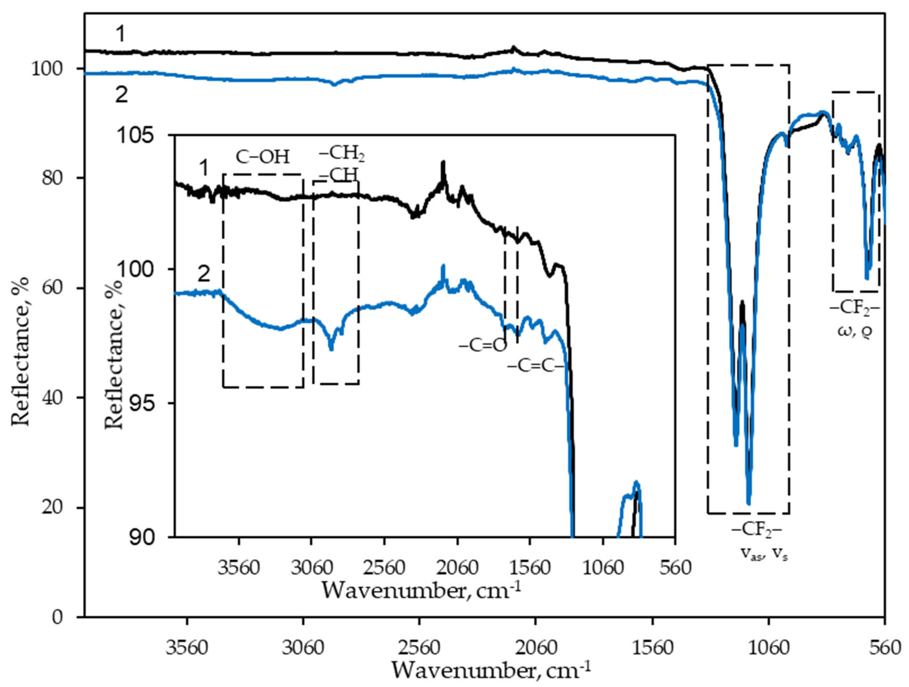
Figure 2.
ATR-FTIR spectra of PET/PVC structural textiles in the 4000−560 cm-1 wavenumber range: 1 – untreated; 2 – etched.
Figure 2.
ATR-FTIR spectra of PET/PVC structural textiles in the 4000−560 cm-1 wavenumber range: 1 – untreated; 2 – etched.
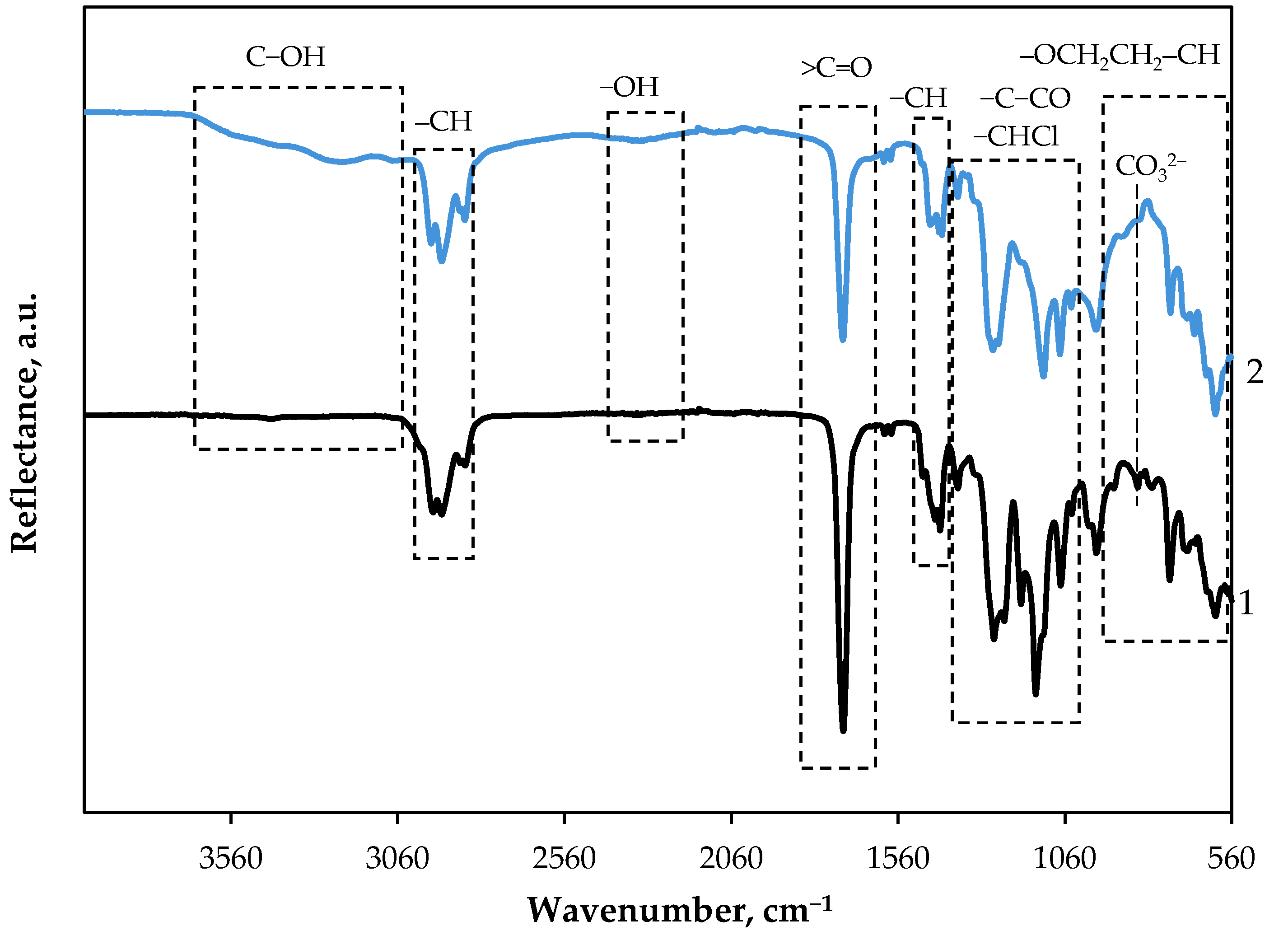
Figure 3.
Images of obtained composites: (a) – GF/PTFE/Bi-S; (b) – PET/PVC/Bi-S; (c) – C/PES/S/Bi-S; (d) – PA/Cu/Bi-S; (e) – PA/Ag/Bi-S.
Figure 3.
Images of obtained composites: (a) – GF/PTFE/Bi-S; (b) – PET/PVC/Bi-S; (c) – C/PES/S/Bi-S; (d) – PA/Cu/Bi-S; (e) – PA/Ag/Bi-S.
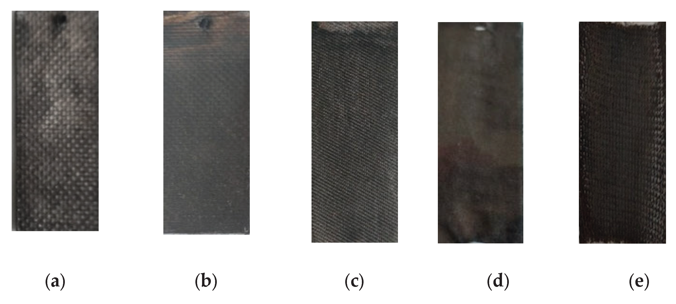
Figure 4.
XRD diffractogram of: 1 – untreated GF/PTFE sample; 2 – etched GF/PTFE sample; 3 – GF/PTFE/Bi-S composite. (a) – full range; (b) – zoomed-in view between 30 and 70 2θ.; (c) – scraping from a GF/PTFE/Bi-S composite surface.
Figure 4.
XRD diffractogram of: 1 – untreated GF/PTFE sample; 2 – etched GF/PTFE sample; 3 – GF/PTFE/Bi-S composite. (a) – full range; (b) – zoomed-in view between 30 and 70 2θ.; (c) – scraping from a GF/PTFE/Bi-S composite surface.
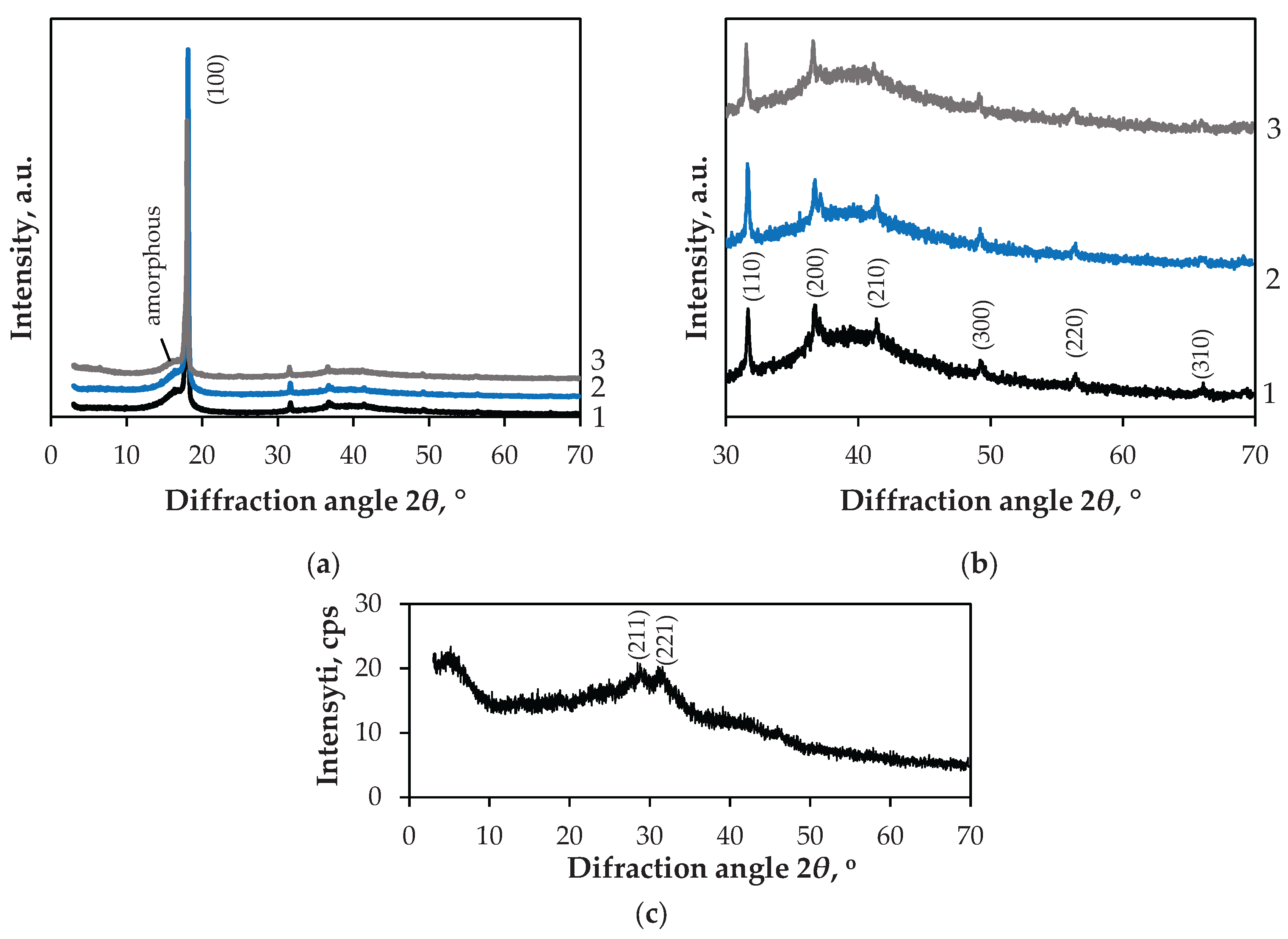
Figure 5.
SEM images of GF/PTFE/Bi-S composite: (a) – 300x magnified; (b) – 40000x magnified.
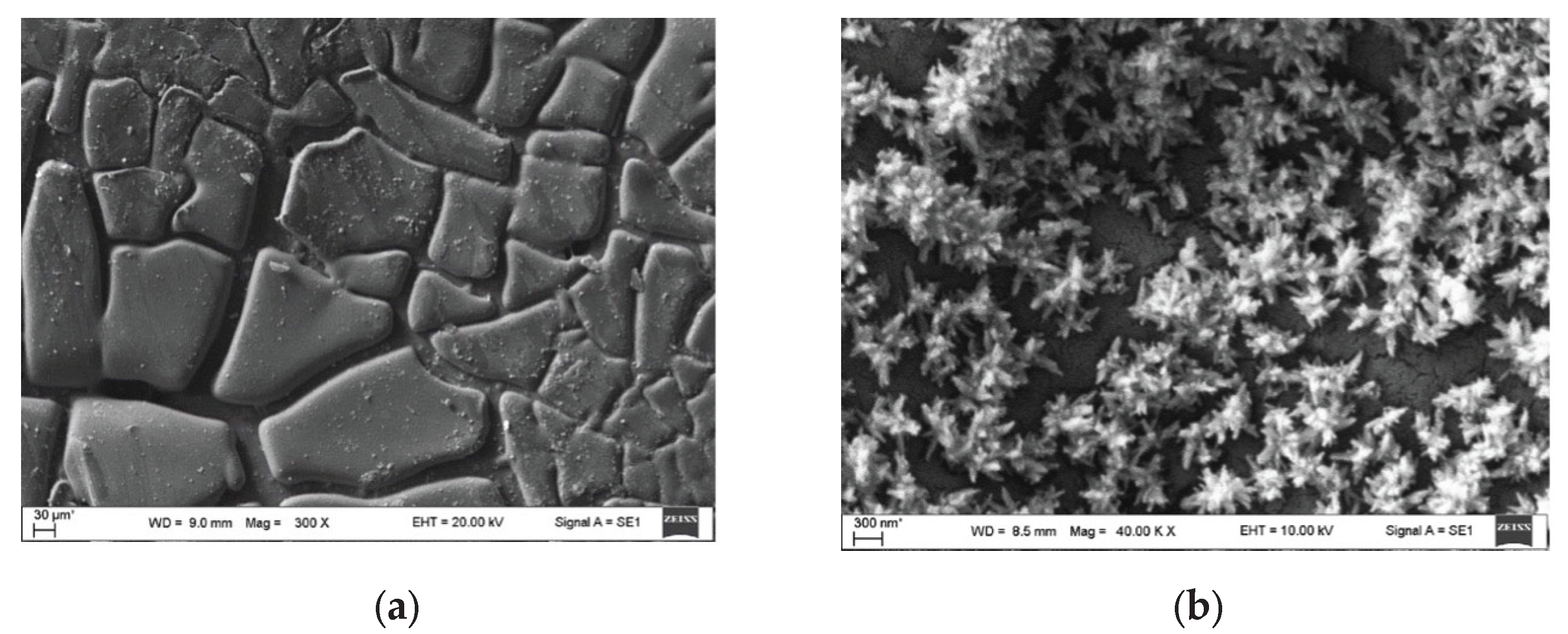
Figure 6.
EDX elemental maps of Bi (yellow) and sulphur (blue) (10000x magnified) of GF/PTFE/Bi-S surface: (a) – spatial distribution of elements; (b) – elemental concentration distribution; (c) – representative EDX spectra. The normalised atomic percentages of Bi and S in the films are shown in the corresponding inset.
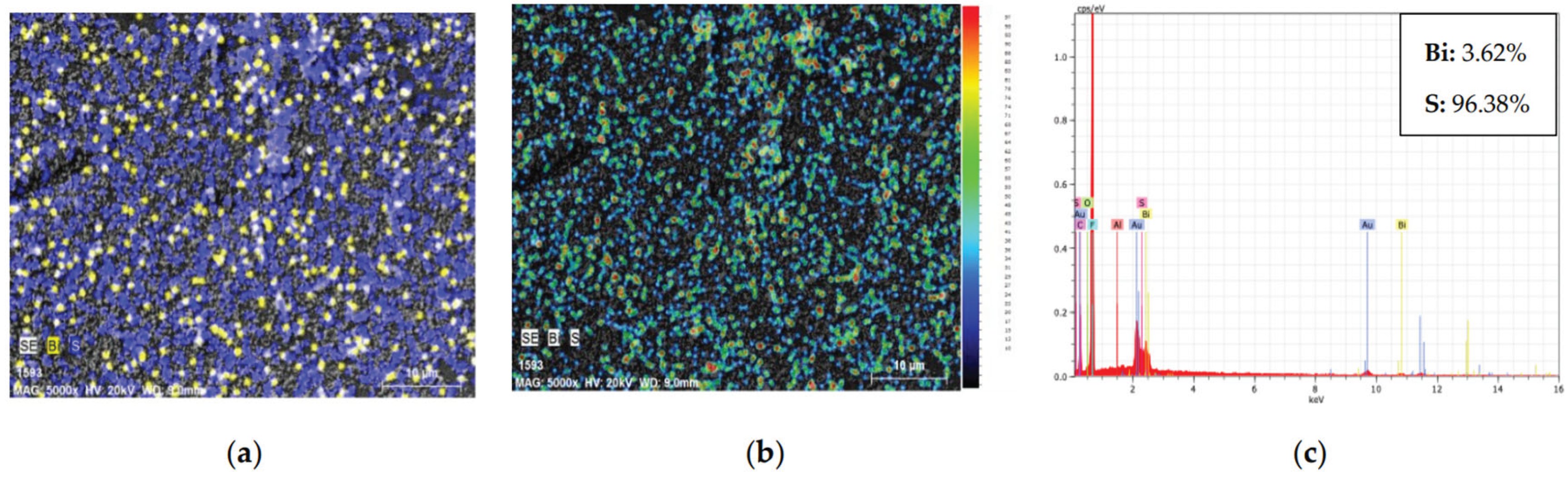
Figure 7.
(a) Optical reflectance spectra as a function of the wavelength in the range of 200–800 nm for: GF/PTFE; 2 – etched GF/PTFE; 3 – GF/PTFE/Bi-S composite; (b) Eg determination by Kubelka – Munk method.
Figure 7.
(a) Optical reflectance spectra as a function of the wavelength in the range of 200–800 nm for: GF/PTFE; 2 – etched GF/PTFE; 3 – GF/PTFE/Bi-S composite; (b) Eg determination by Kubelka – Munk method.
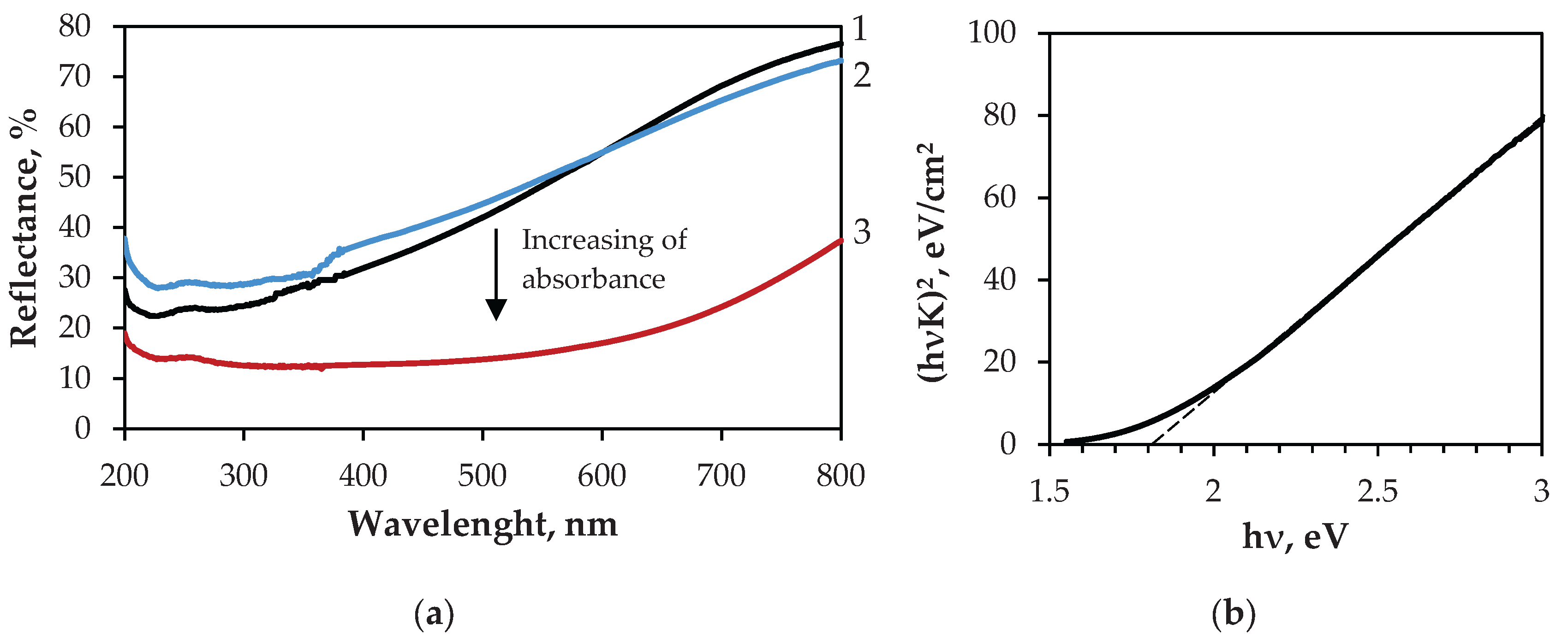
Figure 8.
XRD diffractogram of: 1 – untreated PET/PVC sample; 2 – etched PET/PVC sample; 3 – PET/PVC/Bi-S composite. Peaks are labelled as follows: ● – PET (JCPDS: 50-2275); ○ – PVC (JCPDS: 64-1628); ∆ – rhombohedral CaCO₃ (JCPDS: 05-0586); ▼ – tetragonal TiO₂ (JCPDS: 04-006-1890); □ – orthorhombic Bi₂S₃ (JCPDS: 17-320); ■ – monoclinic S (JCPDS: 76-183).
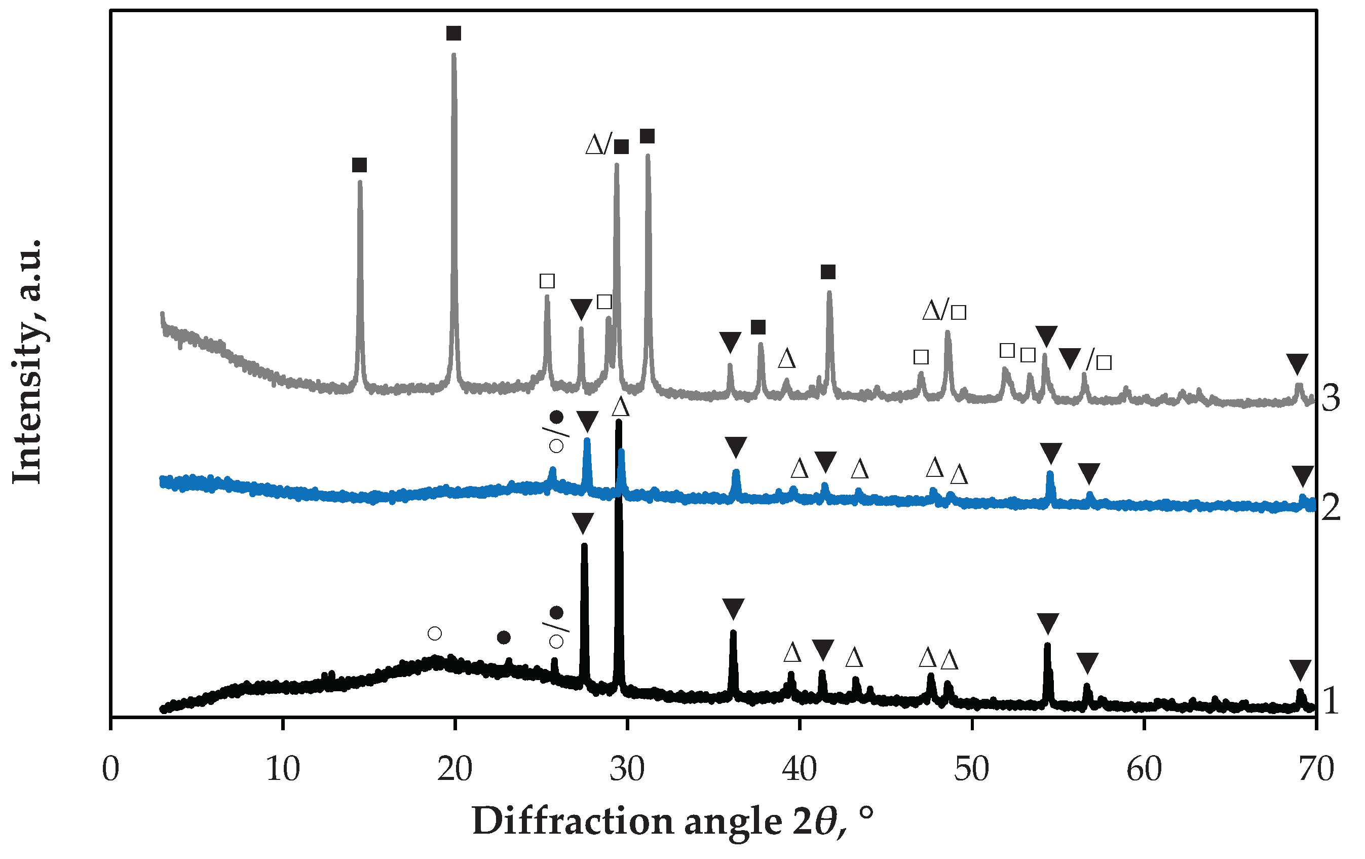
Figure 9.
SEM images of PET/PVC/Bi-S composite: (a) – 300x magnified; (b) – 40000x magnified.
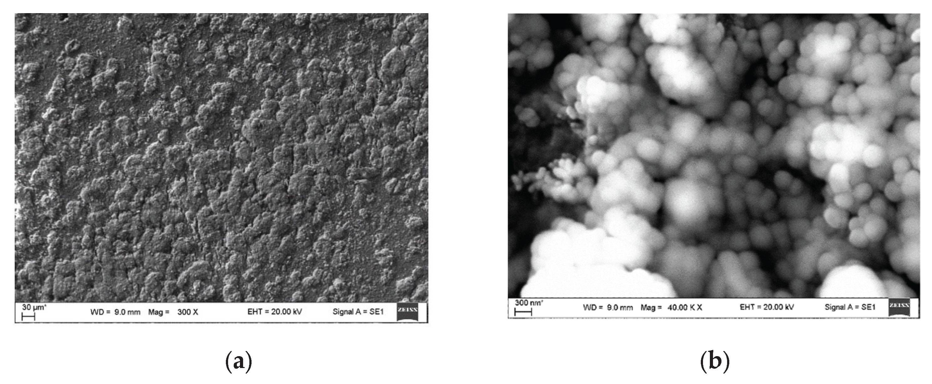
Figure 10.
EDX elemental maps of Bi (yellow) and sulphur (blue) (10000x magnified) of PET/PVC/Bi-S surface: (a) – spatial distribution of elements; (b) – elemental concentration distribution; (c) – representative EDX spectra. The normalised atomic percentages of Bi and S in the films are shown in the corresponding inset.
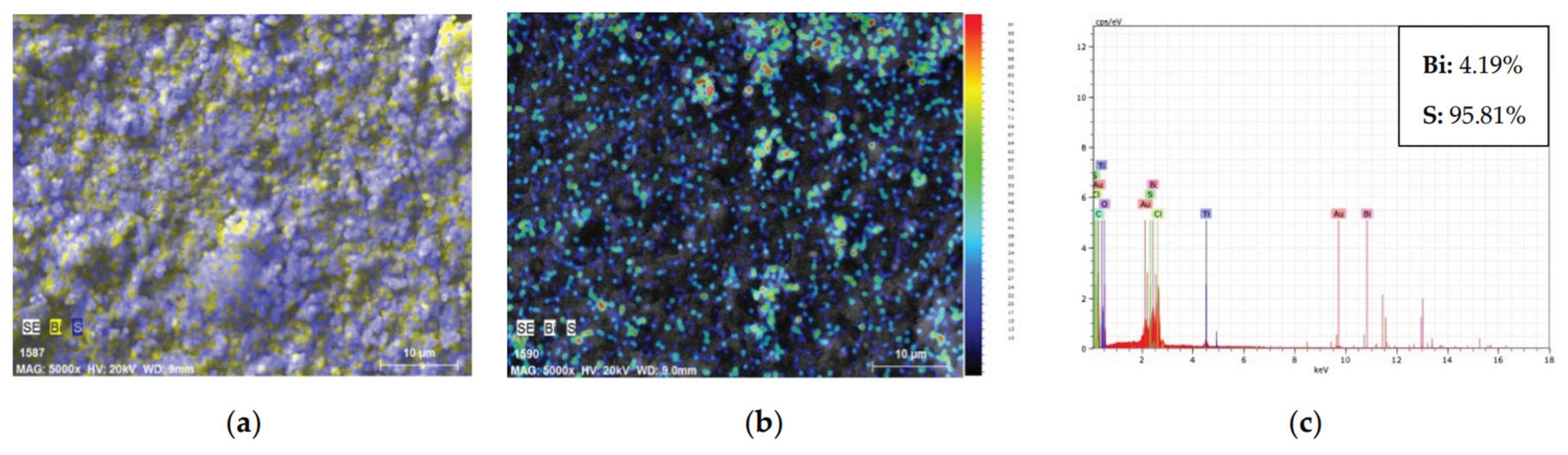
Figure 11.
(a) Optical reflectance spectra as a function of the wavelength in the range of 200–800 nm for: 1 – untreated PET/PVC; 2 – etched PET/PVC; 3 – PET/PVS/Bi-S composite. Photograph of the PET/PVC/Bi-S sample shown in the inset; (b) Eg determination by Kubelka – Munk method.
Figure 11.
(a) Optical reflectance spectra as a function of the wavelength in the range of 200–800 nm for: 1 – untreated PET/PVC; 2 – etched PET/PVC; 3 – PET/PVS/Bi-S composite. Photograph of the PET/PVC/Bi-S sample shown in the inset; (b) Eg determination by Kubelka – Munk method.
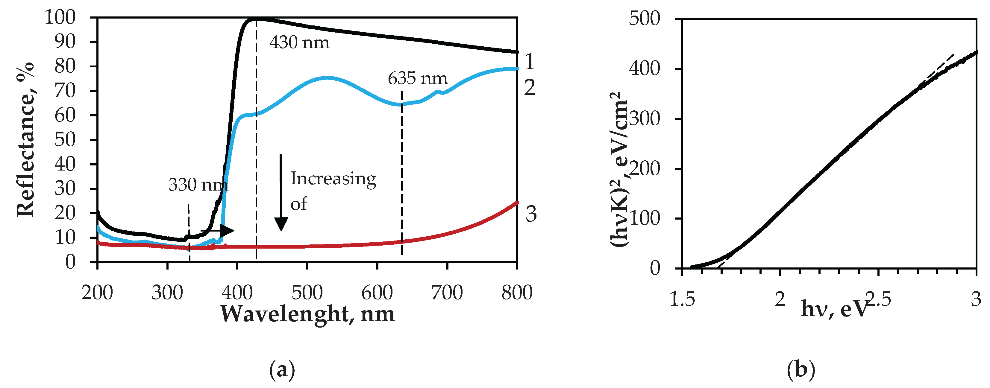
Figure 12.
XRD diffractogram of samples: 1 – C/PES/S; 2 – C/PES/S/Bi-S. The peaks are labelled as follows: Δ – cotton (JCPDS: 03-0226); ▼ – orthorhombic Bi₂S₃ (JCPDS: 17-320).
Figure 12.
XRD diffractogram of samples: 1 – C/PES/S; 2 – C/PES/S/Bi-S. The peaks are labelled as follows: Δ – cotton (JCPDS: 03-0226); ▼ – orthorhombic Bi₂S₃ (JCPDS: 17-320).
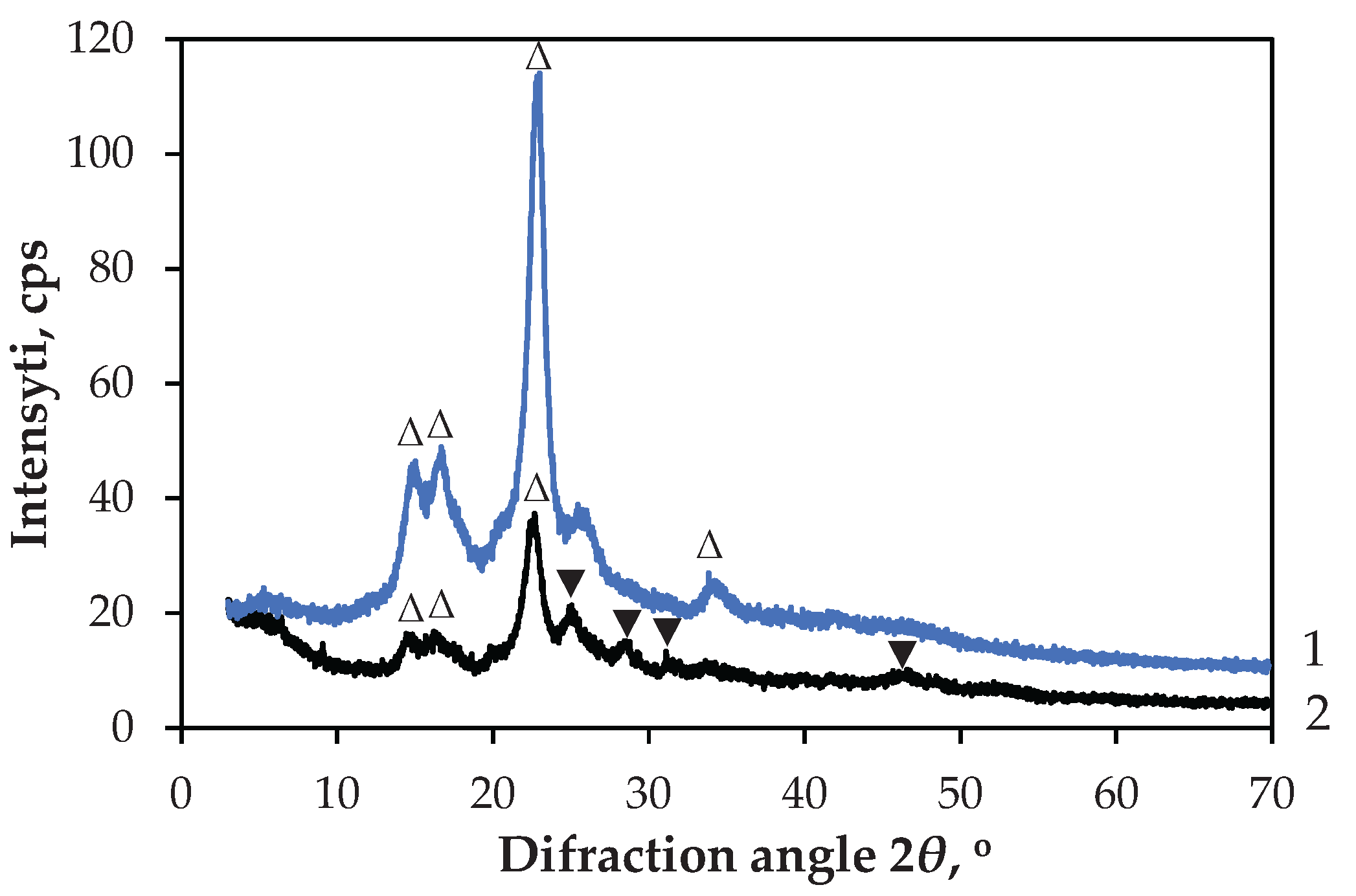
Figure 13.
SEM images of C/PES/S/Bi-S composite: (a) – 300x magnified; (b) – 40000x magnified.
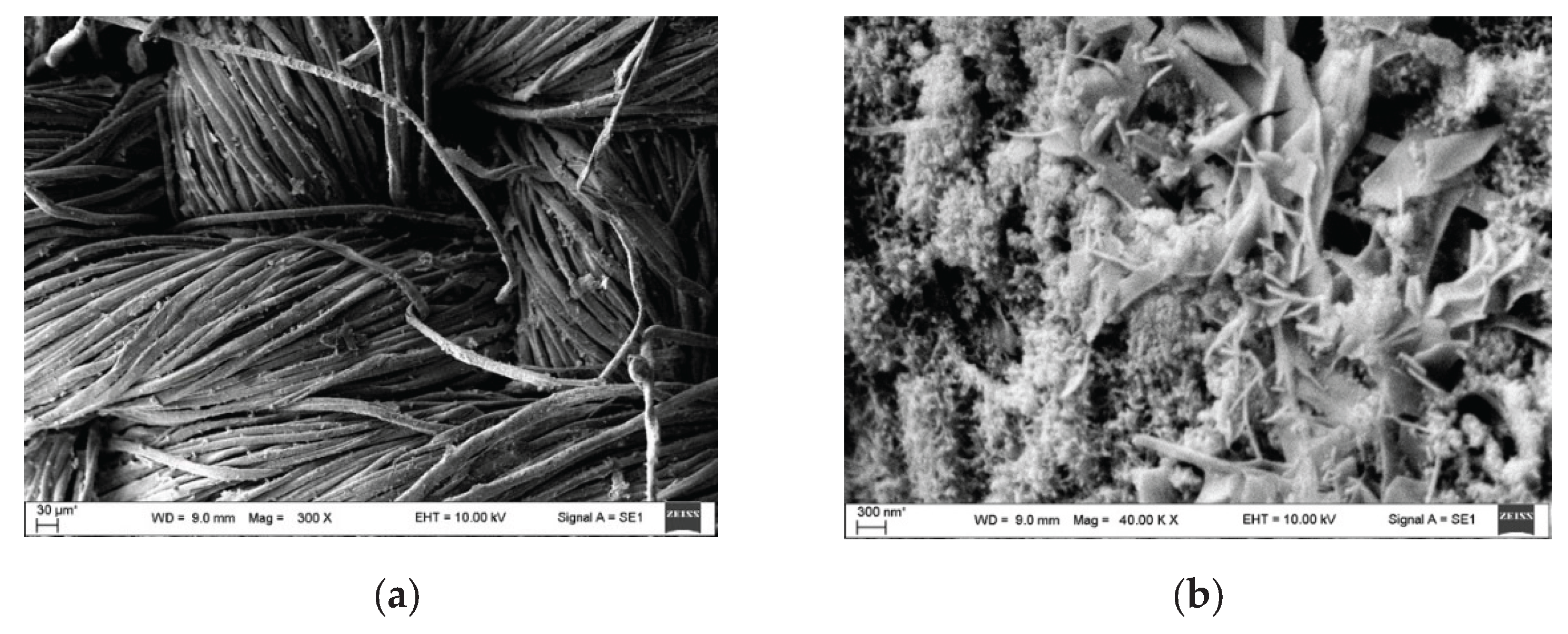
Figure 14.
EDX elemental maps of Bi (yellow) and sulphur (blue) (10000x magnified) of C/PES/S/Bi-S surface: (a) – spatial distribution of elements; (b) – elemental concentration distribution; (c) – representative EDX spectra. The normalised atomic percentages of Bi and S in the films are shown in the corresponding inset.
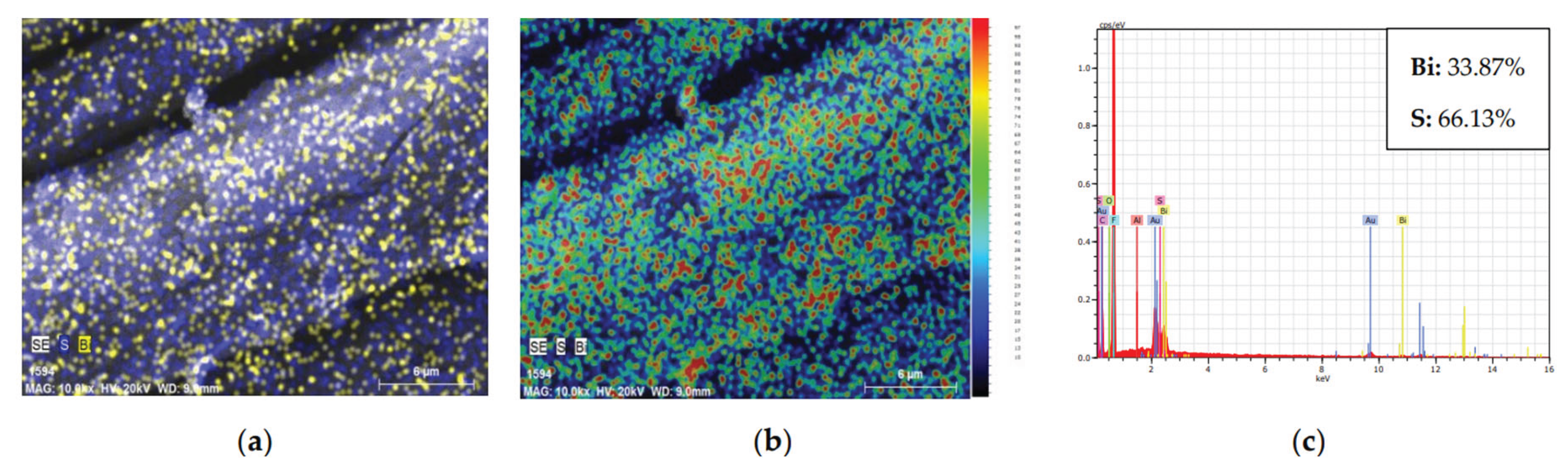
Figure 15.
(a) Optical reflectance spectra as a function of the wavelength in the range of 200–800 nm for samples: 1 – C/PES/S; 2 – C/PES/S/Bi-S. Photograph of the C/PES/S/Bi-S sample shown in the inset; (b) Eg determination for C/PES/S/Bi-S by Kubelka – Munk method.
Figure 15.
(a) Optical reflectance spectra as a function of the wavelength in the range of 200–800 nm for samples: 1 – C/PES/S; 2 – C/PES/S/Bi-S. Photograph of the C/PES/S/Bi-S sample shown in the inset; (b) Eg determination for C/PES/S/Bi-S by Kubelka – Munk method.
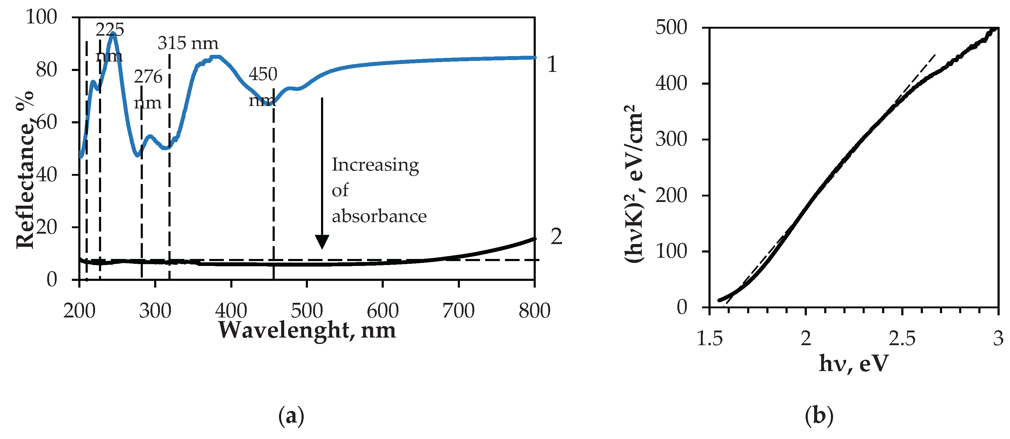
Figure 16.
XRD diffractogram of samples: 1 – PA/Cu; 2 – PA/Cu/Bi-S. The peaks are labelled as follows: Δ – PA6 (JCPDS: 022-0700); ▼ – Cu (JCPDS: 003-1018).
Figure 16.
XRD diffractogram of samples: 1 – PA/Cu; 2 – PA/Cu/Bi-S. The peaks are labelled as follows: Δ – PA6 (JCPDS: 022-0700); ▼ – Cu (JCPDS: 003-1018).
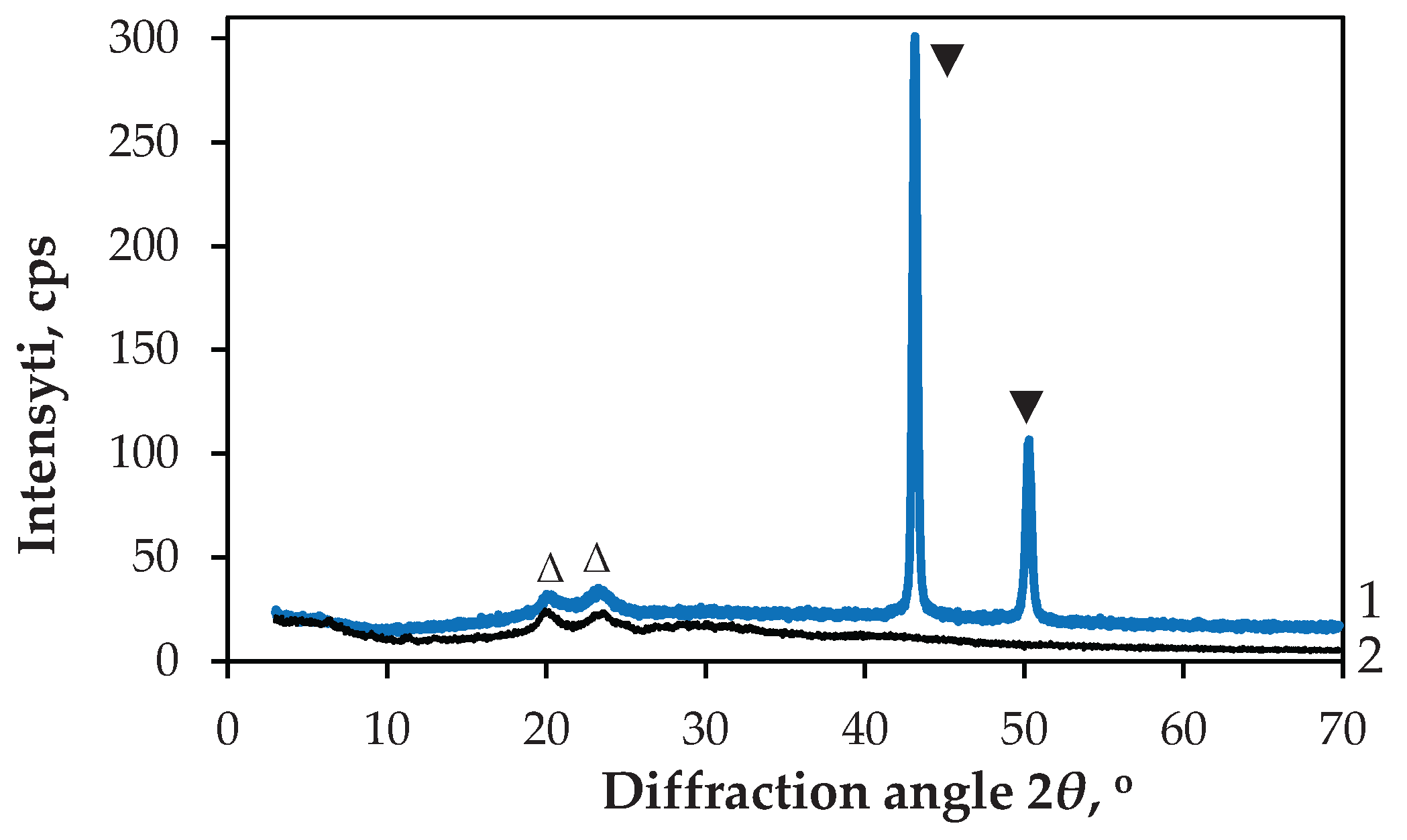
Figure 17.
SEM images of PA/Cu/Bi-S composite: (a) – 300x magnified; (b) – 40000x magnified.
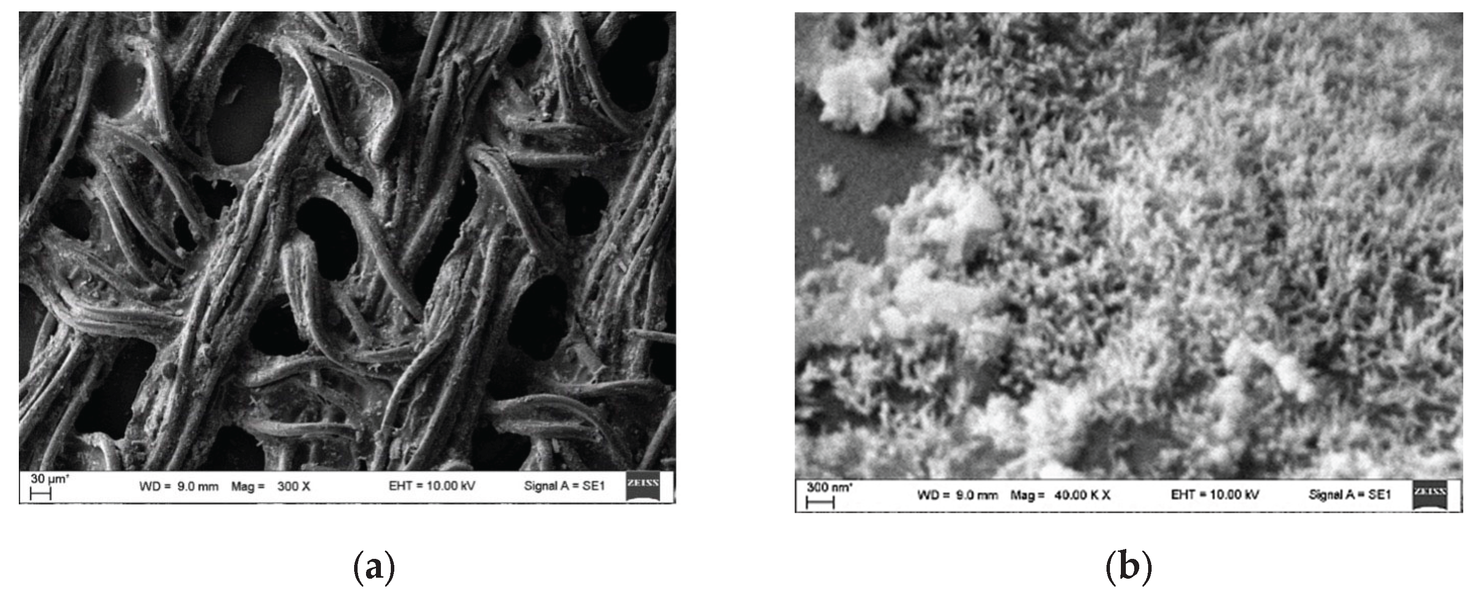
Figure 18.
EDX elemental maps of Bi (yellow) and sulphur (blue) (10000x magnified) of PA/Cu/Bi-S surface: (a) – spatial distribution of elements; (b) – elemental concentration distribution; (c) – representative EDX spectra. The normalised atomic percentages of Bi and S in the films are shown in the corresponding inset.
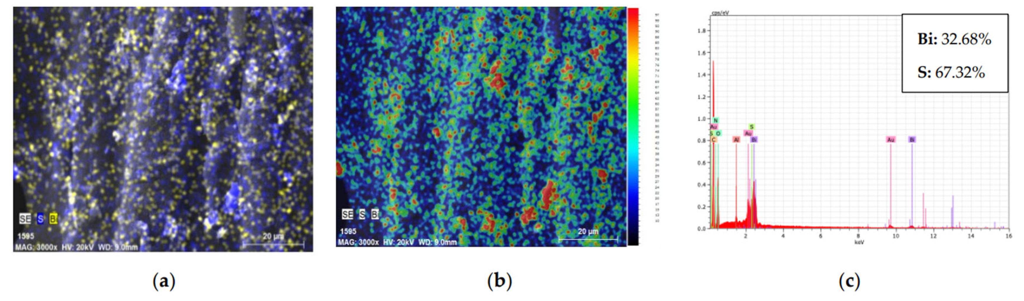
Figure 19.
(a) Optical reflectance spectra as a function of the wavelength in the range of 200–800 nm for samples: 1 – PA/Cu; 2 – PA/Cu/Bi-S. (b) Eg determination for PA/Cu/Bi-S by Kubelka–Munk method.
Figure 19.
(a) Optical reflectance spectra as a function of the wavelength in the range of 200–800 nm for samples: 1 – PA/Cu; 2 – PA/Cu/Bi-S. (b) Eg determination for PA/Cu/Bi-S by Kubelka–Munk method.
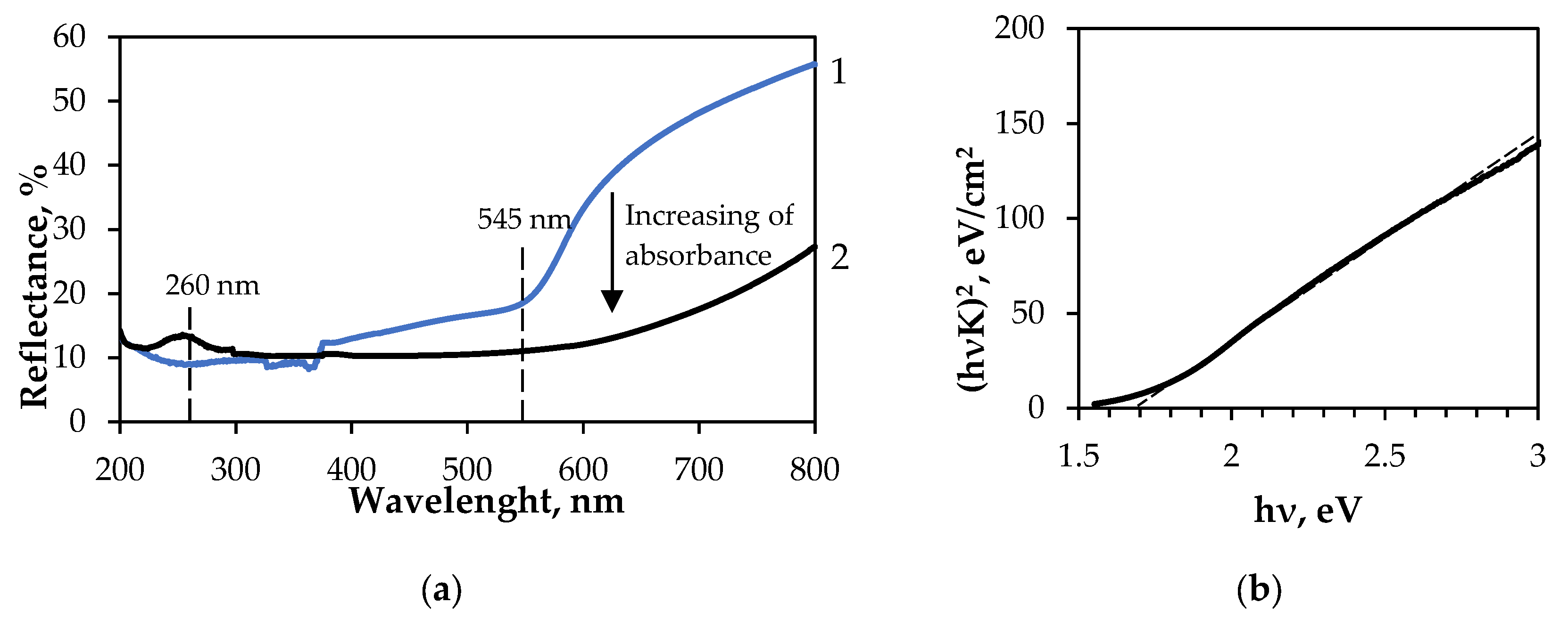
Figure 20.
XRD diffractogram of samples: 1 – PA/Ag; 2 – PA/Ag/Bi-S. The peaks are labelled as follows: Δ – PA6 (JCPDS: 12-923); ▼ – Ag (JCPDS: 04-0783).
Figure 20.
XRD diffractogram of samples: 1 – PA/Ag; 2 – PA/Ag/Bi-S. The peaks are labelled as follows: Δ – PA6 (JCPDS: 12-923); ▼ – Ag (JCPDS: 04-0783).
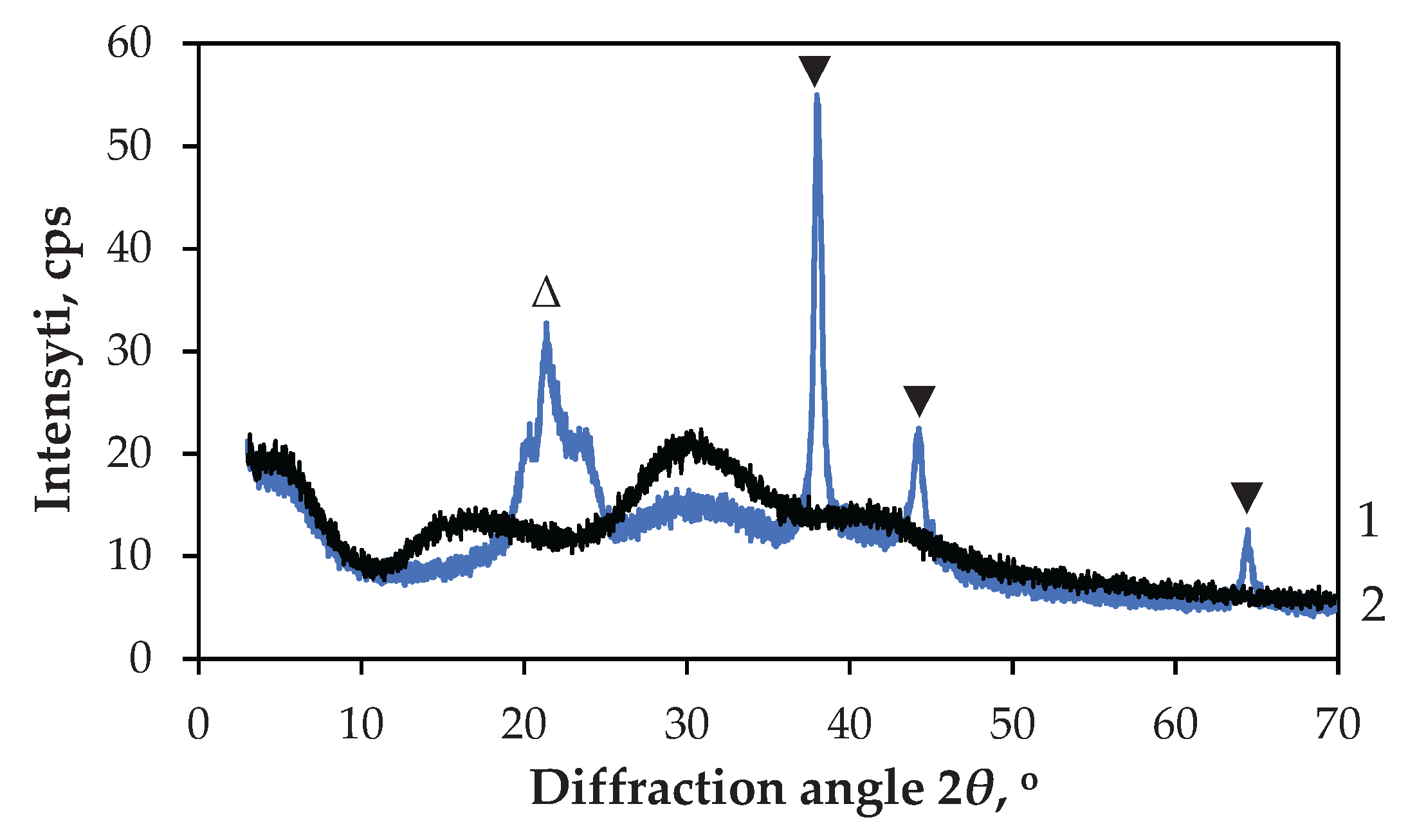
Figure 21.
SEM images of PA/Ag/Bi-S composite: (a) – 300x magnified; (b) – 40000x magnified.
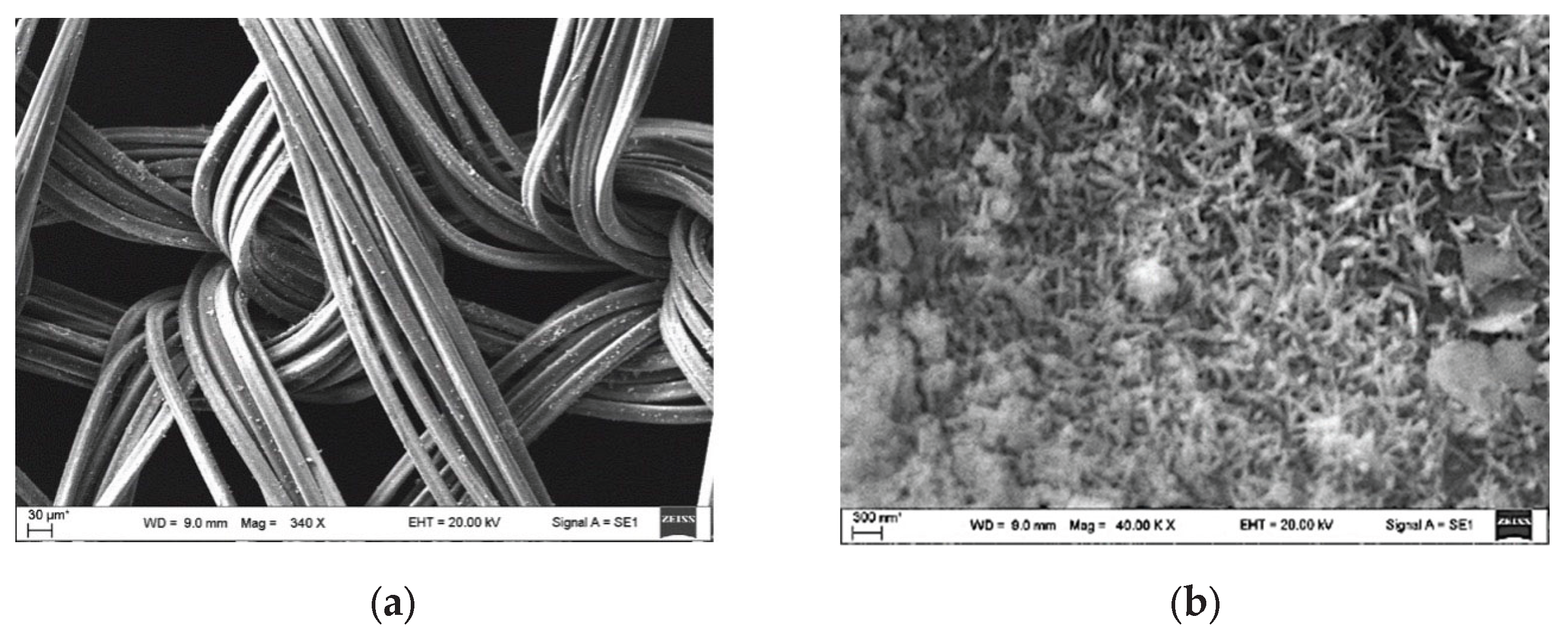
Figure 22.
EDX elemental maps of Bi (yellow) and sulphur (blue) (10000x magnified) of PA/Ag/Bi-S surface: (a) – spatial distribution of elements; (b) – elemental concentration distribution; (c) – representative EDX spectra. The normalised atomic percentages of Bi and S in the films are shown in the corresponding inset.
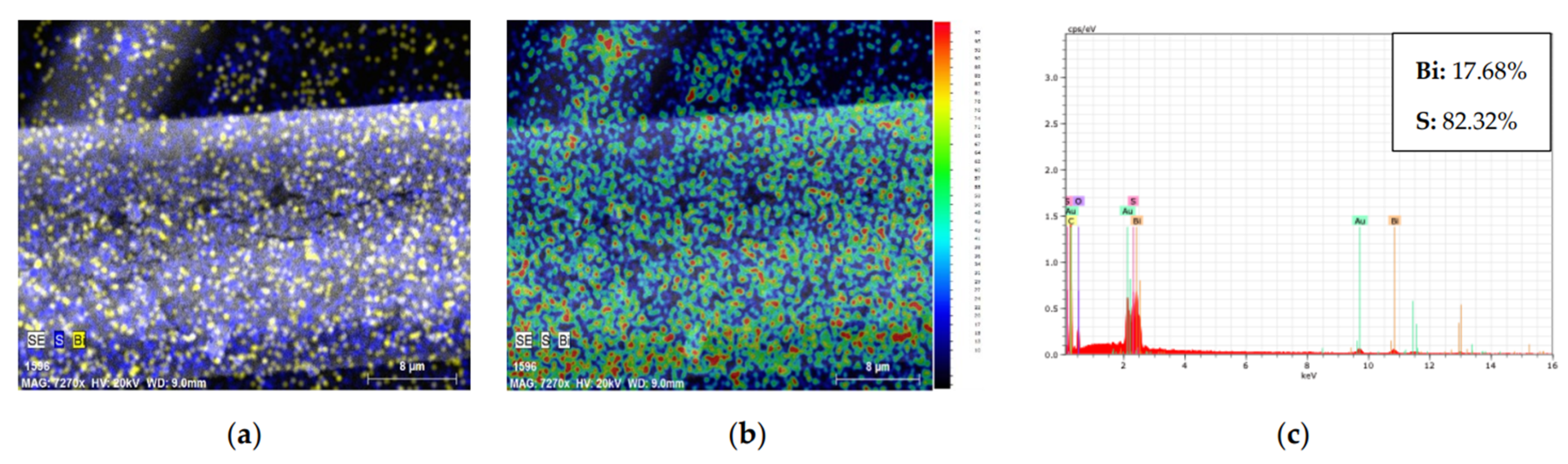
Figure 23.
(a) Optical reflectance spectra as a function of the wavelength in the range of 200–800 nm for samples: 1 – PA/Ag; 2 – PA/Ag/Bi-S. (b) Eg determination for PA/Ag/Bi-S by Kubelka – Munk method.
Figure 23.
(a) Optical reflectance spectra as a function of the wavelength in the range of 200–800 nm for samples: 1 – PA/Ag; 2 – PA/Ag/Bi-S. (b) Eg determination for PA/Ag/Bi-S by Kubelka – Munk method.
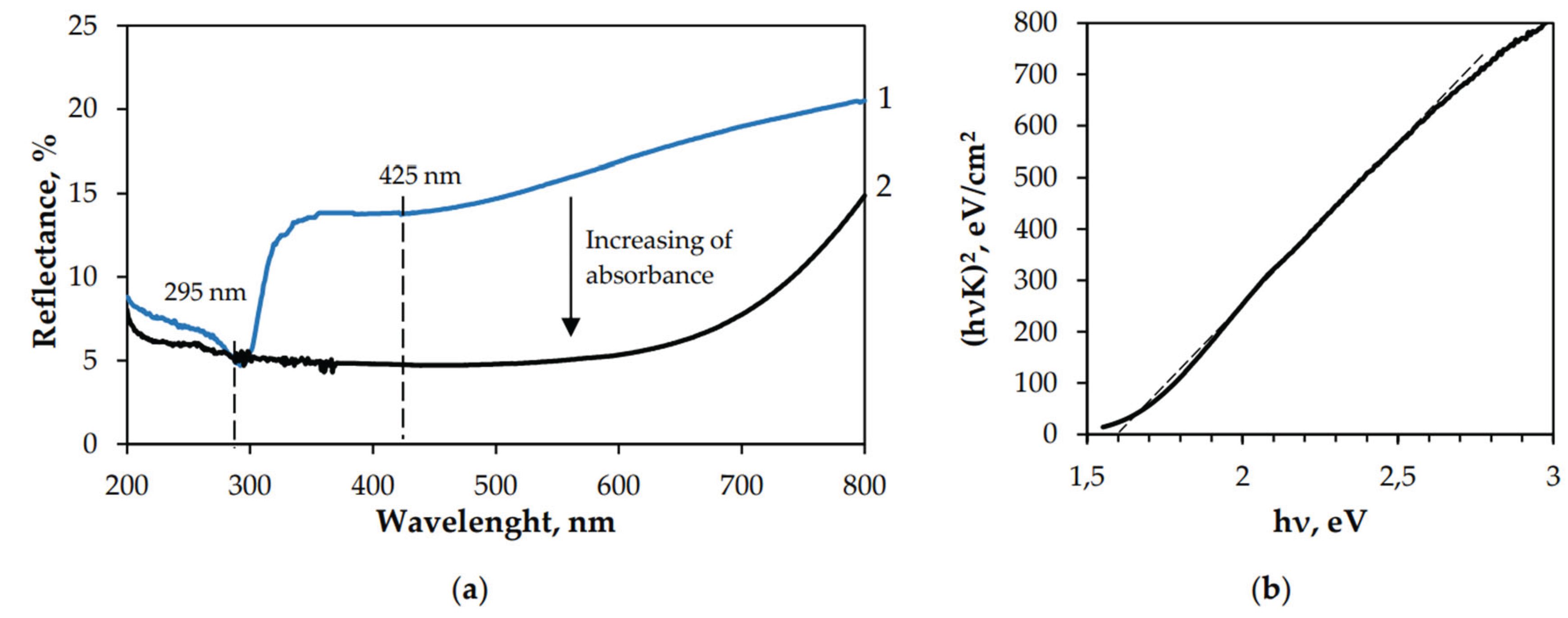

Table 1.
Photographs of samples and technical data of textiles provided by manufacturers.
| Textile | GF/PTFE | PET/PVC | C/PES/S | PA/Cu | PA/Ag |
|---|---|---|---|---|---|
| Photographs |  |
 |
 |
 |
 |
| Composition | PTFE-coated fiberglass | PET yarn, coating PVC, filler 1 | 75% cotton (C), 24% polyester (PES), 1% spandex (S) 2 | 100% nylon (PA), metallisation copper (Cu) | 100% nylon (PA), metallisation silver (Ag) |
| Thickness, mm | 0,58 | 0,56 | 0,35 | 0,05 | 0,10 |
| Basis weight, g/m2 | 1100 | 850 | 290 | 52 | 34 |
| Heat resistance, ℃ | 260 | 70 | 80 | 30 | 30 |
| Cold resistance, ℃ | -73 | -30 | -30 | -30 | -30 |
1 The filler pigment is not specified, but XRD analysis showed that the dominant inorganic fillers are CaCO3 and TiO2 (XRD results are presented in Subsubsection 3.2.2.). 2 The spandex fibre that's most used has at least 85% polyurethane and 15% other materials, like nylon or polyester, in it.
Table 2.
Parameters of thermo-oxidative acid treatment of GF/PTFE and PET/PVC samples.
| Solution composition and concentration, M |
Sample | Etching conditions | |
|---|---|---|---|
| Temperature, °C | Duration, h | ||
| H2SO4, 7.2 H3PO4, 6.6 CrO3, 0.36 |
GF/PTFE | 2 | |
| PET/PVC | 2 | ||
Disclaimer/Publisher’s Note: The statements, opinions and data contained in all publications are solely those of the individual author(s) and contributor(s) and not of MDPI and/or the editor(s). MDPI and/or the editor(s) disclaim responsibility for any injury to people or property resulting from any ideas, methods, instructions or products referred to in the content. |
© 2025 by the authors. Licensee MDPI, Basel, Switzerland. This article is an open access article distributed under the terms and conditions of the Creative Commons Attribution (CC BY) license (https://creativecommons.org/licenses/by/4.0/).
Copyright: This open access article is published under a Creative Commons CC BY 4.0 license, which permit the free download, distribution, and reuse, provided that the author and preprint are cited in any reuse.


