Submitted:
12 August 2025
Posted:
13 August 2025
You are already at the latest version
Abstract
This paper presents an open and fully Chisel-based hardware acceleration framework tailored for high-performance FPGA platforms, with a specific focus on AMD/Xilinx Alveo UltraScale+ cards. While the high-level synthesis (HLS) flow offered by Xilinx enables rapid deployment and is well-suited for many applications, it can be overly abstract for low-level control scenarios such as ASIC prototyping. The alternative RTL Kernel flow offers finer control but often suffers from the limitations of legacy hardware description languages and the overhead of vendor-specific tooling. To address these limitations, we propose a fully open-source workflow based on Chisel, a modern hardware construction language embedded in Scala. Chisel combines the flexibility of object-oriented programming with the ability to generate synthesizable RTL, enabling scalable, reusable, and modular designs. Our framework demonstrates how Chisel can be used to implement advanced hardware features including AXI4/AXI4-Lite interfacing, multi-clock domain designs, asynchronous communication primitives, and enhanced simulation capabilities such as custom VCD trace generation. The use of the Vivado RTL flow bypasses the constraints imposed by the Xilinx golden image and XRT stack, allowing direct programming and fine-grained control over the FPGA fabric. Lightweight host communication is achieved via the XDMA IP and Linux device files, enabling platform-agnostic integration using standard programming languages such as C++ and Python. As a proof of concept, we implement a high-throughput matrix-vector multiplication engine for floating-point data in a self-alignment format (SAF), fully utilizing the resources of a multi-SLR Alveo U200 card. Benchmark results show efficient pipelined operation and full cross-SLR scalability, validating the viability of the proposed framework for custom acceleration pipelines.
Keywords:
Chisel
; high-end FPGAs
; Alveo
; self-alignment technique (SAT)
1. Introduction
Field-Programmable Gate Arrays (FPGAs) are increasingly central to modern high-performance computing, offering low-latency, highly parallel, and energy-efficient architectures for workloads in signal processing, cryptography, machine learning, and scientific computing [1,2]. Among these, the AMD/Xilinx Alveo UltraScale+ series stands out for its rich logic, memory, and DSP resources, high-speed PCIe and QSFP interfaces, and the ability to span multiple Super Logic Regions (SLRs), enabling large-scale pipelined architectures [3]. However, exploiting this potential remains challenging due to architectural segmentation and the complexity of associated design flows, particularly when working across SLR boundaries where long interconnect delays and limited routing resources introduce stringent timing and placement constraints [4].
To improve developer productivity, AMD/Xilinx provides two primary development flows. The High-Level Synthesis (HLS) flow allows designers to implement hardware from high-level specifications in C/C++, greatly reducing development time and lowering the barrier to entry. HLS has proven successful in a wide range of applications and offers considerable productivity gains [5]. However, it tends to obscure low-level timing and resource control, which can be detrimental in contexts such as ASIC prototyping, fine-grained performance optimization, or latency-sensitive control logic [6].
As an alternative, the RTL Kernel flow exposes low-level control through Verilog or VHDL, enabling tighter integration with custom hardware modules and access to the Xilinx Runtime (XRT) for host interaction [7]. While this flow supports more precise control, it introduces several drawbacks. These include rigid packaging requirements, reliance on proprietary protocols, and challenges in spreading design logic across multiple SLRs due to tool constraints [8]. Furthermore, workflows built around Vitis and XRT are tightly coupled to the AMD/Xilinx software stack, which can lead to portability issues and non-negligible host-side overheads, such as memory alignment constraints and bandwidth limitations [9].
To address these limitations, we propose a fully open-source hardware development framework based on Chisel (Constructing Hardware in a Scala Embedded Language) [10], a hardware construction language that enables designers to describe parameterizable and modular hardware using object-oriented programming constructs. Chisel generates synthesizable Verilog or SystemVerilog code compatible with standard FPGA design tools such as Vivado, making it particularly suitable for both FPGA acceleration and ASIC prototyping workflows [11,12].
Our framework integrates cleanly with the Vivado RTL flow. Host communication is achieved through the open-source XDMA interface [13], enabling lightweight interaction with the FPGA fabric via platform-agnostic file I/O using C++ or Python. This setup provides the benefits of direct RTL control while avoiding the overhead of vendor-managed partial reconfiguration flows.
The main contributions of this paper are as follows:
- The framework natively supports AXI4 and AXI4-Lite interfaces [16], multi-clock domain design, and asynchronous communication primitives – all developed in pure Chisel including the top-level module, promoting portability and maintainability.
- We demonstrate a proof-of-concept accelerator: a high-performance, pipelined floating-point matrix-vector multiplication engine based on the Self-Alignment Format (SAF) [17]. The design is mapped across all three Super Logic Regions (SLRs) of an AMD/Xilinx Alveo U200 FPGA [18], validating both performance and cross-SLR scalability.
- We provide the first full Chisel implementation of the SAF arithmetic format [17], demonstrating the framework’s capability to express non-trivial numerical operators in a modular and reusable form.
- All source code, including the SAF accelerator, Chisel framework modules, and simulation/testbench infrastructure, is released as open source and made freely available via a GitHub repository [19] to encourage reproducibility and community adoption.
The remainder of this paper is organized as follows: Section 2 presents background material. Section 3 details the proposed design methodology and Chisel-based development flow. Section 4 provides a comprehensive evaluation of the framework, including performance and resource utilization metrics. Section 5 discusses architectural implications, limitations, and future extensions. Finally, Section 6 concludes the paper and outlines potential avenues for future research.
2. Background
2.1. Hardware Platform
2.1.1. The UltraScale+ Architecture
AMD / XIlinx UltraScale is a series of high-performance, server acceleration- and ASIC prototyping-oriented FPGA chips [3]. The UltraScale+ XCU200 FPGA used to implement the proof-of-concept for this paper embeds over 1M LUT and 2M flip-flops, 960 UltraRAM blocks, 6840 DSP slices, along with several clock trees, MMCM / PLL resources, and DDR4 RAM, PCIe, QSFP connection capabilities. This enables the development of real-world, performance-oriented accelerator cards [20], multi-FPGA architectures, high-throughput, multi-clock designs. Moreover, ASIC-like clocking capabilities enable using UltraScale+-based devices for ASIC prototyping [21].
2.1.2. Super Logic Regions and Inherent Design Constraints
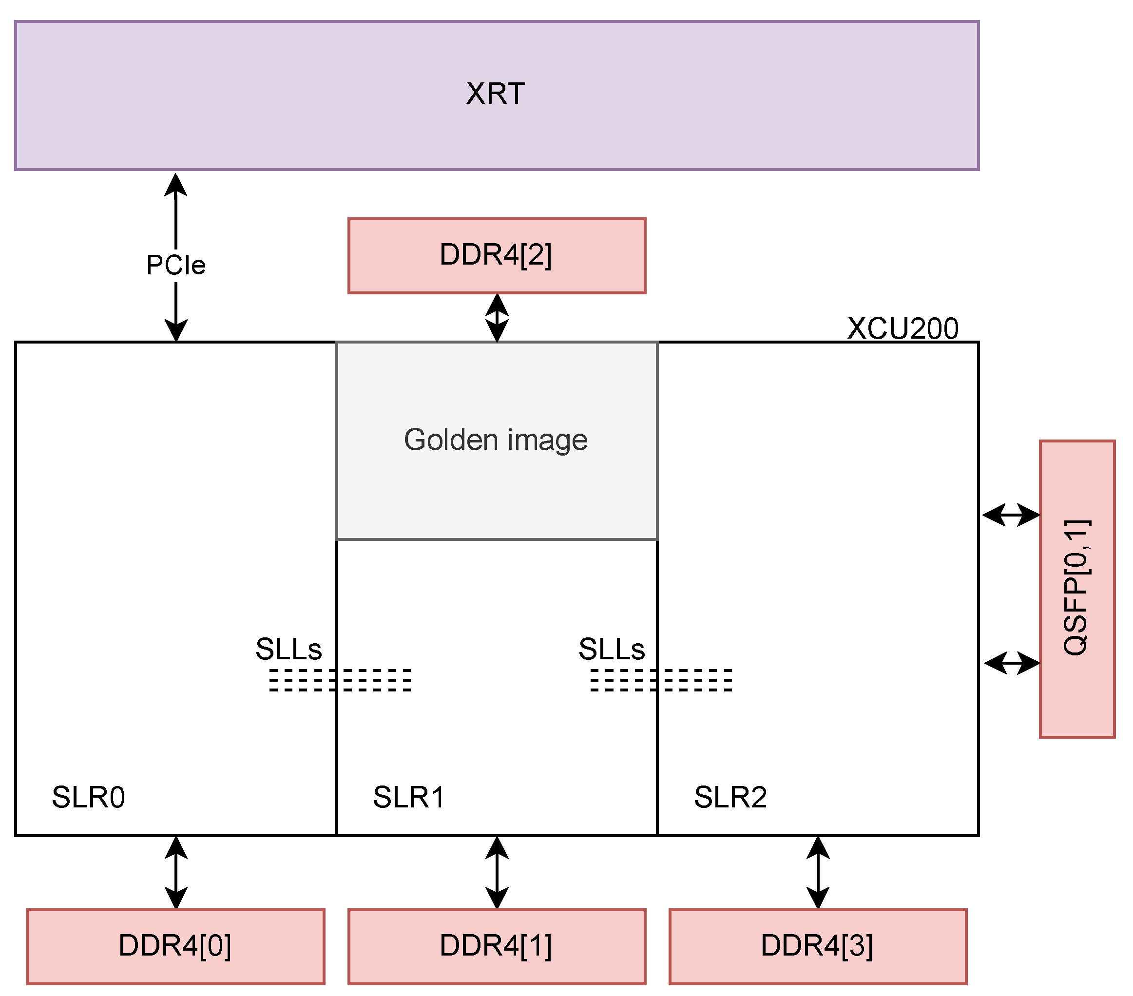
The creation of such large FPGA architectures are enabled by Xilinx’s Stacked Silicon Interconnect technology, which allows to create large-scale "virtual FPGAs" by interconnecting several standard FPGAs, while still satisfying ASIC prototyping-grade performance and timings [22]. However, this modular design implies new constraints on the designer, by dividing the programmable logic resources into several Super Logic Regions (SLR). The XCU200 has 3 such regions (see Figure 1); other models may have 2 or 4 SLRs.
While these multi-SLR architecture enable implementing larger-scale designs, it also entails harder constraints on the designer. In fact, connectivity is limited between SLRs, and the Super Long Lines (SLL) crossing the SLR boundaries enforce pipelining constraints to ensure timing closure [23]. Section 3 details how these constraints were overcome by designing a modular, block-organized design. which allows the placer to easily cross SLR boundaries without compromising timings.
2.1.3. The Alveo Platforms
AMD / Xilinx Alveo cards [20] are server acceleration-oriented, high-throughput FPGA boards based on the UltraScale+ architecture. They enable real-world integration by exposing PCIe Gen3x16 and QSFP interfaces, populating the internal chip’s clock trees with several clocks pre-tuned for various applications (such as QSFP and PCIe clocking, PLL / MMCM division). Alveo cards also embed up to 64GB DDR4 RAM chips, optional active cooling and JTAG or PCIe programming capabilities [24].
The default AMD / Xilinx design flow for Alveo boards hinges on dynamic reconfiguration capabilities of a golden image – a static IP pre-programmed in one of the FPGA’s SLRs (see Figure 1). In combination with the Xilinx RunTime (XRT) library, the Alveo golden image allows dynamic reconfiguration of the FPGA by sending the bitstream through the PCIe interface, using an executable on the host. Moreover, the golden image embeds AXI Master DMA, PCIe peer-to-peer, direct usage of the host memory (bypassing the DMA) through PCIe, dynamic reconfiguration at runtime capabilities [25]. Among other usages, this allows the card to be used as a memory master controller, and is easily used in combination with PYNQ [26], an open-source Python layer for interacting with FPGA that abstracts the hardware and XRT calls into user-friendly Python classes.
While these capabilities of the golden image allow for faster and easier accelerator development, the golden image / XRT framework and the associated RTL kernel design flow also entails some non-negligible limitations.
- The golden image takes up a fixed amount of resources: according to UG1120 [25] (in section "U200 Gen3x16 XDMA base_2 Platform"), it consumes little less than one third of the available LUT and FF in SLR1, and roughly half of the available RAM and URAM blocks in SLR1. This results in roughly 18% of the LUT and FF, and 15% of the RAM tiles (URAM and BRAM). The replacement used in this design uses approximately 11000 LUT (0.9%), 14000 FF (9.5%) and 31 RAM blocks (1.4%) – see 2.1.5.
- The XRT library is packaged only for some yum and APT-based Linux distributions and officially supports some versions of Ubuntu, RHEL and CentOS [28], which needlessly constrains the host platform OS.
- The framework enforces pre-defined host-card control and data transfer protocols [29]. While these are particularly integrated with HLS flows, they prevent the designer from using custom IP cores for AXI communication, and impose Xilinx’s IP cores, which may not reach the AXI4 protocol’s full throughput [30].
- In the RTL kernel design flow, the Vitis linker is able to place each kernel in a user-defined SLR [31], but this entails that cross-SLR boudary communication is always implemented with AXI4 protocols, which can have non-necessary repercussions on design complexity and restrain ASIC prototyping applications.
2.1.4. The Vivado RTL Flow
To address the limitations presented in the previous section, we chose to completely drop the Vitis RTL kernel design flow in favor of the standard Vivado synthesis flow. To achieve this, the golden image is replaced by the Xilinx Direct Memory Access (XDMA) Intellectual Property (IP). It is instantiated as a black-box module in the design, allowing for RTL-only conception in any RTL-capable language, such as Chisel, SystemVerilog or VHDL.
The absence of a golden-image prevents dynamic reconfiguration with Xilinx binaries, but the board can be programmed through JTAG from the Vivado Hardware Manager, as would be any external Xilinx FPGA-based board. The most notable advantage of dropping the golden image is resource utilization, as precised in the next section.
In this design flow, the whole synthesis, implementation and bitstream generation process is managed entirely by Vivado, allowing for a simpler software usage. Moreover, the design constraints can be fully declared using Xilinx’s XDC format and the scripting capabilities of Vivado can be leveraged to optimize synthesis and implementation processes.
The only hard drawback of this workflow is the need for PCIe rescanning after each board flash, which can lead to bricking the host OS. The safe method for reflashing used in the development of this paper consists in hot-rebooting the host, such that the hosts’s hardware can properly detect the PCIe bus before booting Linux, while keeping the FPGA’s dynamic memories programmed with the design. However, this could be prevented by programming the FPGA’s static configuration memory at each reflash. Moreover, in a production environment, the FPGA’s static memory would be programmed once and cold reboots wouldn’t impact its configuration.
2.1.5. XDMA and Host-Card Communication
As stated in the previous section, the XDMA IP is used to manage host-card communication in place of the Xilinx golden image.
The XDMA IP has two operating modes [32]. This design uses the "DMA" mode, which converts PCIe transactions into master AXI4 and AXI4-Lite transactions. It exposes one (optional) AXI4-Lite interface, M_AXI_LITE, and one master AXI4 interface, M_AXI, with up to 4 channels for both reading and writing (see Figure 2b). This configuration allows the user design to be used as a subordinate to the XDMA, which is in turn controlled through PCIe by a driver on the host system. The kernel software stack is managed by Xilinx’s open-source DMA driver [33], which creates a character device (under /dev) that can be interacted with using standard file Input-Output (IO). Thus, any file-IO capable language can be used to develop user applications that interact with the design.
A high-level overview of the design blocks is presented in Figure 2a. The user logic kernel must be an AXI4-compliant slave to interact with the XDMA, preventing the user from designing a PCIe subsystem from scratch and allowing to focus on the core logic, with the minimal overhead of AXI4 compliance. The XDMA IP handles the whole PCIe clocking and transaction logic, and even generates a clock and a reset for the AXI buses.
In order to truly use the PCIe’s DMA capabilities and to initiate transactions from the PL, the XDMA IP can be used in "AXI Bridge" mode, which exposes an additional memory-mapped AXI4 slave interface on which transactions are converted to PCIe memory-mapped transactions. Unfortunately, the designer would have to code a dedicated driver to obtain physical memory addresses to send to the PL. However, while this operating mode could be useful for designs requiring high-throughput data-flows, the present proof-of-concept doesn’t need such functionality.
2.2. Chisel
2.2.1. Introducing Chisel
Chisel (which stands for "Constructing Hardware In a Scala-Embedded Language") is a hardware construction language that enables designers to describe parameterizable and modular hardware using object-oriented programming constructs [34]. Chisel generates synthesizable Verilog or SystemVerilog code compatible with standard FPGA design tools such as Vivado, making it particularly suitable for both FPGA development and ASIC prototyping workflows [9,12]. By leveraging Chisel’s abstraction capabilities, designers can reduce boilerplate, promote code reuse, and express complex hardware architectures using modern metaprogramming techniques [11].
Although based on a high-level language, Chisel remains a RTL-level Hardware Description Language (HDL). exploits the flexibility of the Scala programming language by providing a set of primitives for hardware description, and by allowing deep and fine parametrization. For instance, Chisel promotes the use of Bundles – which are similar to VHDL record, although more flexible – for defining IO interfaces, which can then easily be reused to define registers or flipped equivalent interfaces.
The Chisel code produced is compiled into FIRRTL, an intermediate representation of the circuit, in the form of an abstract syntax tree (AST). The Chisel code is reduced in several steps before reaching its most simplified stage. Finally, a corresponding Verilog or SystemVerilog file is produced [35,36].
Figure 3 presents the design flow of a hardware module using the Chisel language. The design is first described in a Scala file, using Scala native libraries and the Chisel library (which implements the hardware concepts discussed below). The Scala compiler then produces a class to be used by a Java virtual machine specific to Chisel. This virtual machine produces an FIR file, which is an intermediate RTL representation of the described design. Finally, the FIRRTL representation is used to generate Verilog or SystemVerilog code.
Chisel aims to express "flexible and scalable circuit construction" by using the concept of circuit generators. Generators aim to raise the level of abstraction in order to allow for aggressive parametrization and constraining, while still generating synthesizable and optimized RTL code [40]. To the designer, this construction makes it very easy to generate several versions of the same design from one single code-base, by varying certain parameters.
One main particularity of Chisel is that the default clock and reset of synchronous modules are implicit [38], which means the designer doesn’t need to declare them in the default module generator, Module. Registers are instantiated with the Reg construct, which automatically creates a register clocked with the current scope’s (often implicit) clock. Multi-clocked designs can however be described by manually specifying explicit clocks in certain scopes [41]. Among several Scala building tools, this project uses Scala Build Tool (SBT) [42] to build Chisel projects and run Chisel.
2.2.2. Chisel Testing Capabilities
Chisel module simulation is handled by the ChiselSim [38] library, which interfaces Scala test-bench classes with the svsim [39] backend. svsim aims to be a backend-agnostic simulation infrastructure, which simulates Chisel-generated Verilog with ChiselSim-generated test-benches. The default lower-level simulation backend is Verilator [43].
Simulation was ported to svsim after Chisel version 6.0.0, until which chiseltest [44] was used. In this process, the Value Change Dump (VCD) generation feature offered by chiseltest was lost. Fortunately, since Verilator is capable of generating VCD traces, simple Scala hacks exist that allow to recover this important feature. The proof-of-concept design presented here uses a fork of edwardcwang’s MIT-Licensed repository [15,45], visible in Figure 3.
The ChiselSim API offers methods to "peek", "poke" and "expect" values on design ports, which allow verifying the module’s behavior based on assertions, without actual need for VCD traces. Thus, a module specification can be written in Scala, and automated tests can be run and verificated.
In a Chisel test-bench, timings are completely abstracted to the user, and all value changes occur on the falling edge of the module’s clock. While this really eases test-bench design, it also constrains the design; ChiselSim natively only support single-clock, synchronous designs. The methodology in this paper details how these limitations were worked around to enable real-life design testing with Chisel.
2.3. Floating-Point Formats
Floating-point arithmetic is a fundamental aspect of numerical computation, enabling efficient representation and manipulation of a wide range of real numbers. The IEEE-754 standard is a globally recognized and extensively utilized framework for representing floating-point numbers [46]. However, performing arithmetic operations on IEEE-754 floats in hardware is really expensive, especially in FPGA. Thus, many hardware floating-point arithmetic methods internally use a custom floating-point format, allowing for efficient processing [47].
To expose the flexibility of Chisel, the proof-of-concept design presented in this paper integrates a compile-time condition to choose between two floating-point arithmetic implementations: a custom Self-Aligned Format (SAF) [17] and Berkeley’s hardfloat [48].
2.3.1. Self-Alignment Technique
The first floating-point arithmetic method is based on the so-called self-alignment technique (SAT) [49,50,51], with a custom self-aligned format (SAF) [17]. This method allows creating single-cycle accumulators and multipliers with limited or non-existent precision loss [17]. However, in the current implementation, simplicity was preferred over precision for the proof-of-concept architecture, thus the SAF implementation used doesn’t showcase the best capabilities of the method. To implement the SAF computations, work previously made in HLS [52] was ported from C++ HLS to RTL hardware in Chisel.
SAF is defined with two parameters: L, the number of low-order bits from the exponent that are passed to the mantissa, and w, the width of the extended mantissa . The SAF reduced exponent is bits wide. A number f represented in SAF is stored as (reduced exponent, extended mantissa). The reduced exponent bias b is given by the base bias of the floating point format (127 in our case), plus the width of the base float mantissa, (23 with IEEE-754 binary32 format). Hence, . The value of f can be retrievd by:
In the present proof-of-concept, SAF parameters are chosen with values . Additional parameters which can ensure conservation of the float precision such as and g [17] are not implemented, thus ignored.
The SAFMAC module implements a pipelined SAF multiply-accumulator (MAC). Inputs are in a custom "expanded" float format, which contains the IEEE-754 8-bit biased exponent, and a signed, expanded mantissa which contains the integer bit. The "expanded" floats are 33 bits wide. The multiplier converts the floats to SAF, and the accumulator stores results in SAF, which are 73 bits wide.
2.3.2. Berkeley’s Hardfloat
As a demonstration of the capabilities of Chisel, a hardware floating-point arithmetic library was developed fully in Chisel by the Berkeley University of California and released under a customized BSD 3-clause open-source license [48]. berkeley-hardfloat [53] uses an internal recoded floating-point format on 33 bits for computations, and offers modules to convert between formats and to perform arithmetic operations. The recoded floating point format is not documented, but from the source code it can be seen that it is the same format as the "expanded" format described in the previous section.
Figure 4 shows the three floating point storing formats used.
3. Implementation Methodology
3.1. Matrix-Vector Multiplication Applicative Core
To showcase the proposed framework for real-life, multi-clock designs in Chisel with Vivado RTL flow, a floating-point matrix-vector multiplication applicative core was developed and integrated in the framework. The core realizes the operation presented in Equation (1), where m and n are integers defining the height and the width of the matrix. The coefficients of the matrix, , are programmable, and the input vector is the input data.
While the core module is not the main focus of this paper, some design decisions have been taken because of the particular, multi-SLR architecture of the target platform. The design consists in a strongly pipelined chain of computing units – named "workers" in the following – that communicate with one another with reduced-width buses. Each worker has its own finite state machine (FSM), enabling it to be dependent only on the input data streams accompanied that minimalist control signals, thus facilitating placement and timing closure on multi-SLR platforms. Moreover, the base component of the design, a hardware floating-point mutliply-accumulator, is pipelined to help reduce critical path lengths.
Equation (1) is mapped such that each worker performs the dot product of one row of the matrix and the input vector. To do so, each worker stores its corresponding row coefficients in an internal memory, and multiply-accumulates the incoming vector into a result register upon receiving input. When the whole input vector has been received, the workers send their result through the pipeline, which is then routed to the outer communication layers by the controller.
3.1.1. Floating-Point Multiply-Accumulators
The core arithmetic is realized by a pipelined multiply-accumulator (MAC), presented in Figure 5.
To help timing closure, the MAC is pipelined between multiplication and accumulation, which isolates the paths traversing the digital signal processors (DSP) between two pipeline registers. The DSP are necessary for multiplication but also introduce a high timing overhead.
To showcase the templating capabilities of Chisel, the MAC are defined with either hardfloat or SAF adders and multipliers. The library used is determined at compile time by a Scala if condition on the design parameter USE_HARDFLOAT, which acts as a conditional templating method for Chisel. This way, the use of SAF or hardfloat can be specified on the command-line when compiling the Chisel project.
3.1.2. Applicative Matrix-Vector Multiplication Pipeline
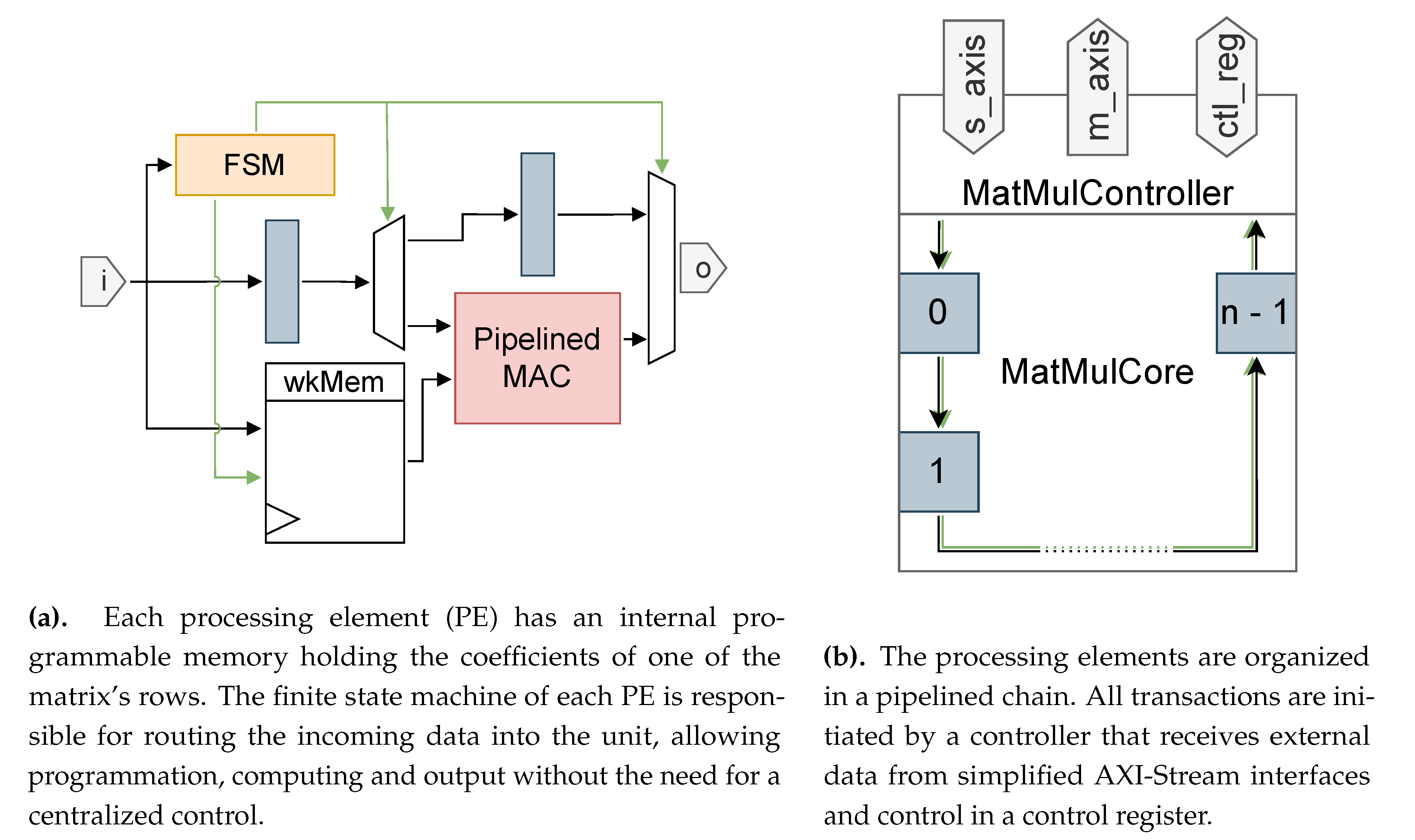
The actual computing is done by the Worker module, which schematics is given in Figure 6a. These processing elements (PE) are connected sequentially to one another and thus form a pipelined chain as shown in Figure 6b, allowing routing on mulit-SLR FPGA. Taking advantage of the object-oriented features of Chisel, the workers’ interfaces are defined as the WorkerInterface bundle, which allows easily connecting the workers together. Moreove, each PE has a wid input that is set to a constant representing the PE’s position in the pipeline, allowing its finite state machine (FSM) to determine the pipeline’s state without having to receive control signals from a centralized controller.
Three control signals are transmitted along each data packet between the PE:
- valid indicates valid data on the bus;
- prog specifies that the data is to be programmed in a PE memory;
- write specifies that the data was generated by a PE and is meant to be output.
Each PE computes the vector-vector multiplication of one of the matrix’s rows and the input vector. It holds the coefficients of its matrix row in an internal (programmable) synchronous-read memory, and uses the pipelined MAC detailed in Section 3.1.1 to compute its output coefficient. When programming, the FSM counts the incoming coefficients and forwards them up to the ones destined to its PE memory. When receiving a valid data without the prog flag set, the PE multiplies it with the corresponding coefficient, accumulates it, increases its memory pointer, and forwards the data to the next PE. Once the m coefficients have been received, each PE receives the values computed by the preceding PEs in the chain with write set, forwards them to the next PE (or the controller), and appends its own computed result to the transaction. The first PE in the chain, with wid 0, generates the write signal itself.
The controller module MatMulController receives and sends data streams on simplified AXI-Stream [54] interfaces, s_axis and m_axis (s_ stands for "slave" and m_ for "master"). When bit 0 of the control register at address 0 is set to 1 through the control register interface ctl_reg, the next data packets input through s_axis are sent to the pipeline with the prog flag set. Once transactions have been received on s_axis, the next m values are sent as the input vector. The controller will wait for the pipeline to output its results before authorizing new inputs on s_axis. The pipeline outputs are then sent to m_axis, which should end in a FIFO.
Figure 6.
Pipelined processing elements compute the matrix-vector product by computing one dot product each by multiplication-accumulation (signals in green are control signals).
Figure 6.
Pipelined processing elements compute the matrix-vector product by computing one dot product each by multiplication-accumulation (signals in green are control signals).
Leveraging Chisel’s templating capabilities, n and m are defined as design parameters, allowing to specify the matrix’s dimensions at System-Verilog emission time, on the SBT command line.
3.2. Multi-Clock Domain Design in Chisel
The XDMA IP outputs a clock and a reset for the design’s AXI buses, namely axi_aclk and axi_aresetn. It also exposes master AXI4 and AXI4-Lite interfaces for communication with the core module (see Figure 2b). Depending on the configuration of the IP, axi_aclk can run at 150 or 250 MHz, which can be limitating. Moreover, it is not a free-running clock, and the XDMA manuals advise not to use it as a system clock [32]. The Alveo U200 offers several general-purpose clocks; however their use requires strong synchronization mechanisms.
3.2.1. Metastability and Synchronization
When designing with multiple clocks, clock domain-crossing mechanisms must be enforced at the domain boundaries to avoid metastability phenomena [55,56,57,58]. Generally speaking, in the base case one bit of data has to move from a register in the source clock domain to another register in the destination domain. When the two domains are asynchronous, the data lines on the input of the destination register can change at any time in the destination’s clock cycle. If switching happens during the setup or hold time of the register – too close in time to the sampling edge of the clock –, it can enter a metastable state: a state in which the output of the register is undetermined. The metastable state can last indefinitely (with a certain probability [56]) until a later valid sampling, or resolve itself. But the duration of the metastable state is possibly longer than the destination domain’s clock cycle. If this register is sampled while it is in a metastable state, there is no way of determining which state will be interpreted by the subsequent logic, since it depends on the thresholds of the transistors used and other random factors, such as precise voltage of the region and imperfections in the silicon wafer. Several logical paths can even interpret different values, leading to unpredictible logic behavior, and eventually system failure [57]. Figure 7d and Figure 7c present some undesirable metastability-induced phenomena that could occur if the circuit in Figure 7a were to be used in a clock domain crossing context.
In order to safely cross boundaries between asynchronous domains, one must make use of synchronization mechanisms. In the most basic case where only one bit of data must traverse the boundary, mean-time-between-failures (MTBF) calculations ensure that a simple two-flip-flop (2FF) synchronizer as shown in Figure 7b suffices in most cases [56,58,59], even if more successive flip-flops can be added. By the time when the data bit reaches the output of the synchronizer, the possible metastability in the first flip-flop is almost certainly expected to have resolved. But when multiple data bits, or even data streams must cross clock boundaries, stronger mechanisms must be established to ensure safe data transmission. The advanced synchronization methods presented in this paper are reimplementations of Cummings and Golson’s work on synchronization and clock domain crossing [58,59,60] in Chisel.
3.2.2. Multi-Cycle Paths
Multi-cycle paths (MCP) are synchronization mechanisms that allow passing more than one bit of data at a time through a clock domain boundary. Their use allow for punctual word exchange between the domains, which for instance is useful for control register data. They are also used in some asynchronous FIFO designs [58], which will be detailed in Section 3.2.3.
The MCP design is based on the request-acknowledgement (req-ack) handshake principle, with req and ack signals synchronized with 2FF synchronizers. The source controller must emit a pulse on the cross_pulse port of the MCP source, while the data to send is on the data port. When a cross-request pulse is received, the MCP source module toggles the clock domain boundary-crossing load channel, which after synchronization generates a pulse on the load_pulse output of the MCP destination module. Since the payload data was loaded before the load synchronizer, possible metastability on the data port of the output has almost certainly had time to resolve by the time the destination controller receives the signal on the load_pulse port of the destination MCP, if data hasn’t changed. To ensure data is not removed from the MCP source before the load pulse is generated on the destination, the load toggle signal is returned through another 2FF synchronizer as an acknowledgement signal to the MCP source. Only on reception of the ack pulse, the source controller can modify the value on the data port of the MCP source [58,59]. This makes the MCP design very flexible: with the req-ack mechanism, it doesn’t need any information about the relationship between the source and destination clocks, and can transmit data to a faster domain as well as to a slower one.
To comply with Cummings’ guidelines [59] and to easy design in Chisel, the MCP module was separated into two distinct modules, MultiCyclePathSrc in the source domain and MultiCyclePathDst in the destination domain, to keep one single clock per module (see Figure 8).
While this circuit is slower and bigger than the simple 2FF synchronizer, it allows passing data with no single-bit variation constraint. This proves useful in asynchronous FIFO designs, by preventing the use of Gray code pointers [61], which can cross clock domain boundaries using only 2FF synchronizers, but at the cost of encoding in the source domain and decoding in the destination. At last, the resource usage of Gray encoders and decoders remains superior to that of an MCP, while timing gains are mitigated [58].
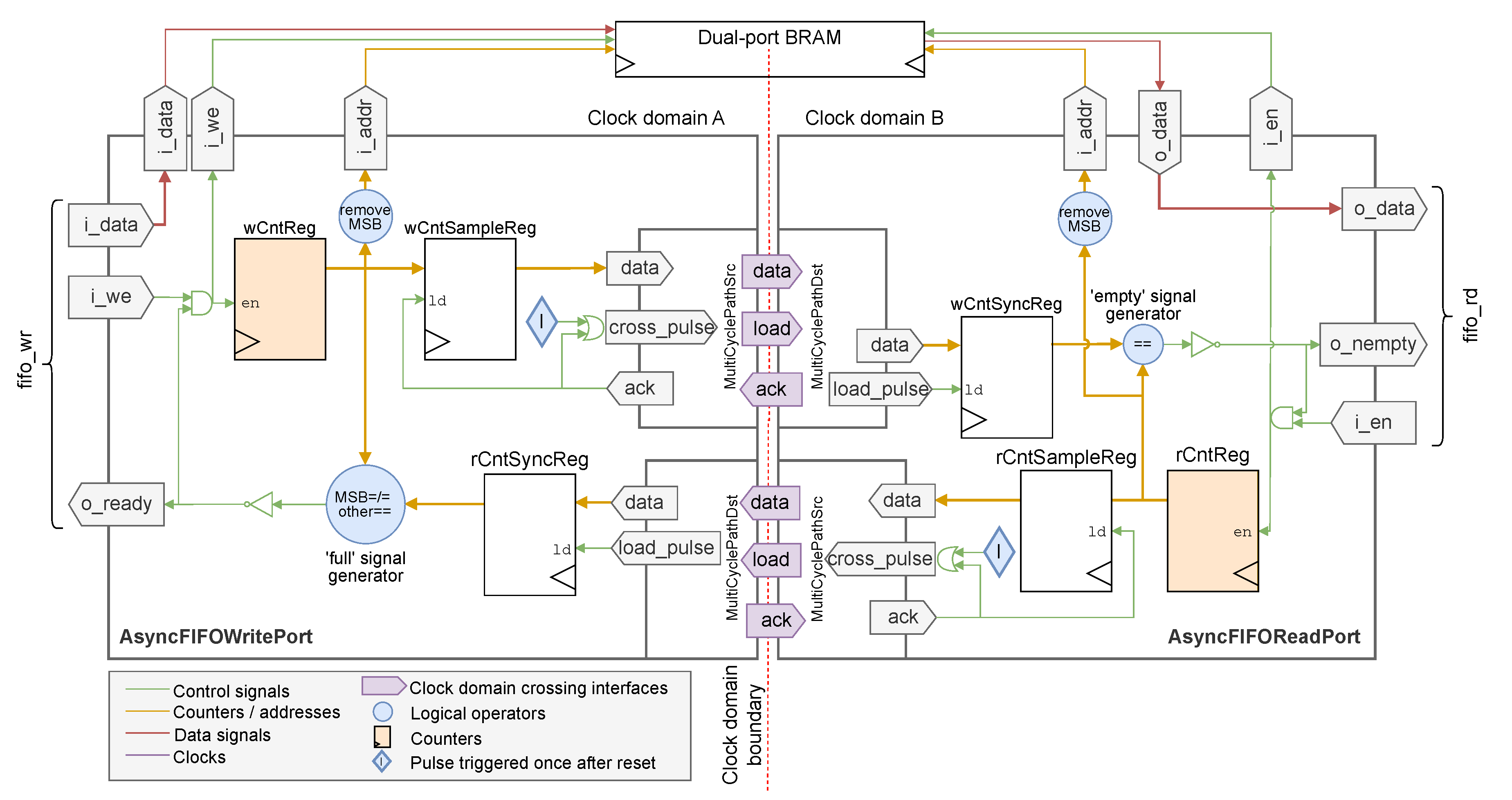
3.2.3. Asynchronous FIFO Queues
When passing streams of data through a clock domain boundary, MCP become too inefficient because of the req-ack mechanism that takes up several clock cycles in both domains to send one single word. In that case, the use of asynchronous FIFO becomes necessary. FIFO are implemented with dual-port RAM blocks: the data emitter writes to the FIFO on one port that is clocked with the source clock, while the receiver reads from the FIFO on its other port which is clocked on the destination clock domain. While this basic mechanism is easy to explain, the major difficulty in FIFO design is pointer synchronization: each clock domain must keep track of the position of the writing or reading head of the other clock domain, to prevent writing to a full FIFO or reading from an empty FIFO. Thus, synchronization mechanisms are needed for pointer crossing.
Still following Cummings’ guidelines [60], the FIFO modules were split on a clock domain basis: one module encloses the FIFO read port, and another module the write port. The actual FIFO memories are instantiated in the top-level module, where each clock domain is present. However, while Cummings recommends Gray code pointers to address FIFO memory, since they only need a simple 2FF [59,60] synchronizer to pass from one domain to the other, the present design uses standard binary counters and synchronizes them through the clock boundary using MCP. This prevents from constraining the FIFO sizes to power of 2, and saves the resources and additional paths needed for multiple conversions between Gray code and standard integer count [58].
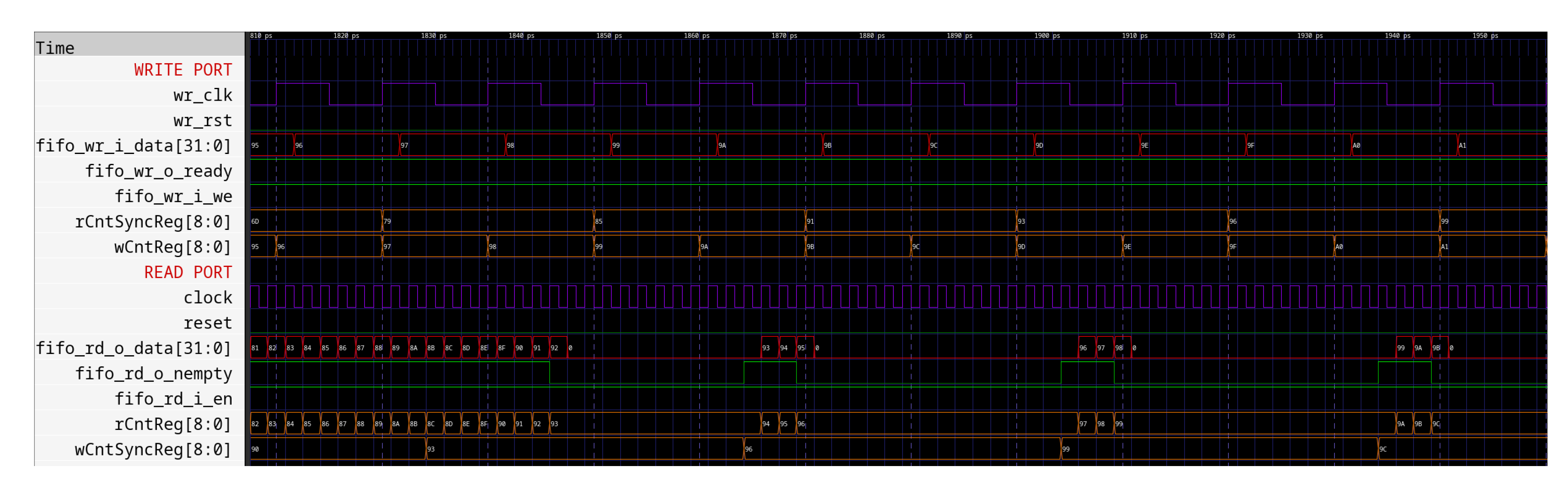
Figure 9 presents an overview of the asynchronous FIFO design used for this proof-of-concept. To generate the full and empty signals, the FIFO uses internal counters that are 1 bit wider than necessary to address the memory. This way, when both counters are equal, the FIFO is empty, whereas when both pointers (meaning, the counters without their most significant bits (MSB)) are equal but the counters’ MSB are different, the write pointer has wrapped over and catched the read pointer: the FIFO is full. This last operation is labeled with MSB=/=other==.
For counter synchronization between the two clock domains, the design uses MCP as described in Section 3.2.2. In each port, the counter is periodically sampled into a register to be sent through a MCP to the other port. After reset, the blocks labeled I trigger this sampling for the first time; once the system is running, sampling is retriggered automatically by the ack signal of the corresponding MCP. The synchronization delays due to the MCP make the full and empty signals "pessimistic" [58]: in the write port, the value of the read counter that is compared with the write counter was sampled several ticks ago, meaning that the read port could have consumed more data by the time when the full signal is generated. This entails that the full signal might be raised while the FIFO memory is not actually full. Similarly, the read port compares an old value of the write counter with its read counter: the actual current value of the write counter could be higher, meaning that more data could be actually available when the empty signal is generated. While this can slow down a very performance-intensive design, this ensures the robustness of this FIFO design [58,60]. An example of this "pessimistic" behavior is shown in the simulation results of Figure 11.
Figure 9.
The asynchronous FIFO design is split into two modules: one for the read port in one clock domain, the other for the write port. The FIFO memory is external to both modules and instantiated in the top-level design, to preserve the "one clock per module" rule.
Figure 9.
The asynchronous FIFO design is split into two modules: one for the read port in one clock domain, the other for the write port. The FIFO memory is external to both modules and instantiated in the top-level design, to preserve the "one clock per module" rule.
3.3. Integration
3.3.1. Communication with the XDMA IP
AXI4-Stream is an easy-to-use, easy-to-implement data bus protocol that allows a controller and a subordinate to communicate while both controlling the debit, thanks to a ready-valid handshake mechanism [54]. Unfortunately, the open-source Linux driver supplied by Xilinx presents some strong limitations when using streaming mode [62,63,64,65,66]. Moreover, the memory mapped AXI4 (AXI-MM) mode allows more flexibility for the underlying IP, for instance by making use of the protocol’s addressing capabilities. For these reasons, the XDMA IP was configured in AXI-MM mode. The AXI4-Lite interface was also added in order to be able to read and write control registers from the host.
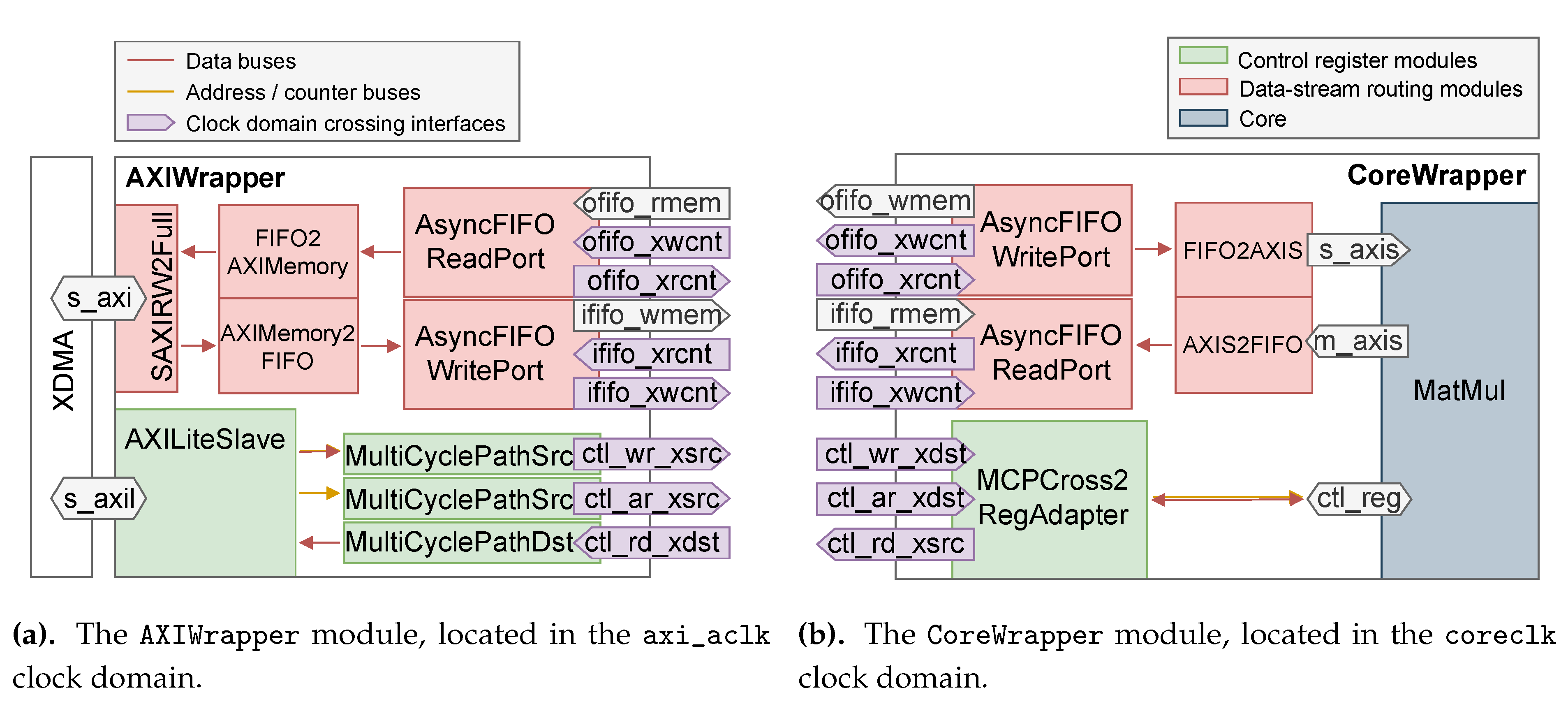
The data entrypoint is SAXIRW2FULL which splits the full AXI4 interface into its read interfaces and its write interfaces. Data input is permitted by the AXI4-compliant AXIMemory2FIFO module, which converts AXI4 write transactions into FIFO write transactions. The other way around, the AXIFIFO2Memory reads into an asynchronous FIFO read port when it receives an AXI4 read request. Finally, the AXILiteSlave module converts AXI4-Lite transactions into simpler register read or write transactions, that are sent through the clock boundary by multi-cycle paths (MCP), which are detailed in Section 3.2.2. For instance, upon receiving a "read address" (AR [67]) request, the given address is sent through the ar MCP. The address is read synchronously in the core’s control register memory, and the corresponding data is sent through the rd MCP back to the AXILiteSlave. The latter the generates an AXI4-Lite read transaction, as requested by the controller (here, the XDMA). The same goes when receiving a write request, except that the wr MCP is one-way, since write operations don’t request feedback from the core.
Similarly, the applicative core is wrapped in the CoreWrapper module shown in Figure 10b, which embeds the necessary asynchronous FIFO ports and multi-cycle path sources and destinations. The FIFO2AXIS module reads the input FIFO as soon as data is available and sends it in simplified AXI-Stream transactions to the core, while the AXIS2FIFO adapter writes the output of the MatMul module into the asynchronous FIFO write port. The MCPCross2RegAdapter receives ar, rd and wr requests from the AXI-Lite slave through the clock region boundary, and reads or writes the core module’s control register accordingly.
To be able to name clocks for clarity, both AXIWrapper and CoreWrapper are defined as Chisel RawModules: Chisel modules without the implicit clock and reset. Hence, their clocks and resets are declared and wired manually, and their submodules are instantiated in withClockAndReset and withClock scopes [68], that allow setting the implicit clock and reset manually within a certain scope of code, as demonstrated in Listing 1.
| Listing 1. withClockAndReset and withClock usage in the CoreWrapper module (wiring is omitted). |
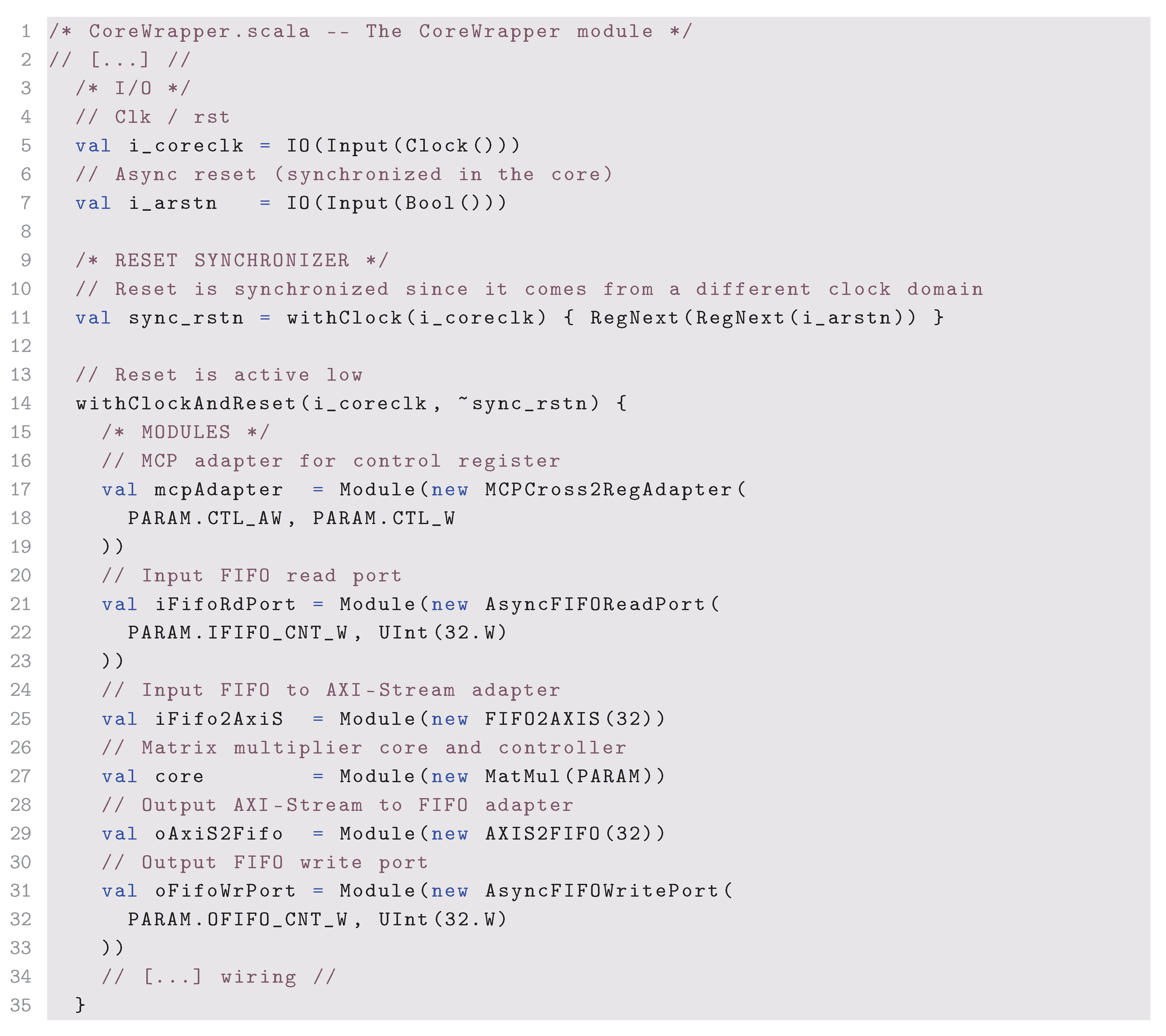 |
Figure 10.
High-level wrappers and their clock domain crossing interfaces, instantiated in the top-level module.
Figure 10.
High-level wrappers and their clock domain crossing interfaces, instantiated in the top-level module.
3.3.2. Top-Level Module
Both wrappers are instantiated in the top-level module, TopLevel. This module is a Chisel RawModule: the clocks are added to the port list and wired to the wrappers manually. Figure 10 is substantially the top-level module, with FIFO memories and clocking logic omitted.
In the Chisel code, BlackBoxes are used to instantiate the XDMA IP and the low-level components necessary to correctly generate the core clock from one of the available differential clocks of the Alveo U200, and to handle resets. The basis for this design was translated from the Vivado-generated XDMA example design, with an added phase-locked loop (PLL) to generate the core clock. The PLL multiplication and division factors (which are parameters of the PLLE4_BASE library module) can be passed directly to the SBT command line, which is parsed into the PARAM object visible in Listings 2 and 3.
| Listing 2. Core clock generation using Chisel BlackBoxes. |
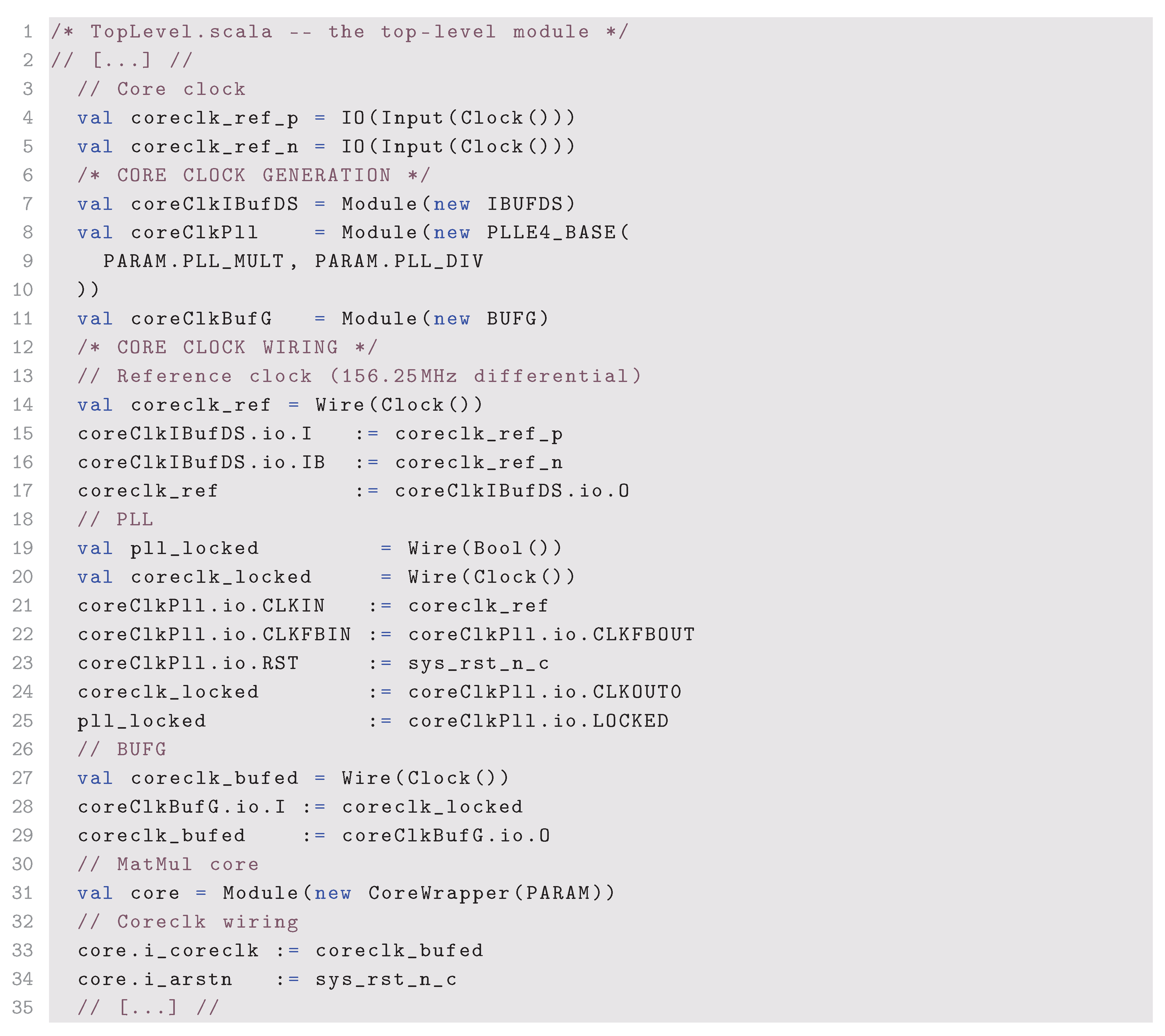 |
Listing 3 demonstrates one of the strengths of Chisel: thanks to its interface bundling features, only seven lines are needed to connect each of the 21 multi-cycle path pins that link AXIWrapper and CoreWrapper across the clock boundary. Similarly, only one line of code is necessary to wire a whole AXI4 interface. This allows faster coding, and cleaner interface declaration and handling by forcing the programmer to wrap the module interfaces into coherent bundles.
| Listing 3. Interface bundles wiring. |
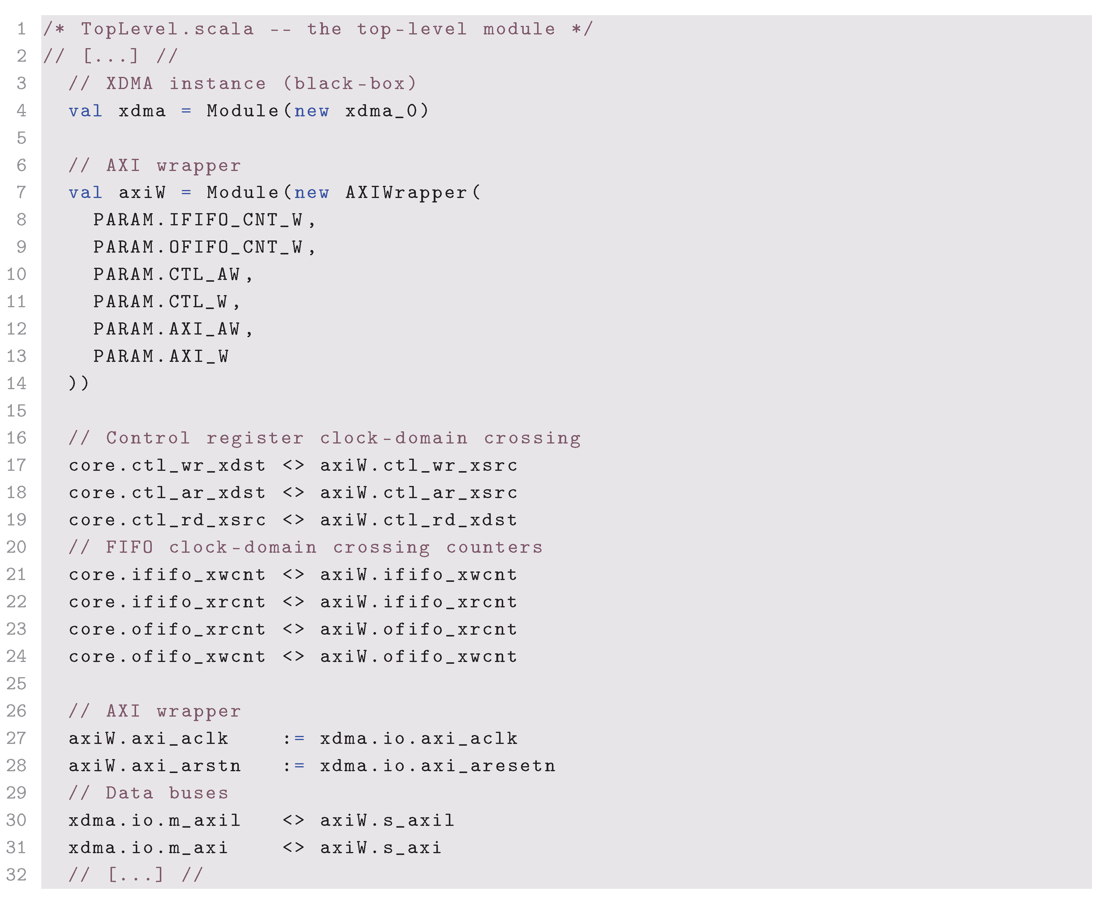 |
3.4. Testing Asynchronous Designs in Chisel
While Chisel offers the possibility to easily define custom clocks and resets overriding the implicit ones, its simulation framework has strong limitations about multi-clocked modules. In fact, trying to simulate a module with several clocks raises an error as Chisel doesn’t officially support this kind of simulation. Using plain Verilog or System-Verilog and Verilator for simulation is a solution to this limitation. However, this loses the object-oriented capabilities of Chisel in the simulation framework, and implies having an heterogeneous codebase that can become hard to maintain. Thus, the present proof-of-concepts presents an alternative that allows simulating multi-clock designs using the integrated Chisel simulation framework.
The proposed testing method takes advantage of the object-oriented capabilities of Scala by creating a FakeClockDivider class, that simulates a divided clock. Its update method takes a Chisel Clock port and toggles after a certain (parametrable) number of calls, simulating a slower clock.
To simulate the multi-clock design, a testing module that encompasses both clock regions is created. For instance, for testing the asynchronous FIFO design, the test module contains both read and write ports of the FIFO, as well as the FIFO memory. This module defines a Chisel Clock input for the slower clock, while the faster clock is mapped to the implicit Chisel clock.
Finally, the Scala test-bench defines a step function that takes the slow clock as an argument and calls both FakeClockDivider.update on it and the unit under test (UUT) clock step method. Listings 4 and 5 show an example based on the FIFO design.
| Listing 4. The FakeClockDivider class. |
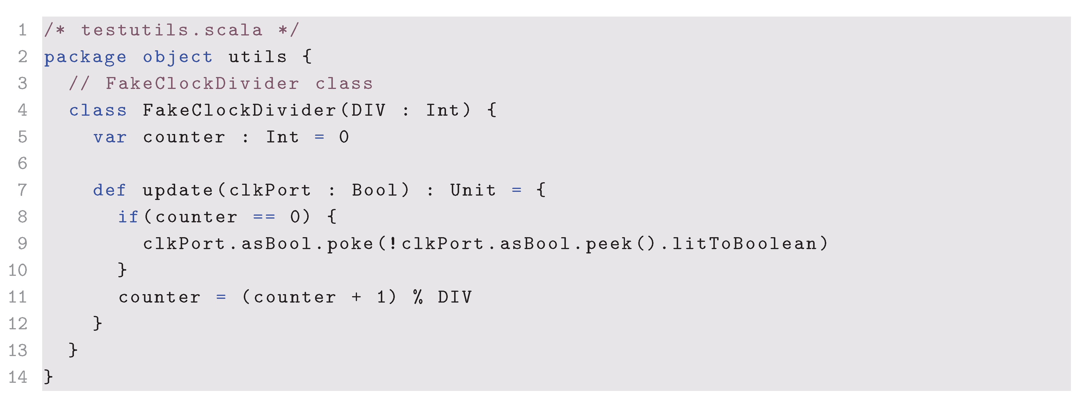 |
| Listing 5. Asynchronous test module and test-bench. |
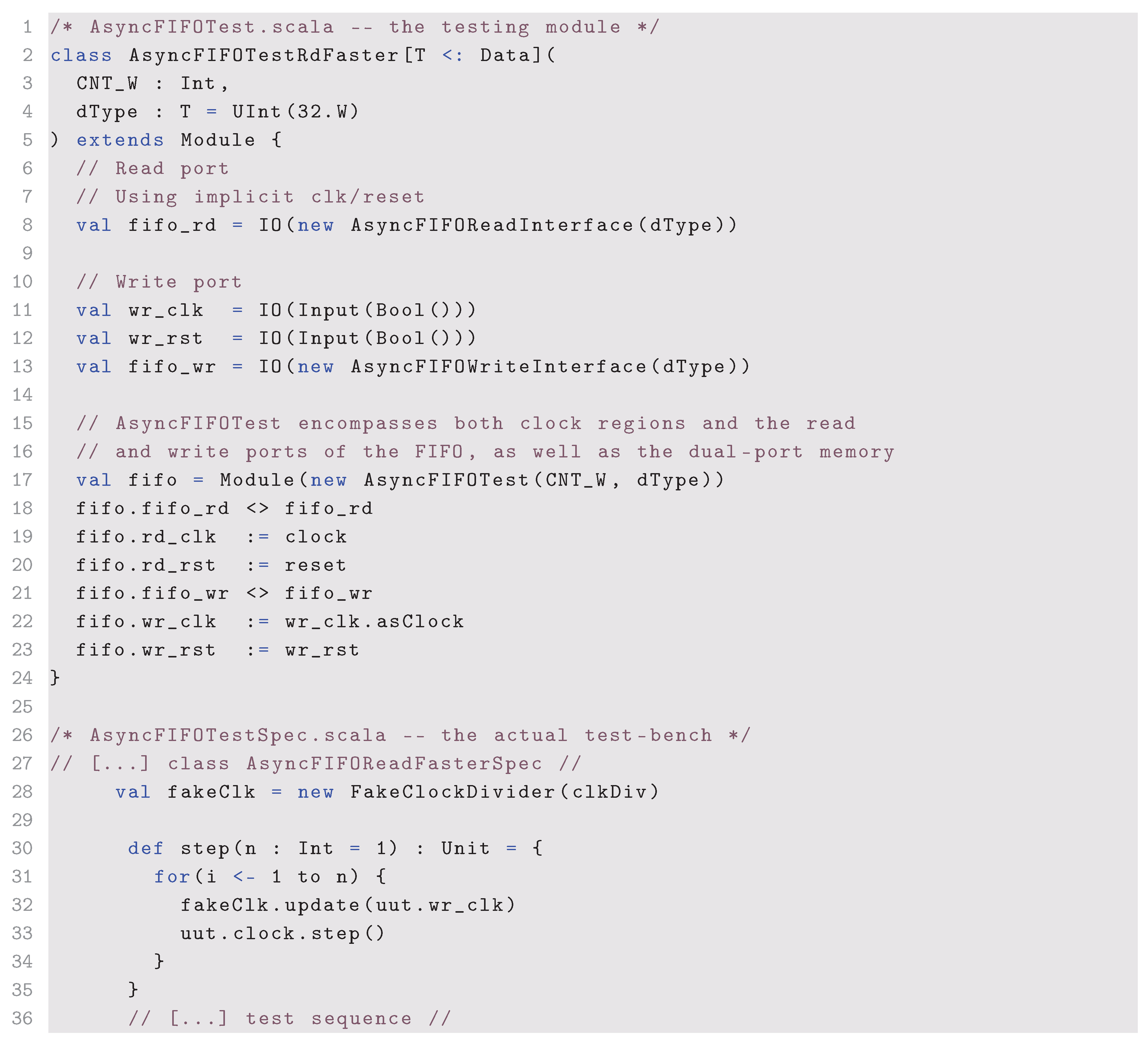 |
In the test sequence defined in the test-bench, all calls to uut.clock.step are replaced by fakeClk.update(uut.wr_clk), which steps the module’s implicit clock and updates the slower wr_clk clock. Figure 11 shows the results of a simulation of the FIFO test-bench, in which the read port is clocked faster than the write port, and catches up the write head, leading to disable the o_nempty signal.
Figure 11.
Asynchronous FIFO test-bench results. The read counter catches up the synchronized write counter in the FIFO read port, leading it to disable its o_nempty signal (solid vertical lines mark the fast clock’s rising edge, while dotted vertical lines mark the slow clock’s rising edge).
Figure 11.
Asynchronous FIFO test-bench results. The read counter catches up the synchronized write counter in the FIFO read port, leading it to disable its o_nempty signal (solid vertical lines mark the fast clock’s rising edge, while dotted vertical lines mark the slow clock’s rising edge).
The major drawback of this testing method is that it doesn’t allow simulating purely asynchronous clocks: the slower clock is always a multiple of the faster one. However, in combination with asynchronous design guidelines and good practices, this testing system has proven suitable for the development of this proof-of-concept.
4. Experimental Results
This section presents the experimental results obtained with the matrix-vector multiplication described in Section 3.1. The results were obtained for each matrix dimension by generating a bitstream, and benchmarking it with a host executable written in C. The host executable generates the requested amount of random matrices and vectors, sends them to the hardware implementation, computes the matrix-vector multiplication in software using the GNU Scientific Library (GSL) [69], and compares the results. It also measures the (software) time taken by both methods.
The bitstreams used for speed and precision benchmarks can be reproduced using make. To generate the benchmark results, each bitstream was tested with the host code, with arguments "-n 100 -m 10 -s 2308555": 10 matrices with 100 vectors each, using random seed 2308555.
Some additional instance sizes were implemented to demonstrate the resource utilization advantages of the proposed framework. Since the clock speed had to be lowered, they were not used for performance benchmarks. The results obtained are presented in Table 1 and Table 2.
4.1. Floating Point Precision
Designs using Berkeley’s hardfloat implementation yielded the exact same results as software floating point operations in the whole benchmark, as reported in Table 1. SAF method showed less precise computing due to the lack of rounding and exception handling, while maintaining acceptable average relative errors.
4.2. Timings and Performance
Since each PE holds two pipeline registers, one coefficient of the input vector takes clock cycles to reach the end of the pipeline. The first coefficient of the result is output once the last PE has received all the coefficients, which is cycles later. All the coefficients are output m cycles after that, so the complete design takes clock cycles to perform a matrix-vector multiplication. This result is valid when the input vector is sent in n cycles, which doesn’t take into account the possible FIFO-induced delays. The ideal use case would be to flood the input FIFO so that it never reaches its empty state, due to the MCP delays in pointer synchronization. Reaching an empty or full FIFO state leads to a delay of several clock cycles.
The presented SAF design was implemented with a 140.625 MHz clock, except for the instances bigger than , which ran at 117.1875 MHz (). The hardfloat implementation could run at for the precision benchmarks. Biggest instances were implemented reducing the clock speed in order to close timing, which is probably due to the lack of intermediate pipelining between PE, especially when crossing SLR using the Super Long Lines.
Hardware and software run times were measured using the C time library. Thus, hardware times measured take into account the syscalls needed to interact with the XDMA. Table 1 shows that hardware becomes faster only for the highest matrix sizes.
4.3. Card Resource Usage
The main contribution of this proof-of-concept is to demonstrate how an RTL-only, complete Chisel codebase can leverage the full capabilities and resources of a high-end accelerator FPGA, such as the Alveo. Table 2 shows that the higher-sized implementations overcome the one-third barrier in resource usage induced by SLR partitioning. While using the golden image would not allow using more than two thirds of the LUT resources, which wouldn’t accomodate the SAF version of the design. Figure 12 shows the biggest implemented designs for both SAF and hardfloat implementations. The figure shows how the full Alveo U200 is occupied by the applicative cores.
5. Discussion
5.1. Floating Point Handling
Berkeley’s hardfloat library implements full-featured floating point operations, including rounding and over- / underflow handling. Thus, the results offer the same precision as standard IEEE-754-compliant floating point units (FPU) such as the one present in the CPU used for software calculations. The custom SAF implementation doesn’t perform rounding on the mantissae, but simply truncates them, which could explain the losses in precision observed in Table 1. SAF precision would be improved with rounding hardware, and further optimized by using guard bits in the SAF mantissae [17].
This implementation however shows how Chisel enables easy conditional templating for handling several variants of the same codebase, using different low-level modules for the same functional behavior.
5.2. Performance
The SAF MAC allowed faster clock frequencies, thanks to its shift-based addition without intermediate normalization or reconversion. However, this is achieved at the expense of resource usage, as can be seen in Table 2. Note that SAF is particularly efficient for dot product and adder tree implementations, and MAC take lesser advantage of SAF particularities [17].
For smaller matrices, the delays induced by driver interactions and clock domain crossings between the rather slow core clock compared and the external 250 MHz bus clock, induce too much overhead to really take advantage of the linear complexity, as can be seen in Table 1. Largest implementations could also gain in timing performance by pipelining the long paths between PE, some of which must cross SLR boundaries using the Super Long Lines.
Moreover, none of the implementations used internal DSP pipelining capabilities: taking advantage of this feature could improve the overall limiting clock period by shortening the combinational paths, especially.
5.3. Resource Usage
Table 2 shows how the Vivado synthesis tool optimizes the memory management by switching from distributed random access memory based on LUT (LUTRAM) to RAM and Ultra RAM blocks (not detailed in Table 2) when the number of coefficients to store in each PE reaches a certain threshold. The limiting resource in both designs is the number of storage elements for PE memories: depending on the height (number of PE) and width (number of coefficients to store in each PE) of the matrix, RAM blocks may come short in which case LUTRAM are used to complete the missing memory capacity, but this limits the amount of LUT available for logic.
5.4. Proof-of-Concept Objectives
The proposed framework proved useful for creating a subordinate hardware accelerator, at the register transfer level. Its key features are :
- Reusable: module encapsulation allows reusing parts of the design like FIFO, MCP, or even the AXI stack, in other designs
- Real-life enabled: multi-clock designs on complex FPGA architectures can be useful to prototype ASIC designs
- Fully controllable: the designer has RTL control over the hardware and syscall level control over the software. Moreover, all card resources are available for use.
- Platform-agnostic: Any Linux-based OS supporting the basic dependencies of the project can run matmul.
6. Conclusions and Future Research
This proof-of-concept demonstrates a full-RTL framework, that allows implementing hardware accelerators on the high-end, multi-SLR AMD / Xilinx Alveo FPGA, using the Chisel language. Allowing multi-clock designs, with reusable modules and wrappers following good practice design guidelines, the matmul [19] project aims to provide designers with a good starting point for multi-SLR, real-life design or prototyping for UltraScale+ FPGA architecture that require RTL control over the whole programmable logic implementation.
Targeted to Alveo, the framework drops high-level design methods such as HLS, that can become hard to use for specific hardware requirements. It also gets rid of the Alveo golden image which takes approximately one third of the available resources on the Alveo U200. In addition to fully exploit the large amounts of resources present on the FPGA, this framework thus also allows developing host code in plain C, without the need to install Xilinx runtime libraries, that are supported by very few Linux distributions.
On the downside of the presented framework, the core is bound to function as a subordinate to the PCIe bus (and thus the host CPU). However, a custom PCIe driver could be implemented to react to the card’s requests, and the XDMA could be configured in AXI-PCIe bridge mode to support transmitting master requests from the FPGA board. This would call for AXI-master module development, and could then enable direct PCIe access from programmable logic (PL), allowing designers to create any kind of hybrid system based on the UltraScale+ FPGA architecture. In conclusion, using the same workflow for designing a PCIe controller with DMA capabilities is possible, but at the expense of implementing AXI4 master controllers and a host-side PCIe driver. All the clock domain crossing methods and the general high-level design layout would be the same.
Author Contributions
Conceptualization, R.G. and T.O.B; methodology, R.G. and T.O.B; software, R.G.; validation, R.G.; formal analysis, R.G. and T.O.B; investigation, R.G. and T.O.B; resources, R.G. and T.O.B; data curation, R.G.; writing—original draft preparation, R.G. and T.O.B; writing—review and editing, R.G. and T.O.B; visualization, R.G.; supervision, T.O.-B. All authors have read and agreed to the published version of the manuscript.
Funding
This research was funded in part by the NSERC Discovery grants program. The grant numbers are RGPIN-2021-03935.
Conflicts of Interest
The authors declare no conflicts of interest.
References
- Hernandez, J.; et al. Field Programmable Gate Array: An Extensive Review, Recent Trends, Challenges, and Applications. Computation 2019, 7, 63.
- Society, I.C. The Role of Field-Programmable Gate Arrays in the Acceleration of Scientific Computing. IEEE Computer 2024, 57, 45–53.
- AMD/Xilinx. UltraScale Architecture and Product Data Sheet: Overview, 2025. v4.7.
- Du, L.; Liang, T.; Zhou, X.; Ge, J.; Li, S.; Sinha, S.; Zhao, J.; Xie, Z.; Zhang, W. FADO: Floorplan-Aware Directive Optimization Based on Synthesis and Analytical Models for High-Level Synthesis Designs on Multi-Die FPGAs. ACM Trans. Reconfigurable Technol. Syst. 2024, 17.
- Uguen, Y.; Dinechin, F.D.; Lezaud, V.; Derrien, S. Application-Specific Arithmetic in High-Level Synthesis Tools. ACM Trans. Archit. Code Optim. 2020, 17.
- Cong, J.; Lau, J.; Liu, G.; Neuendorffer, S.; Pan, P.; Vissers, K.; Zhang, Z. FPGA HLS Today: Successes, Challenges, and Opportunities. ACM Trans. Reconfigurable Technol. Syst. 2022, 15.
- AMD. Xilinx Runtime (XRT). https://xilinx.github.io/XRT, 2023. [Accessed: 2025-06-01].
- Sahebi, A.; Barbone, M.; Procaccini, M.; Luk, W.; Gaydadjiev, G.; Giorgi, R. Distributed large-scale graph processing on FPGAs. Journal of Big Data 2023, 10, 95.
- Sozzo, E.D.; Conficconi, D.; Zeni, A.; Salaris, M.; Sciuto, D.; Santambrogio, M.D. Pushing the Level of Abstraction of Digital System Design: A Survey on How to Program FPGAs. ACM Comput. Surv. 2022, 55.
- chipsalliance. Chisel homepage. https://www.chisel-lang.org. [Accessed: 2025-05-29].
- Schoeberl, M.; Damsgaard, H.J.; Pezzarossa, L.; Keszocze, O.; Jellum, E.R. Hardware Generators with Chisel. In Proceedings of the Euromicro Conference on Digital System Design (DSD), 2024, pp. 168–175.
- Käyrä, M.; Hämäläinen, T.D. A Survey on System-on-a-Chip Design Using Chisel HW Construction Language. In Proceedings of the Annual Conference of the IEEE Industrial Electronics Society (IECON), 2021, pp. 1–6.
- AMD. DMA/Bridge Subsystem for PCI Express (XDMA) v4.1 - Product Guide PG195. https://docs.xilinx.com/r/en-US/pg195-pcie-dma, 2023. [Accessed: 2025-06-01].
- IEEE Computer Society. IEEE Standard for Verilog Hardware Description Language (IEEE Std 1364-2001). https://standards.ieee.org/standard/1364-2001.html, 2001. [Accessed: 2025-06-01].
- edwardcwang. decoupled-serializer. https://github.com/edwardcwang/decoupled-serializer, 2025.
- Arm Ltd.. AMBA AXI and ACE Protocol Specification (AXI3, AXI4, AXI4-Lite). https://developer.arm.com/documentation/ihi0022/e, 2022. [Accessed: 2025-06-01].
- Ould-Bachir, T.; David, J.P. Self-Alignment Schemes for the Implementation of Addition-Related Floating-Point Operators. ACM Trans. Reconfigurable Technol. Syst. 2013, 6.
- AMD. Alveo U200 Data Center Accelerator Card. https://www.amd.com/en/products/accelerators/alveo-u200, 2023. [Accessed: 2025-06-01].
- Robin Gay (RobinGTM). matmul. https://github.com/RobinGTM/matmul/tree/v1.0-mdpi, 2025. [Public repository].
- AMD. AMD Alveo Adaptable Accelerator Cards. https://www.amd.com/en/products/accelerators/alveo.html, 2025. [Accessed: 2025-06-02].
- AMD. UltraScale Architecture Clocking Resources User Guide, 2025. 1.11 English.
- Saban, K. Xilinx Stacked Silicon Interconnect Technology Delivers Breakthrough FPGA Capacity, Bandwidth, and Power Efficiency. Technical Report WP380, Xilinx, 2012. v1.2.
- AMD/Xilinx. UltraFast Design Methodology Guide for FPGAs and SoCs, 2024. 2024.2 English.
- AMD/Xilinx. Alveo U200 and U250 Accelerator Cards User Guide, 2023. 1.1 English.
- AMD/Xilinx. Alveo Data Center Accelerator Card Platforms User Guide, 2023. 2.0.1 English.
- AMD. Pynq homepage. https://www.pynq.io/, 2024. [Accessed: 2025-06-02].
- Xilinx. Alveo U200 and U250 Data Center Accelerator Cards Data Sheet, 2023. v1.7 English.
- AMD/Xilinx. Xilinx Runtime (XRT) Release Notes, 2024. 2024.2 English.
- AMD/Xilinx. Vitis Tutorials: Hardware Acceleration, 2025. 2024.2 English.
- Gisselquist Technology, L. Building and AXI-Lite slave the easy way. https://zipcpu.com/blog/2020/03/08/easyaxil.html, 2020. [Accessed: 2025-06-02].
- AMD/Xilinx. Data Center Acceleration Using Vitis User Guide, 2025. 2024.2 English.
- Xilinx. DMA/Bridge Subsystem for PCI Express v4.1 Product Guide, 2022. v4.1.
- Xilinx. dma_ip_drivers. https://github.com/Xilinx/dma_ip_drivers.git, 2025. [Accessed: 2025-06-02].
- Schoeberl, M. Digital Design with Chisel; Kindle Direct Publishing, 2019.
- Izraelevitz, A.; Koenig, J.; Li, P.; Lin, R.; Wang, A.; Magyar, A.; Kim, D.; Schmidt, C.; Markley, C.; Lawson, J.; et al. Reusability is FIRRTL ground: Hardware construction languages, compiler frameworks, and transformations. In Proceedings of the 2017 IEEE/ACM International Conference on Computer-Aided Design (ICCAD), Nov 2017, pp. 209–216. https://doi.org/10.1109/ICCAD.2017.8203780.
- Li, P.S.; Izraelevitz, A.M.; Bachrach, J. Specification for the FIRRTL Language. Technical Report UCB/EECS-2016-9, EECS Department, University of California, Berkeley, 2016.
- chipsalliance. chisel. https://github.com/chipsalliance/chisel, 2025. [Accessed: 2025-06-27].
- chipsalliance. Chisel documentation homepage. https://www.chisel-lang.org/docs. [Accessed: 2025-06-27].
- chipsalliance. svsim. https://github.com/chipsalliance/chisel/tree/main/svsim, 2025. [Accessed: 2025-06-27].
- chipsalliance. Motivation – "Why Chisel?". https://www.chisel-lang.org/docs/explanations/motivation. [Accessed: 2025-06-27].
- chipsalliance. Multiple Clock Domains. https://www.chisel-lang.org/docs/explanations/multi-clock. [Accessed: 2025-06-27].
- Center, S. Scala Build Tool homepage. https://www.scala-sbt.org/, 2025. [Accessed: 2025-07-07].
- Veripool. Verilator homepage. https://www.veripool.org/verilator/, 2024. [Accessed: 2025-06-27].
- ucb bar. chiseltest. https://github.com/ucb-bar/chiseltest, 2024. [Accessed: 2025-06-27].
- edwardcwang. decoupled-serializer. https://github.com/RobinGTM/decoupled-serializer, 2025.
- IEEE Standard for Floating-Point Arithmetic. IEEE Std 754-2008 2008, pp. 1–70.
- Muller, J.M.; Brunie, N.; de Dinechin, F.; Jeannerod, C.P.; Joldes, M.; Lefèvre, V.; Melquiond, G.; Revol, N.; Torres, S. Handbook of Floating-point Arithmetic (2nd edition); Birkhäuser Basel, 2018; pp. 1–627. [CrossRef]
- ucb bar. berkeley-hardfloat. https://github.com/ucb-bar/berkeley-hardfloat, 2023. [Accessed: 2025-06-27].
- de Dinechin, F.; Pasca, B.; Creţ, O.; Tudoran, R. An FPGA-specific approach to floating-point accumulation and sum-of-products. 2008 International Conference on Field-Programmable Technology 2008, pp. 33–40.
- Luo, Z.; Martonosi, M. Accelerating pipelined integer and floating-point accumulations in configurable hardware with delayed addition techniques. IEEE Transactions on Computers 2000, 49, 208–218. [CrossRef]
- Vangal, S.; Hoskote, Y.; Borkar, N.; Alvandpour, A. A 6.2-GFlops Floating-Point Multiply-Accumulator With Conditional Normalization. IEEE Journal of Solid-State Circuits 2006, 41, 2314–2323. [CrossRef]
- Hajizadeh, F.; Ould-Bachir, T.; David, J.P. CuFP: An HLS Library for Customized Floating-Point Operators. Electronics 2024, 13.
- Hauser, J. Berkeley HardFloat. https://www.jhauser.us/arithmetic/HardFloat.html, 2024.
- AMBA AXI-Stream Protocol Specification. Technical Report ARM IHI 0051B (ID040921), 2021.
- Wikipedia contributors. Metastability (electronics) — Wikipedia, The Free Encyclopedia, 2025. [Accessed: 2025-08-11].
- Ginosar, R. Metastability and Synchronizers: A Tutorial. IEEE Design & Test of Computers 2011, 28, 23–35. [CrossRef]
- Stephenson, J.; Chen, D.; Fung, R.; Chromczak, J. White Paper – Understanding metastability in FPGAs. Technical Report WP-01082-1.2, Altera Corporation, 2009. ver. 1.2.
- Golson, S. Synchronization and Metastability. In Proceedings of the SNUG Silicon Valley 2014. Trilobyte Systems, 2014. [Accessed: 2025-07-04].
- Cummings, C.E. Clock Domain Crossing (CDC) Design & Verification Techniques Using SystemVerilog. In Proceedings of the SNUG Boston 2008. Sunburst Design, Inc., 2008.
- Cummings, C.E. Simulation and Synthesis Techniques for Asynchronous FIFO Design. In Proceedings of the SNUG San Jose 2002. Sunburst Design, Inc., 2002. [Accessed: 2025-06-01].
- Gray, F. Pulse code communication. Technical Report US2632058A, United States Patent Office, 1947.
- vineetskumar. XDMA tests failing with Error 512 on Alveo U200 #331. https://github.com/Xilinx/dma_ip_drivers/pull/240, 2025. [Accessed: 2025-08-11].
- eniv. [XDMA] BUG: scheduling while atomic in engine_service_poll #229. https://github.com/Xilinx/dma_ip_drivers/issues/229, 2023. [Accessed: 2025-08-11].
- GitSoftwareNow. The XDMA did not work when I send big buffer #298. https://github.com/Xilinx/dma_ip_drivers/issues/298, 2024. [Accessed: 2025-08-11].
- mpb27. XDMA: End of packet has issues and needs more testing. #91. https://github.com/Xilinx/dma_ip_drivers/issues/91#issuecomment-2316828753, 2020. [Accessed: 2025-08-11].
- dwd_pete. C2H Streaming XDMA Linux Driver Broken. https://adaptivesupport.amd.com/s/question/0D52E00006hpgSoSAI/c2h-streaming-xdma-linux-driver-broken?language=en_US, 2018. [Accessed: 2025-08-11].
- AMBA AXI and ACE Protocol Specification. Technical Report ARM IHI 022D (ID102711), 2011. AXI3, AXI4, and AXI4-Lite ACE and ACE-Lite.
- chipsalliance. Chisel Multiple Clock Domains documentation. https://www.chisel-lang.org/docs/explanations/multi-clock. [Accessed: 2025-07-08].
- The GSL Team. GNU Scientific Library homepage. https://www.gnu.org/software/gsl/, 2024. [Accessed: 2025-07-12].
- The Free Software Foundation, I. GNU General Public License. https://www.gnu.org/licenses/gpl-3.0.en.html, 2007. [Accessed: 2025-08-11].
Figure 2.
High-level schematics.
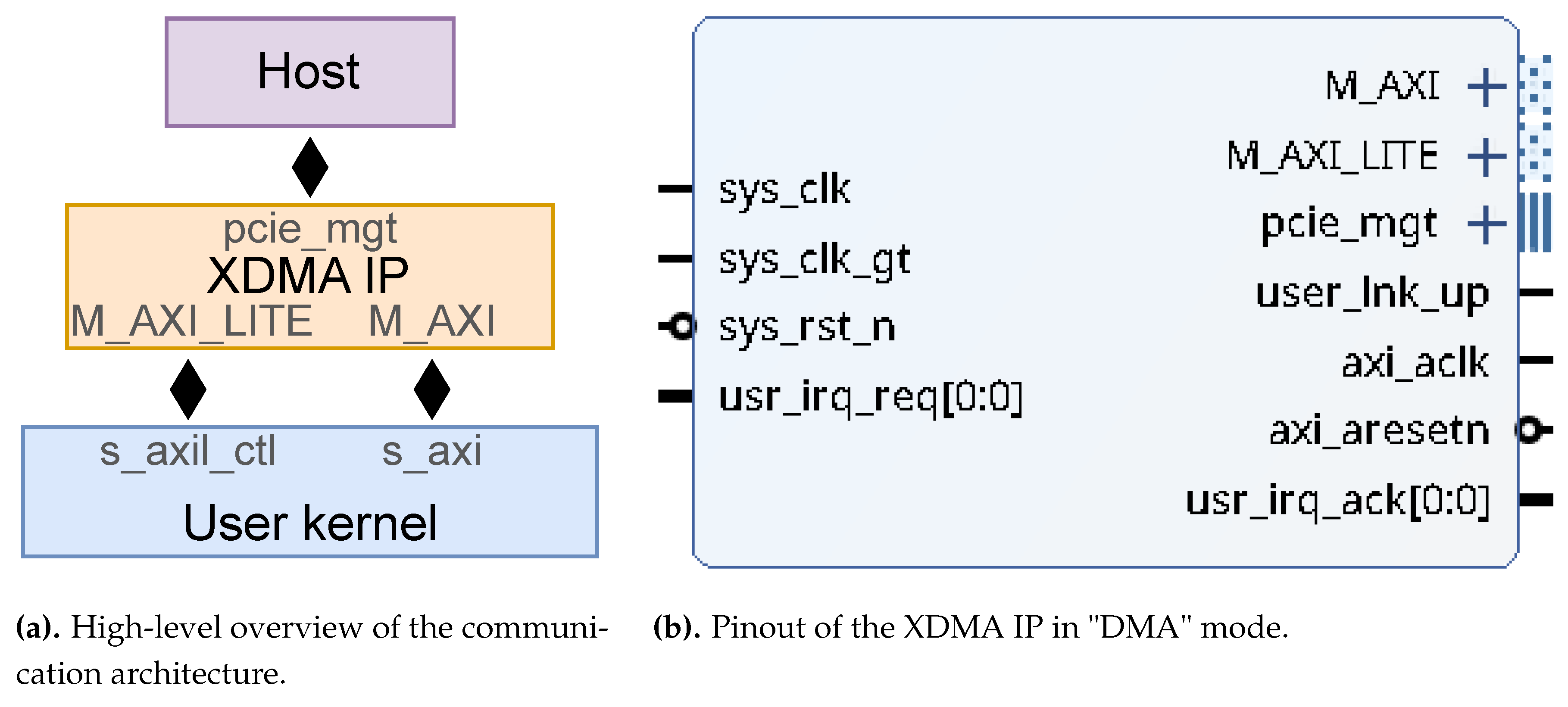
Figure 3.
Chisel workflow, from a Scala file to waveform file or Verilog file (adapted from [34,37,38,39]).
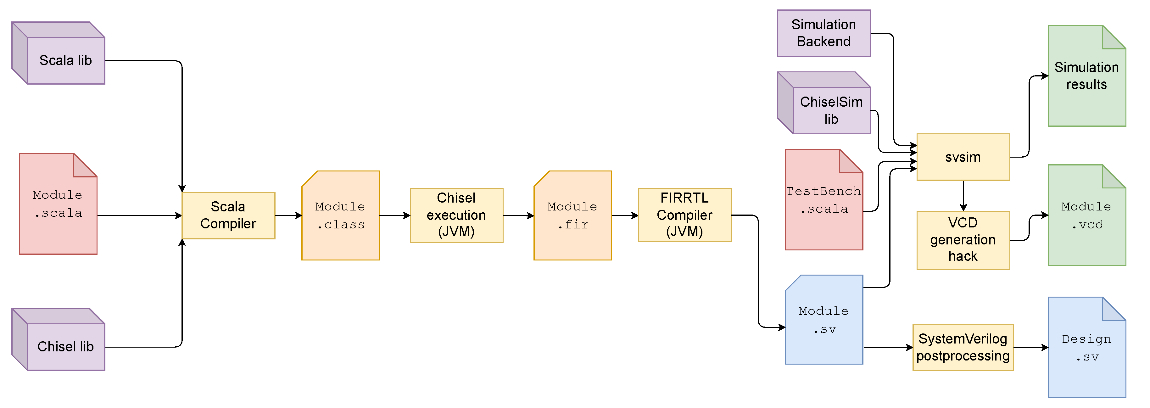
Figure 4.
Floating point formats used in the implementations. From top to bottom: standard IEEE-754 binary32; "recoded" or "expanded" floats; self-aligned format with and .
Figure 4.
Floating point formats used in the implementations. From top to bottom: standard IEEE-754 binary32; "recoded" or "expanded" floats; self-aligned format with and .
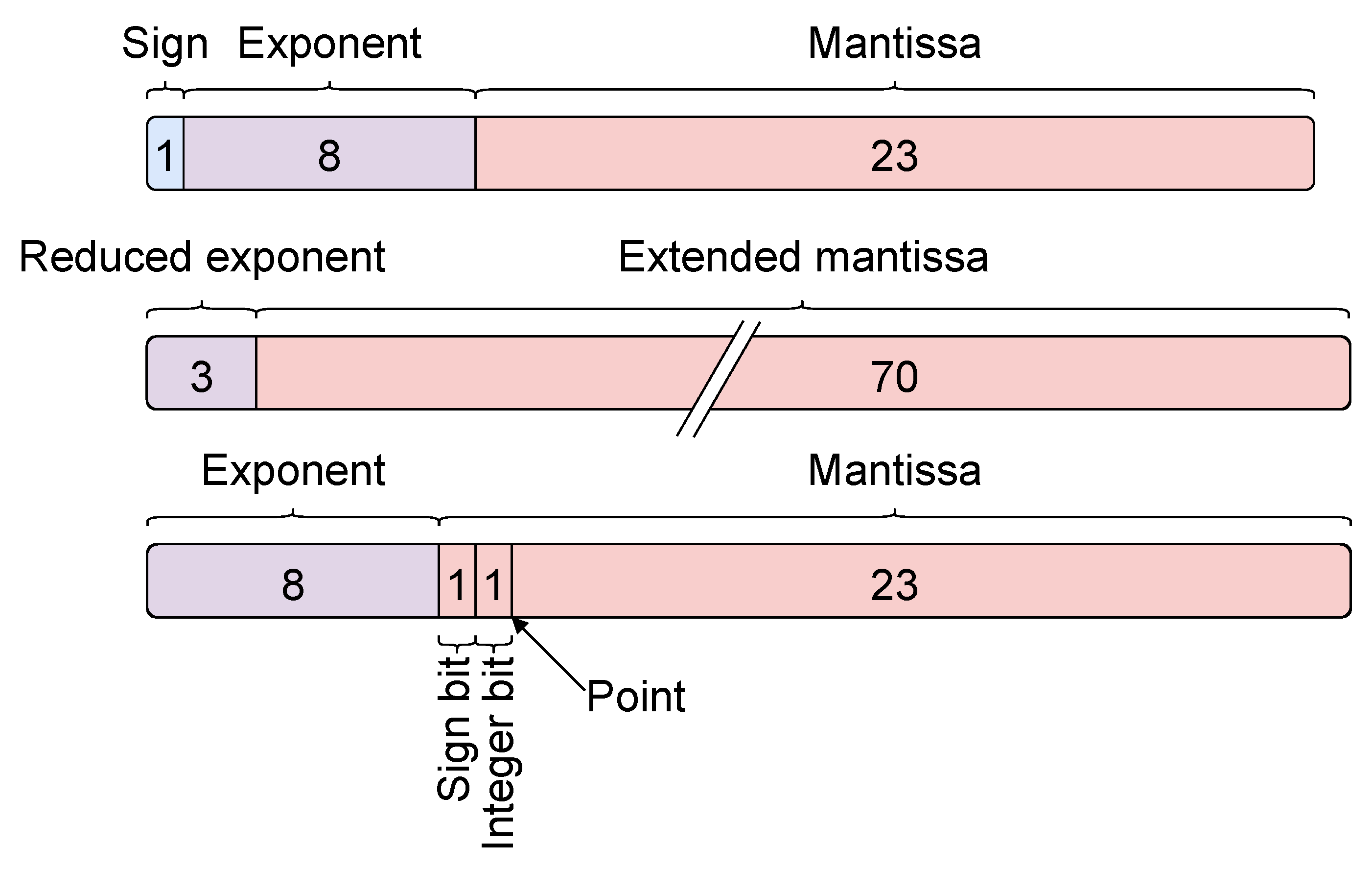
Figure 5.
Pipelined MAC present in each processing element. The SAF or hardfloat floating point implementation can be chose at compile-time.
Figure 5.
Pipelined MAC present in each processing element. The SAF or hardfloat floating point implementation can be chose at compile-time.
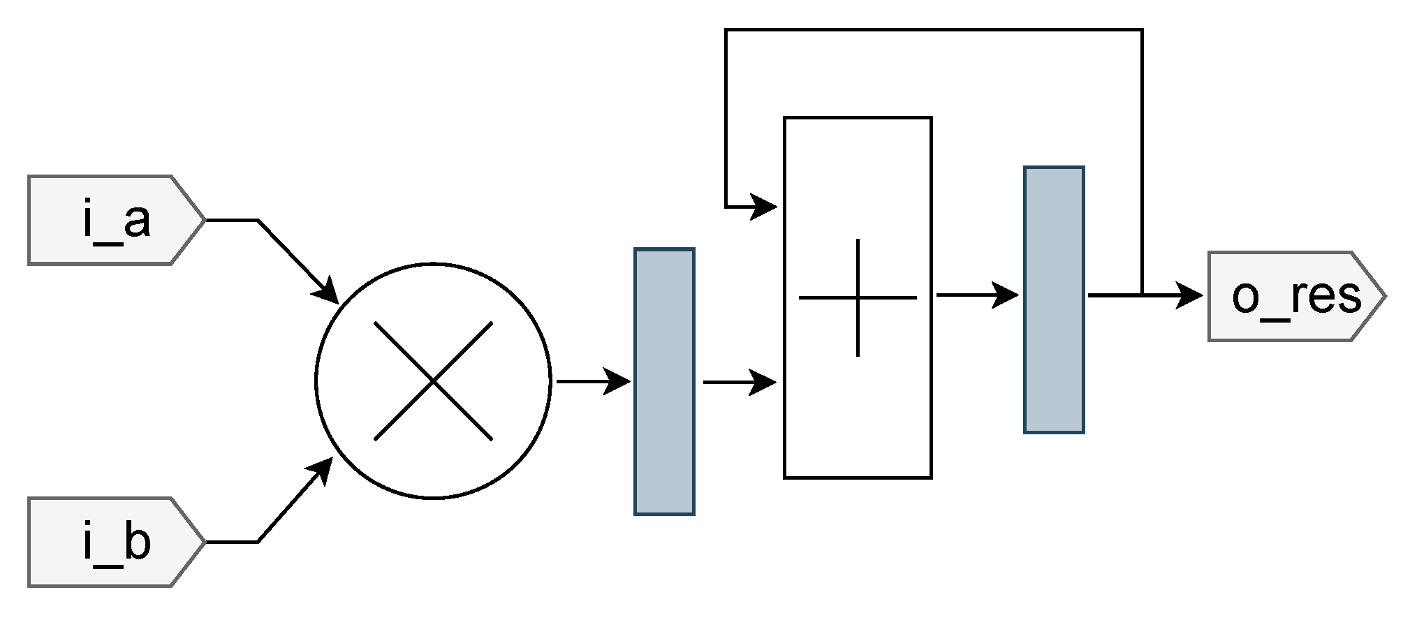
Figure 7.
Undesirable metastability phenomena and synchronization mechanism. Metastability can lead to wrong value interpretation, potentially generating either wrong, delayed or even impossible state transitions. (Legend: ts: setup time; th: hold time; tp: internal FF propagation time; tl: logic propagation time; ↑: sampling clock edge. Dotted lines represent potentially metastable datapaths, purple lines represent clock domain crossing paths, and black lines safe paths).
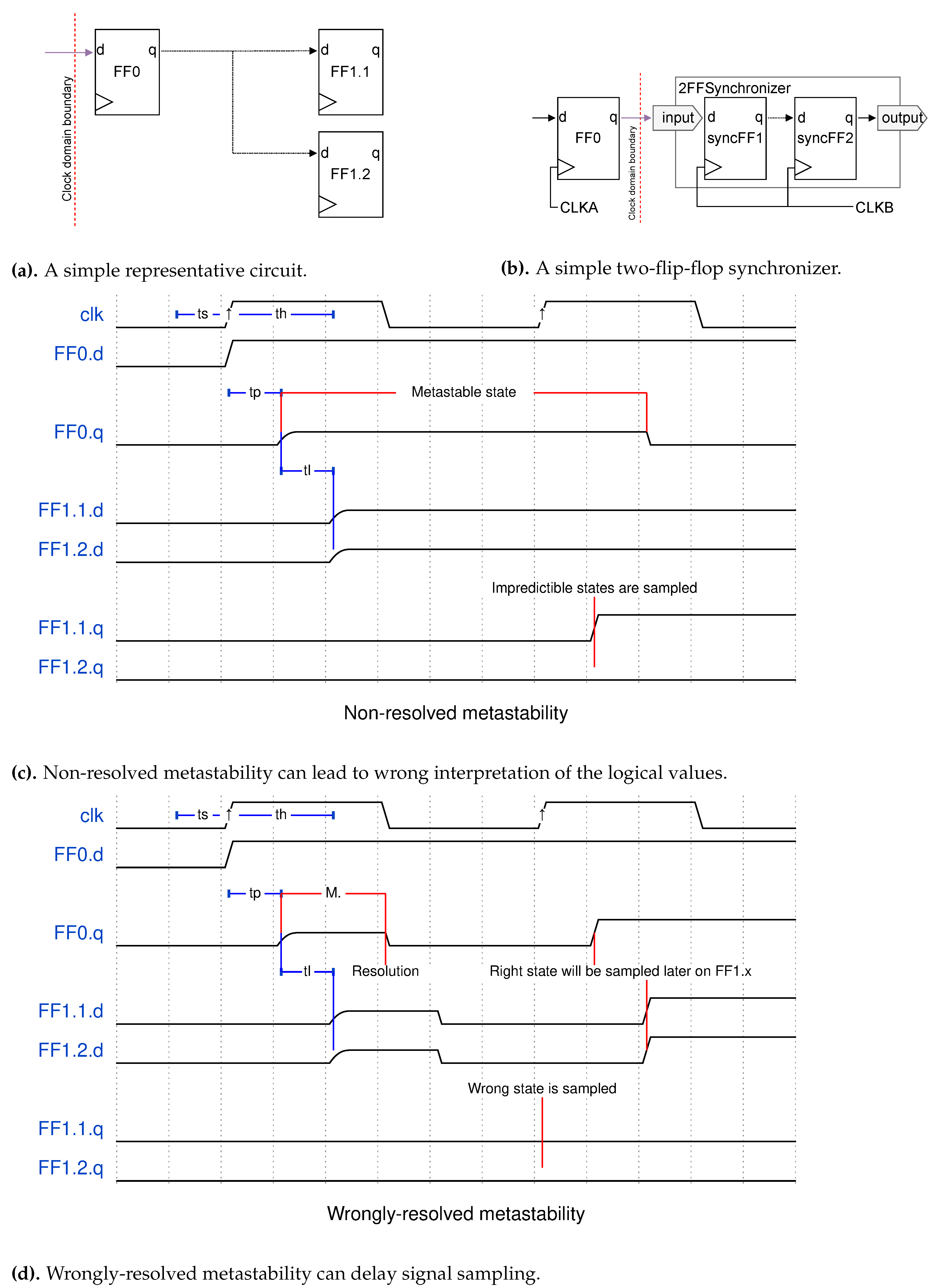
Figure 8.
Multi-cycle path source and destination modules allow to safely cross a clock domain boundary, even when the data payload is several bits wide (src stands for "source" and dst for "destination").
Figure 8.
Multi-cycle path source and destination modules allow to safely cross a clock domain boundary, even when the data payload is several bits wide (src stands for "source" and dst for "destination").
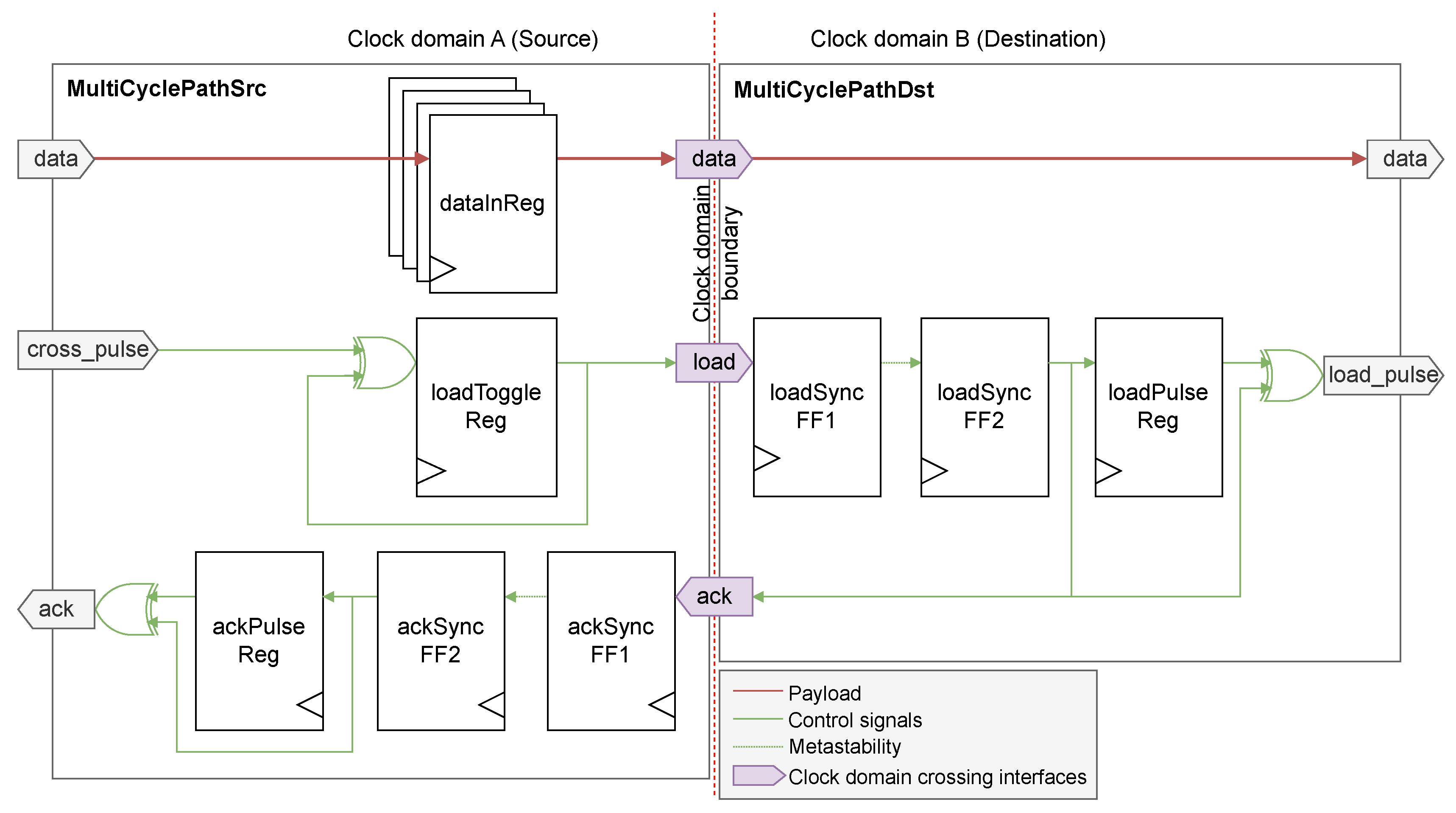
Figure 12.
XCU200 FPGA occupation for the biggest implemented designs. The XDMA cells are highlighted in magenta, while the AXIWrapper cells are in light green, and the input and output FIFO in yellow. The remaining cells (in cyan) are used by the CoreWrapper module.
Figure 12.
XCU200 FPGA occupation for the biggest implemented designs. The XDMA cells are highlighted in magenta, while the AXIWrapper cells are in light green, and the input and output FIFO in yellow. The remaining cells (in cyan) are used by the CoreWrapper module.
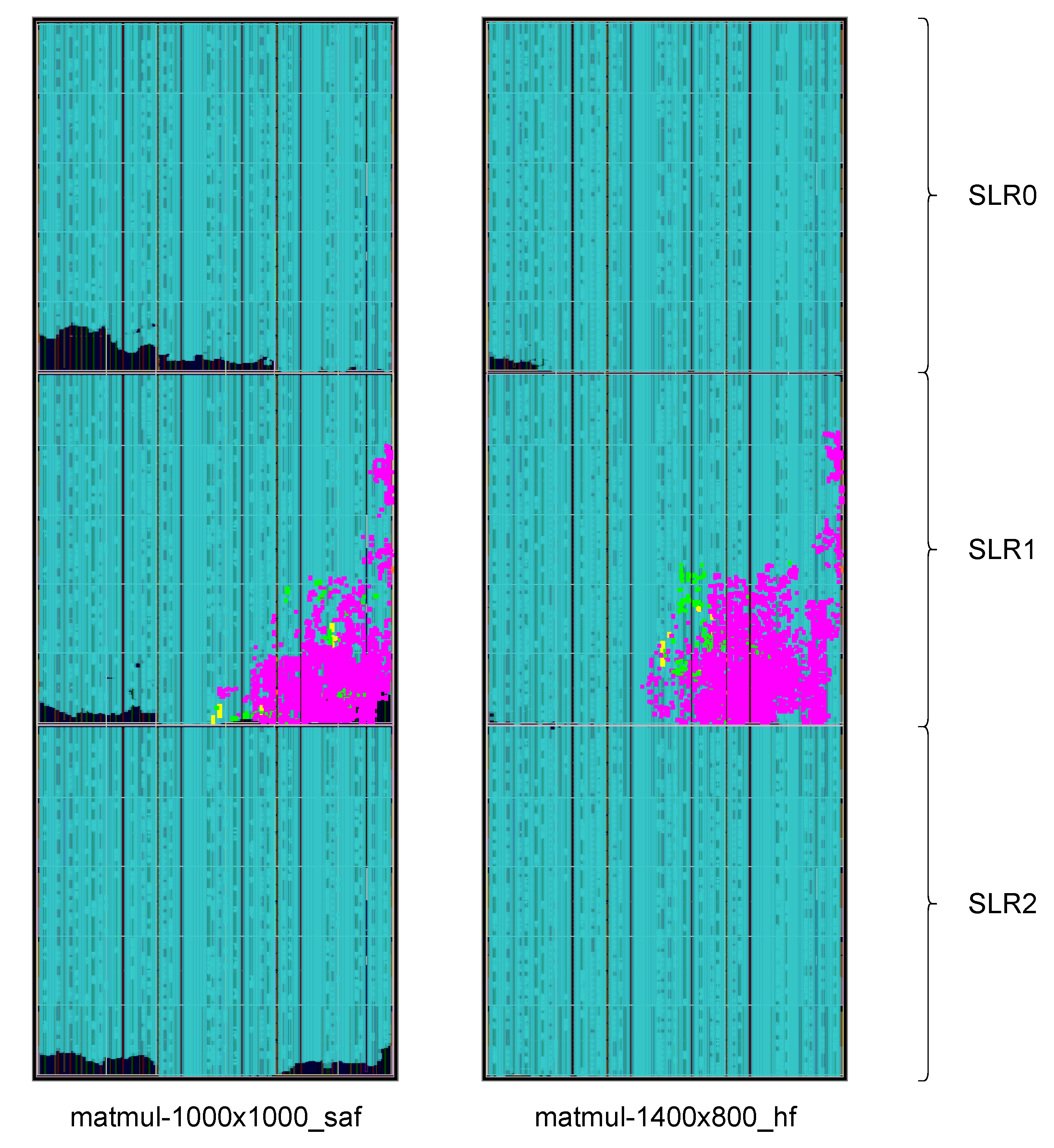

Table 1.
Precision and timing results. MH and MW are the matrix height and width, respectively. Note that MH corresponds to the number of PE, while MW is the depth of each PE’s memory. FP shows the floating point implementation used: SAF or hardfloat (HF). Errors are computed relatively to the input vector’s euclidian norm.
| MH | MW | FP | Hardware time (ms) | Software time (ms) | Relative error (%) | |||
| Mean | Max | Mean | Max | Mean | Max | |||
| 10 | 10 | SAF | 0.031937 | 0.077000 | 0.000950 | 0.016000 | 0.000274 | 0.003808 |
| 50 | 50 | SAF | 0.023638 | 0.129000 | 0.002490 | 0.031000 | 0.004407 | 0.075721 |
| 100 | 50 | SAF | 0.025186 | 0.073000 | 0.004631 | 0.020000 | 0.012710 | 1.165867 |
| 100 | 100 | SAF | 0.022483 | 0.123000 | 0.008745 | 0.039000 | 0.039777 | 6.425782 |
| 100 | 200 | SAF | 0.025268 | 0.175000 | 0.020996 | 0.096000 | 0.027460 | 4.977176 |
| 300 | 300 | SAF | 0.016123 | 0.090000 | 0.048481 | 0.210000 | 0.126155 | 18.62970 |
| 400 | 400 | SAF | 0.013933 | 0.058000 | 0.072135 | 0.258000 | 0.312330 | 50.52832 |
| 10 | 10 | HF | 0.026675 | 0.094000 | 0.000827 | 0.112000 | 0.000000 | 0.000000 |
| 50 | 50 | HF | 0.030913 | 0.171000 | 0.003696 | 0.134000 | 0.000000 | 0.000000 |
| 100 | 50 | HF | 0.023033 | 0.117000 | 0.005115 | 0.042000 | 0.000000 | 0.000000 |
| 100 | 100 | HF | 0.023357 | 0.103000 | 0.008535 | 0.042000 | 0.000000 | 0.000000 |
| 100 | 200 | HF | 0.021130 | 0.117000 | 0.016658 | 0.068000 | 0.000000 | 0.000000 |
| 300 | 300 | HF | 0.014292 | 0.052000 | 0.042206 | 0.205000 | 0.000000 | 0.000000 |
| 400 | 400 | HF | 0.015355 | 0.078000 | 0.080186 | 0.346000 | 0.000000 | 0.000000 |
Table 2.
Resource utilization results. The yellow row indicates resource counts and percentages left after subtracting the golden image’s resources, according to UG1120 [25].
Table 2.
Resource utilization results. The yellow row indicates resource counts and percentages left after subtracting the golden image’s resources, according to UG1120 [25].
| MH | MW | FP | LUT | FF | BRAM | DSP | ||||
| Count | % | Count | % | Count | % | Count | % | |||
| Golden image (left resources) | 978000 | 82.72 | 1956000 | 82.72 | 1860 | 86.11 | 5880 | 85.96 | ||
| 10 | 10 | S | 22437 | 1.898 | 16889 | 0.7143 | 33 | 1.528 | 20 | 0.2924 |
| 50 | 50 | S | 69384 | 5.869 | 27162 | 1.149 | 35 | 1.620 | 100 | 1.462 |
| 100 | 50 | S | 128222 | 10.85 | 40141 | 1.698 | 35 | 1.620 | 200 | 2.924 |
| 100 | 100 | S | 133661 | 11.31 | 40355 | 1.707 | 35 | 1.620 | 200 | 2.924 |
| 100 | 200 | S | 144255 | 12.21 | 40564 | 1.716 | 35 | 1.620 | 200 | 2.924 |
| 300 | 200 | S | 410972 | 34.77 | 94354 | 3.991 | 36 | 1.667 | 600 | 8.772 |
| 300 | 300 | S | 363067 | 25.86 | 92316 | 3.904 | 337 | 15.60 | 600 | 8.771 |
| 400 | 400 | S | 472903 | 40.00 | 117767 | 4.981 | 437 | 20.23 | 800 | 11.70 |
| 800 | 800 | S | 925654 | 78.30 | 224181 | 9.481 | 839 | 38.84 | 1600 | 23.39 |
| 900 | 900 | S | 1042003 | 88.14 | 250384 | 10.59 | 941 | 43.56 | 1800 | 26.32 |
| 1000 | 1000 | S | 1115257 | 97.44 | 276586 | 11.70 | 1041 | 48.19 | 2000 | 29.24 |
| 10 | 10 | H | 19122 | 1.618 | 16080 | 0.6802 | 33 | 1.528 | 20 | 0.2924 |
| 50 | 50 | H | 51927 | 4.393 | 23094 | 0.9767 | 35 | 1.620 | 100 | 1.462 |
| 100 | 50 | H | 93263 | 7.889 | 32004 | 1.354 | 35 | 1.620 | 200 | 2.924 |
| 100 | 100 | H | 98566 | 8.339 | 32215 | 1.363 | 35 | 1.620 | 200 | 2.924 |
| 100 | 200 | H | 108816 | 9.205 | 32426 | 1.372 | 35 | 1.620 | 200 | 2.924 |
| 300 | 200 | H | 305556 | 25.85 | 70048 | 2.963 | 36 | 1.667 | 600 | 8.772 |
| 300 | 300 | H | 246760 | 21.01 | 68017 | 2.923 | 337 | 15.60 | 600 | 8.771 |
| 400 | 400 | H | 324692 | 27.46 | 85764 | 3.627 | 437 | 20.23 | 800 | 11.70 |
| 800 | 800 | H | 644338 | 54.50 | 160182 | 6.775 | 841 | 38.94 | 1600 | 23.39 |
| 1000 | 1000 | H | 802580 | 67.89 | 196585 | 8.314 | 1041 | 48.19 | 2000 | 29.24 |
| 1200 | 800 | H | 960472 | 81.24 | 236592 | 10.01 | 1245 | 57.64 | 2400 | 35.09 |
| 1300 | 700 | H | 1040130 | 87.98 | 255090 | 10.79 | 1345 | 62.27 | 2600 | 38.01 |
| 1400 | 800 | H | 1119565 | 94.70 | 273582 | 11.57 | 1445 | 66.90 | 2800 | 40.94 |
Disclaimer/Publisher’s Note: The statements, opinions and data contained in all publications are solely those of the individual author(s) and contributor(s) and not of MDPI and/or the editor(s). MDPI and/or the editor(s) disclaim responsibility for any injury to people or property resulting from any ideas, methods, instructions or products referred to in the content. |
© 2025 by the authors. Licensee MDPI, Basel, Switzerland. This article is an open access article distributed under the terms and conditions of the Creative Commons Attribution (CC BY) license (http://creativecommons.org/licenses/by/4.0/).
Copyright: This open access article is published under a Creative Commons CC BY 4.0 license, which permit the free download, distribution, and reuse, provided that the author and preprint are cited in any reuse.


