Submitted:
12 August 2025
Posted:
13 August 2025
You are already at the latest version
Abstract
Nanoscale pentacene-based organic field-effect transistors (OFETs) incorporating a triple insulating layer of polymethyl methacrylate (PMMA), silicon dioxide (SiO2), and zinc ox-ide (ZnO) were successfully fabricated on glass and flexible PET substrates. The insulating layers significantly enhanced device performance, with the OFETs achieving field-effect mobility (µ) values more than twice as high as those reported in the literature. Specifically, mobility of ~6.75 cm²/V·s on glass, ~7.141 cm²/V·s on flexible substrates (before bending), and ~6.88 cm²/V·s (after bending) were observed. Threshold voltages (Vth) of -7 V and -9 V were estimated for the flexible OFETs before and after bending, respectively, alongside a high on/off current ratio exceeding 10³ for all devices. Minimal hysteresis in the transfer and output characteristics indicated excellent, trap-free interaction between the insulating layers and the pentacene. The high dielectric constant of the PMMA/SiO2/ZnO triple insu-lating layers was identified as a critical factor driving the exceptional performance, stabil-ity, and low hysteresis of the OFETs. These results underscore the pivotal role of advanced insulating layers in optimizing OFET performance and durability.
Keywords:
flexible device
; nanoscale
; organic filed effect transistor
; triple insulator layers
1. Introduction
Flexible electronics is the name given to a family of thin-film electronic devices that have high electrical performance, dependability, and the capacity to be bent, squeezed, stretched, folded, and even twisted into strange forms. Flexible organic electrical arrays integrate harmoniously with biological systems, resulting in a wide range of human-friendly applications, including smart prosthetics and electronic skins [1] and wearable technology for tracking health and human activity [2]. The qualities that trade-off between device flexibility and best electronic properties were the main area of concern for organic flexible electronics [3]. Because organic materials are naturally flexible, they can be used on flexible substrates without losing their electrical properties or becoming stressed out [4,5]. This has allowed improving of the latest generation of electronics to rely on small molecular component, or polymers. Both academic and industrial researchers are interested in these devices [6,7] due to their mechanical flexibility, low temperature processing, and cheapness [3,6,7]. Recently, several research groups have used organic material in the design of various flexible electronic devices, as such, organic solar cells [8,9], light emitting displays [10,11], sensors [8,12], memories [13,14], organic flexible integrated circuits [3], and organic field-effect transistors [15,16] all of which are at a fairly advanced level of research.
Recent research in nanoscale organic electronics has concentrated on substituting flexible substrates like metallic foils or plastic for the conventional rigid glass plate substrate [8,12,17]. There are a wide range of soft substrates that are suitable for fabricated the flexible electronic devices, including plastics (e.g., polyethylene-2,6-naphthalate (PEN), poly(ethylene terephthalate) (PET), parylene), fibre (textiles), papers, and elastomers (e.g., polyimide (PI), poly(dimethylsiloxane) (PDMS)). Furthermore, a flexible device’s stability and lifetime in normal or even extreme conditions are essential to its commercialization.
PET is from the polyester family; it can be rigid or flexible depending on the thickness of the sheet. It is low cost, lightweight, moisture resistant, and thermally stable [17]. PET has dielectric constant of 60 Kv/mm, a Young modulus of 2800-3100 MPa, and a melting point of around 250 °C [18]. Several applications of flexible substrates have been designed using the PET type of substrate [12]. It becomes a candidate for flexible displays as it has an optical transmission of 85% and is flexible under bending conditions [19]. The optimal printed thickness of the PET substrate and spacing for electronic applications have been reported to be around 20 μm [12].
Organic field effect transistor (OFET) devices are the basic components, in addition to other organic electronic devices that can function as amplifiers, switches, drivers, data-storage components, transducers, etc. [16]. At low preparation temperatures, OFETs can be fabricated directly on a wide range of flexible substrates [20].
The properties of OFETs with double and multi gate insulator layers are widely investigated [21,22]. The results exhibited that the voltage threshold and field effect mobility of the flexible OFETs could be optimised by introducing high dielectric (high-k) insulator layers (high-k gate insulator layers) [21,23,24]. Generally, many reports showed that the growth of the organic semiconductor layer and nature flexibility are highly improved by using suitable insulator layers, where the large grain sizes and high crystallinity are achieved [25,26].
In this study, we explore the impact of incorporating triple insulation layers on the performance of organic field-effect transistors (OFETs) on flexible PET and glass substrates. The findings indicate that the mixed gate dielectric significantly affects charge carrier mobility within the device channel. Additionally, the device structure demonstrates consistent and stable performance even in un-encapsulated conditions. To examine the interfaces between the pentacene and the insulating layers, as well as between the individual insulating layers, current-voltage characteristics were measured in both forward and reverse directions. The transfer characteristics of these flexible OFETs exhibited minimal hysteresis.
2. Experimental Details
The materials used in this work—pentacene, anisole, and PMMA (with a molecular weight of 93,000)—were provided by Sigma-Aldrich. All devices were made at room temperature. Figure 1 show the structure of the OFETs (Al/ZnO/SiO2/PMMA/pentacene/Au) built on both glass and flexible plastic (PET) substrates.
To build the devices, a 50 nm thick aluminum (Al) layer was first deposited onto the substrates using thermal evaporation through a shadow mask to form the gate electrode. Next, a 30 nm layer of ZnO was added as the first insulating layer, forming a defect-free, column-like nanocrystalline structure. A second insulating layer, 50 nm of SiO2, was then added using glow-discharge sputtering in an oxygen environment.
The third insulating layer, PMMA, was applied by spin coating a 10% PMMA-anisole solution at 5000 rpm for one minute, forming a 70 nm layer. This layer was then heated at 120 °C for one hour to solidify. After that, a 50 nm thick pentacene layer, serving as the organic semiconductor, was deposited by thermal evaporation at a slow rate of 0.03 nm/s using another shadow mask. Finally, 50 nm thick gold (Au) source and drain electrodes were deposited on top using thermal evaporation through a mask.
The electrical performance of the devices was tested using a Keithley 2400 source-meter, measuring the current-voltage (I–V) characteristics in both directions. These tests were done at room temperature (about 21 ± 2 °C) under vacuum to prevent degradation from air exposure.
3. Results and Discussion
Figure 2 shows the atomic force microscopy (AFM) images of the pentacene thin film grown on PMMA/SiO2/ZnO triple gate insulating layers. The topography of the sample surface shows that the pentacene is composed of large grains size with significant terraces, indicating that the crytallinity of the pentacene layer is very high [25,26]. Comparing these results with our previous result where a single gate insulating layer of PMMA were used [27] indicates a pronounce crystallinity enhancement with triple gate insulating layers was achieved.
It was observed that immediately depositing gold (Au) source and drain contacts onto a freshly prepared pentacene layer resulted in poor device performance. Better-performing devices were achieved when the pentacene layer was kept under vacuum for several days before the Au contacts were added. This improvement is likely due to the need for the pentacene layer to fully dry and stabilize, possibly through a slow annealing process, before gold deposition.
When 50 nm thick Au contacts were deposited on a 50 nm pentacene layer that had been left to stabilize, the resulting film showed a uniform, pinhole-free, and crack-free surface. In contrast, Au contacts deposited immediately after pentacene evaporation showed surface defects. These differences in Au-pentacene film morphology highlight the importance of allowing the pentacene layer sufficient time to stabilize before metal contact deposition.
In this study, the same fabrication procedure was applied to both flexible OFETs and those on glass substrates. The thicknesses of the pentacene and gold layers, as well as the deposition methods, were kept identical to ensure consistency across all devices. The plot of typical output characteristics of a p-channel OFET on glass substrate represents the dependence of drain–source current (IDS) on the drain–source voltage (VDS) with regard to the gate bias from 0 to -25 V with 2.5 V steps, as shown in Figure 3(a). Drain-source current increases as gate bias voltage increases, exhibiting the typical p-type OFET behaviour with a clear saturation trend.
Drain-source current (IDS), in the saturation regime, is related to gate-source voltage (VGS) by the following formula [28,29]:
where W is the channel width, L is the channel length, μ is the field effect mobility, Ci is the insulator capacitance per unit area, and Vth is the threshold voltage. In this work, the channel width (W) is 1000 μm and the channel length (L) is 193 μm. The slope of the (IDS)1/2 versus VGS plot at VDS = -20 V was demonstrated in Figure 3(b). The transfer characteristic is also evaluated by plotting log (IDS) versus VGS (as shown in Figure 3(b)). It is clear from Figure 3(b) that the parameters of the OFET on the glass substrate hade significant values, where the on-off ratio was determined to be 3.7×10³ and the field effect mobility, µ, was about 6.75 cm2/V.s with a threshold voltage, Vth, of -9 V.
Figure 4 shows the (a) I-V output characteristics and (b) transfer characteristics for OFETs on flexible substrates before bending, while Figure 4(c) and Figure 4(d) show the I-V output and transfer characteristics of OFETs after bending, respectively. The I-V characteristics, drain-source current as a function of drain-source voltage, were measured over the gate bias range with steps of 2.5 V from 0 to -25 V (see Figure 4(a) and Figure 4(c)), exhibiting that the current increases as the gate voltage increases. The results also indicate that the typical p-type OFET behaviour is observed with an excellent saturation trend. The transfer characteristics of the OFETs were measured at VDS = -20 V, as seen in figure Figure 4(b) and Figure 4(d). From these figures, the results of OFETs before bending exhibit an on-off ratio of 0.7×10⁴, field effect mobility, µ, of about 7.141 cm2/V.s, and a threshold voltage Vth of -7 V. After bending, the bending radius was estimated at 0.005 mm. The results of OFETs show that the on-off ratio was 4.4×10³ and the field effect mobility is about 6.88 cm2/V.s with a -9 V threshold voltage. Furthermore, no noticeable leakage current has been observed in these devices. The significant parameters of the flexible OFETs before and after bending, a high performance with reasonably high mobility, is clear evidence of improved device behaviour.
To date, the results reported in this work demonstrate a record high mobility among previously reported flexible OFETs in the literature [30,31,32,33,34]. This is attributed to the fact that the field-effect mobility and threshold voltage of the flexible OFETs could be enhanced using high dielectric (high-k) insulating layers, where a large grain size and a high crystallinity are achieved [21,23,24,25,26].
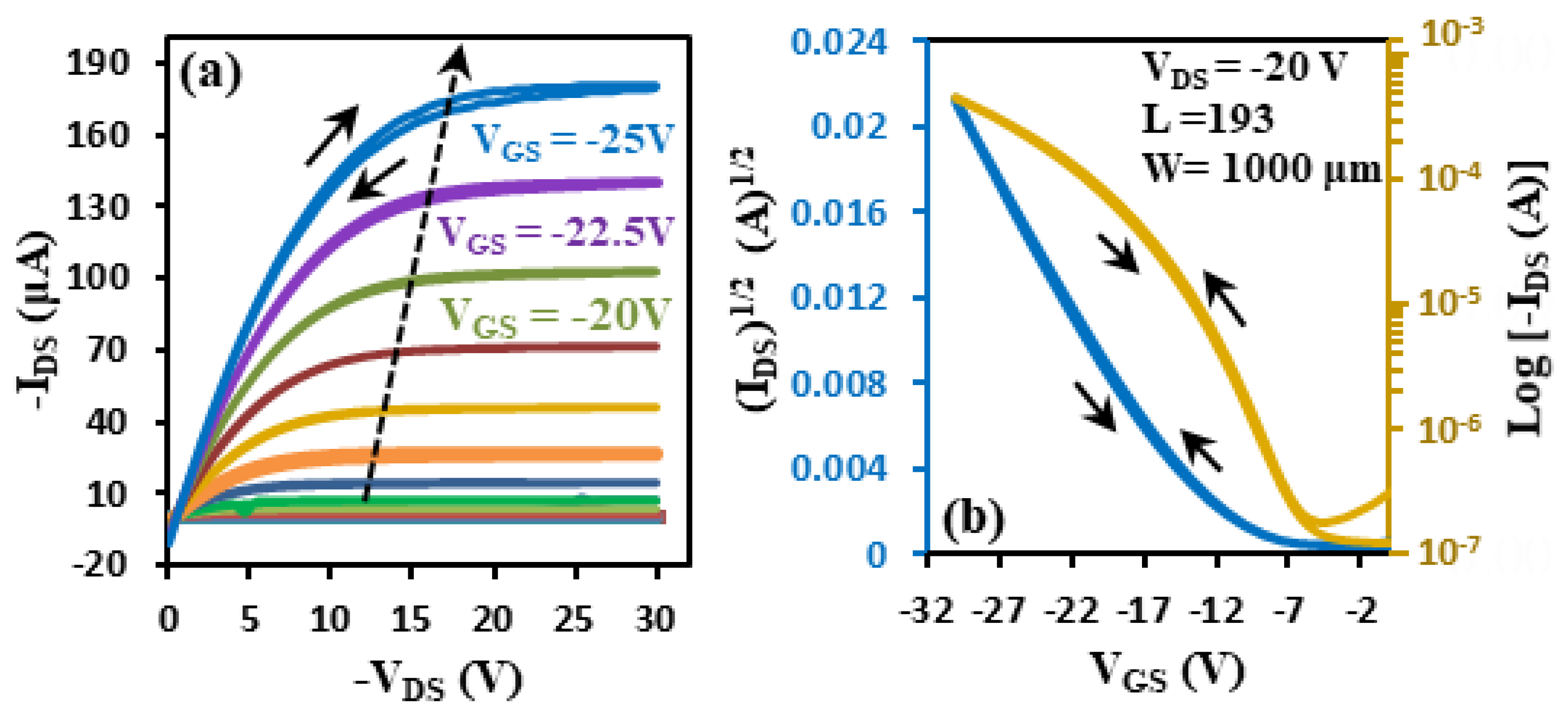
To evaluate the stability of the fabricated OFET devices on flexible substrates, they were tested again in a consecutives months after their first fabrication, where all devices had been vacuum-stored during that time. The output and transfer characteristics of the flexible OFET devices were measured aged devices are shown in Figure 5(a) and Figure 5(b). As can be seen from these figures, the flexible OFET devices exhibit typical p-type OFET behaviour; they are still operating with a high performance, on/off current ratio of 0.26×10⁴ and a high value of μ, which is calculated to be 5.88 cm2/V.s with a Vth of -9 V. Negligible hysteresis was also noticed for the transfer characteristics as well as the output. Moreover, a small leakage current and no significant drain off-set current were observed in these devices.
The significant performance of flexible OFETs is due to the three layers of the insulating material, especially the ZnO and SiO2 layers. The pure ZnO layer with a thickness of 30 nm (the first insulator layer on the Al contact) played an important role in avoiding damage to the gate layer during the bending, exhibiting an enhancement in the OFETs results. The silicon layer between the ZnO and PMMA layers improves the behaviour of the device as a flexible device and increases its effectiveness. As for the last layer of the insulating material, PMMA, its presence directly below the active layer, pentacene, enhances the performance of the transistor device. This enhancement was also achieved and discussed in previous works [27,35].
Based on the results reported in the previous articles [36,37], bending the OFET device causes two potential effects on the properties: the I-V characteristic and the electron mobility. The bending effect depends on whether the bending is downward or upward. In this work, the mobility and current-voltage characteristics of the OFET devices were measured in the downward bending direction, showing slight differences in these measurements. However, bending in the same direction leads to a very small change in the OFETs properties [38].
4. Conclusions
Fabrication and characterization of top-contact organic field effect transistors (OFETs) on glass and flexible PET substrates based on pentacene with the dielectric layers of nano-crystalline ZnO, SiO2, and PMMA have been investigated in this study. High-performance flexible OFETs with high mobility of about 6.92 cm2/V.s, we have successfully demonstrated. This mobility data is the best reported data among flexible OFETs in the literature. Good stability and a long lifetime have been observed in this work. The harmony of the three layers of the insulating material, ZnO (30 nm), SiO2 (50 nm), and PMMA (70 nm), was investigated to enhance the good properties of the OFET device’s work on flexible substrates. There is negligible hysteresis in the output and transfer characteristics, and the stability of OFETs performance is evaluated after one year, where the behaviour of the transfer characteristics exhibited a slight change. This combination makes these devices interesting for high-performance OFET devices for applications on flexible substrates.
References
- Alex, C.; Jia, L.; Zhenan, B. Pursuing prosthetic electronic skin. Nat. Mater 2016, 15, 937–50. [Google Scholar]
- Takao, S.; Zhenan, B.; George, G. M. The rise of plastic bioelectronics. Nature 2016, 540, 379–385. [Google Scholar] [CrossRef]
- Haifeng, L.; Shenghua, L.; Zijian, Z.; Feng, Y. Organic Flexible Electronics. Small Method 2018, 2, 1800070. [Google Scholar]
- Mohamed, S.; Ahmed, H.; Zhenxing, W.; Mehrdad, S.; Daniel, N.; Renato, N. Graphene integrated circuits: new prospects towards receiver realization. Nanoscale 2018, 10, 93–99. [Google Scholar]
- Skotheim, T. A. pi-electron models of conjugated polymers: vibrational and nonlinear optical spectra, in Handbook of conducting polymers: CRC press Marcel Dekker, New York, 1997, 27.
- Samual, E. R.; Suchol, S.; Adam, D. P.; Danil, R.; Darren, J. L. Mechanical Properties of Organic Semiconductors for Stretchable, Highly Flexible, and Mechanically Robust Electronics. Chem. Rev 2017, 117, 6467–6499. [Google Scholar]
- Kenjiro, F.; Takao, S. Recent Progress in the Development of Printed Thin-Film Transistors and Circuits with High-Resolution Printing Technology. Adv. Mater 2017, 29, 1602736. [Google Scholar]
- Ikuo, T.; Shosuke, Y.; Kazumi, H.; Kenji, M.; Yoshiharu, K.; Kohei, O. Biodegradation of PET: current status and application aspects. ACS Catalysis 2019, 9, 4089–4105. [Google Scholar]
- Fu, Y.; Yuting, H.; Yaowen, L.; Yongfang, L. Large-area flexible organic solar cells. npj Flexible Electronics 2021, 5, 1. [Google Scholar] [CrossRef]
- Ja, H. K.; Seongjin, J.; Hyung, J. S.; Donghee, S.; Jaemin, K.; Dong, C. K.; Suji, C.; Jong-In, H.; Dae-Hyeong, K. Wearable Electrocardiogram Monitor Using Carbon Nanotube Electronics and Color-Tunable Organic Light-Emitting Diodes. ACS Nano 2017, 11, 10032–10041. [Google Scholar]
- Su, M.; Yawei, Q.; Ge, M.; Menglu, C.; Xi, T. Multi-Color Light-Emitting Diodes Coatings. Coatings 2023, 13, 182. [Google Scholar]
- Wei, G.; Hiroki, O.; Daisuke, K.; Kuniharu, T.; Ali, J. Flexible electronics toward wearable sensing. Accounts of chemical research 2019, 52, 523–533. [Google Scholar]
- Dayanand, K.; Umesh, C.; Lew, W. S. Tseung-Yuen, T. ZrN-Based Flexible Resistive Switching Memory. IEEE EDL 2020, 41, 705. [Google Scholar]
- Dan, X.; Hongjia, S.; Xiangli, Z.; Jinbin, W.; Nie, Z.; Hongxia, G.; Peitian, C. Flexible resistive switching device based on the TiO2 nanorod arrays for non-volatile memory application. J. Alloys and Compounds 2020, 822, 153552. [Google Scholar]
- Tsukuru, M.; Tomohito, S.; Michio, A.; Tsuyoshi, M. An organic FET with an aluminum oxide extended gate for pH sensing. Sensors and Materials 2019, 31, 99. [Google Scholar] [CrossRef]
- Haider, S. A. Flexible Field effect transistor construction techniques. AL-Qadisiyah J. Eng. Sci. 2021, 14, 112–116. [Google Scholar]
- William, M. Engineered films for display technologies. J. Mater. Chem. 2004, 14, 4–10. [Google Scholar]
- Cristine, B.; Xavier, D.; Etienne, S. Characterization of poly (ethylene terephthalate) used in commercial bottled water. IOP Conference Series Materials Science and Engineering, September 2009.
- Mohammad, G. F.; Kamarulazizi, I.; Mohammed, K. M. PET as a plastic substrate for the flexible optoelectronic applications. Optoelectron. Adv. Mater. 2011, 5, 879–882. [Google Scholar]
- Jae-Min, K.; Taewook, N.; Lim, S. J.; Y. G., Seol; Nae-Eung, L.; Bo, S. K.; Hyungjun, K. Atomic layer deposition ZnO: N flexible thin film transistors and the effects of bending on device properties. Appl. Phys. Lett. 2011, 98, 142113. [Google Scholar]
- Mingdong, Y.; Yuxiu, G.; Jialin, G.; Tao, Y.; Yuhua, C.; Quli, F.; Linghai, X.; Wei, H. The mechanical bending effect and mechanism of high performance and low-voltage flexible organic thin-film transistors with a cross-linked PVP dielectric layer. J. Mater. Chem. C. 2014, 2, 2998. [Google Scholar]
- Lee, K. H.; Lee, K.; Oh, M.; Choi, J.; Im, S.; Jang, S.; Kim, K. Flexible high mobility pentacene transistor with high-k/low-k double polymer dielectric layer operating at −5 V. Org. Electron. 2009, 10, 194. [Google Scholar] [CrossRef]
- Mark, E. R.; Nuria, Q.; Stefan, C. B.; Mannsfeld; Zhenan, B. Cross-Linked Polymer Gate Dielectric Films for Low-Voltage Organic Transistors. Chem. Mater. 2009, 21, 2292. [Google Scholar]
- Se, H. K.; Sang, Y. Y.; Kwonwoo, S.; Hayoung, J.; Jong, W.L.; Ki, P. H.; Chan, E. P. Low-operating-voltage pentacene field-effect transistor with a high-dielectric-constant polymeric gate dielectric. Appl. Phys. Lett. 2006, 89, 183516. [Google Scholar]
- Mingdong, Y.; Jialin, G.; Wen, L.; Linghai, X.; Quli, F.; Wei, H. High-mobility flexible pentacene-based organic field-effect transistors with PMMA/PVP double gate insulator layers and the investigation on their mechanical flexibility and thermal stability. RSC Adv. 2015, 5, 95273. [Google Scholar]
- Yonghwa, B.; Sooman, L.; Eun, J. Y.; Lae, H. K.; Haekyoung, K.; Seung, W. L.; Se, H. K. Fluorinated Polyimide Gate Dielectrics for the Advancing the Electrical Stability of Organic Field-Effect Transistors. ACS Appl. Mater. 2014, 6, 5209. [Google Scholar]
- Sundes, J. F.; Hassan, A.; Mohammed, M. Bias stress effect on high mobility-hysteresis free pentacene-based organic thin film transistors. Synthetic Metals 2014, 191, 53–58. [Google Scholar]
- Constance, R. Ambipolar and Light-emitting Organic Field-Effect Transistors. Cuvillier Verlag 2005, 167. [Google Scholar]
- Takehiko M. Molecular materials for organic field-effect transistor. in Molecular Materials, 1st Edition, Sanjay, M.; B. L. V. Prasad, Jordi, F.; Boca Raton, 2017, p. 30.
- Bonfiglio, A.; Mameli, F.; Sanna, O. A completely flexible organic transistor obtained by a one-mask photolithographic process. Appl. Phys. Lett. 2023, 82, 3550. [Google Scholar] [CrossRef]
- Tsuyoshi, S.; Ute, Z.; Hagen, K.; Takao, S. Flexible organic transistors and circuits with extreme bending stability. Nat. Mater. 2010, 9, 1015. [Google Scholar] [CrossRef]
- Piero, C.; Andrea, P.; Annalisa, B. Fully deformable organic thin-film transistors with moderate operation voltage. IEEE Trans. Electron Devices 2011, 58, 3416. [Google Scholar] [CrossRef]
- Martin, K.; Tsuyoshi, S.; Jonathan, R.; Tomoyuki, Y.; Kazunori, K.; Takeyoshi, T.; Michael, D.; Reinhard, S.; Ingrid, G.; Simona, B.; Siegfried, B.; Takao, S. An ultra-lightweight design for imperceptible plastic electronics. Natural 2013, 499, 458. [Google Scholar]
- Liangkun, L.; Dazhi, W.; Changchang, P.; Yanyan, C.; Yikang, L.; Pengfei, X.; Xiangji, C.; Chang, L.; Shiwen, L.; Liujia, S.; Yan, C.; Zhiyuan, Z.; Yunlong, G.; Junsheng, L.; Yunqi, L. High-performance flexible organic field effect transistors with print-based nanowires. Nature: Microsystems & Nanoengineering 2023, 9, 80. [Google Scholar]
- Sundes, F.; Mohammed, M. Fabrication and characterization of nonvolatile organic thin film memory transistors operating at low programming voltages. Europe. Phys. J. App. Phys. 2012, 60, 10201. [Google Scholar]
- Jae-Min, K.; Taewook, N.; Lim, S. J.; Seol, Y. G.; Lee, N.-E.; Doyoung, K.; Hyungjun, K. Atomic layer deposition ZnO: N flexible thin film transistors and the effects of bending on device properties. Appl. Phys. Lett. 2011, 98, 142113. [Google Scholar]
- Federico, F.; Luca, L.; Angelo, T. Bending device and anticlastic surface measurement of solids under large deformations and displacements. MRC 2019, 97, 52. [Google Scholar]
- Jun, Y.; Peipei, H.; Jin, L.; Lingyan, W.; Melissa, F. C.; Chuan-Jian, Z. Molecularly mediated thin film assembly of nanoparticles on flexible devices: electrical conductivity versus device strains in different gas/vapor environment. ACS Nano 2011, 5, 6516. [Google Scholar] [CrossRef] [PubMed]
Figure 1.
Schematic diagrams of the pentacene-based OTFTs on glass and flexible substrate.

Figure 2.
AFM images of the pentacene thin film grown on PMMA/SiO2/ZnO triple gate insulator layers with scan area size (a) 7.0 µm and (b) 3.4 µm.
Figure 2.
AFM images of the pentacene thin film grown on PMMA/SiO2/ZnO triple gate insulator layers with scan area size (a) 7.0 µm and (b) 3.4 µm.
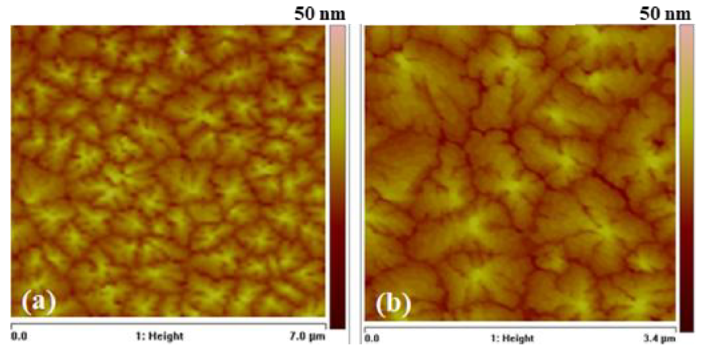
Figure 3.
The (a) output and (b) transfer characteristics of a pentacene-based OTFT on glass substrate.
Figure 3.
The (a) output and (b) transfer characteristics of a pentacene-based OTFT on glass substrate.
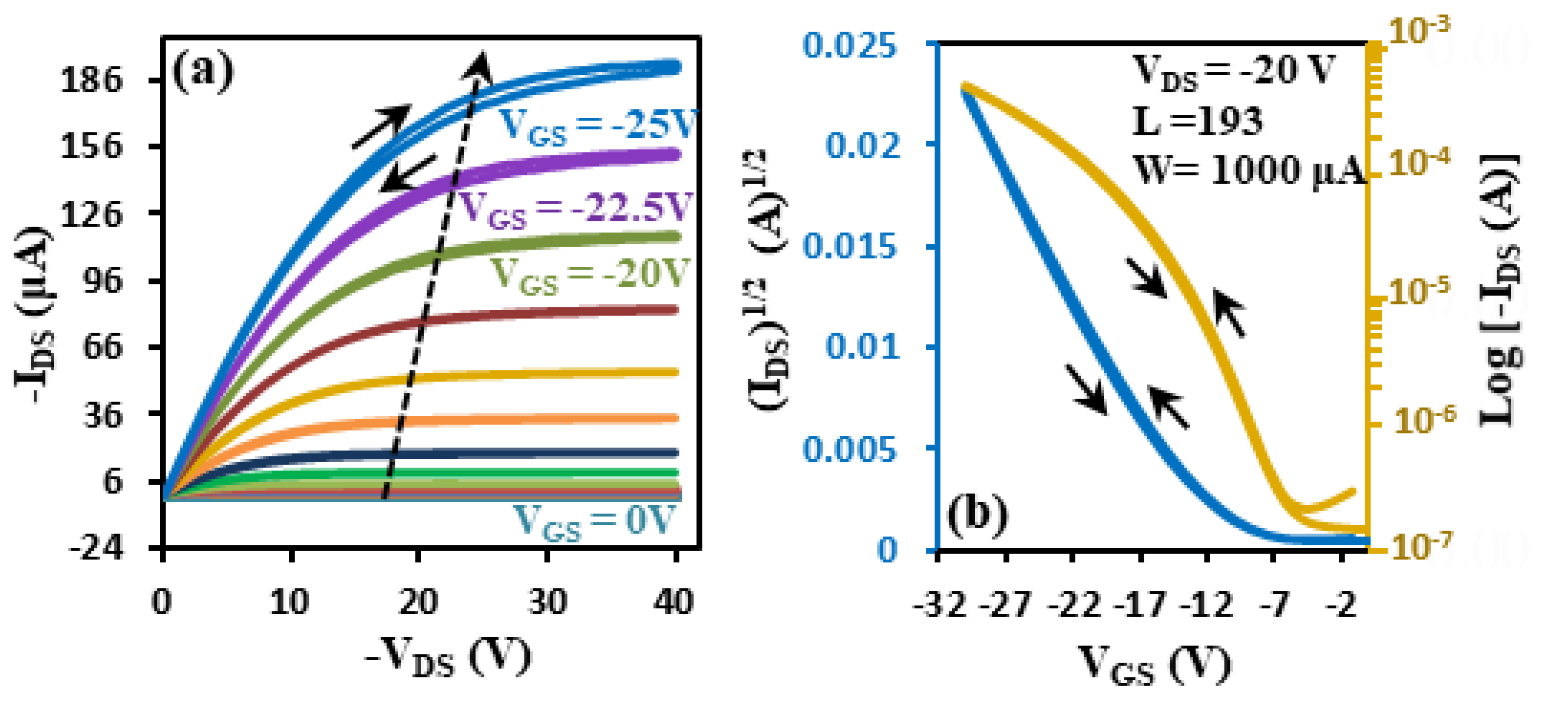
Figure 4.
The (a) output and (b) transfer characteristics of a pentacene-based OTFT on flexible PET substrate before bending. (c) output and (d) transfer after bending.
Figure 4.
The (a) output and (b) transfer characteristics of a pentacene-based OTFT on flexible PET substrate before bending. (c) output and (d) transfer after bending.
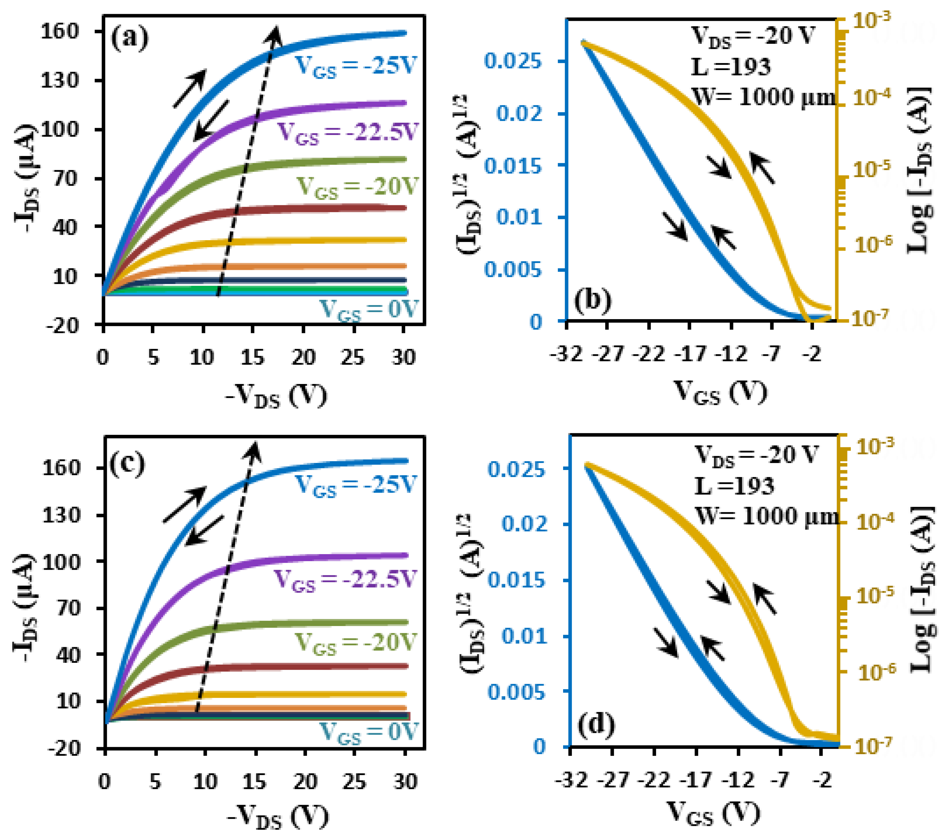
Figure 5.
The (a) output and (b) transfer characteristics of a pentacene-based OTFT on flexible PET substrate aged device.
Figure 5.
The (a) output and (b) transfer characteristics of a pentacene-based OTFT on flexible PET substrate aged device.
Disclaimer/Publisher’s Note: The statements, opinions and data contained in all publications are solely those of the individual author(s) and contributor(s) and not of MDPI and/or the editor(s). MDPI and/or the editor(s) disclaim responsibility for any injury to people or property resulting from any ideas, methods, instructions or products referred to in the content. |
© 2025 by the authors. Licensee MDPI, Basel, Switzerland. This article is an open access article distributed under the terms and conditions of the Creative Commons Attribution (CC BY) license (http://creativecommons.org/licenses/by/4.0/).
Copyright: This open access article is published under a Creative Commons CC BY 4.0 license, which permit the free download, distribution, and reuse, provided that the author and preprint are cited in any reuse.


