Submitted:
02 August 2025
Posted:
04 August 2025
You are already at the latest version
Abstract
Epitaxial growth of InN film by metalorganic chemical vapor deposition (MOCVD) is investigated with adding an InGaN bedding layer. The structure and optical properties of the InN film are in-vestigated by transmission electron microscopy (TEM) and photoluminescence (PL). From the se-lective area electron diffraction pattern in the TEM, the InN is found to be almost strain free. At low temperature of 8 K, strong PL of the InN film indicate that the energy band gap of the InN is about 0.75 eV. The anomalous persistent PL decay behavior under continuous-wave excitation has been observed and discussed as the surface recombination and strong surface/interface effect of the InN film. These results indicate that suppressing and eliminating surface/interface states is one of the key factors in enhancing the performance of the InGaN-based long-wavelength optoe-lectronic devices, which is significant for the development of efficient long-wavelength (red and beyond) InGaN or InN devices.
Keywords:
InN
; photoluminescence
; surface recombination
1. Introduction
In the III-V nitride family, InN is quite special and different from GaN and AlN which have been systematically studied and widely used in visible-ultraviolet optoelectronic devices along with their alloys. In contrast, material property studies on InN present significant challenges. For instance, the determination of the band gap (Eg) has ever undergone a tortuous research history. This is mainly due to the extremely high equilibrium vapor pressure of nitrogen on InN, which is several orders of magnitude higher than that of AlN and GaN, making it difficult to grow high-quality InN crystals [1,2]. Early studies used sputtering techniques [3,4,5,6,7,8] and metal organic chemical vapor deposition (MOCVD) [9] to grow polycrystalline or nanocrystalline InN materials, which had poor crystallinity. The Eg was estimated to be around 1.8 to 2.0 eV at room temperature through absorption spectroscopy without luminescence results. Subsequently, a bandgap value of 1.9 eV was widely accepted for a long time and often used as the extrapolated endpoint value for the bandgap in InGaN alloys [10]. In 2001, Yodo et al. [11] first observed that InN grown on a Si substrate exhibited photoluminescence (PL) at the band edge near 1.814 eV, suggesting that these emissions were due to donor-acceptor pairs and donor-bound exciton emissions of wurtzite InN grains, but unfortunately, this was soon proven to be incorrect.
At the end of 2001, Davydov et al. grew single-crystal InN epitaxial layers on sapphire substrates using MOCVD [12,13]. They compared the optical absorption and PL of InN, and PL measurement showed a strong PL emission near the absorption edge between 0.75 eV and 0.9 eV, which corresponds to the Eg of InN. This is the first report of the correct Eg. A few months after Davydov’s finding was published, in early 2002, Wu et al. grew InN single-crystal epitaxial films by using molecular beam epitaxy (MBE), and then they repeated the PL measurements around 0.75 eV [14]. No surprise, they also obtained the result of InN’s Eg around 0.75 eV. This convoluted history reflects the complexity of InN material properties, but the challenges in studying the characteristics of InN materials are clearly not limited to this one.
In recent years, the research on InGaN-based red to infrared long-wavelength optical devices has gradually become a research hotspot, such as in the studies of photodetectors, solar cells, and light-emitting devices [15,16,17,18]. Although significant progress has been made in high-quality InN epitaxy, high-quality InN material still faces tremendous challenges due to the inherent properties of InN. First is the huge difference in equilibrium vapor pressure between N and In, which often leads to the formation of liquid In droplets on the epitaxial surface [19]. Secondly, the huge lattice mismatch between the InN film and the substrate material leads to significant stress and a high defect density. Even though growing InN on a GaN substrate relatively reduces the mismatch, there is still about an 11% lattice mismatch, which generates substantial stress. During the growth of InN, the film stress has a significant effect on the surface state of the InN film. These issues require adjustments to the epitaxial conditions and structures to avoid indium segregation and reduce the stress in the epitaxial InN film.
As the key points of high-quality epitaxy of InN are gradually discovered, corresponding epitaxy technologies are developed, leading to a gradual improvement in material quality. A technique for the growth of high-quality InN utilizing an InGaN bedding layer was developed by our group and published in 2023 [20]. By adopting a proper In composition (23% in that work), low-stress high-quality InN films were grown with strong PL around 0.74 eV at room temperature. Subsequently, in 2024, Shetty et al. continued to use this InGaN bedding layer structure for growing high-quality InN films up to 0.5 μm, achieved a mobility exceeding 2000 cm2/V·s at a low temperature of 80 K [21].
In addition to the difficulties in crystal growth, the narrow bandgap of InN is usually accompanied by strong surface states, resulting in a more complex luminescence mechanism. In fact, most InN samples are degenerate n-type materials with an electron concentration of about 1×1018 cm−3 or even higher [22]. Therefore, the luminescence characteristics of InN may deviate from classical semiconductor radiative recombination laws. On the other hand, the performance of long-wavelength optoelectronic devices based on InGaN becomes increasingly correlated with the characteristics of InN itself as the wavelength increases. For example, even with the same crystal quality, the luminous efficiency of green LEDs or LDs is still lower than that of blue devices, and the efficiency of red devices is even lower. Surface states and surface recombination effects are very significant in narrow bandgap semiconductor materials [23,24], but current research on the recombination mechanisms of InN is far from sufficient, and surface recombination in InN remains a largely unexplored area of research. This also partly leads to the fact that despite the extensive work done by many research teams in photovoltaics and red LEDs, the power conversion efficiency (PCE) of current InGaN-based solar cells still lags far behind the theoretical values (>20%) [25], and the luminous efficiency of red LEDs still does not exceed 10% [15,26].
This work successfully grew high-quality InN single crystal films on sapphire substrates with the InGaN bedding layer by using the MOCVD method. The structure of InN was characterized by transmission electron microscopy (TEM), and its unique luminescent properties under strong surface effects were investigated. The research results will contribute to the development of high-efficiency long-wavelength InGaN-based optoelectronic devices.
2. Materials and Methods
The schematic diagram of the sample structure for the experimental study is shown in Figure 1. The overall structure includes a 25-nm GaN buffer layer, a 1.5-μm undoped GaN epitaxial layer, as well as InGaN and InN layers, with the InN layer being approximately 150 nm thick. The samples are grown on c-plane sapphire substrates using the MOCVD method, and details of the growth can be referenced from Ref. 20.
Structural characterization of InN, including X-ray diffraction (XRD) and scanning electron microscopy (SEM) analysis, is detailed in Ref. 20. Furthermore, we studied the optical properties of InN through temperature-dependent PL here. The measurement temperature ranges from 8K to 300K. To pump the InN and collect emissions, we use a confocal Renishaw invia-reflex μ-PL setup with an 808-nm continuous-wave (cw) laser, the excitation power density is adjustable from 2.5 to 64 W/cm2. The detector consists of a spectrometer and a Peltier-cooled charge coupled device (CCD).
3. Results
The cross-sectional TEM image of the grown InN sample is shown in Figure 2. From the figure, the dislocation distribution within each layer can be observed. Since the thickness of the underlying GaN layer is only 1.5 μm, so it is normal for the dislocation density in the epitaxial layer to be relatively high. In Figure 2(a), V-shaped pits on the surface of the InN layer can be seen, noting that not all dislocations lead to V-shaped pits. It is commonly believed that V-shaped pits result from stress release, where dislocations serve as the origin for this stress release. However, when some dislocations do not lead to V-shaped pits, it suggests that the stress within the film is not significant. This assumption can be confirmed in Figure 2(b).
Figure 2(b) shows the selected area electron diffraction pattern of the sample which includes the InN layer and part of the underlying GaN layer, with diffraction spots indexed. The two sets of diffraction patterns from GaN and InN can be clearly seen. The absence of tailing distortion of the spots proves that the lattice distortion is small, and the calculated InN lattice constants (compared to theoretical values) are 0.361 (0.355), 0.563 (0.569) nm, respectively. It is evident that these values are very close to the theoretical values, indicating that the epitaxial InN film is almost stress-free. The main reason is that the InGaN bedding layer below not only reduces the lattice mismatch but also helps to relieve stress.
The temperature-dependent PL spectrum of InN is shown in Figure 3(a), with the excitation power at 45 W/cm2. The PL spectrum of InN exhibits a perfect edge luminescence peak, with the peak position red-shifting from 1645 nm at 8 K to 1670 nm at room temperature. The spectral shape of PL curves is steeper on the long-wavelength side (low energy side) and flatter on the short-wavelength side (high energy side), showing typical edge luminescence characteristics. The high-energy side tailing is caused by the continuous filling of the energy band by the high concentration of non-equilibrium carriers, which is consistent with previous reports. The change in the PL intensity with temperature is shown in Figure 3(b). It is generally believed that defects, impurities, and other non-radiative recombination centers are thermally activated with increasing temperature, and the density of non-radiative recombination centers increases exponentially with temperature, leading to the exponential decrease of edge luminescence intensity with temperature, as shown by the red dashed line in Figure 3(b). However, within the temperature range of 80 to 180K, the PL intensity of InN deviates upward from the conventional exponential decay trend. This indicates that in addition to the conventional temperature-related non-radiative recombination centers, there exists another recombination mechanism in InN that is less temperature-dependent, resulting in the maintenance of the PL intensity within the 80 to 120K. This reflects that the recombination mechanisms in the narrow bandgap InN are more complex than those in the wide bandgap GaN.
Further PL measurements of the sample revealed more strange phenomena. During continuous repetitive PL measurements, it is found that the PL spectrum gradually decreased, as shown in Figure 4. This decrease was especially pronounced at lower temperatures. Figure 4(a) shows results at 8K, with measurements taken every 20 seconds, totaling 8 measurements over 160 seconds. It can be observed that the PL spectrum decreases and shows redshift, but ultimately it seems to stabilize. Initially, it is suspected that the excitation power density was too high, causing surface damage to the sample. However, the observation of stable spectra contradicts the idea of damage being the cause. Further measurements revealed that this PL decrease could be completely restored after stopping laser irradiation for about 15 minutes. This proves that laser irradiation damage is not the reason for the decrease and redshift in the PL spectra, it seems more like it comes from the capture and release of charge carriers.
At higher temperatures, a similar phenomenon is observed. As shown in Figure 4(b), measurements were taken every 30 seconds at 52K, resulting in a total of 8 measurements over 240 seconds. It can be seen more clearly that the trend of the spectrum stabilizing is more pronounced at higher temperature. It should be noted that in all curves 1-8 in Figures 4(a)/(b), all measurement conditions remained unchanged, therefore, the decrease in PL solely originates from the internal luminescent mechanism of InN itself. In terms of the basic PL process, after laser excitation, the distribution of excess carriers will play an important role in the final luminescent behavior. According to Figure 4, it can be concluded that there exists a certain carrier leakage mechanism in the InN sample, which is consistent with our previous observations [20]. This carrier leakage is not caused by localized states with saturation characteristics, but is related to external excitation. So. It can lead to a gradual decrease in the effective carrier density over time, until leakage reaches a steady-state balance with excitation and radiative recombination under constant external excitation.
InN is a narrow bandgap semiconductor, and the effects of band bending caused by surface states are more pronounced compared to wide bandgap semiconductors such as GaN. This has been widely recognized in traditional narrow bandgap semiconductors like InAs and InP [23,24]. For example, in InAs devices with properly passivated surfaces, the elimination of surface state effects can enhance the photoluminescence intensity by ten times [24]. This demonstrates the significant impact of surface/interface states on narrow bandgap materials. Although nitride semiconductors are generally considered wide bandgap semiconductors, the ~0.7 eV bandgap of InN indeed falls into the narrow bandgap category. Above PL measurements indicate that the surface/interface effects, which are not evident in GaN and AlN, need to be carefully considered in InN.
In order to clearly study the variation of InN PL with time, we designed a new PL measurement method. First, we added a shutter to block the laser in the optical path, fixed the detection center wavelength on the spectrometer, and adjusted the width of the slit to cover a detectable wavelength range of approximately 200 nm. This ensures that we can record the complete luminescence peak intensity. Then this optical path setting was fixed for all measurements. Secondly, during the measurements, we open the shutter at the appropriate time to allow the laser to pass through, exciting the sample. We continuously record the change in PL intensity over time. In this way, we can record the change in PL intensity over time of the sample from the moment it is excited under continuous excitation.
The measurement results are shown in Figure 5, with the vertical axis of PL intensity using a logarithmic scale. Figure 5 shows that at various temperatures from 20 K to 200 K, the PL intensity exhibits an exponential decline, ultimately approaching a “stable intensity” state. As the temperature increases, the time to reach the stable intensity is shorter. The final stable intensity also appears to be similar at those higher temperatures, and its relationship with temperature is not obvious. At the higher temperatures than 200 K, the change in PL intensity over time becomes less noticeable, so it is not displayed.
In Figure 5, although the initial luminescence intensities are different, the decay curves are nearly ‘parallel’ at most temperatures, showing that this decline is not strongly related to temperature or the equivalent thermal activation process. This feature is difficult to explain by using conventional PL models. The PL special characteristics of the InN have been reflected in Figure 3(b), where the PL intensity shows a weak correlation with temperature in the medium temperature range.
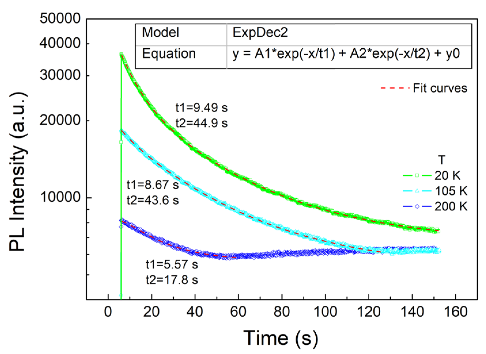
To more clearly display the decay features, we fitted the curves at three typical temperatures (20 K, 105 K, 200 K), as shown in Figure 6, where the red dashed line represents the fitting results. The fitting used a double exponential model, with the formula shown in the figure.
As shown in Figure 6, the double exponential fitting can accurately fit the measurement curves, with each curve displaying two decay time constants t1 and t2, indicating the presence of both fast and slow processes. Similarly, the radiation process exhibits both fast and slow processes, which are quite common in the InGaN system and have been reported in many experiments [27,28,29]. At 20 K, t1 and t2 are 9.49 s/44.9 s respectively, at 105 K they are 8.67 s/43.6 s, and at 200 K they are 5.57 s/17.8 s. At the lower temperatures of 20 K and 105 K, t1 and t2 do not differ much, only slightly shortening with increasing temperature. However, at 200 K, t1 and t2 shorten significantly, indicating a substantial change in the internal recombination processes.
In the typical PL theory, the first step is that if the sample is continuously excited by a stable cw laser, then the ‘supply’ of excess carriers should be constant (there is a prerequisite here: the light absorption by valence band electrons is dominant, while the absorption of others is small and can be ignored). Then in the second step, the excess carriers recombine through several recombination channels, of which the non-recombination channels are usually closely related to temperature. Generally, in this case, the intensity of PL remains unchanged over time and is highly correlated with temperature changes. The equation for the excess carriers after excitation should be as follows,
Here G represents the carrier generation rate and n represents the excess carrier concentration. It is widely accepted that there are mainly three carrier-recombination mechanisms in normal semiconductors, that are Shockley-Read-Hall (SRH, An) nonradiative recombination, bimolecular radiative recombination (Bn2) and Auger nonradiative recombination (Cn3). A, B and C are the recombination coefficients of their respective recombination mechanisms. K are the recombination coefficient of unknown recombination mechanism. Typically, the Auger coefficient C is very small, and Auger recombination can be ignored at low carrier concentrations. The K process is only considered when there are obvious signs in the experiment, as in our previous study on the droop effect [30].
However, the actual material properties can be more complex, and if the material characteristics lead to significant alternative transition in the light absorption in the first step, then even if the sample is continuously excited by a stable cw laser, the ‘supply’ of excess carriers, or the G in Eq. (1), will change, and the behavior of the emitted light intensity will consequently vary.
As a narrow bandgap semiconductor, InN exhibits more pronounced effects caused by surface/interface states, which is a common pattern seen in narrow bandgap semiconductors like InAs and InP etc. The effect of the interface states is resulted in a constant Surface Recombination Velocity (S) such as made in the simple theory [31,32]. It has been assumed that the surface recombination center is located at midgap and capture cross sections for electrons and holes are equal. However, the actual situation is more complicated, and the surface recombination velocity may not be constant, for example, the energy bands may curve at the surface. In fact, the S of silicon has for long been known to be a strong function of the surface potential [33]. Girisch et al. modeled the Si/SiO2 interface with an extended SRH-algorithm, that also accounts for band-bending effects due to oxide charges and charges in the interface states [34].
Further detailed analysis has been done by Mui et.al. [35,36], which provided a deeper investigation on the effects of surface recombination on carrier distributions. In this paper, they use SRH recombination mechanism to calculate the surface recombination. They found that surface recombination S is proportional to the densities of empty and filled surface traps, respectively, contrary to the usual assumption that S is proportional to the surface trap density. In another word, there will be an “effective density” for the surface recombination. Furthermore, the charged traps will change with trap density and generation rate. Then, for a given injection condition, the luminescence intensity depends critically on the effective density of surface traps.
These complex surface processes happen to occur easily in InN. Some of InN’s unique properties have been studied and discovered, especially the surface band bending that forms surface electron accumulation, as shown in the work of Veal et.al. [37]. Their results indicate the extreme nature of the electron accumulation at the surface of n-type InN, in agreement with findings obtained using a wide range of experimental techniques. The nature of the band structure of InN, with its particularly low Γ-point conduction band minimum, dictates the existence of positively charged donor-type interface states, and huge band bending near the surface, leading to electron accumulation at InN surface/interfaces. According to their calculation, the electron density in the accumulation layer peaks at greater than 2×1020 cm-3 at a depth of ~0.4 nm. Then, such high-density electron accumulated at the surface will certainly fill the surface traps, thereby reducing the effective surface trap density.
According to the special surface state of InN, our PL experiment process should be like this. The initial state of the sample is as described above; the InN grown by MOCVD is inherently n-type, resulting in strong electron accumulation on the surface. At this time, the surface states are filled. Therefore, when the sample is excited by laser, the initial phase of PL measurement shows the highest PL intensity. However, due to the very high concentration of electrons accumulated on the surface, the excitation of these surface electrons by the incident laser cannot be ignored at this time, and with increasing exposure time, more surface electrons absorb photons from the laser, resulting in a decrease in valence band absorption. This decrease is equivalent to G. At the same time, surface-accumulated electrons are continuously excited, leading to a decrease in surface electron concentration, which in turn activates some traps that were originally filled. Therefore, in this case, the continuous irradiation reduces the effective excess carrier generation rate and increases non-radiative surface recombination, ultimately leading to the observed continuous decline in the PL spectrum. Therefore, the degree of PL intensity decline depends on the density of effective traps. After a long period of exposure, the concentration of activated traps increases, and ultimately reaches equilibrium with the supply of excess carriers, which is the final “stable intensity” observed in Figure 5. This process is clearly not very related to temperature.
Of course, temperature still plays an important role in the PL process, and traps activated by high thermal energy should not be filled by the surface electrons. At higher temperatures, thermal energy excites more traps, weakening the effect of surface electron filling. As a result, the degree of decline decreases, while the overall PL intensity is not high, and the PL reaches the “stable state” earlier.
This model can also explain Figure 3(b). The bulge at moderate temperatures is due to the fact that at the temperature from 80 to 150K, the surface states activated at low temperatures are entirely filled by the surface electrons, then the PL intensity remines. It is only after reaching higher temperatures that more deeper states are thermally activated. This model can be compared with the fitted t1/t2 results in Figure 6; at low temperatures, both t1 and t2 are similar, indicating that the concentration of effective surface states is roughly the same. However, at the high temperature, both t1 and t2 becomes much shorter, indicating that the concentration of effective surface states is increased.
Based on the analysis above, it can be seen that the model proposed in this work can explain current phenomena that have been discovered, but further in-depth research is still needed. Due to the special mechanism under the surface/interface modulation of InN, the often-overlooked surface/interface effects are manifested in materials/devices with high InN content. For example, as mentioned earlier, even with the same crystal quality, the luminous efficiency of green LEDs or LDs is still lower than that of blue devices, and the efficiency of red devices is even lower. The findings and proposed model in this paper help to understand these phenomena.
4. Conclusions
In conclusion, high-quality InN single-crystal film with the InGaN bedding layer was grown by MOCVD. The InGaN bedding layer significantly reduced film stress. The effects of surface recombination and strong surface/interface effect of the InN film have been investigated. The nature of the band bending near the surface and the high-density electron accumulation at InN surface/interface modulated the surface recombination, and leading to the continuous decline in the PL spectrum under continuous excitation. The findings and proposed model in this paper help to understand the low efficiency of InGaN-based long-wavelength optoelectronic devices. As a result, suppressing and eliminating surface/interface states is one of the key factors in enhancing the performance of the InGaN-based long-wavelength optoelectronic devices, requiring targeted design at the surface/interface, which awaits further in-depth research.
Author Contributions
Conceptualization, P.C.; formal analysis, P.C.; methodology, P.C., Z.X., D.C., X.X. and B.L; software, P.C.; investigation, P.C.; resources, P.C.; data curation, P.C.; writing—original draft preparation, P.C.; writing—review and editing, P.C.; supervision, Y.S.,R.Z. and Y.Z; project administration, P.C.; funding acquisition, P.C. All authors have read and agreed to the published version of the manuscript.
Funding
This work is supported by National Nature Science Foundation of China, grant number 12074182.
Data Availability Statement
All data, theory detail, simulation detail that support the findings of this study are available from the corresponding authors upon reasonable request.
Conflicts of Interest
The authors declare no conflict of interest.
References
- Ghani, B. A; Hashimoto, A.; and Yamamoto, A. ; Indium nitride (InN): A review on growth, characterization, and properties, Journal of Applied Physics, 2003, 94, 2779.
- Ambacher, O.; Brandt, M.; Dimitrov, R.; et al. , Thermal stability and desorption of Group III nitrides prepared by metal organic chemical vapor deposition, J. Vac. Sci. Technol. B 1996, 14, 3532. [Google Scholar] [CrossRef]
- Osamura, K.; Nakajima, K.; and Murakami, Y. ; Fundamental absorption-edge in GaN, InN and their alloys, Solid State Communication, 1972, 11, 617.
- Tansley, T. L.; and Foley, C. P. ; Optical band-gap of indium nitride, Journal of Applied Physics, 1986, 59, 3241. [CrossRef]
- Westra, K.L.; Lawson, R. W.; and Brett, M. J. ; The effects of oxygen contamination on the properties of reactively sputtered indium nitride films, Journal of Vacuum Science and Technology, 1988, A6, 1730. [CrossRef]
- Ikuta, K.; Inoue, Y.; and Takai, O. ; Optical and electrical properties of InN thin films grown on ZnO/alpha-Al2O3 by RF reactive magnetron sputtering, Thin Solid Films, 1998, 334, 49. [CrossRef]
- Tyagai, V.A.; Evstigneev, A.M.; Krasiko, A.N.; et al. Optical-properties of indium nitride films, Soviet Physics Semiconductor, 1977, 11, 1257.
- Puychevrier, N.; and Menoret, M. ; Synthesis of 3-5 semiconductor nitrides by reactive cathodic sputtering, Thin Solid Films, 1976, 36, 141.
- Guo, Q.; and Yoshida, A. ; Temperature-dependence of band-gap change in InN and AlN, Japan Journal of Applied Physics, Part 1, 1994, 33, 2453. [CrossRef]
- Wetzel, C.; Takeuchi, T.; Yamaguchi, S.; et al. Optical band gap in Ga1-xInxN (O <x <0. 2) on GaN by photoreflection spectroscopy, Applied Physics Letters, 1998, 73, 1994. [Google Scholar] [CrossRef]
- Yodo, T.; Ando, H.; Nosei, D.; et al. Growth and characterization of InN heteroepitaxial layers grown on Si substrates by ECR-Assisted MBE, Physica Status Solidi (b), 2001, 228, 21.
- Davydov, V. Y.; Klochikhin, A. A.; Seisyan, R. P.; et al. Absorption and emission of hexagonal InN. Evidence of narrow fundamental band gap, Physica Status Solidi (b), 2002, 229, R1. [Google Scholar] [CrossRef]
- Davydov, V. Y.; Klochikhin, A. A.; Emtsev, V. V.; et al. Band gap of InN and In-rich InxGa1-xN alloys (0. 36 <x <1), Physica Status Solidi (b), 2002, 230, R4. [Google Scholar]
- Wu, J.; Walukiewicz, W.; Yu, K. M.; et al. Unusual properties of the fundamental band gap of InN, Applied Physics Letters, 2002, 80, 3967. [CrossRef]
- Cheng, A.; Hao, Z.; Sun, C.; et al. , Recent progresses on InGaN red micro-LEDs for display, Progress in Quantum Electronics, 2025, 102, 100575. [CrossRef]
- Li, Z,; et al. , Advancements in InGaN-Based Red Micro-LEDs, IEEE Open Journal on Immersive Displays, 2024, 1, 62–70.
- Afkir, N. B.; Feddi, E.; Dujardin, F.; et al. , Photovoltaic conversion efficiency of InN/InxGa1-xN quantum dot intermediate band solar cells. Physica B: Condensed Matter, 2018, 534, 10. [Google Scholar] [CrossRef]
- Zhao, Y.; Xu, M.; Huang, X. ; Toward high efficiency at high temperatures: Recent progress and prospects on InGaN-Based solar cells, Materials Today Energy, 2023, 31, 101229. [CrossRef]
- Chaly, V. P.; Borisov, B. A.; Demidov, D. M.; et al. , Indium droplet formation during molecular beam epitaxy of InGaN Journal of Crystal Growth, 1999, 206, 147.
- Yin, X.; Chen, P.; Liang, Z.; Zhao, H. ; Epitaxial Growth and Optical Properties of InN film by Metalorganic Chemical Vapor Deposition, Journal of Synthetic Crystals, 2023, 52(5), 791-797.
- Shetty, S.; Kuchuk, A. V.; et al., Improved Quality of InN Thin Films Using a Thin InGaN Compressive Strain Gradient Layer, Crystal Growth Design, 2024, 24, 6115−6123. [CrossRef]
- Veala, T.D.; Pipera, L.F.J.; Schaffb, W.J.; McConvillea, C.F. ; Inversion and accumulation layers at InN surfaces, Journal of Crystal Growth, 2006, 288, 268–272. [CrossRef]
- Choi, C.; et al., Electrical and optical properties of core-shell InAs-InAsyP1-y nanowires, Current Applied Physics, 2017, 17, 1742-1746.
- Jurczak, P.; et al., Ten-Fold Enhancement of InAs Nanowire Photoluminescence Emission with an InP Passivation Layer Nano Letters, 2017, 17, 3629−3633. [CrossRef]
- Zhao, Y.; et al. , Toward high efficiency at high temperatures: Recent progress and prospects on InGaN-Based solar cells, Materials Today Energy, 2023, 31, 101229. [CrossRef]
- Li, P.; Hongjian Li, H.; Yao, Y.; Significant Quantum Efficiency Enhancement of InGaN Red Micro-Light-Emitting Diodes with a Peak External Quantum Efficiency of up to 6%, ACS Photonics 2023, 10, 1899−1905. [CrossRef]
- Tao Lin, T.; et al., Investigation of photoluminescence dynamics in InGaN/GaN multiple quantum wells, Materials Letters, 2016, 173, 170–173. [CrossRef]
- Feng, S.W.; et al. , Multiple-component Photoluminescence decay caused by carrier transport in InGa/GaN multiple quantum wells with indium aggregation structures, Applied Physics Letters, 2002, 80, 4375–4377. [CrossRef]
- Sun, G.; et al. , Investigation of fast and slow decays in InGaN/GaN quantum wells, Applied Physics Letters, 2011, 99, 081104. [CrossRef]
- Jiang, F.; et al. , The Study on the Droop Effect in the InGaN/AlGaInN MQWs, IEEE Photonics Journal, 2018, 10(2), 8200609. [CrossRef]
- Goodman, A. M. ; Method for Measurement of Short Minority Carrier Diffusion Lengths in Semiconductors, Journal of Applied Physics, 1961, 32, 2550. [CrossRef]
- Saritas, M.; and McKell, H. D. ; Diffusion Length Studies in Silicon by The Surface Photovoltage Method, Solid State Electron. 1988, 31, 835. [CrossRef]
- Buck, T. M. ; McKim, F, S. ; Effects of Certain Chemical Treatments and Ambient Atmospheres on Surface Properties of Silicon, Journal of The Electrochemical Society, 1958, 105, 709. [Google Scholar] [CrossRef]
- Girisch, R. B. M.; Mertens, R. P.; Keersmaecker, R. F. ; Determination of Si-Sio2 Interface Recombination Parameters Using a Gate-Controlled Point-Junction Diode Under Illumination, IEEE Transactions on Electron Devices, 1988, 35 (2), 203-222. [CrossRef]
- Zhang, X.; and Song, J. ; The effect of surface recombination on surface photovoltage in semiconductors, Journal of Applied Physics, 1991, 70, 4632–4633. [CrossRef]
- Mui, D.; Coldren, L. A. ; Effects of surface recombination on carrier distributions and device characteristics, Journal of Applied Physics, 1995, 78, 3208–3215. [CrossRef]
- Veala, T.D.; Pipera, L.F.J.; Schaffb, W.J.; McConvillea, C.F. ; Inversion and accumulation layers at InN surfaces, Journal of Crystal Growth, 2006, 288, 268–272. [CrossRef]
Figure 1.
InN epitaxial structure with the InGaN bedding layer.
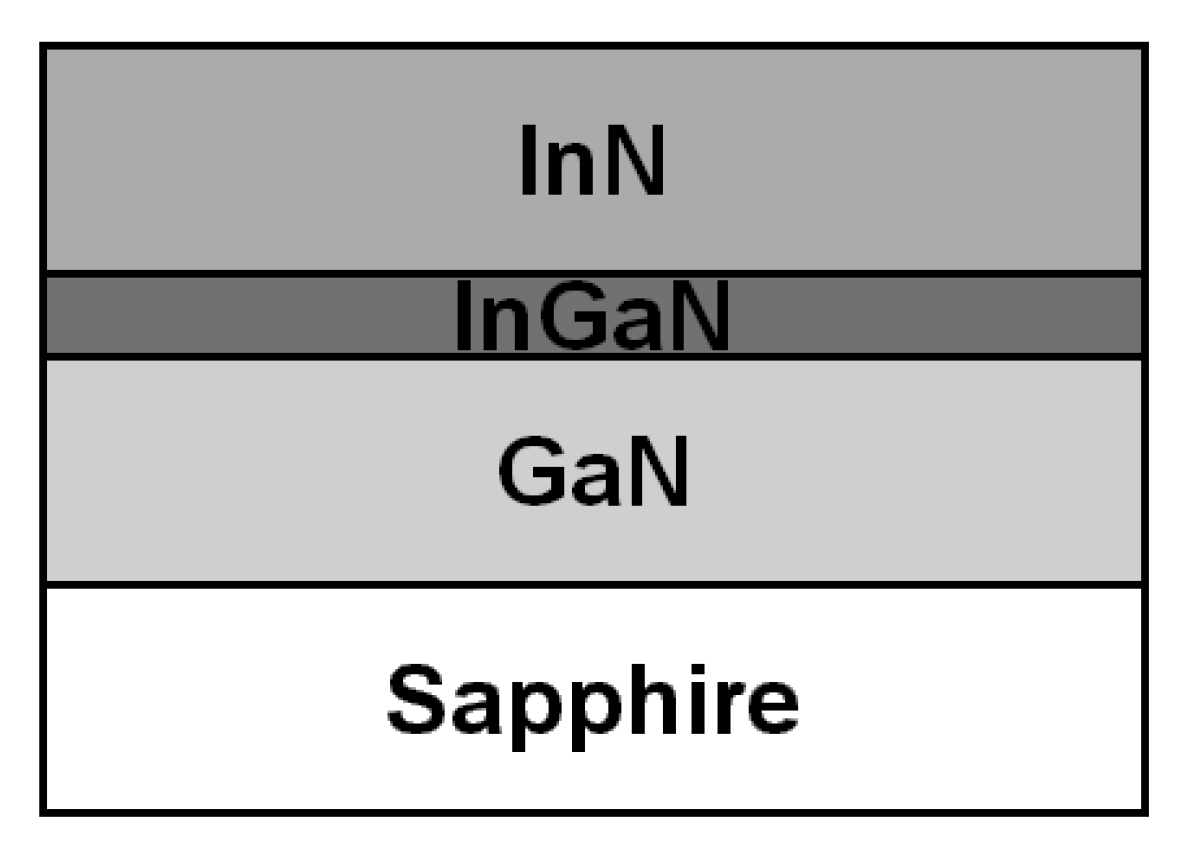
Figure 2.
TEM image of InN film grown to about 150 nm (a), and the selected area diffraction patterns (b).
Figure 2.
TEM image of InN film grown to about 150 nm (a), and the selected area diffraction patterns (b).

Figure 3.
PL spectra of InN film at temperatures from 8 K to 300 K (a), and the relationship between peak intensity and excitation power density (b).
Figure 3.
PL spectra of InN film at temperatures from 8 K to 300 K (a), and the relationship between peak intensity and excitation power density (b).

Figure 4.
PL results at 8K, totaling 8 measurements over 160 seconds (a), PL results at 52K, totaling 8 measurements over 240 seconds (b).
Figure 4.
PL results at 8K, totaling 8 measurements over 160 seconds (a), PL results at 52K, totaling 8 measurements over 240 seconds (b).
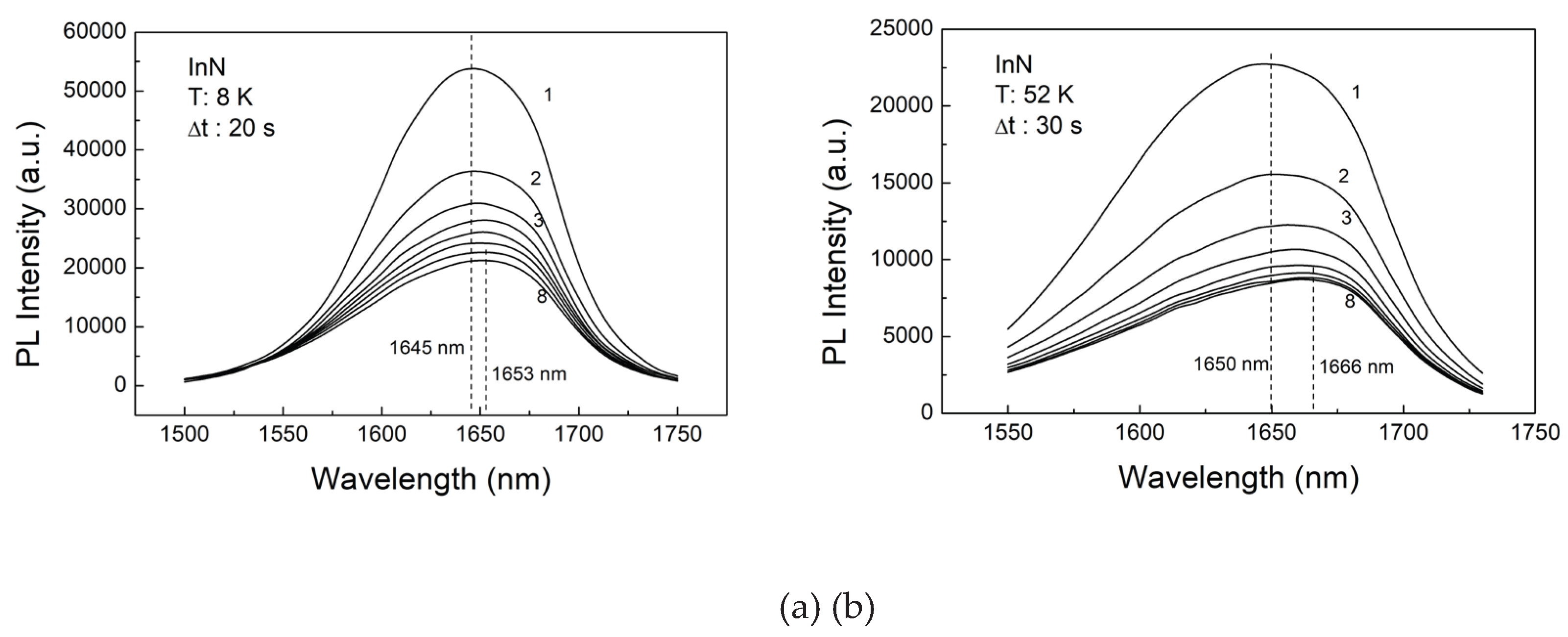
Figure 5.
Under continuous excitation, the variation curves of PL intensity with time at different temperatures.
Figure 5.
Under continuous excitation, the variation curves of PL intensity with time at different temperatures.
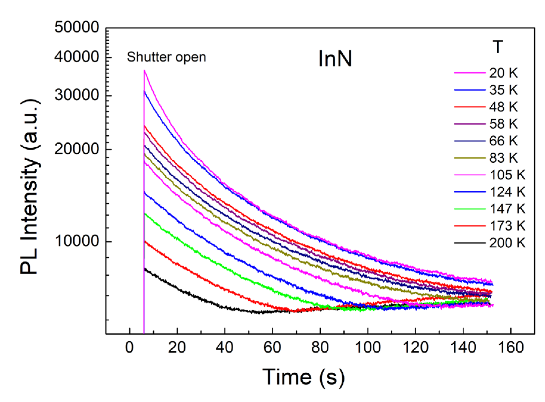
Figure 6.
Fitting results of the PL intensity decay curves at 20 K, 105 K and 200 K.
Disclaimer/Publisher’s Note: The statements, opinions and data contained in all publications are solely those of the individual author(s) and contributor(s) and not of MDPI and/or the editor(s). MDPI and/or the editor(s) disclaim responsibility for any injury to people or property resulting from any ideas, methods, instructions or products referred to in the content. |
© 2025 by the authors. Licensee MDPI, Basel, Switzerland. This article is an open access article distributed under the terms and conditions of the Creative Commons Attribution (CC BY) license (http://creativecommons.org/licenses/by/4.0/).
Copyright: This open access article is published under a Creative Commons CC BY 4.0 license, which permit the free download, distribution, and reuse, provided that the author and preprint are cited in any reuse.


