Submitted:
18 July 2025
Posted:
21 July 2025
You are already at the latest version
Abstract
The advent of graphene has catalyzed extensive exploration into two-dimensional (2D) materials, among which gallium selenide (GaSe) - a layered semiconductor - stands out for its promise in optoelectronic and nanoscale device applications. To elucidate the intricate correlation between structure and electronic properties, and to enable performance optimization at the atomic scale, we employ advanced characterization methodologies. In this work, atomic-resolution Scanning Transmission Electron Microscopy (STEM) and Electron Energy Loss Spectroscopy (EELS) are utilized to investigate the structural and electronic characteristics of GaSe. STEM imaging confirms the atomic-level uniformity and verifies the β-GaSe phase, while EELS measurements reveal a thickness-dependent, tunable bandgap that decreases from 3.8 eV to 2.4 eV as the crystal thickness increases from approximately 3 nm to 30 nm—a trend attributable to quantum confinement effects.
Keywords:
gallium selenide
; bandgap tunability
; scanning transmission electron microscopy
1. Introduction
The discovery of graphene in 2004 with the groundbreaking work of Geim and Novoselov [1], has revolutionized the field of two-dimensional (2D) materials, leading to extensive research into layered van der Waals (vdW) structures with unique electrical, optical, and mechanical properties [2,3]. These materials exhibit exceptional quantum confinement effects, tunable band structures, and strong light-matter interactions, making them attractive candidates for next-generation technologies [4,5]. In addition to graphene, other materials have gained significant attention due to their various optoelectronic applications, among them: transition metal semiconducting dichalcogenides (TMDs) and black phosphorus or indium-gallium chalcogenides [6], phosphorus or indium-gallium chalcogenides [7] In particular, GaSe, a layered semiconductor with a bandgap that varies with thickness, has emerged as a promising material for photodetectors, nonlinear optics [8], and flexible electronic devices [9].
Initial studies using few-layer GaSe in transistors [10] and photodetectors [11] have demonstrated its potential. Recent photoluminescence measurements on GaSe nanosheets [12] reveal high preservation of photon polarization between absorption and emission, highlighting its promise for spintronic applications. In addition, monolayer gallium selenide (GaSe) is a promising material for nanoscale electronic, spintronic, and optoelectronic applications [13], with its electrical and optical properties highly tunable through strain engineering, making the assessment of applied strain crucial. Furthermore, theoretical calculations indicate the potential for carrier-induced magnetism in single-layer GaSe [14].
GaSe’s unique properties stem from its anisotropic structure, consisting of covalently bonded layers held together by weak van der Waals forces. This configuration enables mechanical exfoliation and makes GaSe suitable for thin-film technologies. Its layered crystalline structure comprises four atomic planes (Se-Ga-Ga-Se) per layer, stacked along the c-axis. Bulk GaSe exists in four polytypes—β (2H), ε (2H′), γ (3R), and δ (2H-3R)—that correspond to different stacking arrangements [15]. Each polytype exhibits distinct optical and electronic properties, even at the same thickness, necessitating precise identification and characterization for application-specific uses. The modulation of optical properties based on thickness provides valuable opportunities for developing functional optoelectronic devices [16].
It is evident that GaSe has structural and electronic properties that make it a versatile material for 2D applications. The correlation between thickness, polytype and electronic behavior underscores the importance of detailed characterization. New advanced electron microscopy techniques are revolutionizing the characterization of two-dimensional materials like GaSe, enabling precise exploration of its structural and electronic properties. Aberration-corrected scanning transmission electron microscopy (STEM) allows for atomic-resolution imaging, which is crucial for distinguishing different polycrystalline phases of GaSe and detecting structural variations related to thickness [17].
Additionally, electron energy loss spectroscopy (EELS) combined with STEM enables the analysis of local electronic properties with nanometric spatial resolution, revealing changes in the density of electronic states as a function of layer number and polycrystalline configuration [18].
The integration of these advanced methodologies with theoretical models and atomistic simulations will open new avenues for engineering GaSe-based devices, optimizing their performance for applications in optoelectronics, plasmonics, and nonlinear optics. To investigate these properties, advanced characterization techniques such as Scanning Transmission Electron Microscopy (STEM) and Electron Energy Loss Spectroscopy (EELS) were employed. Using a JEM-ARM200F NEOARM transmission electron microscope operating at 200 kV, detailed insights into the crystal structure, morphology, and electronic behavior of GaSe were obtained.
High-angle annular dark-field (HAADF) imaging in STEM mode provided subatomic resolution, revealing the atomic arrangement of GaSe and confirming the β-GaSe structural modification.
2. Materials and Methods
High-purity gallium (99.999%) and selenium (99.999%) from Sigma Aldrich were used as starting materials. These elements were weighed in a stoichiometric 1:1 molar ratio and loaded into a cleaned quartz ampoule. The ampoule was then evacuated to a pressure of approximately 10−5 Torr and sealed to prevent contamination during the crystal growth process.
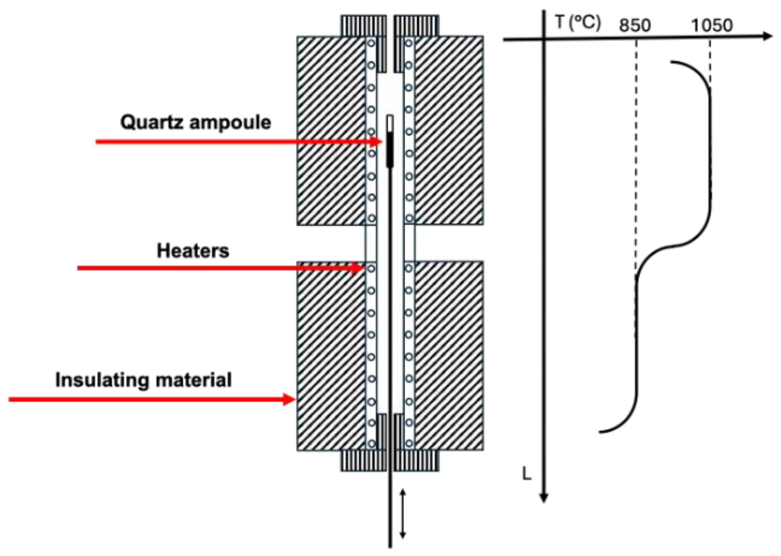
To promote initial reaction and homogenization, the sealed ampoule was optionally pre-reacted in a rocking furnace at 600 °C for 24 to 48 hours. After this step, the ampoule was placed vertically into a Bridgman-type furnace comprising a high-temperature zone (around 950–1000 °C), a low-temperature zone (approximately 400–500 °C), and a narrow intermediate region to establish a sharp thermal gradient. The schematic of the furnace used for the deposition, along with the corresponding thermal gradient between the different zones, is shown in the Figure 1.
The ampoule was initially held in the high-temperature zone until the GaSe charge was fully molten. Then, it was slowly lowered through the thermal gradient at a rate of 0.5 mm per hour. As the ampoule passed into the cooler region, directional solidification occurred from the pointed bottom of the ampoule upward, encouraging the growth of a single crystal along the direction of movement.
Once the crystallization was complete, the entire system was cooled gradually to room temperature to minimize thermal stress and avoid cracking of the crystal. The quartz ampoule was then broken open, and the GaSe ingot was extracted.
Bulk pieces of the material were initially mechanically exfoliated using a scalpel blade approximately 20 microns thick from the high-quality GaSe ingots synthesized and deposited in our laboratory according to the procedures detailed above. Subsequently, a top-down process was employed to exfoliate progressively thinner GaSe fragments down to single layers. This thinning method thoroughly preserves the structural integrity of the material. The resulting thin flakes were then mounted onto TEM grids for all TEM characterizations.
Figure 1.
Schematic representation of the vertical Bridgman method used for the growth of GaSe single crystals. The quartz ampoule containing stoichiometric Ga and Se is lowered through a controlled thermal gradient, promoting directional solidification and phase-pure crystal growth. The thermal profile and zone configuration are illustrated.
Scanning Transmission Electron Microscopy (TEM) and Electron Energy Loss Spectroscopy (EELS) were performed by a Jeol JEM-ARM 200F NEOARM operated at 200 kV to correlative morphological and electronic structure analysis.
To investigate the structural order of GaSe, high-angle annular dark field (HAADF) imaging was performed in scanning transmission electron microscopy (STEM) mode using an annular dark field detector. In this technique, a focused electron beam is scanned across the sample, and elastically scattered electrons at high angles (>50 mrad) are collected by the detector. The resulting signal intensity is approximately proportional to the square of the atomic number (Z2) of the scattering atoms, providing atomic number-sensitive contrast (Z-contrast). HAADF imaging minimizes contributions from diffraction effects, enabling high spatial resolution and direct compositional information at the atomic scale. For optimal imaging conditions, the convergence semi-angle of the electron probe was set to 30 mrad, and the detector’’s collection angle range was set between 50 and 100 mrad. Data acquisition was performed with a pixel dwell time of 20 μs and the images were processed using Digital Micrograph (DM) software to enhance contrast and reduce noise.
Energy-filtered transmission electron microscopy (EF-TEM) was employed to acquire energy-filtered images for improved contrast and detailed analysis of material composition at atomic resolution. Zero-loss filtering was utilized to enhance image contrast by excluding inelastically scattered electrons, while core-loss edge filtering allowed the generation of compositional maps with high spatial resolution.
Spectral imaging in scanning transmission electron microscopy (SI-STEM) was performed to analyze the electronic structure of our samples. In this technique, a focused electron beam was scanned across the sample in a raster pattern, and at each scan position, a spectrum was collected using an electron energy loss spectrometer (EELS). This method enables the simultaneous acquisition of spatial and spectral information, producing a hyperspectral data cube with two spatial dimensions and one spectral dimension. EELS spectra were recorded with an energy resolution of 50 meV over the 0-50 eV range to capture low-energy electronic transitions. To achieve a sufficient signal-to-noise ratio, a pixel dwell time of 2 ms was used during acquisition. The low-loss EELS spectrum (VEELS) provides critical information about valence electron excitations in the material. This spectral range includes key features such as:
- ▪
- Zero-Loss Peak (ZLP): A dominant peak at 0 eV, representing electrons that have not undergone inelastic scattering.
- ▪
- Plasmonic Excitations: Collective oscillations of free or weakly bound electrons, typically appearing as broad peaks at intermediate energy losses.
- ▪
- Interband Transitions: Features associated with electronic transitions between the valence and conduction bands, providing insight into the material’s electronic structure.
- ▪
- Bandgap Characteristics: The onset of energy loss intensity at specific energies, which allows estimation of the material’s bandgap and its dependence on thickness.
- Data processing was performed using Digital Micrograph (DM) software.
3. Results
Figure 2a presents a High-Angle Annular Dark Field (HAADF) image acquired from a very thin region of the GaSe sample, providing a direct visualization of the lattice structure. HAADF imaging, a scanning transmission electron microscopy (STEM) technique, exploits the Z-contrast effect, where heavier atoms scatter electrons more strongly than lighter ones. This results in brighter spots corresponding to regions with heavier elements, enabling a clear distinction between different atomic species based on their atomic number. In the case of GaSe, this contrast mechanism is particularly useful for identifying gallium (Ga) and selenium (Se) within the lattice and analyzing structural variations at the atomic scale. The Z-contrast observed in the HAADF image is fundamental in determining the arrangement of atomic columns, allowing for a detailed study of material properties such as stacking order, local defects, and layer thickness variations. Since GaSe is a layered van der Waals material, understanding its atomic structure is crucial for evaluating its electronic and optical properties. The high-resolution imaging provided by HAADF-STEM, combined with computational simulations, enables a comprehensive investigation of different structural modifications of the monolayer.
To further aid in the interpretation of the atomic arrangements, Figure 2b displays the simulated crystal structure of the β-GaSe structural modification, generated using VESTA [19]. VESTA is widely used for visualizing crystallographic structures and for analyzing interatomic distances, coordination environments, and bonding configurations. The inclusion of this theoretical model enables a direct comparison between expected and observed structural features, bridging the gap between computational predictions and experimental observations.
Figure 2c presents high-resolution simulated image of the GaSe monolayer, corresponding to the β-GaSe structural modification. The simulation performed using SIMULATEM [20], provides a powerful tool for generating STEM image simulations based on experimental parameters. By comparing these simulated images with experimental data, it is possible to validate structural models, identify potential distortions or defects, and gain deeper insight into the material’s behavior under different conditions.
These analyses are essential for exploring the polymorphism of GaSe, as structural variations can significantly impact its electronic band structure, carrier mobility, and optical properties. The ability to distinguish different GaSe modifications at the atomic scale provides valuable insights for tailoring the material’s characteristics for specific applications, such as in optoelectronic devices, photodetectors, and nanoscale transistors.
By integrating HAADF imaging with advanced simulations, this study offers a robust framework for characterizing the atomic structure of GaSe, highlighting the importance of combining experimental and theoretical approaches to understand and manipulate two-dimensional materials.
Figure 3a,b present a zero-loss high-resolution transmission electron microscopy (HRTEM) image of an ultrathin gallium selenide (GaSe) sheet obtained using energy-filtered transmission electron microscopy (EF-TEM), and a corresponding enlargement of the circled region, respectively. The zero-loss filtering technique selectively removes inelastically scattered electrons, which typically contribute to background noise and reduce image contrast. By filtering out these electrons, the resulting image provides improved structural clarity, allowing for a more precise visualization of atomic arrangements within the material. This technique is particularly valuable for examining delicate, nanoscale materials like GaSe, where maintaining high contrast and resolution is crucial for accurate structural characterization.
In this context, the zero-loss HRTEM image offers a contrast mechanism like the HAADF image discussed earlier. Both techniques enhance the visibility of atomic features, albeit through different mechanisms HAADF imaging relies on atomic number (Z-contrast) variations, while EF-TEM selectively removes energy-loss contributions to refine structural details. The improved contrast in the zero-loss image enables better distinction between individual GaSe layers, facilitating the analysis of structural defects, layer stacking, and local thickness variations.
To complement the structural imaging, Figure 3c,d present the corresponding composite elemental map, illustrating the spatial distribution of gallium (Ga) and selenium (Se) within the thin film, and a corresponding enlargement of the circled region, respectively. This map was generated by selecting the characteristic energy absorption edges of Se M4,5 and Ga M2,3, ensuring precise elemental differentiation. In the composite representation, selenium is depicted in red, while gallium appears in green, providing an intuitive visualization of the material’s composition.
The elemental mapping technique employed here is particularly useful for identifying inhomogeneities, defects, and potential segregation of elements within the sample. Given that GaSe is a van der Waals material with strong in-plane bonding and weak interlayer interactions, slight variations in stoichiometry or elemental distribution can significantly influence its electronic and optical properties. The detailed spatial distribution of gallium and selenium observed in Figure 2b provides valuable insight into the material’s uniformity, structural integrity, and potential deviations from ideal stoichiometry, which could affect device performance in optoelectronic applications.
By combining zero-loss HRTEM imaging with energy-filtered elemental mapping, this analysis provides a comprehensive characterization of the GaSe thin film at the nanoscale. The synergy between these techniques allows researchers to establish a direct link between the structural and compositional properties of the material, paving the way for a deeper understanding of its physical behavior and potential technological applications in nanodevices and photonic systems.
At medium magnification, the GaSe sample reveals its characteristic terraced structure, as shown in Figure 4a. These terraces arise due to the layered nature of GaSe, a van der Waals material composed of weakly bonded atomic sheets. The step-like morphology plays a significant role in influencing the electronic behavior of the material, as variations in layer thickness can modify local electronic states. Understanding these structural variations is crucial for applications in optoelectronics and nanodevices, where precise control over electronic properties is required.
The terraced structure serves as an ideal system for studying the correlation between morphology and electronic properties using Electron Energy Loss Spectroscopy (EELS). EELS provides detailed information on energy loss mechanisms as electrons interact with the sample, making it a powerful tool for probing local electronic structure, bandgap variations, and plasmonic excitations. Since electronic properties in GaSe are highly sensitive to thickness, EELS measurements across different terrace levels allow for the identification of trends in bandgap energy, electronic transitions, and dielectric response.
Figure 4 highlights the relationship between the morphological features (picture b) observed in the HAADF mode and the quantitative electronic structure analysis performed via EELS (picture c). The HAADF mode, which is sensitive to atomic number (Z-contrast), helps in distinguishing regions of different thicknesses within the sample. By selecting specific areas in the HAADF image for EELS measurements, one can extract precise spectral data corresponding to varying structural configurations. This correlation enables a deeper understanding of how morphological characteristics—such as terrace height, strain effects, and local defects—influence the electronic response of GaSe.
In the analyzed area, the material exhibits a thickness variation ranging from 4 to 30 nm, forming eight distinct terraces. Each terrace measures approximately 5 nm in height and 20 nm in lateral dimension, corresponding to 1000 image points in the dataset. This structured variation in thickness provides an excellent platform for studying how electronic properties evolve as a function of material thickness. By averaging Electron Energy Loss Spectroscopy (EELS) spectra over each terrace, statistically significant trends can be observed, offering insights into the thickness-dependent behavior of GaSe.
To accurately analyze the valence electron region, the zero-loss peak was subtracted (for detail see supplementary material). Figure 5a presents the EELS spectra obtained from the different regions identified in Figure 4, highlighting thickness-dependent variations in low-energy electronic excitations. The intensity melemriodulation observed in the low-loss EELS spectrum reveals distinct features corresponding to electron energy loss events due to interactions within the GaSe sample.
The spectra reveal distinct profiles characterized by two prominent peaks, located at approximately 6 eV and 16 eV, which offer valuable insight into the electronic properties of GaSe. The peak at 6 eV becomes increasingly pronounced in regions where the thickness exceeds 20 nm, suggesting a growing contribution from collective electronic excitations such as interband transitions and plasmonic resonances. This enhanced intensity at greater thicknesses implies a reduction in quantum confinement effects, allowing a higher density of electronic states to participate in excitation processes. In contrast, the peak at 16 eV remains consistently present across all thicknesses, indicating that it corresponds to a fundamental electronic excitation intrinsic to GaSe.
Figure 5b presents a zoomed-in view of the absorption edge region, revealing a clear thickness-dependent behavior. As the GaSe layer becomes thicker, the onset of the absorption edge progressively shifts toward lower energies. This redshift is attributed to the gradual suppression of quantum confinement effects, which significantly affect the electronic structure in ultrathin layers.
The experimental data points corresponding to the optical absorption edge are highlighted in Figure 5b and plotted as a function of material thickness in Figure 6. The observed trend suggests a possible dependence of the energy band gap on thickness of the form:
where E0 denotes the band gap in the bulk limit, and A and n are fitting parameters that account for the strength and dimensionality of the confinement effects. This phenomenological expression has been widely adopted in the literature to describe confinement-induced shifts in the energy gap of layered semiconductors [21,22].
However, this empirical model is too simplified to fully capture the complexity of the underlying physical phenomena. Typically, the exponent n is close to 2; however, our experimental data yield a value near 0.3. Although the 1/dn dependence captures the general trend of gap widening with decreasing thickness, the fitted n deviates markedly from the ideal value of 2 predicted by the infinite square quantum well model within the effective mass approximation [23], where the confinement-induced energy shift follows:
where me∗ and mh∗ are the effective masses of electrons and holes, respectively. The deviation from this ideal behavior suggests that simple quantum confinement cannot fully account for the experimental observations in few-layer GaSe. Rather, the reduced exponent likely reflects a more complex interplay of physical mechanisms beyond particle-in-a-box quantization.
Interestingly, the fitted exponent n≈0.3 is numerically close to the reported in-plane effective mass ratio m∗/m0≈0.3 for carriers in GaSe [24]. However, this numerical similarity should not be overinterpreted as a direct physical correspondence. In the absence of a rigorous theoretical model that explicitly links the exponent n to the effective mass, such parallels remain speculative and primarily serve to indicate the presence of strong quantum size effects in the system.
Density functional theory (DFT) calculations support the interpretation of a thickness-dependent band structure evolution in GaSe, with a predicted widening of the band gap in the few-layer limit due to dimensional confinement [25]. As the number of layers decreases, the out-of-plane carrier motion becomes restricted, resulting in the discretization of energy levels and a shift of the conduction and valence band edges. This behaviour is consistent with what has been observed in other van der Waals materials such as MoS2, where a monolayer exhibits a direct band gap, while bulk MoS2 exhibits an indirect gap due to altered electronic band dispersion [26].
Beyond quantum confinement, additional factors contribute to the modulation of the band gap with thickness. One such mechanism is the variation in dielectric screening. In ultrathin GaSe, the reduced dimensionality weakens the ability of the material to screen Coulomb interactions, leading to enhanced exciton binding energies and a concomitant increase in the optical gap [27,28]. As thickness increases, dielectric screening becomes more effective, lowering exciton binding energies and contributing to a redshift of the absorption edge.
Moreover, interlayer coupling plays a significant role in the electronic structure of GaSe. Although the layers are bound by van der Waals forces, their interaction is non-negligible and can lead to hybridization of electronic states, especially in thicker samples. This coupling alters band dispersion and contributes to the observed narrowing of the gap with increasing layer number [29]. Similar effects have been reported in layered InSe, where the optical band gap is highly sensitive to the number of layers due to strong interlayer interactions [30].
To more accurately describe the experimental trends and account for the multifaceted nature of thickness-dependent band gap evolution in GaSe, it is necessary to go beyond the simple confinement model. A refined description that incorporates additional physical effects—including dielectric screening and interlayer electronic coupling—can be formulated as:
In this model, the first term represents quantum confinement, the second captures interlayer coupling effects (which decay exponentially with increasing thickness), and the third accounts for dielectric screening, with ε(d) describing the thickness-dependent dielectric environment. [31]
The thickness-dependent dielectric permittivity of GaSe can be described using a phenomenological model of the form:
where ε(d) is the effective dielectric constant as a function of thickness d, ε∞ is the bulk dielectric constant, α is a dimensionless parameter describing the suppression of screening at low thickness, and d0 is a characteristic screening length scale.
Using this expression, the relative dielectric constant for a monolayer (d→0) is estimated as:
while in the bulk limit (d→∞), it converges to ε∞≈8.0, in good agreement with both DFT calculations and optical spectroscopy data. Based on available literature, it is reasonable to assume that α≈0, accounting for the reduced dielectric screening in atomically thin layers. The characteristic screening length is estimated as d0≈3.2 nm, which corresponds approximately to four GaSe layers [32].
Here, the parameter λ represents a characteristic decay length associated with interlayer coupling. In layered van der Waals materials such as GaSe, although the individual layers are primarily held together by weak non-covalent forces, their electronic states can still hybridize across adjacent layers. This interlayer interaction modifies the band dispersion and becomes increasingly significant in thicker samples. The effect of such coupling on the electronic structure typically diminishes with increasing thickness and is well described by an exponential decay. The parameter λ therefore quantifies the spatial range over which interlayer electronic interactions remain effective. Physically, it reflects the extent to which electronic wavefunctions from adjacent layers overlap in the out-of-plane direction. A small λ implies that interlayer coupling is strongly localized, while a larger λ indicates more delocalized interlayer interactions. [33] For GaSe and related semiconductors, typical values of λ lie in the range of a few nanometers, corresponding to several atomic layers. Figure 7 shows the energy gap as a function of thickness, where, in addition to the experimental data for thin layers obtained from EELS measurements, we have included the bulk energy gap values derived from optical measurements using UV-Vis-NIR spectroscopy. Further details on these measurements are provided in the supplementary material of the paper. The equation accurately fits the experimental data across the entire thickness range, capturing both the quantum confinement effects at low thickness and the asymptotic behavior in the bulk limit. The corresponding fitting parameters are summarized in the Table 1.
5. Conclusions
In this work, we have conducted a comprehensive structural and electronic investigation of gallium selenide (GaSe) thin films, spanning a wide range of thicknesses. By integrating high-resolution electron microscopy, energy-filtered imaging, elemental mapping, and electron energy loss spectroscopy (EELS) with advanced simulations and theoretical modeling, we have gained deep insights into the nanoscale characteristics of this layered material.
Atomic-resolution imaging via HAADF-STEM and zero-loss HRTEM enabled direct observation of the crystalline arrangement in ultrathin GaSe, revealing critical features such as stacking sequences, local structural imperfections, and terraced morphology. These observations were corroborated by simulated HAADF images and atomistic models, providing a robust basis for the identification of structural polymorphs and validating theoretical structural predictions.
Complementary EF-TEM elemental mapping offered a spatially resolved view of gallium and selenium distribution, affirming the compositional uniformity of the samples and highlighting the synergy of structural and chemical imaging in characterizing van der Waals materials.
EELS analyses performed across discrete terraced regions uncovered a clear thickness dependence in the electronic response of GaSe. The progressive evolution of the low-loss spectra, particularly the behavior of features at ~6 eV and ~16 eV, underscored the transition from quantum-confined to bulk-like regimes. The increasing intensity of the 6 eV feature with thickness pointed to enhanced plasmonic and interband excitation contributions in thicker layers.
A detailed examination of the optical band gap as a function of thickness revealed significant deviations from the predictions of the conventional inverse-square confinement model. Instead, the data are better described by an extended model incorporating quantum confinement, thickness-dependent dielectric screening, and interlayer coupling effects. This refined analytical approach successfully captures both the low-thickness behavior and the asymptotic trend toward the bulk gap.
Key parameters extracted from the fitting—such as a reduced confinement exponent (n ≈ 0.3), a dielectric screening length (d0 ≈ 3.2 nm), and an interlayer coupling decay constant (λ)—align well with values reported in theoretical and experimental literature. These findings emphasize the importance of considering not only geometrical confinement but also the complex interplay of electronic screening and interlayer hybridization when modeling the electronic structure of GaSe.
Altogether, this study offers a detailed, multi-faceted understanding of how structural and electronic properties of GaSe evolve with layer thickness. The combined use of advanced microscopy, spectroscopy, and modeling establishes a powerful methodological framework for investigating two-dimensional semiconductors. These insights are crucial for guiding the design of GaSe-based optoelectronic and photonic devices, where precise control over thickness, structure, and electronic properties is essential. Future investigations targeting excitonic dynamics, strain effects, and substrate interactions may further unlock the potential of GaSe and related layered materials for next-generation technologies.
Supplementary Materials
The following supporting information can be downloaded at the website of this paper posted on Preprints.org.
Author Contributions
Conceptualization, A.S. and D.M.; methodology, X.X.; software, X.X.; validation, X.X., Y.Y. and Z.Z.; formal analysis, X.X.; investigation, L.M. and A.B.; resources, L.C.; data curation, A.S., D.M., L.M. and A.B.; writing—original draft preparation, A.S. and D.M.; writing—review and editing, A.S. and D.M.; visualization, A.S. and D.M; supervision, A.S. and D.M; project administration, L.C., A.S. and D.M; funding acquisition, L.C. All authors have read and agreed to the published version of the manuscript.
Funding
This research was supported by the Italian government under the PNRR and by the Platform for CERIC-ERIC Upgrade PRP@CERIC Project (Prot IR0000028, CUP J97G22000400006) funded by European Union-NextGenerationEU.
Data Availability Statement
The original contributions presented in this study are included in the article. Further inquiries can be directed to corresponding authors.
Conflicts of Interest
The authors declare no conflicts of interest.
Abbreviations
The following abbreviations are used in this manuscript:
| DFT | Density Functional Theory |
| EELS | Electron Energy Loss Spectroscopy |
| EF-TEM | Energy Filtered Transmission Electron Microscopy |
| HAADF | High-angle annular dark-field |
| HRTEM | High Resolution Transmission Electron Microscopy |
| SI-STEM | Spectral Imaging In Scanning Transmission Electron Microscopy |
| STEM | Scanning Transmission Electron Microscopy |
| TEM | Transmission Electron Microscopy |
| VEELS | Valence Electron Energy Loss Spectrum |
| ZLP | Zero-Loss Peak |
References
- Novoselov, K.S. , Geim A.K., Morozov S.V., Electric Field Effect in Atomically Thin Carbon Films, Science306 (2004) 666–669.
- Lin YC, Torsi R, Younas R, Hinkle CL, Rigosi AF, Hill HM, Zhang K, Huang S, Shuck CE, Chen C, Lin YH, Maldonado-Lopez D, Mendoza-Cortes JL, Ferrier J, Kar S, Nayir N, Rajabpour S, van Duin ACT, Liu X, Jariwala D, Jiang J, Shi J, Mortelmans W, Jaramillo R, Lopes JMJ, Engel-Herbert R, Trofe A, Ignatova T, Lee SH, Mao Z, Damian L, Wang Y, Steves MA, Knappenberger KL Jr, Wang Z, Law S, Bepete G, Zhou D, Lin JX, Scheurer MS, Li J, Wang P, Yu G, Wu S, Akinwande D, Redwing JM, Terrones M, Robinson JA. , Recent Advances in 2D Material Theory, Synthesis, Properties, and Applications. ACS Nano. 2023, 17, 9694–9747. [CrossRef]
- Nirmal, K.A. , Kumbhar, D.D., Kesavan, A.V. et al. Advancements in 2D layered material memristors: unleashing their potential beyond memory. npj 2D Mater Appl 8, 83 (2024). [CrossRef]
- Zeng Wang, Kandammathe Valiyaveedu Sreekanth, Meng Zhao, Jinpeng Nong, Yincheng Liu, Jinghua Teng, Two-dimensional materials for tunable and nonlinear metaoptics[J]. Advanced Photonics, 2024, 6, 034001.
- Qi, L. , Xu T. , Xing Z., Chen S., Zhang Z., Liu T.,and Cheng Z., Mid-Infrared Optoelectronic Waveguide Devices with 2DMaterials Adv. Physics Res. 2025, 4, 2400079. [Google Scholar]
- Ryder C., R. , Wood J. D., Wells S. A. and Hersam M. C., Chemically Tailoring Semiconducting Two-Dimensional Transition Metal Dichalcogenides and Black Phosphorus. ACS Nano 2016, 10, 3900−3917. [Google Scholar]
- Arora, H. , Erbe A. , Recent progress in contact, mobility, and encapsulationengineering of InSe and GaSe. Info Mat. 2021, 3, 662–693. [Google Scholar]
- Song, M. , An N. , Zou Y., Zhang Y., Huang W., Hou H.i, Chen X.i., Epitaxial growth of 2D gallium selenide flakes for strong nonlinear optical response and visible-light photodetection. Front. Phys. › 2023, 18, 52302. [Google Scholar] [CrossRef]
- Barker, T. , Gray A., Weir M.P., Sharp J.S., Kenton, A., Kudrynskyi Z.R., Rostami H., Patané A., Giant elasto-optic response of gallium selenide on flexible mica, Npj Flex. Electron. 9 (2025) 1–5. [CrossRef]
- Late, D.J. , Liu B. Mater. 24 (2012) 3549–3554. [CrossRef]
- Cao, Y. , Cai K., Hu P., Zhao L., Yan T., Luo W., Zhang X., Wu X., Wang K., Zheng H., Strong enhancement of photoresponsivity with shrinking the electrodes spacing in few layer GaSe photodetectors, Sci. Rep. 5 (2015) 1–7. [CrossRef]
- Del Pozo-Zamudio, O. , Schwarz S., Sich M., Akimov I.A., Bayer M., Schofield R.C., Chekhovich E.A., Robinson B.J., Kay N.D., Kolosov O. V., Dmitriev A.I., Lashkarev G.V., Borisenko D.N., Kolesnikov N.N., Tartakovskii A.I., Photoluminescence of two-dimensional GaTe and GaSe films, 2D Mater. 2, 035010 (2015). [CrossRef]
- Longuinhos, R. and Ribeiro-Soares J., Monitoring the Applied Strain in Monolayer Gallium Selenide through Vibrational Spectroscopies: A First-Principles Investigation. Phys. Rev. 0240; 11. [Google Scholar]
- Hao, H.G. , Ran X., Tang Y., Zheng S., Ruan W., A Single-Layer Focusing Metasurface Based on Induced Magnetism, Prog. Electromagn. Res. 172, 77–88 (2021). [CrossRef]
- Ni, Y. , Wu H., Huang C., Mao M., Wang Z., Cheng X., Growth and quality of gallium selenide (GaSe) crystals, J. Cryst. Growth. 381 10–14 (2013).
- Lim S., Y. , Lee J.U., Kim J.H., Liang L., Kong X., Nguyen T. T. H., Lee Z., Chof S., Cheong H., Polytypism in few-layer gallium selenide. Nanoscale, 2020, 12, 8563–8573.
- Pennycook, S.J. , Chisholm M.F., Lupini A.R., Varela M., Borisevich A.Y., Oxley M.P., Luo W.D., van Benthem K., Oh S.-H., Sales D.L., Molina S.I., García-Barriocanal J., Leon C., Santamaría J., Rashkeev S.N., Pantelides S.T., Aberration-corrected scanning transmission electron microscopy: from atomic imaging and analysis to solving energy problems, Phil. Trans. R. Soc. A 367, 3709–3733 (2009). [CrossRef]
- Azizi, A. , Antonius G., Regan E., Eskandari R., Kahn S., Wang F., Louie S.G., Zettl A., Layer-dependent electronic structure of atomically resolved two-dimensional gallium selenide telluride, Nano Lett. 19, 1782–1787 (2019). [CrossRef]
- Momma, K. and Izumi F., VESTA 3 for three-dimensional visualization of crystal, volumetric and morphology data, J. Appl. Cryst. 1272; 44. [Google Scholar] [CrossRef]
- Gomez-Rodríguez, A. , Beltran-del-Río L.M., R. Herrera-Becerra R. M: SimulaTEM, 2010. [Google Scholar] [CrossRef]
- Yi Zhang, Tay-Rong Chang, Bo Zhou, Yong-Tao Cui, Hao Yan, Zhongkai Liu, Felix Schmitt, James Lee, Rob Moore, Yulin Chen, Hsin Lin, Horng-Tay Jeng, Sung-Kwan Mo, Zahid Hussain, Arun Bansil, Zhi-Xun Shen, Direct observation of the transition from indirect to direct bandgap in atomically thin epitaxial MoSe2, Nat. Nanotechnol. 9, 111–115 (2014). [CrossRef]
- Kylänpää I, Komsa H.P., Binding energies of exciton complexes in transition metal dichalcogenide monolayers and effect of dielectric environment, Phys. Rev. B 92, 205418 (2015). [CrossRef]
- Bastard, G. , Wave Mechanics Applied to Semiconductor Heterostructures. John Wiley and Sons Inc., 1990.
- Mooser, E. , Il Nuovo Cimento B 1973, 18, 1–15.
- Leu P., W. , Shan B., & Cho K., Surface chemical control of the electronic structure of silicon nanowires: Density functional calculations Phys. Rev. B 73, 195320 (2006). [CrossRef]
- Zhang, L. & Zunger, A., Nano Lett. 15, 949–957 (2015).
- Ugeda M., M. Bradley A.J., Shi S.F., da Jornada F.H.,.Zhang Y, Qiu D.Y., Ruan W., Mo S.K., Hussain Z., Shen Z.X., Wang F., Louie S.G., Crommie M.F., Giant bandgap renormalization and excitonic effects in a monolayer transition metal dichalcogenide semiconductor. Nat. Mater. 2014, 13, 1091–1095. [Google Scholar] [CrossRef]
- Raja, A. , Chaves A., Yu J., Arefe G., Hill H. M., Rigosi A.F., Berkelbach T. C., Nagler P., Schüller C., Korn T., Nuckolls C., Hone J., Brus L. E., Heinz T. F., Reichman D. R., Chernikov A., Coulomb engineering of the bandgap and excitons in two-dimensional materials, Nature Communications 8, 15251 (2017).
- Rybkovskiy D., V. , Osadchy A. V., Obraztsova E. D., Transition from parabolic to ring-shaped valence band maximum in few-layer GaS, GaSe, and InSe, Physical Review B 2014, 90, 235302. [CrossRef]
- Sun, Y. , Luo S., Zhao X.G., Biswas K., Li S.L., Zhang L., InSe: a two-dimensional material with strong interlayer coupling, Nanoscale 10, 7991–7998 (2018). [CrossRef]
- Sun, M. , Huang, B., Thickness-dependent dielectric constant of few-layer In2Se3 nanoflakes. Nano Letters, 15, 6300–6304 (2015). [CrossRef]
- Guo, Q. , Su G., Liu J., Zhang Z., Optical properties and excitonic effects in layered GaSe from first-principles, Physical Review B, 99, 115201 (2019). [CrossRef]
- Jia, F. , Tang Z., Cruz G. J., Gao W., Xu S., Ren W., Zhang P., Quasiparticle and excitonic structures of few-layer and bulk GaSe: Interlayer coupling, self-energy, and electron-hole interaction, Phys. Rev. Applied 21, 054019 (2024). [CrossRef]
Figure 2.
(a) HAADF-STEM image of a very thin GaSe region, highlighting the lattice structure with Z-contrast, where heavier atoms appear as brighter spots due to stronger electron scattering (b) show the corresponding b-GaSe structural modifications modeled with VESTA, providing a direct comparison between theoretical atomic arrangements and simulated imaging results. (c) High-resolution simulated HAADF images of monolayer GaSe for b-GaSe structural modifications, generated by Simulatem.
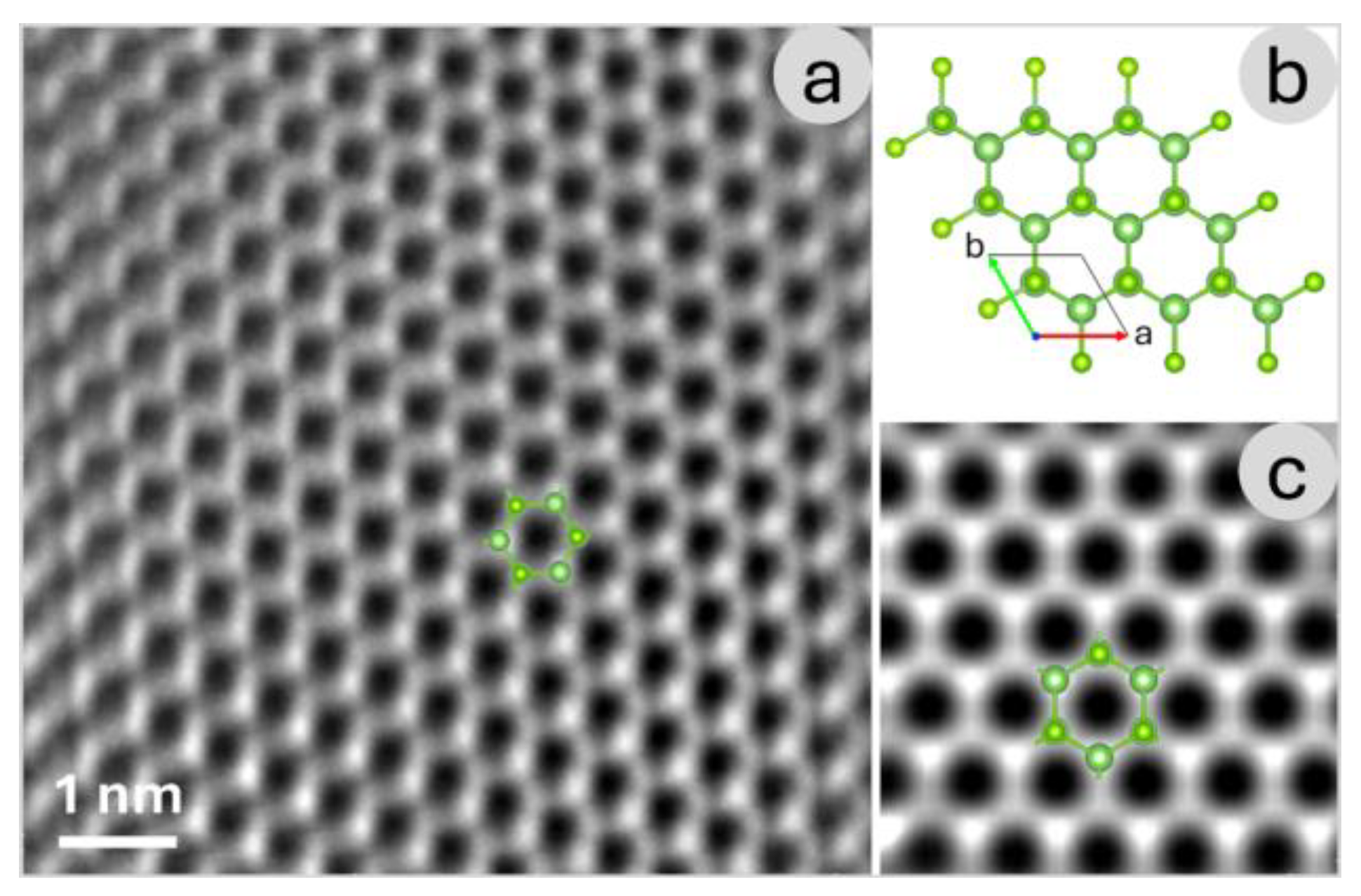
Figure 3.
(a) Zero-loss HRTEM image of an ultrathin GaSe sheet acquired using EF-TEM, where inelastically scattered electrons are filtered out to enhance structural clarity and contrast. (b) Enlargement of the circled region in (a). (c) Corresponding composite elemental map showing the spatial distribution of gallium (green) and selenium (red), generated by selecting the Se M4,5 and Ga M2,3 absorption edges, providing insight into the material’s composition and uniformity. (d) Enlargement of the circled region in (c).
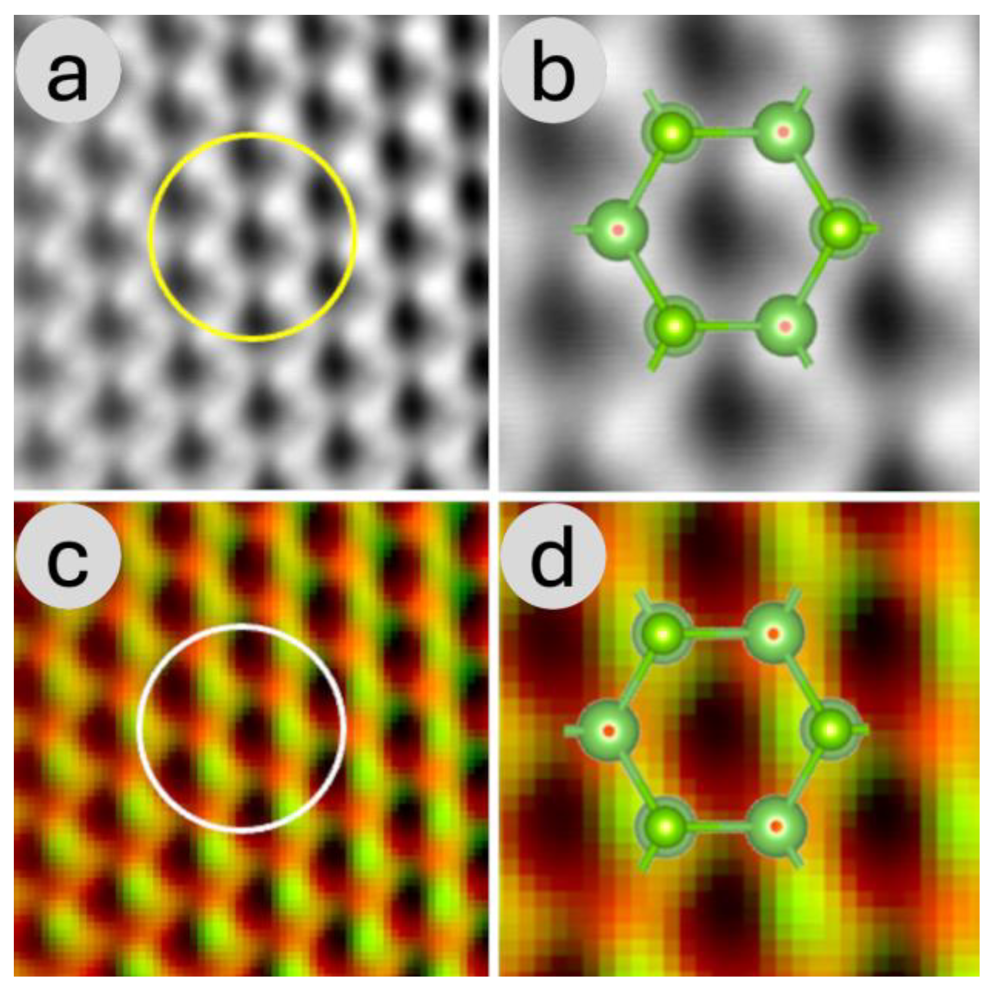
Figure 4.
(a) GaSe sample at medium magnification, displaying its characteristic terraced structure; the region highlighted in green indicates the area where SI-STEM analysis was performed. (b) HAADF image of the selected region, where the varying shades of gray indicate differences in thickness. (c) Quantitative thickness evaluation derived from electron energy loss spectroscopy (EELS) analysis; the white line represents the thickness profile measured along the AA’ line.
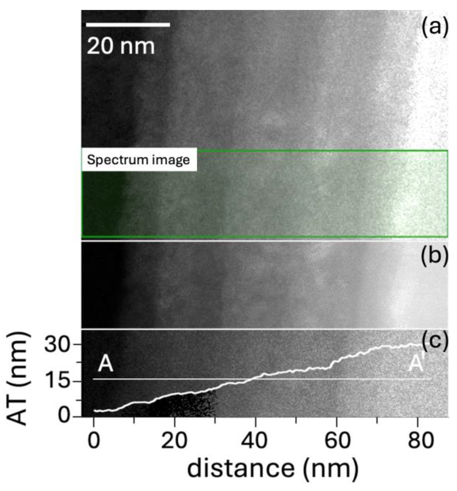
Figure 5.
(a) EELS spectra acquired from the regions identified in the previous figure (Figure 4), after subtraction of the zero-loss peak, showing variations in low-energy electronic excitations as a function of thickness. (b) Zoom into the absorption edge region, which also exhibits thickness-dependent behavior.
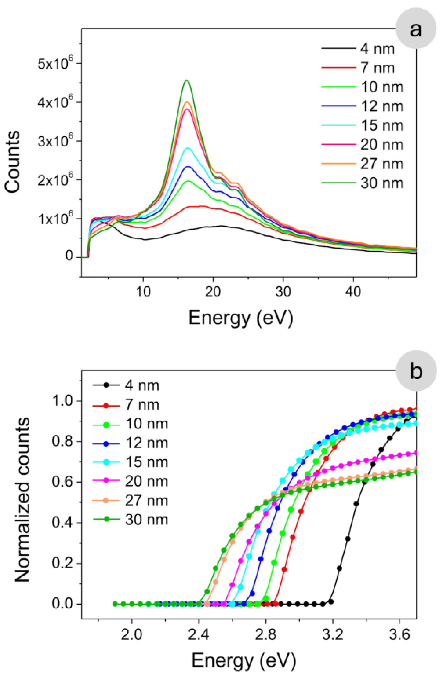
Figure 6.
Optical absorption edge plotted as a function of material thickness and fitted by a simple power low.
Figure 6.
Optical absorption edge plotted as a function of material thickness and fitted by a simple power low.
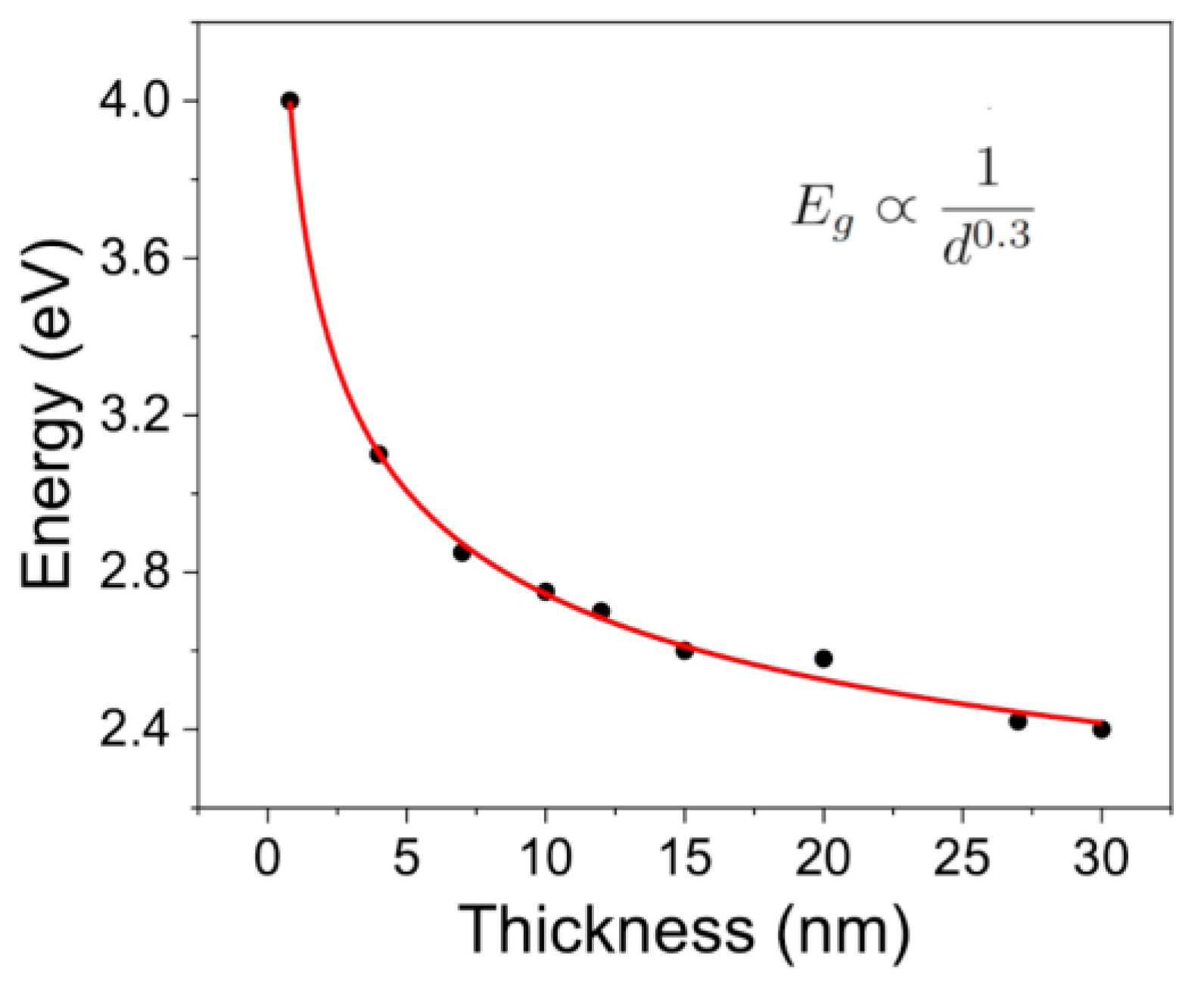
Figure 7.
Energy gap as a function of thickness. In addition to the experimental EELS data for thin layers, the plot includes the bulk energy gap values derived from UV-Vis-NIR spectroscopy. The fitting curve accounts for both quantum confinement and dielectric screening effects.
Figure 7.
Energy gap as a function of thickness. In addition to the experimental EELS data for thin layers, the plot includes the bulk energy gap values derived from UV-Vis-NIR spectroscopy. The fitting curve accounts for both quantum confinement and dielectric screening effects.
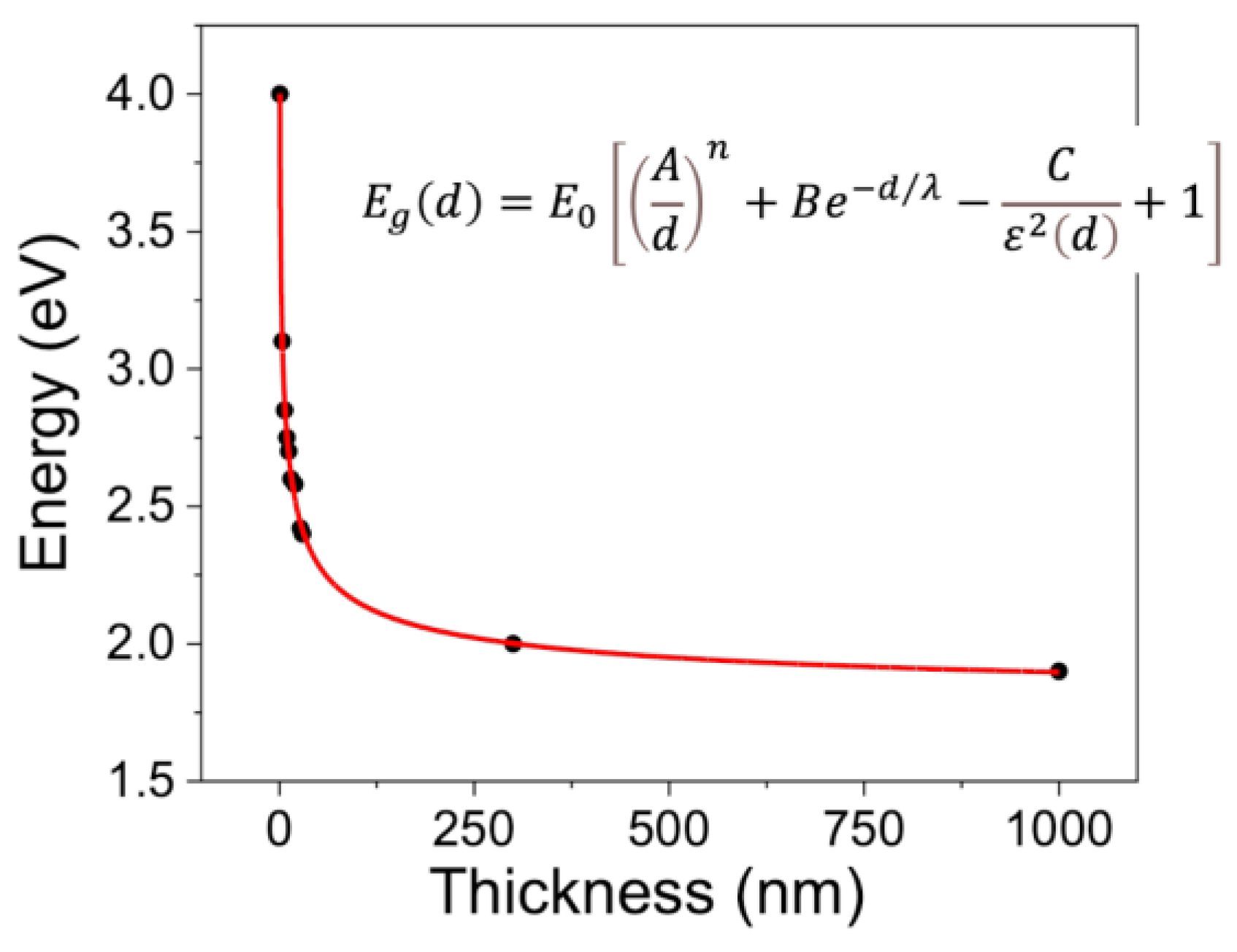

Table 1.
Fitting parameters.
| Parameters | Values | Standard error |
|---|---|---|
| E0 | 1.9 eV | 0.2 |
| A | 2.6 | 0.3 |
| B | 0.20 | 0.05 |
| C | 21 | 4 |
| l | 6 nm | 1 |
| n | 0.39 | 0.01 |
Disclaimer/Publisher’s Note: The statements, opinions and data contained in all publications are solely those of the individual author(s) and contributor(s) and not of MDPI and/or the editor(s). MDPI and/or the editor(s) disclaim responsibility for any injury to people or property resulting from any ideas, methods, instructions or products referred to in the content. |
© 2025 by the authors. Licensee MDPI, Basel, Switzerland. This article is an open access article distributed under the terms and conditions of the Creative Commons Attribution (CC BY) license (http://creativecommons.org/licenses/by/4.0/).
Copyright: This open access article is published under a Creative Commons CC BY 4.0 license, which permit the free download, distribution, and reuse, provided that the author and preprint are cited in any reuse.


