Submitted:
09 July 2025
Posted:
10 July 2025
You are already at the latest version
Abstract
New bulk chalcogenides from the system (GeTe6)1-xCux, where x=5, 10, 15 и 20 mol %, has been synthesized. The structure and composition of the materials was studied using X-ray powder diffraction (XRD) and energy dispersive spectroscopy (EDS). Scanning electron microscopy (SEM) has been applied to analyze the surface morphology of the samples. Some thermal characteristics as glass transition, crystallization and melting temperature and some physicochemical properties as density, compactness, molar and free volume were also determined. The XRD pattern shows sharp diffraction peaks indicating that the synthesized new bulk materials are crystalline. The following four crystal phases were determined: Te, Cu, CuTe и Cu2GeTe3. The results from the EDS confirm the presence of Ge, Te and Cu in the bulk samples in a concentration in good correspondence with those theoretically determined.
A layered thin film material based on the synthesized new Ge14Te81Cu5 chalcogenide, which has the most flexible structure, and the azo polymer PAZO has been fabricated, and the kinetic of the photoinduced birefringence at 444 nm has been measured. The results indicate an increase in the maximal induced birefringence for the layered structure in comparison to the non-doped azo polymer film.
Keywords:
transition metal doped chalcogenides
; azo polymers
; Ge-Te-Cu
1. Introduction
Among the chalcogen family, tellurium-based are of special interest as they demonstrate industrial valuable phase transition by being heated through an electrical current [1] or upon irradiation with light [2], which has already been used in rewriteable optical discs [3] and electronic 3D memory chips [4]. Since the commercialization of the GeSbTe [5] and of the AgInSbTe [6] as information storage media, many investigations have been carried out in order to improve the optical and electrical contrasts between the crystalline and glassy phase, to increase the number of reversible phase transitions, etc. A lot of them involve synthesis of Ge-Sb-Te or quaternary alloy (Ag, In)-doped Sb2Te with different concentrations of constituent elements [7,8], adding of dopants [9], introduction of Se and/or S into the matrix [10], incorporation of another chemical element in place of Sb [11,12]. Regarding the latter, it was reported by Y. Sutou et al that the crystallization starting time of an amorphous GeCu2Te3 film is as fast as that of an amorphous GeSbTe film, but it can be re-amorphized by laser irradiation at lower power and shorter pulse [13]. Dongol et al synthesized Ge-Te-Cu bulk glassies with higher thermal stability compared to the Ge-Sb-Te system [14]. Furthermore, it was found that Cu−Ge−Te alloys exhibit smaller density change upon crystallization and the crystalline phase has a lower optical reflectivity than the amorphous one [15,16]. The observed results have been attributed the to the copper d-electrons giving rise to different nature of the bonding between the structural units in amorphous and crystalline phase compared to the p-bonded chalcogenides [17]. Since, Ge-Te based chalcogenides doped with transition-metal have gathered attention as previously overlooked and underexplored materials for optoelectronic application. Many other interesting properties has also been reported for the Ge-Te-Cu system including resistance to oxidation, relatively high electrical conductivity, low heat conductivity, high Seebeck coefficient, high transmittance, low absorbance, and reflectance in the visible/near-infrared region, but high absorbance in the ultraviolet region [18]. In last years, a significant scientific effort has also been paid on the development of composite or hybrid materials combining the advantages of the chalcogenides with those of other materials [19,20,21]. An attractive class among them represent the azo dyes or polymers with embedded chalcogenide particles or prepared as multilayer structures, where the optical recording capability of the azo chromophores has been significantly enhanced after incorporation of the nanoparticles into the polymer matrix or as result of interface effects between the stacked films [22,23].
In the present article we report on the synthesis of new chalcogenides from the system Ge-Te-Cu, their structural investigation and determination of some physico-chemical properties. Furthermore, a layer-by-layer structure based on one of the synthesized new chalcogenides and the azo polymer PAZO has been fabricated, and the kinetic of photo-induced birefringence has been studied. The idea for this investigation originates from previously reported by a part from our research group increase in the maximum induced birefringence in PAZO polymer based composite materials dopped with various nanoparticles [24,25,26]. In all these studies, the composite thin film materials were fabricated through spin coating of dispersion containing the azo polymer and the nanoparticles. In the case of chalcogenides as dopant [27], this technology has shown many challenges related to proper grinding of the synthesized as bulk material chalcogenides or their insolubility in aqueous media and methanol, in which the PAZO is good soluble. Tellurium-rich chalcogenides are well kwon for their high tendency to crystallize, especially in bulk form, but also prepared as thin film. A replicated crystalline surface structure of the underlying chalcogenide film in the top layer of the PAZO polymer may play role similar to that of the embedded nanoparticles. To the best of our knowledge, no results from measuring the photoinduced birefringence in a bilayer structure of a chalcogenide and an azo polymer has been reported up to day.
2. Materials and Methods
2.1. Synthesis of the New Chalcogenides from the Ge-Te-Cu System and Preparation of the Bilayer Structure
The bulk samples from the system (GeTe6)1-xCux, where x=5, 10, 15 и 20 mol %, were synthesized by conventional melt quenching technique. High-purity Ge, Te and Cu, respectively Ge and Te – 5N and Cu – 4N, were weighed in appropriate mol % proportions, put into quartz ampoule and sealed in vacuum under residual pressure of 1.33.10-3 Pa. The ampoules were then placed in a muffle furnace (Firemagic FM4 Plus), heated at a rate of 5.10-2 K/s to a final temperature of 1373°C and kept at this temperature for 2 h. During the heating process, the ampoules were frequently shaken for better homogenization of the melt constituent. Afterward, the samples were quenched in ice-water mixture at cooling rate of 1.102 K/s. Finally, the bulk samples were taken from the quartz tube and cut into slices.
The azo polymer poly[1-4-(3-carboxy-4-hydrophenylazo) benzensulfonamido]-1,2-ethanediyl, sodium salt], denoted as PAZO throughout the text below, was purchased from Sigma Aldrich (Prod. #346411).
For the preparation of the non-doped PAZO polymer film, 44.6 mg from the PAZO polymer were dissolved in 1200 µl methanol by means of a magnetic stirrer (IKA ® RET B 8000). The mixture was stirred for one hour at 1700 rpm by room temperature. A drop of 130 µl from the resulting solution was deposited on a quartz substrate and spin coated for 60 seconds at 1000 rpm. The substrate was cleaned and polished in advance.
For the preparation of the layered structure, the bulk chalcogenide was evaporated from a quartz evaporator on a quartz substrate using the vacuum-thermal evaporation technique. The layer was deposited at evaporation rate of 1 Å/s. The pressure was kept below 2.10-6 mbar. The thickness and the deposition rate were controlled by a QCM-quartz crystal microbalance (INFICON SQM-160), which together with the substrate holder was placed 12 cm above the evaporator. The azo polymer film was deposited onto the chalcogenide film by spin-coating a drop of 130 µl from the solution prepared for the fabrication of the non-doped PAZO polymer film for 60 seconds at 1000 rpm.
2.2. Methods Used for Characterization of the Synthesized New Chalcogenides and Measuring the Kinetic of the Photoinduced Birefringence
The XRD experiment were carried out at “Philips” powder diffractometer working in the Bragg-Brentano (θ-2θ) geometry, with a CuKα radiation (λ = 1,54060.10-10m) and a graphite monochromator for the reflected beams. The XRD patterns were obtained for 75 s at constant scan rate and reflection angle of 2θ in the scan range from 15° to 70° with a scan step of 0.05°.
Scanning electron microscope (EVO MA 10 „Carl Zeiss“) connected with EDX (Energy Dispersive X-ray detector system „Bruker“) was used to study the surface morphology (at 10 000x and 30 000 magnification) and chemical composition of the synthesized new bulk chalcogenides. The micrograph of the Ge14Te81Cu5 film was obtained using scanning electron microscope Philips 515 with acceleration voltage of 30 kV and magnification 10 000x.
Differential scanning calorimetry (NETZSCH DSC 404 F3) was used to determine the glass transition, crystallization and melting temperature of the new chalcogenides. The DSC analysis was carried out by heating 11 mg of each sample in fine powdered form at a constant heating rate of 10 K/min, and the change in heat flow with reference to an empty aluminum pan were measured.
The thicknesses of the films were determined by a high precision profilometer “Talystep” with an accuracy of ± 5 nm. The measured thickness of the pure PAZO polymer film was 300 nm, of the chalcogenide film 30 nm and of the spin coated PAZO polymer onto the chalcogenide layer 292 nm.
The density of the bulk samples was estimated by pycnometer technique, with an accuracy of ± 0.7 %, using water as immersion fluid. The compactness of the materials was calculated according the equation given below:
where ρ is the density of the sample, ρi, Ai and ci are the density, the atomic mass and the i-th component atomic fraction, respectivelly.
The molar volume, Vm, was calculated using equation (2):
The free volume percentage, FVP, was obtained in accordance with equation (3):
where VT is the theoretical molar volume determined as a sum of the molar volumes of the components multiplied by the atomic fraction of each of them (equation 4).
2.3. Optical Setup for Measuring the Photo-Induced Birefringence
A classical polarimetric setup [28] was used to induce birefringence (Δn) at wavelength of 444 nm of the pump laser beam (Coherent cube, intensity 330 mW/cm2) in a film spot area of approximately 0,2 cm2. The writing laser was vertically polarized. A linearly polarized at 45° beam from a diode-pumped solid-state (DPSS) laser, with wavelength 635 nm was used as a probe beam. The parameters of Stokes of the output beam were measured by a PAX5710 Polarization Analyzing System (Thorlabs). The value of the induced birefringence was then calculated according equation (5).
where λ is the wavelength of the probe laser, d is the film thickness, and S2 and S3 are two of the four components of the Stokes vector.
3. Results
The XRD pattern shows sharp diffraction peaks indicating that the synthesized bulk chalcogenide materials are crystalline (Figure 1). The following four crystal phases were determined: hexagonal Te (JCPDS card № 36-1452), cubic Cu (JCPDS card № 85-1326), orthorhombic CuTe (JCPDS card № 07-0110) and orthorhombic Cu2GeTe3 [29]. Based on the data obtained, it can be assumed that the synthesized new chalcogenides consist of GeTe4 and CuTe4 tetrahedra and tellurium chains.
Figure 2 presents the energy-dispersive spectrum obtained for the sample containing 5 mol% Cu, which indicates the presence of germanium, cooper and tellurium in the material studied. Peaks corresponding to these chemical elements has also been observed in the spectra of the samples containing 10, 15 and 20 mol % Cu.
Table 1 summarizes the data obtained from the EDS analysis concerning the amount of Ge, Cu and Te present in the samples studied. For comparison, it is given the theoretically determined amount of Ge, Cu and Te for each of the synthesized composition. The results from the EDS confirm the presence of Ge, Te and Cu in the bulk samples in a concentration in good correspondence with those theoretically determined.
On Figure 3 are presented SEM images revealing the morphology of the synthesized new bulk materials and of the Ge14Te81Cu5 film. The electron micrographs of the bulk sample containing 5 mol % Cu shows the presence of single, different in shape and size, white crystals, which could be attributed to the GeTe4 and CuTe4 tetrahedral structural units. With increasing the Cu amount in the samples, the crystals become more and larger. For the sample dopped with 20 mol. % Cu, some of the crystals have a rectangular parallelepiped-like shape with a length between 1.0 and 2.2 µm and a height between 1.4 and 2.6 µm. Other form clusters of smaller or larger crystals. On all the images, long tellurium chains with metallic luster are observed. The micrograph from the surface of the Ge14Te81Cu5 film shows the presence of a lot of well-defined grains. They are almost uniformly distributed into the Te and Cu matrix and have parallelepiped-like form with a length and height of about 90-140 nm. According to the obtained XRD data, the bulk Ge14Te81Cu5 sample consists of tellurium, which is in higher amount in comparison to the other components, and of approximately equal amounts of Cu and Cu2 GeTe3, the latter consisting of GeTe4 and CuTe4 tetrahedra forming an orthorhombic crystal lattice. Therefore, the observed grains could be contributed to the Cu2GeTe3 phase.
Figure 4.
SEM images of the bulk samples studied (a, b, c and d) and of the Ge14Te81Cu5 film (e).
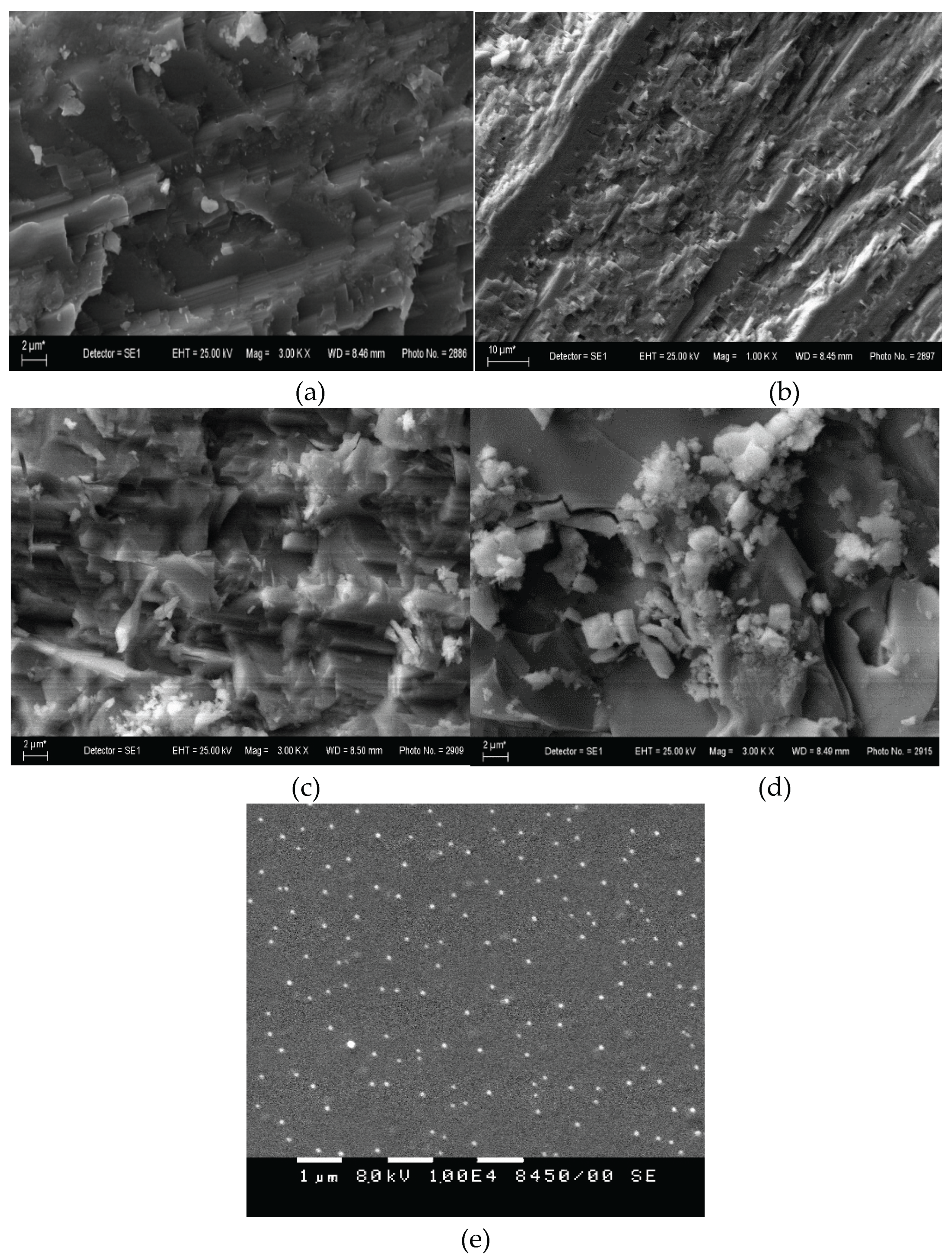
Figure 5 presents the results from the carried-out thermal analysis. The DSC curve for sample Ge14Te81Cu5 shows glass transition temperature (Tg) at 139°C. With increasing the Cu content, Tg decreases and takes a value of Tg = 121°C for Ge13Te77Cu10 and Tg=114°C for Ge12Te73Cu15 and Ge11Te69Cu20. The thermogram of the sample containing 5 mol % Cu shows an exothermic peak at 229°C, which corresponds to the crystallization temperature (Tc) of the material. For the sample dopped with 10 mol % Cu, Tc = 206°C as the observed exothermic peak is more clearly expressed compared to this one obtained for sample Ge14Te81Cu5. On the thermogram for samples Ge12Te73Cu15 and Ge11Te69Cu20 such peak is not to observed. The DSC curve for sample Ge14Te81Cu5 shows a clearly expressed endothermic peak corresponding to melting temperature (Tm) at 369°C. The shoulder at 387°C indicates the presence of two crystalline phases, the first one being in higher concentration. Based on the obtained XRD data, it could be assumed that the peak at 369°C correspondents to tellurium and the shoulder at 387°C to Cu2GeTe3 crystalline phase. The DSC curves for the samples containing 10 mol % and 15 mol % Cu show a doble melting peak, with two clearly expressed maxima, respectively at 369°C and 381°C for Ge13Te77Cu10, and at 369°C and 377°C for Ge12Te73Cu15, which could be associated with the presence of tellurium and Cu2GeTe3 crystalline phases in the material. The thermogram of sample Ge11Te69Cu20 shows an endothermic peak corresponding to melting temperature at 344°C and a shoulder at 363°C indicating the presence of two crystalline phases. Based on the obtained XRD data, we assume that these phases are Te and CuTe.
In Table 2 are presented the obtained values for the density, compactness, molar volume and free volume percentage of all the samples studied, and their dependence on the copper concentration are shown on Figure 6. As seen, the value of the density increases as the copper content increases. Since the size of the Ge and Gu atoms is close (atomic radii of 1.22 and 1,28 Å respectively), the observed increase in the density is probably due to the lowering in the tellurium content as the tellurium atom possess bigger atomic radii of 1.40 Å. The introduction of smaller atoms leads to formation of more dense structure as confirmed by other studies [30]. The dependence of the compactness on the copper concentration follows the same trend as the density, an increase with increasing the Cu content is observed. The increase in the concentration of atoms smaller in atomic radius and less heavy in weight (the atomic weight of Ge, Te and Cu is respectively 72.6 g.mol-1, 127.7 g.mol-1 and 63.5 g.mol-1) leads to the formation of more compact and dense packaged structure. Figure 6c presents the molar volume of the materials as a function of the composition, and it is seen that Vm decreases with the addition of Cu. The observed reduction in the values can be viewed as defined by the following two facts: decrease in the molecular weight and increase in the density of the material. From Figure 6d it is seen, that the free volume percentage has a lowest value for the sample containing 20 mol% copper and highest value for the sample doped with 5 mol% Cu.
The functional relation between the studied physico-chemical futures and the copper content shows similar trend of the curves, namely they increase or decrease with increasing the Cu concentration but not linearly. At around 10 mol % copper content there is a change in the slope of the curve. As explained by many authors [30], this non-linearity is probably due to structural transformation associated with tight bonding, shorter bond length and followed by sharp decrease of the volume.
In Figure 7 (a) are presented the results from measuring the kinetics of birefringence induced in the samples studied at 444 nm recording wavelength of the pump laser.
For the pure PAZO polymer film, the maximal induced birefringence has a value of Δnmax= 0.083. For the layer-by-layer structure an increase in the maximal induced birefringence, respectively Δnmax=0.095, has been measured.
4. Discussion
Generally, the observed higher value of the Δnmax for the bilayer structure based on the azo polymer and Ge14Te81Cu5 in comparison to the pure PAZO film could be viewed as result from: changes in the free volume and/or increased number of scattering and reflectance points within the top layer due to the underlying film morphology (i); interference effects between light reflected at the boundaries between the two layers (ii) and/or some photoinduced phenomena appear in the chalcogenide film contributing to the value of the measured birefringence (iii). Considering (i), a polymer layer spin-coated onto a chalcogenide film closely replicates the surface texture of the underlying film [31,32]. As shown on Figure 4e, there are a lot of grains on the surface of the chalcogenide film, which “copied” into the structure of the azo polymer layer increase the path length of the light within the film and provide opportunity for interaction of the photons with the azo chromophores at various angles. In such case, the Ge14Te81Cu5 film plays a role similar to that of the nano-particles used as dopant in PAZO polymer based composite materials, which according the main reported up to date hypothesis consists in increasing the free volume around the azo chromophores making the number of molecules capable for isomerization higher or in increasing the scattering inside the composite allowing excitation and reorientation of originally off-plane chromophores that would otherwise not contribute to the birefringence [33]. Considering (ii), when light interacts with a layer-by-layer structure, reflections or scatterings from the interface between the two layers can undergo constructive interference resulting in increased light intensity and since in enhanced birefringence of the top layer. Furthermore, scattering and reflectance effects may alter the polarization stay of the incident light. These changes can lead to activation of azo chromophores, even those that are not inherently sensitive to the polarization of the incident light. Considering (iii), the photo-induced phenomena in chalcogenide materials upon irradiation with laniary polarized light are numerous, with different mechanism [34,35]. They are generally stronger in amorphous chalcogenides due to the more space for atomic movement (higher free volume) than in crystalline ones [36] and depend heavily on sufficient light intensity. By the studied bilayer structure, when the light enters the top layer, its intensity dramatically decreases before reaching the chalcogenide layer below as a result from the strong absorption of the azo chromophores at the used wavelength of the laser beam. Since the SEM image of the Ge14Te81Cu5 film suggests, even if is not confirmed, some polycrystallinity, and valuable photoinduced phenomena in chalcogenides require sufficient light intensity to occur, we believe on this stage of our investigation, that the observed higher value of the Δnmax for the bilayer structure in comparison to the pure PAZO film is more due to (i) or (ii). These assumptions are under consideration in our ongoing investigations.
5. Conclusions
New chalcogenides from the system (GeTe6)1-xCux, where x=5, 10, 15 и 20 mol %, has successfully been synthesized by one-step melt quenching technique. The obtained bulk materials consist of GeTe4 and CuTe4 tetrahedral structural units and Te-Te chains. With increasing the copper content, the glass transition temperature decreases from 139°C to 114°C as the crystallization temperature follows the same trend. The carried-out DSC analysis indicate also the presence of two crystalline phases in the bulk materials dopped with 5, 10 and 15 mol% Cu, namely Те и Cu2GeTe3, and the presence of Те и CuTe crystal phases in the sample dopped with 20 mol% Cu. The study of some physicochemical features of the new chalcogenides has shown the existence of a local extremum at 10 and 15 mol% Cu in the functional dependence of the density, compactness, molar volume and free volume on the copper concentration. The most flexible structure possesses sample Ge14Te81Cu5. A layered thin film material based on the synthesized new Ge14Te81Cu5 chalcogenide and the azo polymer PAZO has been fabricated, and the kinetic of the photoinduced birefringence at 444 nm has been measured. The results indicate an increase in the maximal induced birefringence for the layered structure (Δnmax=0.095) in comparison to the non-doped azo polymer film (Δnmax=0.083).
Author Contributions
Conceptualization, Y.T.; D.D and A.S.; methodology, Y.T.; D.D. and A.S.; validation, D.N. and L.N.; investigation, Y.T.; D.D.; V.L. and G.M.; data curation, Y.T.; D.D.; V.V. and G.M.; writing—original draft preparation, A.S. and Y.T.; writing—review and editing, D.N.; L.N.; Y.T.; supervision, D.N.; L.N.
Funding
This research was funded by the European Union-NextGeneration EU, through the National Recovery and Resilience Plan of the Republic of Bulgaria, project № BG-RRP-2.004-0002, "BiOrgaMCT".
Data Availability Statement
All data generated or analyzed during this study are included in the published article.
Acknowledgments
The authors gratefully acknowledge the support provided by the European Union-NextGeneration EU, through the National Recovery and Resilience Plan of the Republic of Bulgaria, project № BG-RRP-2.004-0002, "BiOrgaMCT". Research equipment of Distributed Research Infrastructure INFRAMAT, part of Bulgarian National Roadmap for Research Infrastructures, supported by Bulgarian Ministry of Education and Science was used in this investigation. G. Mateev and D. Nazarova are grateful for the funding from the Bulgarian National Science Fund (BNSF) through project КП-06-Н88/2.
Conflicts of Interest
The authors declare no conflict of interest. The funders had no role in the design of the study; in the collection, analyses, or interpretation of data; in the writing of the manuscript; or in the decision to publish the results.
References
- Zhao, Z.; Clima, S.; Garbin, D.; Degraeve, R.; Pourtois, G.; Song, Z.; Zhu, M. Chalcogenide Ovonic Threshold Switching Selector. Nanomicro Lett. 2024, 11, 16–81. [Google Scholar] [CrossRef] [PubMed]
- Ohta, T.; Ovshinsky, S. R. ; Phase-Change Optical Storage Media. Photo-Induced Metastability in Amorphous Semiconductors; Kolobov A.V.; 1st ed.; Wiley-VCH, Weinheim, Germany, 2003; pp. 310–326.
- Wuttig, M.; Yamada, N. Erratum: Phase-change materials for rewriteable data storage. Nat. Mater. 2007, 6, 1004–1004. [Google Scholar] [CrossRef]
- Fazio, A. Advanced technology and systems of cross point memory. International Electron Devices Meeting (IEDM), San Francisco, CA, USA, 2020, 24.1.1–24.1.4.
- Yamada, N.; Ohno, E.; Akahira, N.; Nishiuchi, K.; Nagata, K.; Takao, M. High Speed Overwritable Phase Change Optical Disk Material, Jpn. J. Appl. Phys. 1987, 26, 61–66. [Google Scholar] [CrossRef]
- Iwasaki, H.; Harigaya, M.; Nonoyama, O.; Kageyama, Y.; Takahashi, M.; Yamada, K.; Deguchi, H.; Ide, Y. Completely Erasable Phase Change Optical Disc II: Application of Ag-In-Sb-Te Mixed-Phase System for Rewritable Compact Disc Compatible with CD-Velocity and Double CD-Velocity. Jpn. J. Appl. Phys. 1993, 32, 5241. [Google Scholar] [CrossRef]
- Fattorini; A. D.; Chèze, C.; García, I. L.; Petrucci, C.; Bertelli, M.; Riva, F. R.; Prili S.; Privitera S. M. S.; Buscema M.; Sciuto, A.; Franco, S.; D'Arrigo G.; Longo, M.; Simone, S.; Mussi, V.; Placidi, E.; Cyrille, M-C.; Tran, N-P.; Calarco, R.; Arciprete, F. Growth, electronic and electrical characterization of Ge-rich Ge–Sb–Te alloy. Nanomater. 2022, 13.
- Petroni, E.; Allegra, M.; Baldo, M.; Laurin, L.; Andrea, S.; Favennec, L.; Desvoivres, L.; Sandrini, J.; Boccaccio, C.; Le-Friec, Y.; Ostrovsky, A.; Gouraud, P.; Bonnevialle, A.; Ranica, R.; Redaelli, A. Study of Ge-Rich Ge–Sb–Te device-dependent segregation for industrial grade embedded phase-change memory. PSS RRL, 2024, 18.
- Zhou, X.; Zhou, X.; Xia, M.; Rao, F.; Wu, L.; Li, X.; Song, Z.; Feng, S.; Sun, H. Understanding phase-change behaviors of carbon-doped Ge2 Sb2 Te5 for phase-change memory application. Appl. Mater. Interfaces 2014, 6, 14207–14214. [Google Scholar] [CrossRef]
- Golovchak, R.; Plummer, J.; Kovalskiy, A.; Holovchak, Y.; Ignatova, T.; Trofe, A.; Mahlovanyi, B.; Cebulski, J.; Krzeminski, P.; Shpotyuk, Y.; Boussard-Pledel, C.; Bureau, B. Phase-change materials based on amorphous equichalcogenides. Sci Rep 2023, 13. [Google Scholar] [CrossRef]
- Malhotra, L. K.; Sripathi, Y.; Reddy G., B. Material science aspects of phase change optical recording. Bull. Mater. Sci., 1995, 18, 725–739. [Google Scholar] [CrossRef]
- Wang, G.; Shen, X.; Nie, Q.; Chen, F.; Wang, X.; Fu, J.; Chen, Y.; Xu, T.; Dai, S.; Zhang, W.; Wang, R. Te-based chalcogenide films with high thermal stability for phase change memory. J. Appl. Phys. 2012, 111, 093514–1. [Google Scholar] [CrossRef]
- Saito, Y.; Koike, J. Optical contrast and laser-induced phase transition in GeCu2Te3 thin film. Appl. Phys. Lett. 2013, 102. [Google Scholar] [CrossRef]
- Dongol, M.; AbouZied, M.; Gamal, G.A.; El-Denglawey, A. Synthesis and the RDF fine structure of Ge0. 15Te0.78Cu0.07 bulk alloy. Optik, 2016, 127, 8186–8193. [Google Scholar]
- Skelton, J. M.; Kobayashi, K.; Sutou, Y.; Elliott, S. R. Origin of the unusual reflectance and density contrasts in the phase-change material Cu2GeTe3. Appl. Phys. Lett. 2013, 102, 224105. [Google Scholar] [CrossRef]
- Saito, Y.; Sutou, Y.; Koike, J. Phase change characteristics in GeTe-CuTe pseudobinary alloy films. J. Phys. Chem. C 2014, 118, 26973–26980. [Google Scholar] [CrossRef]
- Saito, Y.; Sutou, Y.; Fons, P.; Shindo, S.; Kozina, X.; Skelton, J. M.; Kolobov, A.V.; Kobayashi, K. ; Electronic Structure of Transition-Metal Based Cu2GeTe3 Phase Change Material: Revealing the Key Role of Cu d Electrons. Chem. Mater. 2017, 29, 7440–7449. [Google Scholar] [CrossRef]
- W. Ming; Chen L.; The microstructure and electrical and optical properties of Ge–Cu–Te phase-change thin films. Cryst Eng Comm, 2024, 26, 395–405.
- Mishra, S. P.; Krishnamoorthy, K.; Sahoo, R.; Kumar, A. Organic–inorganic hybrid polymers containing 3,4-ethylenedioxythiophene and chalcogens in the main chain. J. Mater. Chem. 2006, 16, 3297–3304. [Google Scholar] [CrossRef]
- Gerbreders, A.; Teteris, J.; Kolobjonoks, V. Holographic recording in polymer composites of organic photochromes and chalcogenides, Sixth International Conference on Advanced Optical Materials and Devices, Riga, Latvia, 12. 11. 2008, 7142. [Google Scholar]
- Bertelli, M.; Sfuncia, G.; De Simone, S.; Fattorini, A. D.; Calvi, S.; Mussi, V.; Arciprete, F.; Mio, A. M.; Calarco, R.; Longo, M. Stable chalcogenide Ge–Sb–Te heterostructures with minimal Ge segregation. Sci Rep, 2024, 14, 15713. [Google Scholar] [CrossRef]
- Berberova-Buhova, N.; Nedelchev, L.; Stoykova, E.; Nazarova, D. Optical response evaluation of azopolymer thin solid films doped with gold nanoparticles with different sizes. J. Chem. Technol. Metall, 2022, 57, 671–675. [Google Scholar]
- Teteris, J.; Gertners, U. Optical field-induced surface relief formation on chalcogenide and azo-benzene polymer films, International Conference on Functional Materials and Nanotechnologies, Riga, Latvia, 17–20 April.
- Nazarova, D.; Nedelchev, L.; Sharlandjev, P.; Dragostinova, V. Anisotropic hybrid organic/inorganic (azopolymer/SiO2 NP) materials with enhanced photoinduced birefringence. Appl. Opt. 2013, 52, E28–E33. [Google Scholar] [CrossRef]
- Mateev, G.; Nazarova, D.; Nedelchev, L. Increase of the Photoinduced Birefringence in Azopolymer Films Doped with TiO2 Nanoparticles. J. Phys. Technol. 2019, 3, 18–21. [Google Scholar]
- Nazarova, D.; Nedelchev, L.; Stoykova, E.; Blagoeva, B.; Mateev, G.; Karashanova, D.; Georgieva, B.; Kostadinova, D. Photoinduced birefringence in azopolymer doped with Au nanoparticles. J. Phys. Conf. Ser. 2019, 1310, 012018. [Google Scholar] [CrossRef]
- Stoilova, A.; Dimov, D.; Trifonova, Y.; Lilova, V.; Blagoeva, B.; Nazarova, D.; Nedelchev, L. Preparation, structural investigation and optical properties determination of composite films based on PAZO polymer doped with GeTe4-Cu chalcogenide particles. Eur. Phys. J. Appl. Phys. 2021, 95, 30301. [Google Scholar] [CrossRef]
- Nikolova, L.; Ramanujam, P.S. Polarization Holography; Cambridge University Press: Cambridge, UK, 2009. [Google Scholar]
- Delgado, G.; Mora, A.; Pirela, M. Velásquez-Velásquez, A. ; Villarreal, M.; Fernández, B. Structural refinement of the ternary chalcogenide compound Cu2GeTe3 by X-ray powder diffraction. Phys. Stat. Sol. (a), 2004, 201, 2900. [Google Scholar]
- Petkov, P.; Ilchev, P.; Ilcheva, V.; Petkova, T. ; Physico-chemical properties of Ge-Te-Ga glasses. J. Optoelectron. Adv. M. 2007, 9, 3093–3096. [Google Scholar]
- Tyona, M. D. A comprehensive study of spin coating as a thin film deposition technique and spin coating equipment, Adv. Mater. Res. 2013, 2, 181–193. [Google Scholar]
- Jemelka, J.; Palka, K.; Janicek, P.; Slang, S.; Jancalek, J.; Kurka, M.; Vlcek, M. Solution processed multi-layered thin films of Ge20Sb5S75 and Ge20Sb5Se75 chalcogenide glasses. Sci Rep, 2023, 13, 16609. [Google Scholar] [CrossRef]
- Nazarova, D.; Nedelchev, L.; Berberova-Buhova, N.; Mateev, G. Nanocomposite photoanisotropic materials for applications in polarization holography and photonics. Nanomaterials, 2023, 13, 2946. [Google Scholar] [CrossRef]
- Krecmer, P.; Moulin, A. M.; Stephenson, R. J.; Rayment, T.; Welland, M. E.; Elliott S., R. Reversible Nanocontraction and Dilatation in a Solid Induced by Polarized Light. Sci. 1997, 277, 1799–1802. [Google Scholar] [CrossRef]
- Tanaka, Ke.; Gotoh, T.; Nakayama, H. Anisotropic patterns formed in Ag–As–S ion-conducting amorphous semiconductor films by polarized light. Appl. Phys. Lett. 1999, 75, 2256–2258. [Google Scholar] [CrossRef]
- Popescu, M. Disordered chalcogenide optoelectronic. J. Optoelectron. Adv. M. 2005, 7, 2189–2210. [Google Scholar]
Figure 1.
XRD patterns of the samples from the system GeTe6-Cu.
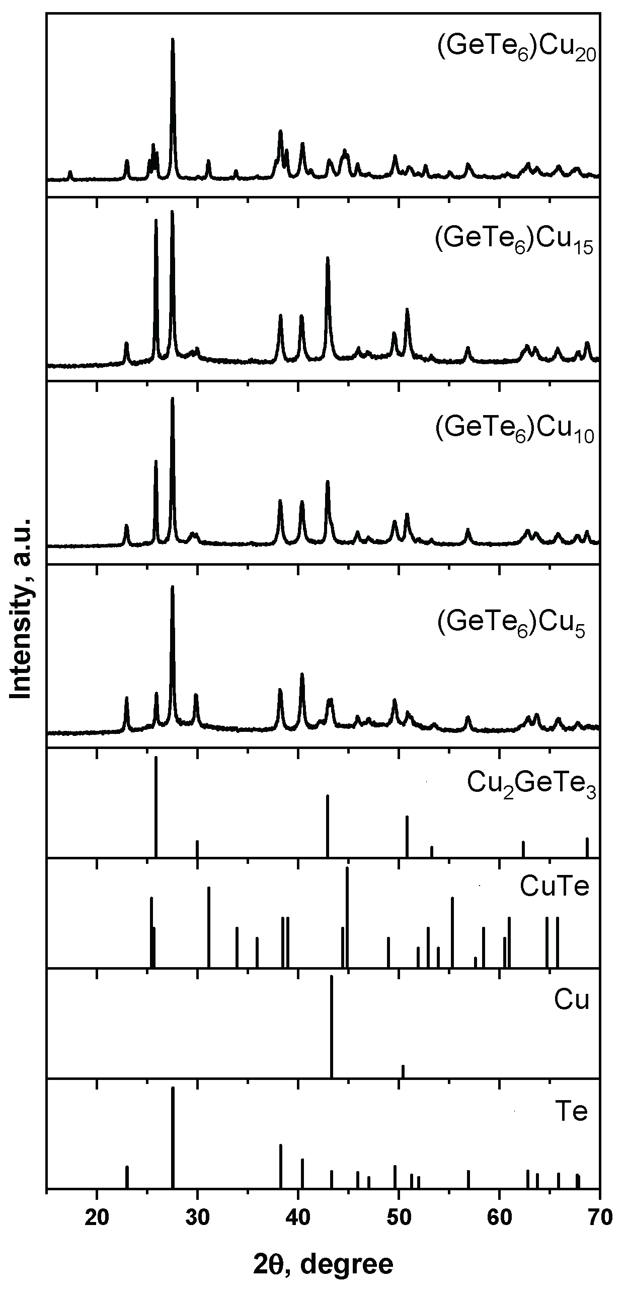
Figure 2.
Energy-dispersive spectrum of sample Ge14Te81Cu5.
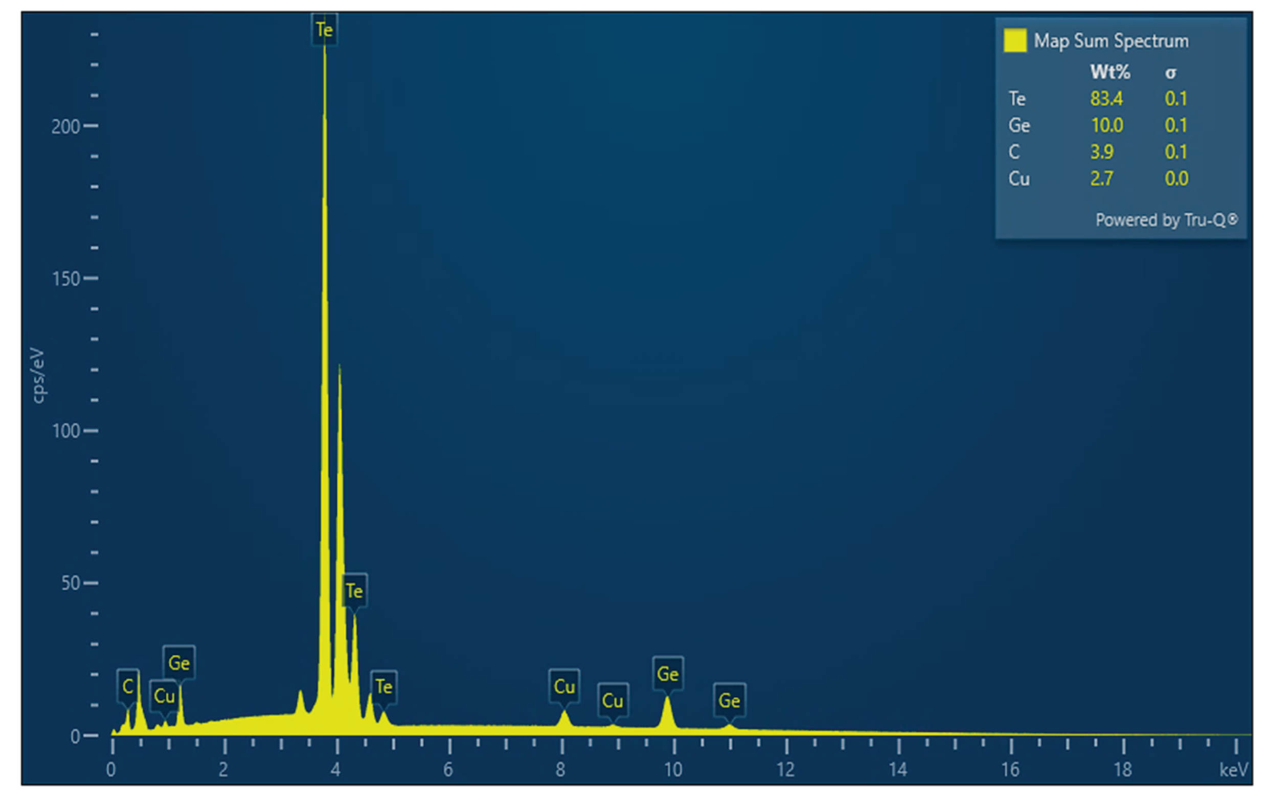
Figure 5.
DSC curves of the samples studied.
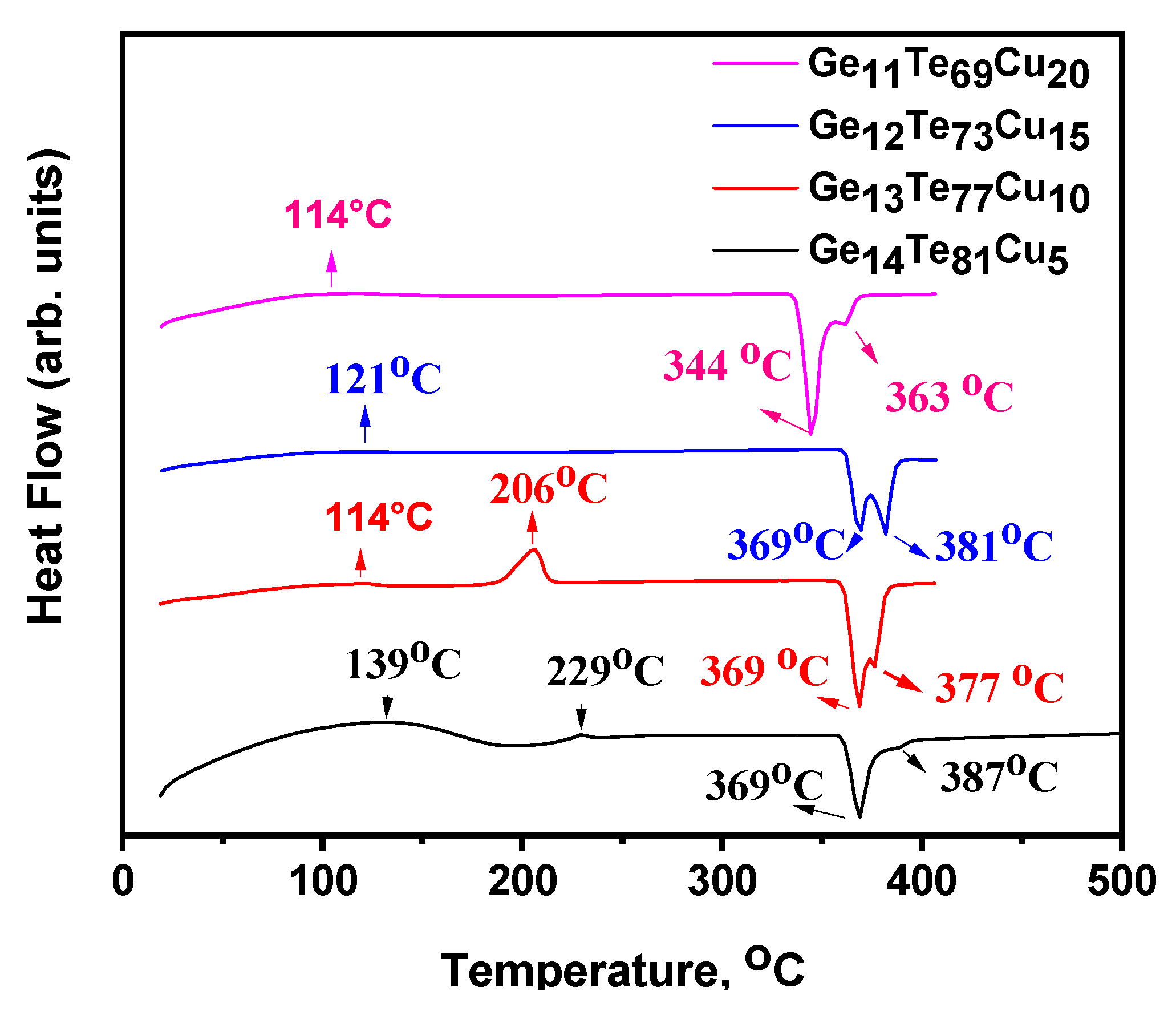
Figure 6.
Density (a), compactness (b), molar volume (c) and FVP (d) dependence on the composition.
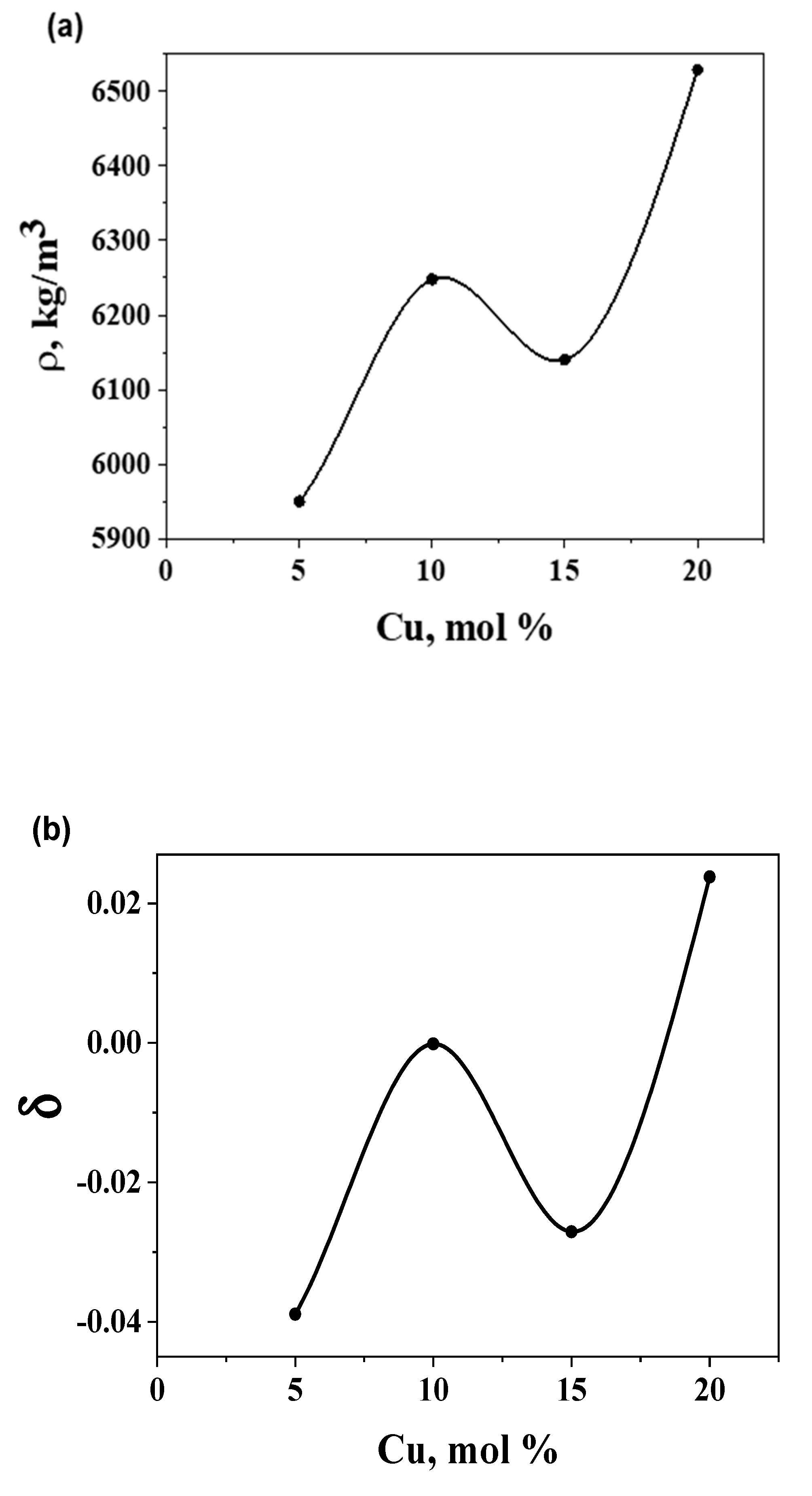
Figure 7.
Birefringence kinetics for the samples studied induced at 444 nm.
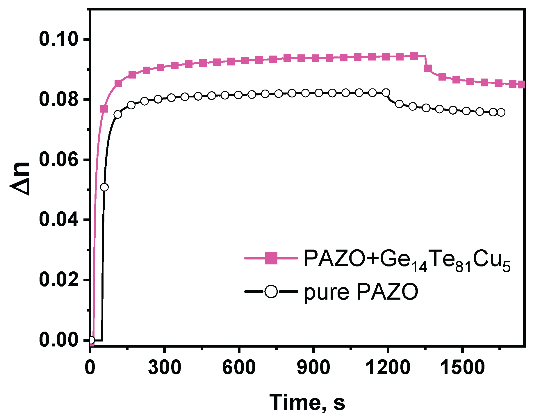

Table 1.
EDS elemental analysis (expressed in percentage of weight) and comparison with the calculated elemental concentration in mol % converted to weight percent (wt. %).
Table 1.
EDS elemental analysis (expressed in percentage of weight) and comparison with the calculated elemental concentration in mol % converted to weight percent (wt. %).
| Sample mol % |
Theoretically determined elemental concentration, wt. % | Elemental concentration determined by EDS, wt. % |
|---|---|---|
| Ge14Te81Cu5 |
Ge – 8.7 Te – 88.6 Cu – 2.7 |
Ge – 10.0±0.1 Te – 83.4±0.1 Cu – 2.7±0.0 |
| Ge13Te77Cu10 |
Ge – 8.3 Te – 86.1 Cu – 5.6 |
Ge – 6.6±0.1 Te – 82.2±0.1 Cu – 5.6±0.0 |
| Ge12Te73Cu15 |
Ge – 7.8 Te – 83.6 Cu – 8.6 |
Ge – 7.9±0.1 Te – 76.5±0.1 Cu – 9.7±0.0 |
| Ge11Te69Cu20 |
Ge – 7.3 Te – 81.0 Cu – 11.7 |
Ge – 0.7±0.0 Te – 71.3±0.1 Cu – 9.2±0.0 |
Table 2.
Physico-chemical properties of the bulk samples studied.
| Sample |
Density, 103 kg/m3 |
Compactness, 10-2 |
Molar volume, 10-5m3/mol |
FVP, % |
|---|---|---|---|---|
| Ge14Te81Cu5 | 5.950 | -3.890 | 1.961 | 4.00 |
| Ge13Te77Cu10 | 6.248 | -0.015 | 1.825 | 0.12 |
| Ge12Te73Cu15 | 6.140 | -2.709 | 1.814 | 2.80 |
| Ge11Te69Cu20 | 6.529 | 2.378 | 1.666 | -2.28 |
Disclaimer/Publisher’s Note: The statements, opinions and data contained in all publications are solely those of the individual author(s) and contributor(s) and not of MDPI and/or the editor(s). MDPI and/or the editor(s) disclaim responsibility for any injury to people or property resulting from any ideas, methods, instructions or products referred to in the content. |
© 2025 by the authors. Licensee MDPI, Basel, Switzerland. This article is an open access article distributed under the terms and conditions of the Creative Commons Attribution (CC BY) license (http://creativecommons.org/licenses/by/4.0/).
Copyright: This open access article is published under a Creative Commons CC BY 4.0 license, which permit the free download, distribution, and reuse, provided that the author and preprint are cited in any reuse.


