Submitted:
21 June 2025
Posted:
24 June 2025
You are already at the latest version
Abstract
Silver nanowires (AgNWs)-based transparent conductive films are critical for flexible electronics due to their excellent optoelectronic properties and mechanical flexibility. We discussed the preparation methods of AgNWs films, including Mayer rod coating, spray coating, spin coating, screen printing, and inkjet printing, and analyzed their advantages, limitations, and applicable scenarios. Furthermore, we systematically explored anti-oxidation strategies for AgNWs, such as surface modification, composite structure design, and process optimization. Potential approaches to enhance the conductivity, transparency, and flexibility of AgNWs films were also outlined. Finally, we discussed future applications and challenges, offering insights for the development of next-generation flexible transparent electrodes.
Keywords:
silver nanowires films
; transparent conductive properties
; preparation technology
; antioxidation
; research progress
1. Introduction
With the rapid development of flexible electronic devices, the demand for flexible transparent conductive thin films (TCFs) has been increasing in the past two decades. It is known that TCFs are widely used in foldable smartphones [1], wearable devices [2], organic light-emitting diodes [3], organic solar cells (OSCs) [4], flexible sensors [5], electromagnetic shielding [6] and so on. The most commonly used TCF material, indium tin oxide (ITO), which belongs to a transparent conductive oxide (TCO), possesses outstanding electrical and optical performance, including relatively low resistivity and high visible transmittance. However, due to the scarcity and high cost of metal indium, as well as the tendency of ITO to crack under bending stress, the application of ITO in flexible devices is limited. Unfortunately, other TCO materials also have the disadvantage of poor bendability.
In recent years, other flexible transparent conductive materials, including conductive polymers, carbon nanotubes (CNTs), graphene, and silver nanowires (AgNWs), have attracted widespread attention. Conductive polymers have attracted significant attention due to their solution processability and flexibility. However, their structures are prone to damage, which may lead to the loss of electrical conductivity [7]. Due to the difficulty in the large-scale preparation of uniform and high-quality films, CNTs have not yet been widely applied [8]. Graphene is known for its exceptional electrical, mechanical, and optical properties. However, the preparation of graphene mainly relies on methods such as chemical vapor deposition, which requires high temperature, high pressure, large equipment investment, and high operating costs [9]. In addition, the large-scale production of graphene also faces technical challenges. For example, due to the easy stacking between graphene layers, their electrical performance will significantly decrease.
As is well known, metallic silver has the highest conductivity, and AgNW can achieve uniform dispersion on various substrates and construct effective networks, resulting in AgNW thin films with high transparency and good conductivity [10]. It has enormous potential for applications in fields such as flexible displays, large-area solar cells, smart touch panels, and wearable electronic devices. This paper reviews the characteristics, preparation methods, application fields, challenges, and prospects of transparent conductive AgNW thin films, which may offer a reference for the research and application of promising flexible TCFs.
2. Characteristics of Flexible Transparent Conductive Films
2.1. Transparency and Conductivity
The implementation mechanism of transparency and conductivity of AgNW is different from TCO. AgNW is formed by a sparse conductive network of high aspect ratio nanowires (> 1000), thereby achieving continuous conductive paths and high transmittance at low packing density. The unique advantage of AgNWs lies in the high percolation threshold brought by their high aspect ratio. Guo et al. [11] achieved a visible transmittance of 92.2% and a sheet resistance of 12.9 Ω/sq at a network density as low as 0.1 mg/cm² through the multi-layer-oriented arrangement of AgNWs. Tao et al. [12] further pointed out that high visible transmittance of ~80% and low resistance of ~75 Ω/sq can be maintained simultaneously with haze < 2% by controlling the diameter of AgNWs (< 50 nm) and aspect ratio (> 2000), which is difficult to achieve with traditional materials such as ITO. Chen et al. [13] successfully prepared large-area (70 × 15 cm2) stretchable ordered AgNW electrodes. They utilized ionic liquid induction and ultra-wet transfer techniques to achieve a large-scale ordered arrangement of AgNWs, and further improved their performance through chemical welding techniques. Zhang et al. [14] embedded AgNWs microgrids into polydimethylsiloxane (PDMS) to prepare stretchable transparent conductive electrodes (TCEs), which were then used to fabricate polymer dispersed liquid crystal (PDLC) devices with optical modulation, stretchability, and pressure sensing functions. The embedded design reduces the thin layer resistance of the electrode to 19.88 Ω/sq and achieves a transparency of 85%. At 100% strain, the resistance only increased by 1.36 times. After 1000 bending cycles at a 5 mm radius, the resistance fluctuation is less than 20%.
2.2. Flexibility and Stability
The stability of the optoelectronic properties of flexible TCFs is closely related to the number of bending or stretching cycles. Tang et al. [15] prepared the AgNWs/ super-flexible transparent wood (STW) composite electrode via Meyer rod coating. The 91.4% visible transmittance after 1500 bending cycles at a 2 mm radius can be maintained, which is attributed to the "sliding-rearrangement" mechanism of the nanowire network rather than rigid fracture. However, due to stress concentration during the bending process, high-density networks with tightly overlapping nanowires are prone to fracture. Therefore, interface polymer coatings are needed to enhance mechanical compatibility. Hao et al. [16] prepared electrochromic electrodes using stretchable AgNW/PT-PDMS composite materials. It is worth noting that the electrode maintained excellent electrochromic performance after 10000 bending cycles or 500 stretching cycles. Wang et al. [17] prepared stretchable AgNW/Pat PDMS conductive films on PDMS substrates using the rod coating method. Subsequently, the film was applied to the manufacturing of stretchable strain sensors. The results not only demonstrated the excellent flexibility of AgNW/Pat PDMS conductive film but also verified its high stability. Kim et al. [18] inserted polyurethane urea between AgNWs and PDMS to enhance the interfacial adhesion between AgNWs and PDMS. The AgNW film maintains the stability and reversibility of its optoelectronic properties after 100 cycles of 50% stretching. These findings indicate that this newly developed electrode has potential for direct integration into various high-performance flexible electronic devices.
3. Preparation Methods of AgNW-based Transparent Conductive Films
The main preparation methods of AgNW-based transparent conductive films include liquid-phase chemical reduction, template method, and electrochemical method.
For large-scale preparation of discrete AgNW dispersions, liquid-phase chemical reduction (especially the polyol method) is the most preferred and mature technical route at present. Polyvinylpyrrolidone (PVP) is used as a structure directing agent and polyol as a solvent and a mild reducing agent at the same time to selectively adsorb on the specific crystal plane (usually {100} plane) of silver crystal, inhibit the growth of this plane, promote the preferred growth of silver atoms along the<111>direction, form a linear structure, and accurately adjust the synthesis parameters (such as reaction temperature, molecular weight of PVP, NaBr concentration, etc.) to achieve the balance of conductivity and transmittance of TCFs [19]. Because PVP residue may affect the subsequent application performance, Ge et al. [20] proposed a rapid electrochemical cleaning strategy to completely remove the polyvinylpyrrolidone (PVP) ligand on the surface of AgNWs and significantly improve the in-plane and out-of-plane carrier transport performance of AgNW films. After cleaning, the square resistance of the film decreased from 49 Ω/sq to 13 Ω/sq (the transmittance at 550 nm was 90.91%), and the interface resistance decreased by 94.3%.
The anodic aluminum oxide (AAO) template is the most widely used template in the preparation of AgNWs. It can obtain ordered nanopore arrays through electrochemical anodic aluminum oxide sheets. AgNW arrays with uniform diameter and ordered arrangement can be obtained by electrodeposition or chemical deposition of silver in the pores, and finally dissolving the AAO template with NaOH or H₃PO₄, and the length and diameter can be accurately controlled by the template [21].
The electrochemical method is suitable for the growth of nanowire structures directly on the target substrate. In the electrolyte containing silver ions (such as AgNO₃), AgNWs were reduced and deposited on the cathode by applying current. Yorick et al. [22] proposed a bottom-up electrochemical growth method and prepared a high aspect ratio AgNW grid transparent electrode by substrate conformal imprint lithography combined with electrochemical deposition. The obtained electrode has high transmittance (95.9%) and low sheet resistance (3.7 Ω/sq), which breaks through the trade-off between transmittance and resistance of traditional transparent electrodes, and the process can be extended to large-area preparation. At present, the preparation processes of transparent conductive films based on AgNWs mainly include Meyer Rod Coating, Spraying, Spin Coating, Silk-screen Printing, Inkjet Printing, etc.
3.1. Meyer Rod Coating Method
The Meyer rod coating method is a relatively simple thin film preparation process, and its basic method is as follows. Drop the AgNW dispersion onto the polymer substrate, and then use a Meyer rod to evenly spread the solution into a thin film, as shown in Figure 1. The thickness of the membrane is determined by the concentration of Meyer rods and dispersion solutions of different specifications. Due to the advantages of good uniformity and low cost of the materials used in this coating method, it is one of the popular coating methods in the current market.
Guo et al. [11] developed a conductive ink based on AgNWs aqueous solution and hydroxypropyl methylcellulose (HPMC) and used Meyer rod coating technology to realize the directional arrangement of AgNWs. Through this method, they prepared multilayer cross-linked AgNWs/HPMC composite films. The transmittance of the films in the visible light region was 92.2%, and the sheet resistance was 12.9 Ω/sq. This method achieved the collaborative optimization of "structure performance" through the directional arrangement induced by fluid mechanics, which had both high performance and process simplicity, and better coordinated the contradiction between uniformity and large-scale production in the traditional method. Tang et al. [15] used Meyer rod coating technology to deposit AgNW on STW substrates to prepare flexible electrodes. Even after 1500 bending cycles at a 2 mm radius, the electrode maintained a high transmittance of 91.4% in the visible light region, and the sheet resistance was 52 Ω/sq. Zhang et al. [24] prepared an AgNW film by the Meyer rod coating method and creatively used a xenon lamp to dynamically move at a speed of 0.05 m/s for heating and curing. The AgNW film prepared by this method has high uniformity, low sheet resistance (about 24 Ω/sq), and high visible light transmittance (about 91%). The dynamic movement of xenon lamps ensures uniform temperature distribution and effectively reduces the agglomeration of AgNWs. Compared with natural drying (uniformity factor 0.3415) and static heating (uniformity factor 0.5167), the uniformity of the film prepared by the dynamic heating method is significantly improved, and its uniformity factor reaches 0.2915.
3.2. Spraying Method
The spraying technique is compatible with a wide range of substrate materials and enables efficient, large-area film production. Furthermore, films with varying thicknesses can be fabricated by adjusting the spraying duration, the concentration of the dispersion liquid, and the number of spraying cycles according to specific requirements. Low material efficiency due to significant material loss during the spinning process, and challenges in coating large-area or irregularly shaped substrates [25]. This preparation method involves the direct deposition of the AgNWs dispersion liquid onto the entire substrate to form a film, as depicted in Figure 2.
Crêpellière et al. [26] deposited AgNWs on the preheated glass substrate by spraying technology. After spraying for 3 minutes, uniform coverage was achieved on an area of 100 cm2, forming a dense conductive network. The performance parameters of the obtained AgNW networks are: block resistance 9 Ω/sq, visible light transmittance 91.7%, and haze factor 3.7%. At the same performance level, their coverage area (100 cm2) is superior to most small-area preparation methods reported in the literature. Gholami et al. [27] prepared the composite film of polystyrene (PS) embedded in AgNWs by a spray deposition method, and further coated the gold layer on the surface of AgNWs by the double pulse electrodeposition method, PS-AgNW@Au Composite electrode. The test results show that the square resistance of the composite electrode is 24 Ω/sq, and the transmittance in the visible light region is 84%. In the repeated bending test with a 4 mm radius, the resistance increases by only 22% after 2000 bends. The composite structure has excellent chemical stability, high conductivity, good light transmittance, and outstanding flexibility. Zheng et al. [28] developed a straightforward spray-assisted method to achieve an ordered arrangement of AgNWs. Compared to conventional AgNW electrodes, the ordered arrangement electrode showed significant enhancements, with the former achieving a visible light transmittance of 86.6% and a sheet resistance of 18.3 Ω/sq, whereas the latter exhibited a light transmittance of 85% and a sheet resistance of 63 Ω/sq. Electrochemical impedance spectroscopy (EIS) confirmed that the optimization of electrode conductivity is the key. The orderly arrangement forms an efficient conductive network by reducing the percolation threshold, which provides an electrode solution with low resistance and high permeability for electrochromic devices.
3.3. Spin Coating Method
The spin coating process involves key steps to ensure a uniform film. Initially, the AgNW dispersion is applied to the substrate, which is then secured on a high-speed rotating turntable. The centrifugal force from the spinning spreads the liquid evenly, resulting in a consistent film. This efficient method is widely used for thin film production across industries. The film-forming uniformity is relatively low, the thickness control accuracy is poor, and it may cause uneven spray particles or an orange peel effect [25].
Song et al. [29] prepared innovative WOx/AgNWs FTCFs on flexible polyethylene naphthalate (PEN) substrate by the solution method and spin coating process. The key to the film is the introduction of an ultra-thin WOx layer, which can effectively inhibit the oxidation of AgNWs by physically wrapping AgNW networks and significantly enhance the mechanical flexibility and adhesion of the film to the pen substrate. Thanks to the multiple protection and enhancement of the WOx layer, the composite film shows excellent comprehensive properties: not only has a block resistance as low as 9.4 Ω/sq and an optical transmittance as high as 82.6% but also shows excellent mechanical stability (resistance change is less than 10% after 1000 bending times at a radius of 5 mm or strip stripping test) and environmental stability (stable under high temperature, high humidity, and strong oxidation conditions). Shi [30] prepared a flexible transparent conductive film on polyethylene terephthalate (PET) substrate by a two-step spin coating method. After 6 layers of spin coating, AgNWs with a diameter of 40 nm achieved a breakthrough in performance: the square resistance was as low as 13 Ω/sq, and the transmittance at 550 nm was 89.7% (haze 4.23%). AgNW diameter has a decisive impact on the performance of conductive networks: under the same area coverage, the smaller diameter (20 nm) forms a denser conductive network, making the square resistance (24.8 Ω/sq) significantly lower than the larger diameter (60 nm, 62.4 Ω/sq). The film exhibits excellent stability (the change rate of square resistance after 1000 bending cycles<10%) and excellent infrared performance. Wang et al. [31] prepared an innovative MXene/AgNWs/graphene sandwich structure hybrid TCFs by spin coating, using MXene as the intermediate layer to enhance adhesion, and graphene as the top layer to protect and fill the AgNW network, improving conductivity, flatness, and stability. The transmittance of the composite film at 550 nm is 87.5%, and the square resistance is 14.4 Ω/sq. The composite film has the advantages of low surface roughness, strong adhesion, and high stability.
3.4. Silk-screen Printing
The screen printing offers an efficient and cost-effective solution for creating films on various substrates. The process involves several key steps: Initially, a screen with a tailored pattern is developed, while AgNWs are blended into a suitable ink. This ink is then applied to the screen, where pressure from a squeegee facilitates the ink's passage through the screen's mesh and onto the substrate, effectively forming an AgNW film. This flexible printing method is ideal for producing complex patterns, making it particularly useful in manufacturing flexible printed circuit boards and flexible thin-film transistors [32][].
Li et al. [33] used screen printing technology (HPMC AgNWs ink/98t mesh template) to prepare a 15 × 20 cm2 large area and high uniformity AgNW transparent conductive film. By adjusting the concentration of AgNWs to optimize the conductive network, the film achieved excellent comprehensive performance: low square resistance (13.0 ± 0.6 Ω/sq), high transmittance (95.3% @ 550 nm), low haze (3.86%), and high flatness (surface roughness 3.33 nm). The film can directly construct a low-voltage-driven transparent heater, showing excellent heating uniformity and long-term stability. Xu et al. [35] proposed a preparation method for AgNWs/graphene oxide (GO) hybrid transparent electrodes based on screen printing: the functional design of the electrode structure was realized by printing AgNWs and GO layers alternately. The electrode has high conductivity (11.9 Ω/sq), high light transmittance (83.5% @ 550 nm), and excellent mechanical flexibility. Its core advantages are derived from the triple protection mechanism of the GO layer: an antioxidant barrier (preventing environmental erosion and maintaining stable performance after thermal oxidation treatment), a mechanical buffer layer (resistance change rate < 5% after 1500 bending cycles), and biological interface isolation (avoiding direct contact between AgNWs and skin to improve biocompatibility). Li et al. [35] successfully prepared films with low square resistance (1.1 ~ 9.2 Ω/sq) and high transmittance (75.2 ~ 92.6%) by accurately controlling the mesh number of the screen (325 mesh) and the thickness of the AgNW ink (10 μm). This process innovatively combines the low-concentration ink formula and flash rapid sintering technology to synchronously achieve high resolution, excellent conductivity, and optical properties in 20 × 20 cm2 large-area printing, which perfectly meets the needs of large-scale manufacturing.
3.5. Inkjet Printing Method
The inkjet printing represents an innovative technology with significant market potential in the domain of large-area flexible and stretchable electronics. This process involves converting conductive film materials into conductive inks, which are then rapidly deposited onto a substrate through specialized nozzles to form a TCF. As illustrated in Figure 3, this method offers several advantages: it enables the creation of complex patterns without the need for etching processes, promotes rapid film formation, and is user-friendly. Additionally, it boasts a high material utilization rate.
Wang et al. [37] developed AgNW inks suitable for inkjet printing and successfully prepared high-performance AgNW-TCFs by inkjet printing on PET substrate. The films have both low square resistance (13 Ω/sq) and high transmittance (81.9%), and their excellent patterning ability and conductive reliability are verified by precision printing of heart-shaped patterns. Wu et al. [38] used inkjet printing technology, innovatively selected AgNWs with a length diameter ratio of 1000, and added modified polysilane lubricant to prepare functional ink. By accurately controlling the equipment temperature and ink concentration (inhibiting the aggregation of AgNWs), AgNW-TCFs with tunable photoelectric properties were successfully prepared: the transmittance reached 83.1% at 550 nm wavelength, and the square resistance was precisely adjusted in the range of 34.0 ~ 78.3 Ω/sq. The film also exhibits excellent mechanical stability - resistance change rate < 2.5% after 1000 bending cycles.
To further investigate the influence of deposition density on the performance of AgNW films, the figure of merit (FOM) was introduced to evaluate the comprehensive performance (transparent conductivity) of the TCF. The commonly adopted model is the ratio of direct current (DC) conductivity σDC to phototransmittance σOp, that is, σDC/σOp, which was taken into consideration [39,40]. This ratio can also be calculated from the sheet resistance and light transmittance using Equation (1).
Z0 represents the impedance of free space, which is a physical constant with a value of 376.7 Ω. Rs represents the sheet resistance, and its unit is Ω/sq. Tav represents light transmittance (%). The higher the FOM value, the better the optoelectronic performance of the FTCFs, indicating good electrical conductivity and high light transmittance.
Based on the data obtained from the above preparation methods of AgNWs and following Equation (1), the calculation results of the FOM of AgNW films prepared by various methods are shown in Table 1.
Table 1 showcases the performance parameters of various thin-film deposition methods, including Tav, Rs, FOM, and references. Meyer Rod Coating demonstrates high Tav (92.2% and 91%) and relatively low Rs (12.9 Ω/sq and 10 Ω/sq), resulting in higher FOM (352.33 and 390.08), indicating favorable transparent-conductiv9 properties. Spraying, with Tav around 84% and Rs of 24 Ω/sq or 12.95 Ω/sq, has lower FOM (86.16 and 165.55), possibly due to film-uniformity issues. Spin Coating, with Tav of 82.6%–87.5% and Rs of 9.4 Ω/sq ~14.4 Ω/sq, yields FOM values of 199.78 and 189.44, balancing conductivity and transmittance. Silk-screen printing stands out with a Tav of 95.3%, Rs of 13.6 Ω/sq, and the highest FOM (568.47), suggesting excellent comprehensive performance. Inkjet Printing exhibits significant variability: Tav of 83.1% and 74%, Rs of 34.0 Ω/sq and 2.9 Ω/sq, leading to FOM of 57.12 and 399.74, highlighting sensitivity to process parameters. Overall, each method has unique strengths and limitations, guiding selections based on application needs for transparency, conductivity, and process control.
From Table 2, in the realm of AgNW film preparation, the process characteristics of different methodologies diverge significantly owing to disparities in their underlying mechanisms. Spin-coating and inkjet printing theoretically enable exceptionally high film uniformity through dynamic solution spreading or precise ink droplet positioning. Nevertheless, the former is constrained by uneven centrifugal force distribution at the edges of large-area substrates, while the latter is susceptible to nozzle clogging and ink rheological properties, necessitating rigorous regulation of operational parameters to achieve practical uniformity. The uniformity of spraying and screen printing hinges directly on equipment precision, with spray stability and screen squeegee pressure uniformity serving as critical control factors, respectively.
In terms of thickness control, spin-coating (via adjustments in rotation speed and solution concentration) and inkjet printing (via the design of ink droplet volume and deposition layers) can both achieve sub-micron-level precision, rendering them suitable for fabricating ultra-thin or multi-layer composite structures. Conversely, screen printing and spraying technologies are better suited for preparing medium-to-thick films due to their process characteristics. The former relies on screen mesh count and paste viscosity, while the latter adjusts film thickness through spray volume and number of passes, meeting the requirements for large-area uniform coatings.
Notable differences also emerge in equipment cost and production efficiency: Meyer rod coating and screen printing entail lower basic equipment costs, with the latter enabling high-speed large-area patterning production when integrated with automated production lines, making it ideal for low-cost industrial mass production. Inkjet printing (particularly industrial-grade high-precision systems) and spraying (automated spraying lines) incur medium-to-high costs. The former is more appropriate for small-area high-precision patterning due to printing speed limitations, while the latter serves as an efficient choice for large-area substrates (e.g., solar cells, architectural glass) under its continuous coating capability.
In summary, spin-coating is the method of choice in laboratory research scenarios due to its advantage in producing high-quality films in small-areas. In industrial applications, the selection diverges based on requirements: screen printing is suitable for large-area patterning production, spraying technology caters to large-area low-cost coating preparation, and inkjet printing demonstrates unique advantages in constructing high-precision complex structures (e.g., flexible electronics, biosensors) through its precise positioning capability. This exemplifies the process adaptation logic from fundamental research to engineering applications.
4. Methods to AgNW Networks Coated with Metal Oxides
AgNW networks, as emerging structures for constructing efficient TCEs, show great potential for future technological development. However, this structure suffers from problems such as insufficient thermal, chemical, and electrical stability. For example, AgNWs are prone to oxidation and agglomeration, and they also have relatively high interfacial contact resistance and need optimization in surface roughness. Coating with metal oxides (MOx) is an important improvement method. This approach can not only enhance the oxidation resistance and thermal stress resistance of AgNW networks, and regulate optical and electrical properties, but also reduce interfacial contact resistance, thereby further optimizing the comprehensive performance of AgNW networks.
The methods for improving the performance of AgNW networks based on metal oxide (MOx) coatings are mainly divided into two categories: physical processes and chemical processes, as shown in Figure 4. The following is a detailed explanation combining the characteristics, advantages, and application scenarios of each process.
4.1. Physical Vapor Deposition Methods
Physical vapor deposition (PVD) methods are widely used for coating AgNW networks with metal oxides. These methods involve the transfer of material in the vapor phase and subsequent deposition onto the AgNW surface, as shown in Figure 4c.
4.1.1. Sputtering Deposition
Sputtering deposition, as an efficient PVD technology, uses high-energy ions to bombard metal oxide targets in the plasma environment to deposit sputtered particles on the surface of AgNW networks, which has three core advantages: high deposition rate, nano thickness control, and excellent coating uniformity. However, this technology needs high vacuum environment support, and high-energy particle bombardment may damage the microstructure of AgNWs.
Qiu et al. [42] used magnetron sputtering to deposit silver on an electrospun PVA nanofiber network to build a high aspect ratio AgNW network (aspect ratio > 2000) and used polyvinylidene fluoride (PVDF) packaging technology to simultaneously improve light transmittance (95.24%), conductivity (3.2 Ω/sq) and environmental stability, solving the contradiction between light transmission and shielding performance of traditional materials. Wu et al. [43] utilized radio-frequency magnetron sputtering to deposit aluminum-doped ZnO (AZO) onto spin-coated AgNW films. Through optimization of AgNW content (0.8 wt%), substrate temperature, and sputtering pressure, the AZO/AgNW stacked films achieved a resistivity of 2.15 × 10⁻⁴ Ω·cm and 80.28% transmittance in the 400 ~ 800 nm range, which were further fabricated into 2.4 GHz wide-band transparent antennas for Bluetooth communication. This highlights sputtering’s ability to enhance film crystallinity and compactness via elevated substrate temperatures and reduced pressures, thereby improving both electrical conductivity and transmittance.
4.1.2. Pulsed layer deposition (PLD)
Generally, AgNWs are first prepared, dispersed, and deposited on a substrate, then placed in a PLD chamber. Laser pulses are used to bombard metal or metal oxide targets (such as ZnO and TiO₂), causing the generated plasma to deposit films on the surface of AgNWs. This method can enhance the stability of AgNWs, improve interfacial properties, and regulate optical properties, which are used to prepare high-performance composite electrodes. However, it faces challenges such as difficult uniform coating of films and insufficient interfacial bonding force.
Zhao et al. [44] broke through the single function limitation of traditional metal sensors and developed a multifunctional silver nanoporous sensing platform based on pulsed laser deposition technology. The microstructure can be controlled by accurately adjusting the deposition parameters, and the simultaneous realization: high sensitivity strain sensing (interface optimization to broaden the detection range), surface-enhanced Raman scattering (SERS) trace detection (nanoporous substrate enhanced Raman signal), and significant antibacterial activity (silver ion slow-release antibacterial rate > 99%). The platform integrates mechanical sensing, molecular recognition, and biosafety functions, providing a multi-scene collaborative monitoring solution for wearable electronic devices.
PVD plays a critical role in coating MOx on AgNW networks. Sputtering deposition, which involves bombarding metal oxide targets with energetic ions in a plasma environment, enables rapid and precise control of uniform coating deposition. This method currently holds significant application prospects in fields such as transparent electromagnetic shielding (e.g., wearable devices) and flexible optoelectronics (e.g., transparent antennas). PLD deposits films on AgNWs via laser-pulse bombardment, enhancing stability and performance, but faces challenges in coating uniformity and interfacial bonding. Overall, despite operational challenges, PVD methods enable precise control of coating properties, significantly enhancing the performance of AgNW networks in optoelectronics and sensing applications.
4.2. Chemical Deposition Methods
Chemical deposition methods rely on chemical reactions to deposit metal oxides on the AgNW networks. These methods often operate under relatively mild conditions and can be more suitable for large-scale production, as shown in Figure 4a,b.
4.2.1. Chemical vapor deposition (CVD)
CVD, with metal-organic chemical vapor deposition (MOCVD) as a variant using organometallic precursors, typically involves three sequential steps: vaporization of organometallic compounds to generate gaseous precursors, transportation of these vapors by a carrier gas to the substrate, and thermal decomposition of precursors on the substrate to form a continuous inorganic film through nucleation and growth. This process of controlled precursor reaction to achieve homogeneous coating is schematically shown in Figure 5 [45].
4.2.2. Atomic Layer Deposition (ALD)
ALD, a subclass of CVD, is a vapor deposition technique based on surface-confined chemical reactions with self-limiting characteristics. It enables atomic-level, precise growth (0.1~1 nm per cycle) of MOx (e.g., Al₂O₃, TiO₂, ZnO) on AgNW surfaces through periodic alternate introduction of metal precursors (e.g., trimethylaluminum, TMA; tetra isopropyl titanate, TIPT) and reaction gases (e.g., H₂O, O₂).
Li et al. [46] successfully prepared ZnO optical films with non-polar structure by ALD technology combined with a heat treatment process. The research shows that the AgNW/ZnO composite electrode prepared after 500 deposition cycles shows excellent thermal stability: after heating at 400 °C for 180 minutes, the electrode still maintains a high transmittance of more than 95% in the visible light band (380 ~ 780nm), and the square resistance only increases to 1.9 times of the initial value, which is significantly better than the pure AgNW electrode without ZnO protection. Weng et al. [47] used ALD technology to construct a 30-nanometer-thick TiO2 three-dimensional conformal coating layer on the surface of AgNWs and PDMS substrates AgNWs@TiO2 The composite film shows excellent comprehensive properties: the light transmittance reaches 75% in the visible light range (380 ~ 780 nm), and the light transmittance retention still exceeds 95% after 500 bending cycles (radius of curvature 5 mm). The results show that the TiO2 coating not only significantly enhances the interfacial adhesion between AgNWs and PDMS substrate, but also greatly improves the thermal stability and oxidation resistance of the composite film under its unique barrier effect.
4.2.3. Solution Methods
The primary techniques of solution methods are electrochemical and sol-gel processes. In electrochemical-based processes, silver ions (Ag⁺) in an electrolyte undergo reduction reactions on the cathode surface under the action of an external electric field, leading to directional deposition and growth into AgNWs. The sol-gel process utilizes reducing agents (such as sodium borohydride) to reduce silver ions in silver salt solutions to nanoscale particles. Stabilizers (such as polyvinylpyrrolidone, PVP) are employed to regulate particle aggregation, forming a sol that gradually undergoes gelation and finally solidifies into AgNWs. Both processes exhibit low deposition rates in the range of approximately 0.1 to 10 nm min⁻¹.
Kang et al. [48] successfully prepared high-performance AgNWs/ZnO composite electrodes by spraying AgNWs and spin coating 0.45M low-temperature sol-gel ZnO precursor and annealing at 150 °C for 0.5 hours. While maintaining excellent photoelectric performance (average visible light transmittance of 84%, square resistance of 30 ~ 50 Ω/sq), the surface RMS roughness of the electrode is significantly reduced from 21.2nm to 8.5nm. It is particularly noteworthy that the ZnO-modified layer makes the electrode show excellent mechanical stability (square resistance remains 44.3 Ω/sq after 10000 bending at 7.5mm curvature half diameter) and chemical stability (effectively inhibiting Ag migration), which provides a reliable electrode solution for large-area printing of flexible solar cells.
Chemical deposition methods, which involve depositing MOx onto AgNW networks via chemical reactions, are characterized by mild reaction conditions and excellent scalability for large-scale manufacturing. These techniques enable a wide range of strategies to customize the optoelectronic properties, surface topography, and durability of AgNW-based composites. As a result, they demonstrate substantial potential for applications in flexible electronics, optoelectronic devices, and other emerging technological fields.
4.3. Hybrid Approaches
Hybrid techniques leverage a combination of physical deposition and chemical synthesis to apply thin films onto substrate surfaces. Initially, a liquid solution is coated onto the surface to ensure uniform dispersion and complete coverage. Subsequently, a curing step is performed to initiate chemical processes aimed at removing any residual solvents and promoting the formation of the final coating, thereby enabling the efficient fabrication and performance optimization of AgNWs.
From Table 3, different AgNW films preparation methods exhibit distinct characteristics in film uniformity, equipment cost, production efficiency, and applicable scenarios. Sputtering deposition provides excellent, dense, regular-structured films with high equipment cost and medium production efficiency, suitable for TCEs in displays and solar cells. PLD ensures excellent precise patterning but involves very high equipment cost and low small-area production efficiency, ideal for high-performance electronic devices like gas sensors and high-frequency components. CVD can produce high-quality thin films with large area and high quality. Although the equipment cost is very high, the large-scale production efficiency is also high. It is more suitable for flexible electronic devices such as flexible displays and wearable devices. ALD offers extremely high atomic-level film uniformity, though with very high equipment cost and low layer-by-layer deposition efficiency, applicable to high-stability electrodes like lithium-battery electrodes and UV photodetectors. Solution methods, featuring low equipment cost and relatively high production efficiency, produce poor porous-structured films, suitable for flexible wearable devices (e.g., flexible circuits, biosensors) and low-cost optoelectronic devices.
5. Application of AgNW-TCFs
Due to trends such as the lightweight, thin, flexible, and high-performance nature of electronic devices, advancements in touch screen technology, and improvements in the efficiency of solar cells, AgNWs have significant application potential across various fields. This is attributed to their exceptional properties, including high light transmittance, electrical conductivity, flexibility, and stability. In recent years, the maturation of their preparation processes has resulted in reduced costs and an expanded market scale. Furthermore, AgNWs align with the principles of environmental protection and sustainable development, offering promising prospects for commercial applications. For example, they can play a crucial role in areas such as organic light-emitting diodes, solar cells, flexible sensors, and electromagnetic shielding.
5.1. Organic Light-Emitting Diodes (OLEDs)
As a new type of TCE, the AgNW network has shown significant advantages in the field of flexible OLEDs. Compared with traditional ITO, AgNW electrodes can be prepared in large-area by low-temperature solution process (such as spin coating and spraying), which is compatible with flexible substrates such as polyimide (PI) and PET, breaking the brittleness limit of ITO.
Cho et al. [49] proposed an improved rod coating assembly technology, which realized the preparation of a large area (> 20 × 20 cm2) cross arranged AgNW networks, with a thin layer resistance of 21.0 Ω/sq and a visible light transmittance of 95.0%, which was better than the random network, as shown in Figure 6. Combined with mechanical discoloration spiropyran polydimethylsiloxane composite film, a touch screen with flexibility, transparency, and force sensitive response is developed, which can accurately monitor dynamic writing, track patterns and perceive local writing force differences, providing a new platform for multifunctional flexible optoelectronic devices. Du et al. [50] prepared an AgNW film with a low sheet resistance of 26.5 Ω/sq, a high light transmittance of 95.2% (at a wavelength of 550 nm), and a root-mean-square roughness of 5.4 nm through xenon lamp beam irradiation. Furthermore, they fabricated a large-area flexible OLED (25 × 25 mm²) with an external quantum efficiency (EQE) of 22.2% and a luminous efficacy of 78.0 cd/A. Wang et al. [51] prepared a Ti3C2Tx/AgNWs/PEDOT-PET film composite electrode that exhibited a low sheet resistance (< 30 Ω/sq) and a high light transmittance (> 80%) at a wavelength of 550 nm through the spraying method, using a sandwich conductive structure formed by an AgNW network, a novel two-dimensional nanosheet (with excellent electrical conductivity, hydrophilicity, and mechanical flexibility), and PEDOT:PSS. The flexible OLED with this composite anode had a maximum brightness, maximum current efficiency, and current density as high as 10040 cd/m², 3.7 cd/A, and 535.5 mA/cm², respectively. The low temperature welding (80 ℃) of AgNW was realized by using Ti3C2Tx surface functional groups, which avoided the damage of the high temperature process to the thermal sensitive substrate. The sandwich structure design realizes the optimization of conductive network connectivity, surface roughness, and environmental stability, and provides a high-performance ITO alternative for flexible wearable devices, foldable displays, and other fields. Qian et al. [52] constructed TCFs with HPMC/AgNW/GP sandwich structures based on HPMC. The film has a high transmittance of 81.5% and a low square resistance of 4.2 Ω/sq at 550 nm, and its comprehensive performance is better than that of similar AgNW-TCFs. As the anode of OLED, the device shows excellent luminous performance and stability: the maximum brightness is 13740 cd/m2, the maximum current efficiency is 10.6 CD/A, the maximum power efficiency is 5.5 lm/W, and the maximum EQE is 2.9%. The GP layer optimizes charge transfer by enhancing hydrophilicity, while the HPMC packaging layer synchronously reduces surface roughness and improves flexibility, providing a new strategy for high-performance flexible optoelectronic devices.
Table 4 enumerates a range of materials, highlighting variations in performance parameters such as turn-on voltage, maximum current efficiency, and maximum luminous brightness. These variations underscore the diverse optoelectronic properties inherent to different materials.
5.2. Organic Solar Cells (OSCs)
Flexible TCEs are crucial components of flexible organic solar cells (FOSCs), as their performance directly influences the optoelectronic conversion efficiency of these cells. AgNWs exhibit excellent electrical conductivity and light transmittance on flexible substrates, and their preparation process is straightforward. When employed in the fabrication of TCEs for solar cells, AgNWs not only enhance the conversion efficiency but also significantly reduce production costs. The fundamental structure of FOSCs is illustrated in Figure 7.
Lei et al. [61] developed a foldable organic solar cell (FOSCs) based on AgNWs (agnws) composite transparent electrodes. By doping 6 vol% ethylene glycols (eg) into PEDOT:pss ph1000 to optimize the electrode performance, the device achieved a photoelectric conversion efficiency (PCE) of 10.30%. In the mechanical stability test, the device still retains 90% of the initial PCE after 1000 bending cycles, and the PCE retention rate is more than 75% after 180 ° complete folding. Song et al. [62] introduced ultra-flexible and ultra-light OSCs with a total thickness of less than 3 μm and a weight of 4.83 g/m2. By introducing the ternary strategy of the third component of PC71BM, it reduced the crystallization and agglomeration of the active layer, improved the ductility, and achieved a stable PCE of 15.5% and a weight power ratio of 32.07 W/g. After 800 cycles of tension compression, the PCE of the device remained more than 83%, and after 1000 hours of storage in a nitrogen environment, the PCE remained more than 95%, laying the foundation for the integration of flexible power supply and wearable electronics. Qi et al. [63] prepared cross aligned AgNWs by one-step method and embedded them in biodegradable elastic polyester (PGSU) to construct a hybrid electrode (light transmittance at 550 nm ≈ 90%, square resistance 52.6 Ω/sq). By limiting the solvent evaporation rate of the perovskite precursor solution, the electrode significantly reduces the number of nucleations and forms a large grain dense perovskite film, which improves the PCE of flexible and degradable PSCs to 17.51%, close to the traditional to-pet based devices (16.86%). The device shows excellent mechanical flexibility (PCE retention rate of 93.2% after 500 cycles at a bending radius of 9.3 mm) and environmental sustainability (complete degradation within a week), which provides a new strategy for environmentally friendly flexible optoelectronic devices.
5.3. Flexible Sensors
The sensor can continuously monitor the operation status of electronic equipment. Among them, the flexible sensor can evaluate human health, and its performance indicators include responsiveness, sensitivity, hysteresis, and stability. Among metal nanowires, AgNWs exhibit superior electrical and thermal conductivity, alongside a notable resistance to oxidation and corrosion. Consequently, AgNW-TCFs are employed in the fabrication of devices such as conductive patches and biosensors, offering more convenient and efficient solutions for medical diagnostics and treatment.
Qin et al. [64] prepared an AgNWs/MXene/non-woven fabric composite material through the dip-coating technique for use in a pressure sensor. Its unique sandwich structure features high sensitivity (14.28 kPa⁻¹ within the pressure range of 0.25 to 5 kPa) and also has a wide sensing range (0.25 to 400 kPa), fast response and recovery times (60 ms/120 ms), excellent stability, and long-term durability for applications in human motion detection. Chen et al. [65] used a liquid film rupture-assisted self-assembly method of AgNWs to prepare conductive leaf veins, achieving a low sheet resistance of 3.6 Ω/sq and a high transparency of 79%. The pressure sensor fabricated based on these conductive leaf veins has a high sensitivity of 3.8 kPa⁻¹, and it is capable of real-time monitoring of human movements, showing great potential in applications such as motion monitoring and information encryption. Castillo-López et al. [66] deposited AgNWs in PVA by the drop-coating method. The prepared sensor has an applied force range of 0 to 3.92 N and a sensitivity of 0.039 N, and it has a good ability to detect changes in the applied force without external force.
5.4. Electromagnetic Shielding
Due to their high electrical conductivity, flexibility, and transparency, AgNWs have emerged as core candidates for the next generation of electromagnetic shielding materials, with the potential to propel the development of future electronic devices toward being lighter, thinner, and more intelligent.
Jiang et al. [67] successfully prepared a flexible, high-performance electromagnetic interference (EMI) shielding film that can be rapidly fabricated and is adaptable to various environments. By scraping and coating aramid nanofibers (ANF) and spraying AgNWs to form a sandwich structure, when 1.0 mg/cm² of AgNWs is added, the shielding effectiveness can reach 50.6 dB, and it exhibits excellent performance in acidic and alkaline environments. This provides a new direction for the field of ultra-thin high-performance EMI shielding films and has good application prospects. Guo et al. [68] successfully prepared a composite film with a high-efficiency EMI SE of 84.3 dB and a low reflection coefficient of 0.42 through a highly controllable vacuum-assisted filtration technique. This composite film is composed of a low electrical conductivity CoFe₂O₄@MXene hybrid aggregated in the top region as an impedance matching layer and highly conductive AgNWs deposited at the bottom as an efficient shielding layer. Moreover, the ratio of the absorption loss (SEA) to the total shielding effectiveness (SET) is much higher than the ratio of the reflection loss (SER) to the SET. The research by Nguyen et al. [69] demonstrated a successful approach to developing multifunctional EMI shielding materials through the structural design of multi-layer composite films. The film was prepared by sequentially performing vacuum filtration on the suspensions of graphene fluoride (GF)@ ANF and AgNWs@ANF. The EMI SE of the film within the X-band frequency range reaches 54 dB, and an ultra-high in-plane thermal conductivity of over 45 W/mK has been achieved.
5.5. Other Important Applications
Materials based on AgNWs also demonstrate significant potential in other critical applications, including low-emissivity films, transparent heaters, computational memory, etc. For instance, low-emissivity films fabricated by tailoring the network density and distribution of AgNWs achieve efficient reflection of long-wave infrared radiation (8~14 μm band) while maintaining high visible-light transmittance, making them essential for energy-efficient architectural glazing, automotive windshields, and thermal management systems in electronic devices [70]. Meanwhile, transparent heaters based on AgNW composites leverage their high electrical conductivity and flexibility, integrated into flexible substrates such as PET or PDMS, to enable uniform heat distribution and rapid heating response. These find promising applications in defogging/defrosting devices, flexible displays, and wearable thermal therapy systems (e.g., flexible electronic skins for promoting transdermal drug absorption via localized heating) [71]. Additionally, AgNW-based resistive random-access memory (RRAM) devices utilize the formation and rupture mechanisms of nanoscale conductive filaments to achieve high integration density and low power consumption, with the potential for neuromorphic computing by modulating the electrochemical reactions at the AgNW-oxide interface to simulate synaptic behaviors. Collectively, these applications highlight the interdisciplinary versatility of AgNWs driven by their unique electrical, optical, and structural properties [72].
6. Stability Challenges and Mitigation in AgNW Networks
6.1. The Degradation Mechanism of AgNWs
The stability of AgNW networks under various stress conditions remains a critical challenge for their practical implementation. Recent studies have highlighted four primary instability mechanisms: Electrical Instability, thermal failure, photodegradation, and chemical corrosion.
6.1.1. Electrical Instability
Electrical instability in AgNW networks primarily arises from electromigration and Joule heating effects. Under continuous current flow, AgNW networks suffer from electromigration effects, leading to local heating and eventual breakdown of nanowire junctions. Under DC stress, electron wind drives Ag⁺ ions to migrate, forming Ag₂O/AgOH precipitates at the anode and dendritic growths at the cathode, leading to localized breakages [73,74]. Grazioli et al. [75] simulated that AgNW networks fail instantaneously at 0.5 A due to Joule heating-induced melting, while AC operation mitigates this by reducing directional ion movement.
6.1.2. Thermal Failure
Elevated temperatures accelerate oxidation processes and promote nanowire coalescence through surface diffusion. This results in increased junction resistance and network fragmentation over time. Thermal degradation of AgNWs is governed by the Rayleigh instability.
Ag electrodes were stable up to 200 °C without degradation of the optical properties and did not show conductivity loss. However, as the annealing temperature was further increased, the optical and electrical properties of the bare Ag nanowire electrode degraded significantly. After annealing at 380 °C, the transmittance decreased from 90.7% to 85.0%, and haze increased from 1.24% to 7.29% [76].
Jeong et al. [77] reported that unencapsulated AgNW-TCFs exhibited a significant increase in sheet resistance from 75-80 Ω/sq to over 700 Ω/sq after 4 days of thermal aging at 150 °C, which was attributed to the diffusion-mediated surface aggregation (DMSA) effect. Notably, the degradation process was accelerated under elevated temperatures and light exposure, ultimately leading to a complete loss of conductivity.
6.1.3. Photodegradation
Under long-term light conditions, AgNW networks exhibit unique and complex behaviors distinct from other electrode materials. UV irradiation can induce surface plasmon resonance, generating a photo-thermal effect on AgNWs. This effect increases the local temperature of AgNW networks, forms "hot spots", and accelerates sulfidation and oxidation processes. Additionally, the synergistic action of UV and O₃ can generate oxides such as AgO₂, which disrupts the nanostructure of nanowires, thereby reducing light transmittance and electrical conductivity.
Lin et al. [78] studied the degradation of AgNW-TCFs (initial sheet resistance ~30 Ω/sq) under Ultraviolet A (UVA) exposure. Resistance increased to 200 Ω/sq after 16 h (75 °C), 24 h (60 °C), and 60 h (45 °C) of UVA exposure, versus 288 h under high damp heat (85 °C / 85% humidity) without UVA, confirming UVA accelerates TCF performance loss.
6.1.4. Chemical Corrosion
One degradation mechanism of AgNWs in air is analogous to that of bulk silver, where chemical corrosion is primarily governed by the interaction between their surface and atmospheric components. Exposure to atmospheric sulfur compounds and moisture induces the formation of silver sulfide, thereby severely deteriorating conductivity. Yan et al. recently reported the corrosion of AgNWs by precursor reagents and the MAPbI₃ layer under varying environmental conditions in perovskite solar cells [79].
AgNW networks suffer from four interrelated degradation mechanisms under operational and environmental stresses: (1) Electrical instability, driven by electromigration and Joule heating under DC bias, induces Ag⁺ ion migration, dendritic growth, and junction failure, with AC operation partially mitigating directional ion transport; (2) Thermal failure at elevated temperatures (> 200 °C) activates Rayleigh instability and surface diffusion, leading to nanowire coalescence, junction resistance increase, and optical haze; (3) Photodegradation via UV-induced plasmonic heating accelerates oxidation/sulfidation, forming conductive hot spots and structural defects; (4) Chemical corrosion by atmospheric sulfur, moisture, or reactive layers (e.g., MAPbI₃) converts AgNWs into insulating Ag₂S, degrading conductivity. These mechanisms often coexist synergistically, exacerbating real-world stability challenges. While stability is critical for optoelectronic device performance, achieving it requires addressing multifactorial degradation pathways, as isolated solutions fail under concurrent thermal, electrical, and environmental stressors.
6.2. Mitigation Strategies
To enhance the stability of AgNW-TCFs, four advanced strategies have been developed:
6.2.1. Surface Encapsulation
ALD: TCFs based on AgNWs with fine encapsulation layers prepared using materials with excellent thermal stability, such as Al₂O₃, TiO₂, ZnO, GO, and reduced graphene oxide (rGO), can effectively inhibit the diffusion of silver atoms at high temperatures, thereby enhancing the thermal stability of AgNW networks.
Yeh et al. [80]directly deposited a layer of TiO₂ on AgNWs coated with PVP via ALD. PVP serves as a nucleation foundation for TiO₂ during the ALD process. The AgNW-TCFs with a conformal TiO₂ protective layer maintain stability for up to 100 hours under heat treatment at 200 °C. When the temperature increases to 300 °C, its thermal stability is significantly improved by more than 100-fold compared to unprotected films.
6.2.2. Stabilization Additives
Entifar et al. [81] demonstrated that TEs treated with 11-aminoundecanoic acid exhibit a low sheet resistance of 26 Ω/sq, high transmittance of 90%, and exceptional stretchability, with resistance variation maintained within ~10% under 120% stretching. Additionally, the introduction of a conductive PEDOT:PSS overlayer significantly enhances the chemical stability of the stretchable AgNW films.
6.2.3. Hybrid Nanocomposites
CNT Reinforcement: Interpenetrating CNT networks preserve electrical percolation under thermal stress.
Pillai et al. [82] demonstrated that the Single-Walled Carbon Nanotubes (SWCNT)-AgNW-resin-PET film electrode exhibits a peak current of approximately 470 μA at 0.8 V, which is an order of magnitude higher than that of the AgNW electrode (ca. 46 μA). The hybrid film maintains a sheet resistance of ~30 Ω/sq with no mechanical degradation after 1000 bending cycles at an 8 mm radius, showing nearly identical performance to unbended samples.
6.2.4. Process Optimization
Tang et al. [83] demonstrated that AgNW/ZnO composite TCEs processed via low-temperature solution exhibit excellent flexibility, environmental and thermal stability (approximately 300 °C), high electrical conductivity (~20 Ω/sq), and good transmittance (~87% at 550 nm). This low-temperature process successfully balances the key properties of high conductivity, high transmittance, low roughness, and high stability, and its comprehensive performance is significantly better than that of pure AgNW electrodes and commercial ITO material.
Choo et al. [84] coated GO sheets onto AgNW electrodes using a simple dipping method to prevent UV irradiation and ozone from contacting the AgNW surface, thereby suppressing the increase in sheet resistance in GO-treated AgNWs. Go and other coating materials are used to isolate environmental factors and inhibit UV degradation. At the same time, the heat treatment process is optimized to avoid the temperature exceeding 160 ℃ to maintain the network integrity. The visible light transmittance decreased from 94% to 88%, but the transverse surface plasmon resonance (TSPR) peak was retained.
These strategies collectively address multifactorial degradation mechanisms, balancing optoelectronic performance with environmental and mechanical resilience, thereby advancing AgNW networks toward practical applications in flexible electronics and energy devices.
6.3. Future Challenges and Research Directions
Future research on metal nanowire (MNW) networks should focus on three key advancements [85]:
1. Dynamic failure modeling: Develop cross-scale models (nano to macro) to simulate real-time failure processes like hotspot diffusion under electrothermal stress, integrating microscale mechanisms (e.g., Rayleigh instability, electromigration) with macroscale transport behaviors for predictive failure propagation analysis.
2. Standardized testing: Establish unified lifetime metrics (e.g., time-to-failure, TTF) under multi-stress conditions (thermal/chemical/mechanical coupling), replacing single extreme tests, and standardize reporting of degradation kinetics (e.g., cyclic resistance changes).
3. Process optimization: Deploy roll-to-roll (R2R)-compatible encapsulation technologies (e.g., atomic layer deposition, ALD; GO) to enhance coating uniformity, reduce ALD energy use, and lower GO processing costs for scalable manufacturing, ensuring cost-effective reliability across flexible electronics and optoelectronic applications.
7. Conclusions and Outlook
7.1. Conclusions
This article reviews the research progress of AgNW transparent conductive thin films. The latest research results show that the visible light transmittance of AgNW thin films is higher than 90%, the sheet resistance is as low as 15 Ω/sq, and the optoelectronic properties can still be basically stable after more than 10000 bending cycles, which makes it highly valuable in flexible optoelectronic products. At present, various low-cost and easy to produce technologies include the development of Mayer rod coating, spray deposition, spin coating, screen printing and inkjet printing, which can produce AgNW films with large area (200 × 200 mm²). In addition, surface encapsulation (ALD deposition of ZnO/TiO2), mixed composite materials (MXene/AgNW/graphene), and network densification techniques can significantly improve the antioxidant performance of AgNW. These make AgNW thin films have great application prospects in OLED, organic solar cells, flexible sensors, and electromagnetic shielding.
7.2. Outlook and Future Directions
- Despite significant progress, critical challenges remain:
- Uniformity & Scalability: Achieving nanoscale homogeneity in large-area films requires roll-to-roll (R2R) compatible processes. Screen printing and spray coating show industrial potential but need improved thickness control.
- Long-Term Stability: Degradation under thermal (>200°C), UV, and chemical stresses necessitates robust encapsulation. Hybrid approaches (e.g., GO/AgNW) and ALD-grown oxide barriers (Al₂O₃, TiO₂) offer promising solutions.
- Cost-Effectiveness: Reducing silver usage via optimized network density and low-cost ink formulations (e.g., HPMC-AgNW) is vital for commercialization.
- 2.
- Future research should prioritize:
- Advanced Modeling: Develop multiscale simulations to predict failure modes (e.g., hotspot formation under electrothermal stress).
- Standardized Testing: Establish unified metrics for lifetime assessment under combined stressors (thermal-humidity-mechanical cycling).
- Emerging Applications:
(1) Biomedical Devices: Antibacterial AgNW electrodes for wearable biosensors and smart bandages.
(2) Energy Systems: Integration into fuel cells and supercapacitors to enhance charge transfer efficiency.
(3) Smart Environments: Large-area AgNW-TCFs for energy-saving smart windows with tunable emissivity.
(4) Neuromorphic Computing: AgNW-based resistive RAM for low-power synaptic devices.
The convergence of material innovation, process engineering, and cross-disciplinary applications will drive AgNW-TCFs toward sustainable, high-performance flexible electronics, ultimately fulfilling demands in consumer tech, healthcare, and green energy.
Author Contributions
J.L.: Methodology, Software, Writing—Original draft. J.L.: Conceptualization, data curation, funding acquisition. Y.L.: Writing—review and editing, Supervision. All authors have read and agreed to the published version of the manuscript.
Funding
This work is supported by the Natural Science Planning Project of Xiaogan (Grant No. XGKJ2023030062), the Joint Project of Xiaogan Social Science Association and Hubei Research Center for Micro and Small Enterprise Development in 2024 (Grant No. LH202417), and the Natural Science Foundation of Hubei Province (Grant No. 2023AFB944).
Data Availability Statement
The original contributions presented in this study are included in the article. Further inquiries can be directed to the corresponding author.
Conflicts of Interest
The authors declare no conflict of interest.
References
- Kim Kwang-Seok; Kim Sun Ok; Han Chul Jong; Kim Dae Up; Kim Jin Soo; Yu Yeon-Tae; Lee Cheul-Ro; Kim Jong-Woong. Revisiting the thickness reduction approach for near-foldable capacitive touch sensors based on a single layer of Ag nanowire-polymer composite structure. Composites Science and Technology, 2018, 165, 58–65. [Google Scholar] [CrossRef]
- Maji Animesh; Kuila Chinmoy; Panda Bholanath; Dhak Debasis; Murmu Naresh Chandra; Kuila Tapas*. Tailoring AgNWs-rGO/PVDF advanced composites for flexible strain sensors in wearable electronics with thermal management: balancing sensitivity and hysteresis. ACS Applied Electronic Materials, 2025, 7, 1670–1683. [Google Scholar] [CrossRef]
- Wu Ziye; Niu Ziying; Wang Yongqiang; Xu Zijie; Liu Yunlong; Wang Wenjun; Li Shuhong. Flexible OLED Performance Enhancement: The impact of AgNWs: AgNPs electrode-integrated MoOX QDs hole-injection layer. ACS Applied Materials & Interfaces, 2025, 17, 10898–10906. [Google Scholar] [CrossRef]
- Wan Juanyong; Chen Yang; Chen Weijie; Xia Jinfeng; Zeng Guang; Cao Jianlei; Jin Chuang; Shen Yunxiu; Wu Xiaoxiao; Chen Haiyang; Ding Junyuan; Ou Xue mei; Li Yaowen; Li Yongfang. Enhanced charge collection of AgNWs-based top electrode to realize high-performance, all-solution processed organic solar cells. Science China Chemistry, 2024, 67, 3347–3356. [Google Scholar] [CrossRef]
- Zhang Xingya; Dai Hongfei; Ji Mengnan; Han Ying; Jiang Bo; Cheng Chi; Song Xiaolei; Song Ying; Wu Guangfeng. A flexible piezoresistive strain sensor based on AgNWs/MXene/PDMS sponge. Journal of Materials Science: Materials in Electronics, 2025, 36, 452. [Google Scholar] [CrossRef]
- Wu Bozhen; Yu Yujing; Wu Peng; Wu Yidong; Huang Jiang; Song Xuejiao. SiC whisker/AgNWs/TPU composite film with asymmetric structure for low-reflection electromagnetic interference shielding. Journal of Applied Polymer Science, 2024, 141, e56019. [Google Scholar] [CrossRef]
- Sharma Vibha; Arora Ekta Kundra; Jaison Manav; Vashist Tamanna; Jagtap Shweta; Adhikari Arindam; Kumar Pawan; Dash Jatis Kumar; Patel Rajkumar. Tuning the work function and properties of the conducting polymer PEDOT:PSS for enhancing optoelectronic device performance of solar cells and organic light emitting diodes. Polymer-Plastics Technology and Materials, 2025, 64, 1019–1045. [Google Scholar] [CrossRef]
- Abdel-Aziz M. H.; Al-Hossainy A. F.; Ibrahim A.; El-Maksoud S. A. Abd; Zoromba M. Sh.; Bassyouni M.; S. Abdel-Hamid M. S.; Abd-Elmageed A. A. I.; Elsayed I. A.; Alqahtani O. M. Retraction note: synthesis, characterization and optical properties of multi-walled carbon nanotubes/aniline-o-anthranilic acid copolymer nanocomposite thin films. Journal of Materials Science: Materials in Electronics, 2025, 36, 640. [Google Scholar] [CrossRef]
- Azadmehr Sadegh; Alamdari Sanaz; Tafreshi Majid Jafar. Flexible and transparent highly luminescent sensor based on doped zinc tungstate/graphene oxide nanocomposite. The European Physical Journal Plus, 2025, 140, 284. [Google Scholar] [CrossRef]
- Achagri Ghizlane; Ismail Rimeh; Kadier Abudukeremu; Ma Peng Cheng. A solar-powered electrocoagulation process with a novel CNT/silver nanowire coated basalt fabric cathode for effective oil/water separation: From fundamentals to application. Journal of Environmental Management, 2025, 375, 124289. [Google Scholar] [CrossRef]
- Guo Zhijiang; Li Xiaoli; Li Ning; Liu Xuanji; Li Haojie; Li Xuezhi; Wang Yuxuan; Liang Jianguo; Chen Zhanchun. Multilayer directionally arranged silver nanowire networks for flexible transparent conductive films. Physical Chemistry Chemical Physics: PCCP, 2023, 25, 14778. [Google Scholar] [CrossRef] [PubMed]
- Tao Jingqi; Liu Ni; Li Shuxin; Shi Jun; Ji Shulin. Structural manipulation of silver nanowire transparent conductive films for optoelectrical property optimization in different application fields. Thin Solid Films, 2021, 729, 138679. [Google Scholar] [CrossRef]
- Chen Xingchao; Zhang Yuqiang; Ma Chuao; Liu Hongliang. Large-area, stretchable, ordered silver nanowires electrode by superwetting-induced transfer of ionic liquid@silver nanowires complex. Chemical Engineering Journal, 2023, 476, 146505. [Google Scholar] [CrossRef]
- Zhang Ping; Tong Xingrui; Gao Yi; Qian Zhongyuan; Ren Ruirui; Bian Chenchen; Wang Jinhui; Cai Guofa. A sensing and stretchable polymer-dispersed liquid crystal device based on spiderweb-inspired silver nanowires-micromesh transparent electrode. Advanced Functional Materials, 2023, 33, 2303270. [Google Scholar] [CrossRef]
- Tang Qiheng; Zou Miao; Chang Liang; Guo Wenjing. A super-flexible and transparent wood film/silver nanowire electrode for optical and capacitive dual-mode sensing wood-based electronic skin. Chemical Engineering Journal, 2022, 430, 132152. [Google Scholar] [CrossRef]
- Hao Tingting; Zhang Leipeng; Ji Haoyu; Zhou Qiyu; Feng Ting; Song Shanshan; Wang Bo; Liu Dongqi; Ren Zichen; Liu Wenchao; Zhang Yike; Sun Jiawu; Li Yao. A stretchable, transparent, and mechanically robust silver nanowire-polydimethylsiloxane electrode for electrochromic devices. Polymers, 2023, 15, 2640. [Google Scholar] [CrossRef]
- Wang Xiaoguang; Song Chengjun; Wang Yangyang; Feng Shaoxuan; Xu Dong; Hao Tingting; Xu Hongbo. Flexible transparent films of oriented silver nanowires for a stretchable strain sensor. Materials, 2024, 17, 4059–4059. [Google Scholar] [CrossRef]
- Kim Dong-Hwan; Yu Ki-Cheol; Kim Youngmin; Kim Jong-Woong. Highly stretchable and mechanically stable transparent electrode based on composite of silver nanowires and polyurethane-urea. ACS applied materials & interfaces, 2015, 7, 15214–22. [Google Scholar]
- Thomas Neethu; Sharma Neha; Swaminathan Parasuraman. Optimizing silver nanowire dimensions by the modification of polyol synthesis for the fabrication of transparent conducting films. Nanotechnology, 2023, 35, 055602. [Google Scholar]
- Ge Yongjie; Liu Jianfang; Liu Xiaojun; Hu Jiawen; Duan Xidong; Duan Xiangfeng. Rapid electrochemical cleaning silver nanowire thin films for high-performance transparent conductors. Journal of the American Chemical Society, 2019, 141, 12251–12257. [Google Scholar] [CrossRef]
- Zhang Chenghao; Li Chun; Si Xiaoqing; He Zongjing; Qi Junlei; Feng Jicai; Cao Jian. Single-crystalline silver nanowire arrays directly synthesized onto substrates by template-assisted chemical wetting. Materialia, 2020, 9, 100529–100529. [Google Scholar] [CrossRef]
- Yorick Bleiji; Andrea Cordaro; Stefan W Tabernig; Esther Alarcón Lladó. High Aspect Ratio Silver Nanogrids by Bottom-Up Electrochemical Growth as Transparent Electrode. ACS applied optical materials, 2024, 2, 508–516. [Google Scholar] [CrossRef] [PubMed]
- Zhou Lu; Yu Mengjie; Yao Lanqian; Lai Wen-Yong. Mayer rod-coated organic light-emitting devices: binary solvent inks, film topography optimization, and large-area fabrication. Advanced Engineering Materials, 2022, 24, 2101558. [Google Scholar] [CrossRef]
- Zhang Shuye; Liu Xu; Lin Tiesong; He Peng. A method to fabricate uniform silver nanowires transparent electrode using meyer rod coating and dynamic heating. Journal of Materials Science: Materials in Electronics, 2019, 30, 18702–18709. [Google Scholar]
- Thomas Sannicolo; Nicolas Charvin; Lionel Flandin; Silas Kraus; Papanastasiou Dorina T; Caroline Celle; Jean-Pierre Simonato; David Muñoz-Rojas; Carmen Jiménez; Daniel Bellet. Electrical mapping of silver nanowire networks: a versatile tool for imaging network homogeneity and degradation dynamics during failure. ACS nano, 2018, 12, 4648–4659. [Google Scholar] [CrossRef]
- Crêpellière Jonathan; Menguelti Kevin; Wack Sabrina; Bouton Olivier; Gérard Mathieu; Popa Petru Lunca; Pistillo Bianca Rita; Leturcq Renaud; Michel Marc. Spray deposition of silver nanowires on large area substrates for transparent electrodes. ACS Applied Nano Materials, 2021, 4, 1126–1135. [Google Scholar] [CrossRef]
- Gholami Mostafa; Tajabadi Fariba; Taghavinia Nima; Moshfegh Alireza. Chemically-stable flexible transparent electrode: gold-electrodeposited on embedded silver nanowires. Scientific Reports, 2023, 13, 17511. [Google Scholar] [CrossRef] [PubMed]
- Zheng Jieyuan; Zhao Yajie; Chen Lirong; Zheng Yang; Wang Xingru; Xu Gang; Xiao Xiudi. Unveiling the function and mechanism of the ordered alignment silver nanowires on boosting the electrochromic performance. Chemical Engineering Journal, 2023, 463, 142524. [Google Scholar] [CrossRef]
- Song Lijun; Qu Shiru; Ma Lijing; Yu Shihui. All solution prepared WOx/AgNW composite transparent conductive films with enhanced adhesion and stability. Materials Letters, 2023, 336, 133918. [Google Scholar] [CrossRef]
- Shi Liren. Flexible transparent silver nanowires conductive films fabricated with spin-coating method. Micro & Nano Letters, 2022, 18, e12151. [Google Scholar]
- Wang Pengchang; Jian Maoliang; Wu Majiaqi; Zhang Chi; Zhou Chenhao; Ling Xiao; Zhang Jianhua; Yang Lianqiao. Highly sandwich-structured silver nanowire hybrid transparent conductive films for flexible transparent heater applications. Composites Part A, 2022, 159, 106998. [Google Scholar] [CrossRef]
- Correia, V.; Mitra, K.Y.; Castro, H.; Rocha, J.G.; Sowade, E.; Baumann, R.R.; Lanceros-Mendez, S. Design and fabrication of multilayer inkjet-printed passive components for printed electronics circuit development. Journal of Manufacturing Processes, 2018, 31, 364–371. [Google Scholar] [CrossRef]
- Li Zhengliang; Zhang Xuyang; Shan Jiaqi; Liu Cuilan; Guo Xingzhong; Zhao Xiaoyu; Yang Hui. Facile fabrication of large-scale silver nanowire transparent conductive films by screen printing. Materials Research Express, 2022, 9, 066401. [Google Scholar] [CrossRef]
- Xu Xiaowen; Liu Zhuofang; He Pei; Yang Junliang. Screen-printed silver nanowire and graphene oxide hybrid transparent electrodes for long-term electrocardiography monitoring. Journal of Physics D: Applied Physics, 2019, 52, 455401. [Google Scholar] [CrossRef]
- Li Weiwei; Yarali Emre; Bakytbekov Azamat; Anthopoulos Thomas D; Shamim Atif. Highly transparent and conductive electrodes enabled by scalable printing. Nanotechnology, 2020, 31, 395201. [Google Scholar] [CrossRef] [PubMed]
- Khan Saleem; Ali Shawkat; Bermak Amine. Smart manufacturing technologies for printed electronics. IntechOpen 2020, 148. [Google Scholar] [CrossRef]
- Wang Yuehui; Wu Xiaoli; Wang Ke; Lin Kaiwen; Xie Hui; Zhang Xiaobing; Li Jingze. Novel insights into inkjet printed silver nanowires flexible transparent Conductive Films. International Journal of Molecular Sciences, 2021, 22, 7719. [Google Scholar] [CrossRef]
- Wu Xiaoli; Wang Shuyue; Luo Zhengwu; Lu Jiaxin; Lin Kaiwen; Xie Hui; Wang Yuehui; Li JingZe. Inkjet printing of flexible transparent conductive films with silver nanowires ink. Nanomaterials (Basel, Switzerland), 2021, 11, 1571. [Google Scholar] [CrossRef]
- Al-Milaji Karam Nashwan; Huang Qijin; Li Zhen; Ng Tse Nga; Zhao Hong. Direct Embedment and alignment of silver nanowires by Inkjet printing for stretchable conductors. ACS Applied Electronic Materials, 2020, 2, 3289–3298. [Google Scholar] [CrossRef]
- Jia Li-Chuan; Yan Ding-Xiang; Liu Xiaofeng; Ma Rujun; Wu Hong-Yuan; Li Zhong-Ming. Highly efficient and reliable transparent electromagnetic interference shielding film. ACS Applied Materials & Interfaces, 2018, 10, 11941–11949. [Google Scholar]
- Abderrahime Sekkat; Camilo Sanchez-Velasquez; Laetitia Bardet; Matthieu Weber; Carmen Jimenez; Daniel Bellet; David Muñoz-Rojas; Viet Huong Nguyen. Towards enhanced transparent conductive nanocomposites based on metallic nanowire networks coated with metal oxides: a brief review. Journal of Materials Chemistry A, 2024, 12, 25600–25621. [Google Scholar] [CrossRef]
- Qiu Rong; Zheng Haoran; Zhao Xiaofang; Yang Pan; Yu Shihui. The high transmittance silver nanowire conductive films with excellent electromagnetic shielding efficiency prepared by electrospinning and magnetron sputtering. Optical Materials, 2024, 157, 116219. [Google Scholar] [CrossRef]
- Wu Chun-Te, Ho Ying-Rong, Huang Da-Zhan, Huang Jung-Jie. AZO/silver nanowire stacked films deposited by RF magnetron sputtering for transparent antenna. Surface and Coatings Technology, 2019, 360, 95–102. [Google Scholar] [CrossRef]
- Zhao Xuanliang; Deng Zhongyang; Long Yu; Feng Bin; Jiang Xin; Liu Xu; Zhong Yujia; Zou Sumeng; Zhen Zhen; Lin Shuyuan; Hu Haowen; Li Jing; Zhao Guoke; Liu Lei; Zou Guisheng; Zhu Hongwei. Multifunctional sensing platform with pulsed-laser-deposited silver nanoporous structures. Sensors & Actuators: A. Physical, 2019, 293, 136–144. [Google Scholar]
- Vikulova Evgeniia, S.; Dorovskikh Svetlana, I.; Basova Tamara, V.; Zheravin Aleksander, A.; Morozova Natalya, B. Silver CVD and ALD Precursors: Synthesis, Properties, and Application in Deposition Processes. Molecules, 2024, 29, 5705–5705. [Google Scholar] [CrossRef]
- Li Zhenfeng; Li Zihan; Shi Zhiyuan; Zhu Pengyu; Wang Zixu; Zhang Jia; Li Yang; He Peng; Zhang Shuye. ALD prepared silver nanowire/ZnO thin film for ultraviolet detectors. Materials Today Communications, 2023, 37, 106974. [Google Scholar] [CrossRef]
- Weng Yalian; Chen Guixiong; Zhou Xiongtu; Zhang Yongai; Yan Qun; Guo Tailiang. Stability enhancement and patterning of silver nanowire networks by conformal TiO2 coating for flexible transparent conductive electrodes. Journal of Materials Science, 2023, 58, 17816–17828. [Google Scholar] [CrossRef]
- Kang Jiachen; Han Kang; Sun Xue; Zhang Lianping; Huang Rong; Ismail Irfan; Wang Zhenguo; Ding Changzeng; Zha Wusong; Li Fangsen; Luo Qun; Li Yuanjie; Lin Jian; Ma Chang-Qi. Suppression of Ag migration by low-temperature sol-gel zinc oxide in the Ag nanowires transparent electrode-based flexible perovskite solar cells. Organic Electronics, 2020, 82, 105714. [Google Scholar] [CrossRef]
- Cho Seungse; Kang Saewon; Pandya Ashish; Shanker Ravi; Khan Ziyauddin; Lee OrcidYoungsu; Park Jonghwa; Craig Stephen L.; Ko Hyunhyub. Large-area cross-aligned silver nanowire electrodes for flexible, transparent, and force-sensitive mechanochromic touch screens. ACS Nano, 2017, 11, 4346–4357. [Google Scholar] [CrossRef]
- Du Mengyang; Yang Zhuo; Miao Yangqin; Wang Chao; Dong Peng; Wang Hua; Guo Kunping. Facile nanowelding process for silver nanowire electrodes toward high-performance large-area flexible organic light-emitting diodes. Advanced Functional Materials, 2024, 34, 2404567. [Google Scholar] [CrossRef]
- Wang Yuzhou; Liu Yan; Wang Tao; Liu Shuhui; Chen Zeng; Duan Shaobo. Low-temperature nanowelding silver nanowire hybrid flexible transparent conductive film for green light OLED devices. Nanotechnology, 2022, 33, 455201. [Google Scholar] [CrossRef] [PubMed]
- Qian Peng-Fei; Geng Wen-Hao; Bao Ze-Long; Jing Li-Chao; Zhang Di; Geng Hong-Zhang. Eco-friendly transparent conductive films formed by silver nanowires embedded with conductive polymers in HPMC for flexible OLEDs. Surfaces and Interfaces, 2025, 56, 105583. [Google Scholar] [CrossRef]
- Kim Dong Woo; Han Dong Woo; Lim Kwon Taek; Kim Yong Hyun. Highly enhanced light-outcoupling efficiency in ITO-free organic light emitting diodes using surface nanostructure embedded high-refractive index polymers. ACS Applied Materials & Interfaces, 2018, 10, 985–991. [Google Scholar]
- Kim Sunho; Hwang Byungil. Ag nanowire electrode with patterned dry film photoresist insulator for flexible organic light emitting diode with various designs. Materials & Design, 2018, 160, 572–577. [Google Scholar]
- Kim Sunho; Kim Jungwoo; Kim Daekyoung; Kim Bongsung; Chae Heeyeop; Yi Hyunjung; Hwang Byungil. High-performance transparent quantum dot light-emitting diode with patchable transparent electrodes. ACS Applied Materials & Interfaces, 2019, 11, 26333–26338. [Google Scholar]
- Li Huiying; Liu Yunfei; Su Anyang; Wang Jintao; Duan Yu. Promising hybrid graphene-silver nanowire composite electrode for flexible organic light-emitting diodes. Scientific Reports, 2019, 9, 17998. [Google Scholar] [CrossRef]
- Lee Sang Yun; Nam Yun Seok; Yu Jae Choul; Lee Seungjin; Jung Eui Dae; Kim Si-Hoon; Lee Sukbin; Kim Ju-Young; Song Myoung Hoon. Highly efficient flexible perovskite light-emitting diodes using the modified PEDOT: PSS hole transport layer and polymer silver nanowire composite electrode. ACS Applied Materials & Interfaces, 2019, 11, 39274–39282. [Google Scholar]
- Triambulo Rose, E.; Kim Jin-Hoon; Park Jin-Woo. Highly flexible organic light-emitting diodes on patterned Ag nanowire network transparent electrodes. Organic Electronics, 2019, 71, 220–226. [Google Scholar] [CrossRef]
- Lian Lu; Dong Dan; Feng Dongxu; He Gufeng. Low roughness silver nanowire flexible transparent electrode by low temperature solution-processing for organic light emitting diodes. Organic Electronics, 2017, 49, 9–18. [Google Scholar] [CrossRef]
- Wang Yongmei; Chen Qiaomei; Zhang Guangcong; Xiao Chengyi; Wei Yen; Li Weiwei. Ultrathin flexible transparent composite electrode via semi-embedding silver nanowires in a colorless polyimide for high performance ultraflexible organic solar cells. ACS Applied Materials & Interfaces, 2022, 14, 5699−5708. [Google Scholar]
- Lei Tao; Peng Ruixiang; Song Wei; Hong Ling; Huang Jiaming; Fei Nannan; Ge Ziyi. Bendable and foldable flexible organic solar cells based on Ag nanowire films with 10.30% efficiency. Journal of Materials Chemistry A, 2019, 7, 3737–3744. [Google Scholar] [CrossRef]
- Song Wei; Yu Kuibao; Zhou Erjun; Xie Lin; Hong Ling; Ge Jinfeng; Zhang Jinsheng; Zhang Xiaoli; Peng Ruixiang; Ge Ziyi. Crumple durable ultra flexible organic solar cells with an excellent ower-per-weight performance. Advanced Functional Materials, 2021, 31, 2102694. [Google Scholar] [CrossRef]
- Qi Jiabin; Chen Shuo; Lan Chuntao; Wang Aurelia Chi; Cui Xun; You Zhengwei; Zhang Qinghong; Li Yaogang; Wang Zhong Lin; Wang Hongzhi; Lin Zhiqun. Large-grained perovskite films enabled by one-step meniscus-assisted solution printing of cross-aligned conductive nanowires for biodegradable flexible solar cells. Advanced Energy Materials, 2020, 10, 2001185. [Google Scholar] [CrossRef]
- Qin Wenfeng; Xue Yunsheng; Li Gang; Peng Hao; Gong Guochong; Yan Ran; Zhao Xin; Pang Jie. Highly-sensitive wearable pressure sensor based on AgNWs/MXene/non-woven fabric. Organic Electronics, 2024, 125, 106958. [Google Scholar] [CrossRef]
- Chen Xue; Jin Jiarui; Liu Bing; Li Sheng; Guo Tao; Sheng Zongqiang; Wu Hongwei. Flexible and transparent leaf-vein electrodes fabricated by liquid film rupture self-assembly AgNWs for application of heaters and pressure sensors. Chemical Engineering Journal, 2024, 499, 156500–156500. [Google Scholar] [CrossRef]
- Castillo-López Dulce Natalia; Gómez-Pavón Luz del Carmen; Gutíerrez-Nava Alfredo; Zaca-Morán Placido; Arriaga-Arriaga Cesar Augusto; Muñoz-Pacheco Jesús Manuel; Luis-Ramos Arnulfo. Flexible force sensor based on a PVA/AgNWs nanocomposite and cellulose acetate. Sensors, 2024, 24, 2819. [Google Scholar] [CrossRef]
- Jiang Xinbo; Cai Guoqiang; Song Jiangxiao; Zhang Yan; Yu Bin; Zhai Shimin; Chen Kai; Zhang Hao; Yu Yihao; Qi Dongming. Large-scale fabrication of tunable sandwich-structured silver nanowires and aramid nanofiber films for exceptional electromagnetic interference (EMI) shielding. Polymers, 2023, 16, 61. [Google Scholar] [CrossRef]
- Guo Zhengzheng; Zha Yidan; Luo Peien; Chen Zhengyan; Song Ping; Jin Yanling; Pei Lu; Ren Fang; Ren Penggang. Durable and sustainable CoFe2O4@MXene-silver nanowires/cellulose nanofibers composite films with controllable electric–magnetic gradient towards high-efficiency electromagnetic interference shielding and Joule heating capacity. Chemical Engineering Journal, 2024, 485, 149691. [Google Scholar] [CrossRef]
- Nguyen Duy Khiem; Pham Trung Nhan; Pham Ai Le Hoang; Nguyen Van Cuong; Tran Minh-Sang; Bui Viet Quoc; Vu Minh Canh. Multilayered silver nanowires and graphene fluoride-based aramid nanofibers for excellent thermosconductive electromagnetic interference shielding materials with low-reflection. Colloids and Surfaces A: Physicochemical and Engineering Aspects, 2024, 688, 133553. [Google Scholar] [CrossRef]
- Hanauer Sébastien; Celle Caroline; Crivello Chiara; Szambolics Helga; MuñozRojas David; Bellet Daniel; Simonato JeanPierre. Transparent and Mechanically Resistant Silver-Nanowire-Based Low-Emissivity Coatings. ACS applied materials & interfaces, 2021, 13, 21971–21978. [Google Scholar]
- Choi Su Bin; Meena Jagan Singh; Joo Jinho; Kim Jong Woong. Autonomous self-healing wearable flexible heaters enabled by innovative MXene/polycaprolactone composite fibrous networks and silver nanowires. Advanced Composites and Hybrid Materials, 2023, 6, 227. [Google Scholar] [CrossRef]
- Milano Gianluca; Pedretti Giacomo; Montano Kevin; Ricci Saverio; Hashemkhani Shahin; Boarino Luca; Ielmini Daniele. Ricciardi CarloIn materia reservoir computing with a fully memristive architecture based on self-organizing nanowire networks. Nature materials 2021, 21, 195–202. [Google Scholar]
- Charvin Nicolas; Resende Joao; Papanastasiou Dorina T. ; Munoz Rojas David; Jimenez Carmen; Nourdine Ali; Bellet Daniel; Flandin Lionel. Dynamic degradation of metallic nanowire networks under electrical stress: a comparison between experiments and simulations. Nanoscale Advances, 2021, 3, 675–681. [Google Scholar] [CrossRef]
- Grazioli Davide; Gangi Gabriele; Nicola Lucia; Simone Angelo. Predicting mechanical and electrical failure of nanowire networks in flexible transparent electrodes. Composi Science and Technology 2024, 245, 110304. [Google Scholar] [CrossRef]
- Oh Harim; Lee Jeeyoung; Lee Myeongkyu. Transformation of silver nanowires into nanoparticles by rayleigh instability: comparison between laser irradiation and heat treatment. Applied Surface Science, 2018, 427, 65–73. [Google Scholar] [CrossRef]
- Hwang Byungil; An Youngseo; Lee Hyangsook; Lee Eunha; Becker Stefan; Kim Yong-Hoon; Kim Hyoungsub. Highly flexible and transparent Ag nanowire electrode encapsulated with Ultra-Thin Al2O3: thermal, ambient, and mechanical stabilities. Scientific reports, 2017, 7, 41336. [Google Scholar] [CrossRef]
- Jeong Yong-Chan; Nam Jiyoon; Kim Jongbok; Kim Chang Su; Jo Sungjin. Enhancing thermal oxidation stability of silver nanowire transparent electrodes by using a cesium carbonate-incorporated overcoating layer. Materials, 2019, 12, 1140–1140. [Google Scholar] [CrossRef]
- Lin Chiao-Chi; Lin Dong-Xuan; Lin Shih-He. Degradation problem in silver nanowire transparent electrodes caused by ultraviolet exposure. Nanotechnology 2020, 31, 215705. [Google Scholar] [CrossRef]
- Yan Zheng; Chen Hongye; Li Min; Wen Xiaoyan; Yang Yingping; Choy Wallace C. H.; Lu Haifei. Observing and understanding the corrosion of silver nanowire electrode by precursor reagents and MAPbI3 film in different environmental conditions. Advanced Materials Interfaces, 2021, 8, 2001669. [Google Scholar] [CrossRef]
- Yeh Ming-Hua; Chen Po-Hsun; Yang Yi-Ching; Chen Guan-Hong; Chen Hsueh-Shih. Investigation of Ag-TiO2 interfacial reaction of highly stable Ag nanowire transparent conductive film with conformal TiO2 coating by atomic layer deposition. ACS Applied Materials & Interfaces, 2017, 9, 10788–10797. [Google Scholar]
- Entifar Siti Aisyah Nurmaulia; Han Joo Won; Lee Dong Jin; Ramadhan Zeno Rizqi; Hong Juhee; Kang Moon Hee; Kim Soyeon; Lim Dongchan; Yun Changhun; Kim Yong Hyun. Simultaneously enhanced optical, electrical, and mechanical properties of highly stretchable transparent silver nanowire electrodes using organic surface modifier. Science and technology of advanced materials, 2019, 20, 116–123. [Google Scholar] [CrossRef] [PubMed]
- Pillai Suresh Kumar Raman; Wang Jing; Wang Yilei; Sk Md Moniruzzaman; Prakoso Ari Bimo; Rusli; Chan-Park Mary B. Totally embedded hybrid thin films of carbon nanotubes and silver nanowires as flat homogenous flexible transparent conductors. Scientific reports, 2016, 6, 38453. [Google Scholar] [CrossRef] [PubMed]
- Tang Yan; Ruan Haibo; Liu Hongdong; Zhang Jin; Shi Dongping; Han Tao; Yang Liu. Low-temperature solution processed flexible silver nanowires/ZnO composite electrode with enhanced performance and stability. Journal of Alloys and Compounds 2018, 747659–747665. [Google Scholar]
- Choo Dong Chul; Kim Tae Whan. Degradation mechanisms of silver nanowire electrodes under ultraviolet irradiation and heat treatment. Scientific reports, 2017, 7, 1696. [Google Scholar] [CrossRef]
- Patil Jatin J; Chae Woo Hyun; Trebach Adam; Carter KiJana; Lee Eric; Sannicolo Thomas; Grossman Jeffrey C. Failing Forward: Stability of Transparent Electrodes Based on Metal Nanowire Networks. Advanced materials (Deerfield Beach, Fla.), 2020, 33, e2004356. [Google Scholar]
Figure 1.
Preparation of AgNW-TCFs using the Meyer rod coating method [23].
Figure 1.
Preparation of AgNW-TCFs using the Meyer rod coating method [23].
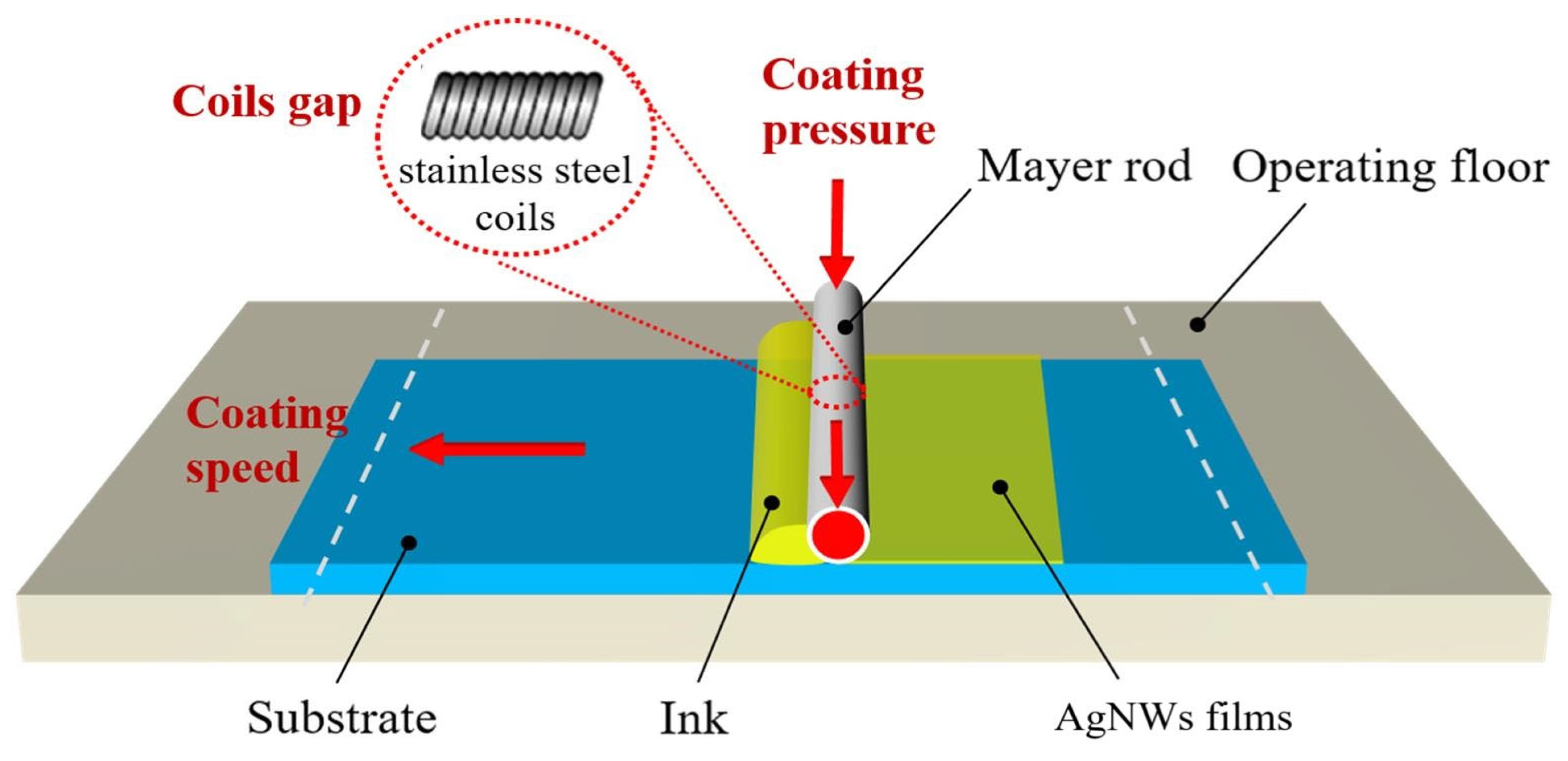
Figure 2.
Flowchart for the Preparation of AgNW-TCFs by Spray Deposition Method. (a) AgNWs solution, (b) canister, (c) nitrogen gas pressurization, (d) spray nozzle, (e) AgNWs droplets, (f) glass substrate in a vertical position, (g) hot plate (T = 100 ℃), and (h) the spray nozzle is moved up and down(arm speed = 100 mm/s) several times [26].
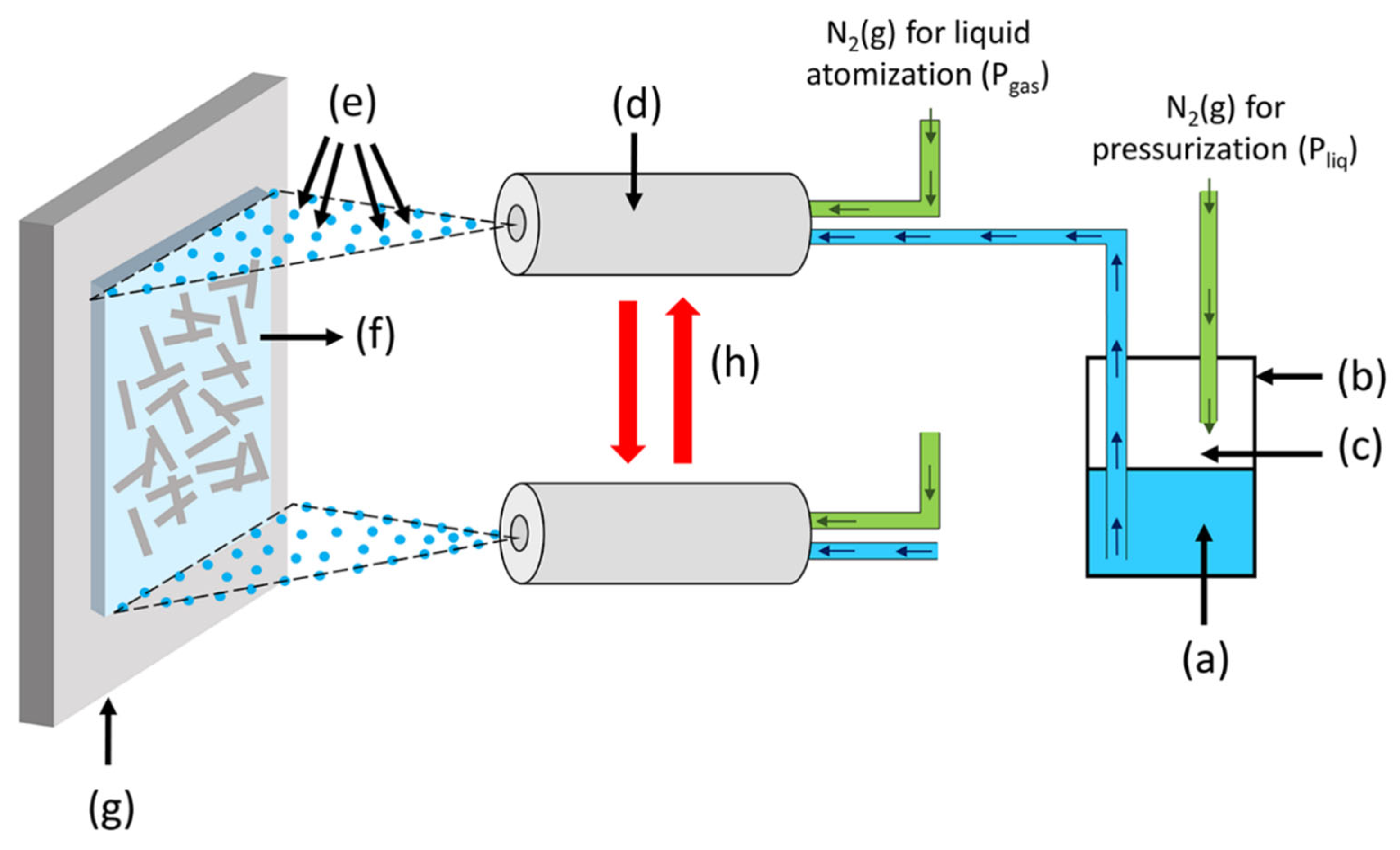
Figure 3.
Schematic diagram of the inkjet printing process [36].
Figure 3.
Schematic diagram of the inkjet printing process [36].
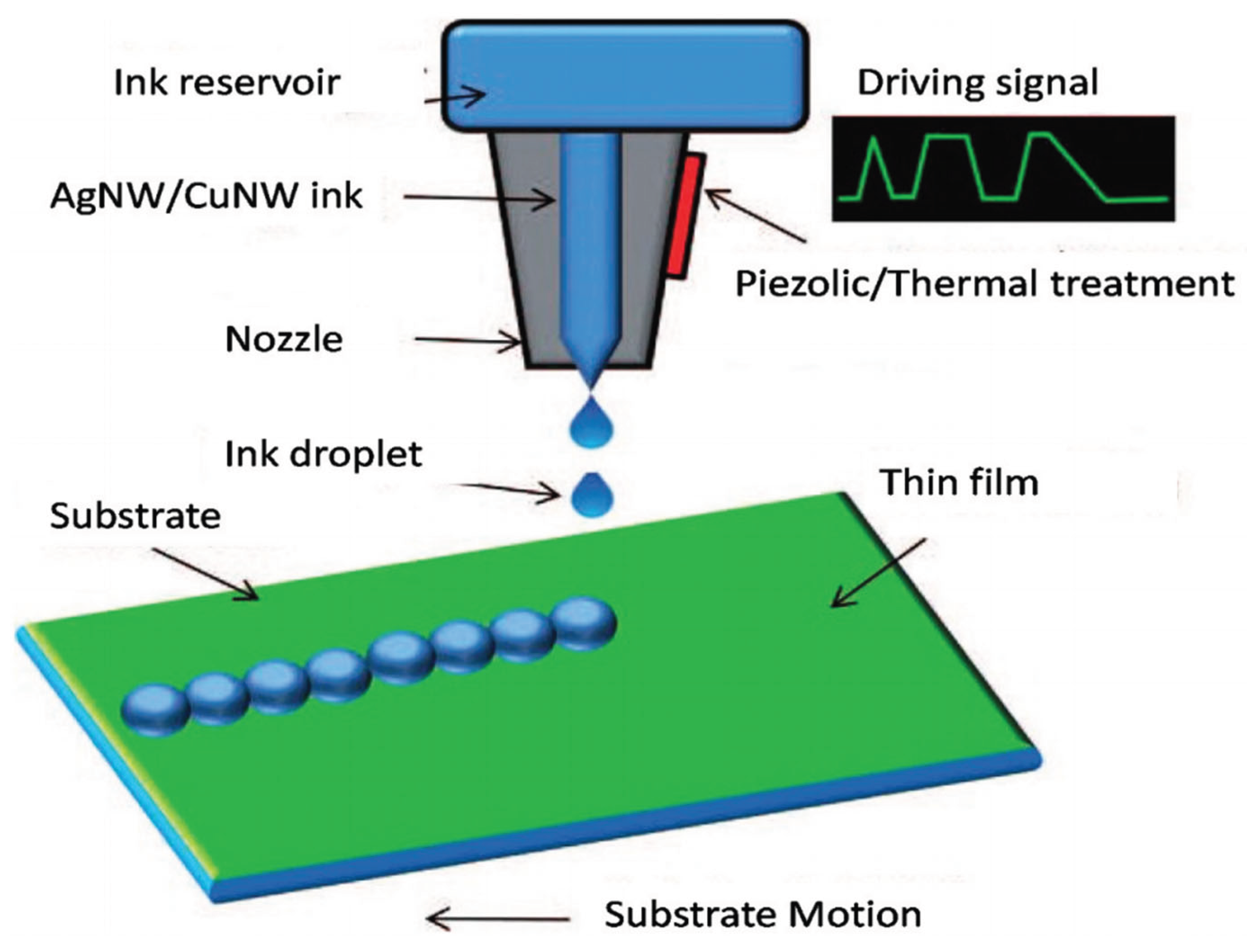
Figure 4.
The main features related to the coating of metallic nanowires depend on the coating process. MOx homogeneity, surface coverage, and conformality on the AgNWs depending on the method employed, namely (Ch.) chemical processes (a) Atomic layer deposition (ALD), (b) Chemical vapor deposition (CVD), and (Phys.) physical processes (c) Sputt, Evap, and Pulsed layer deposition (PLD) [41].
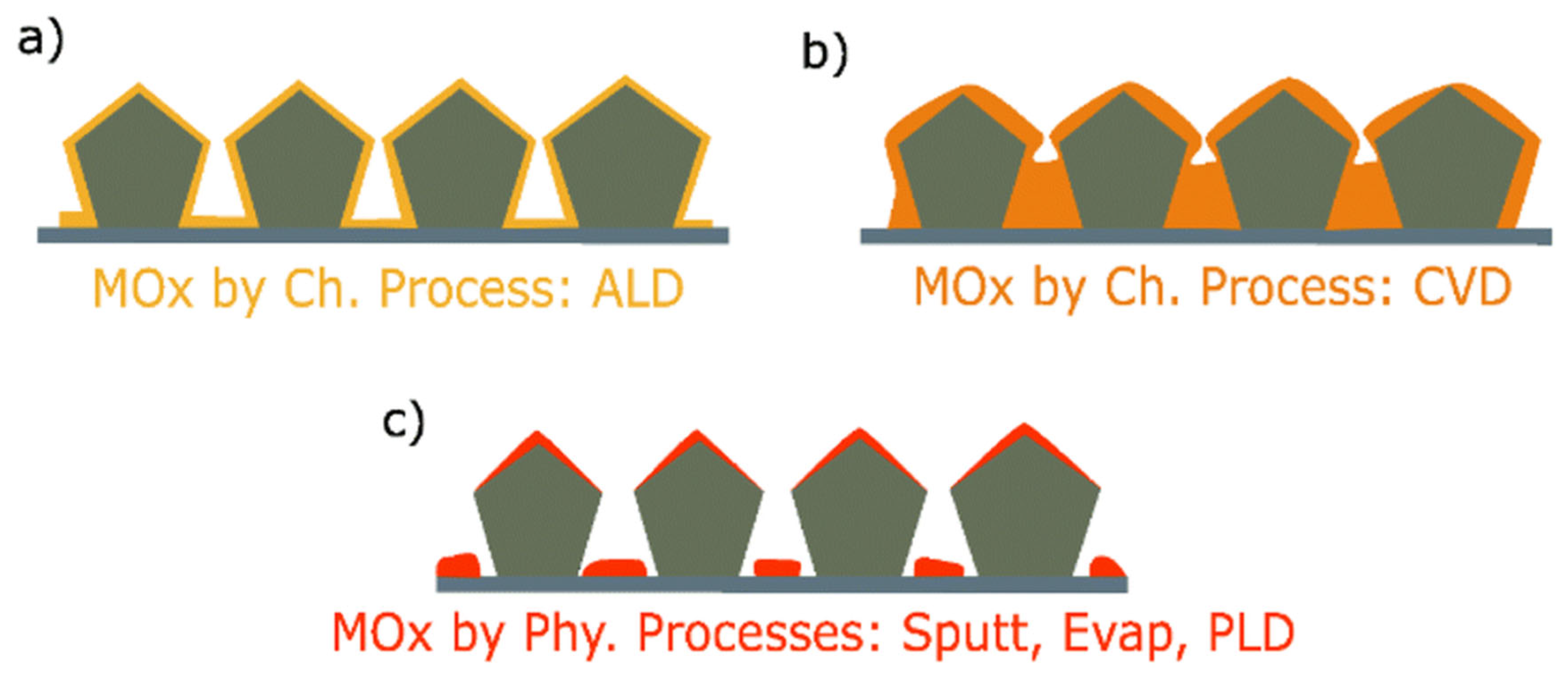
Figure 5.
General schemes of MOCVD and ALD processes [45].
Figure 5.
General schemes of MOCVD and ALD processes [45].
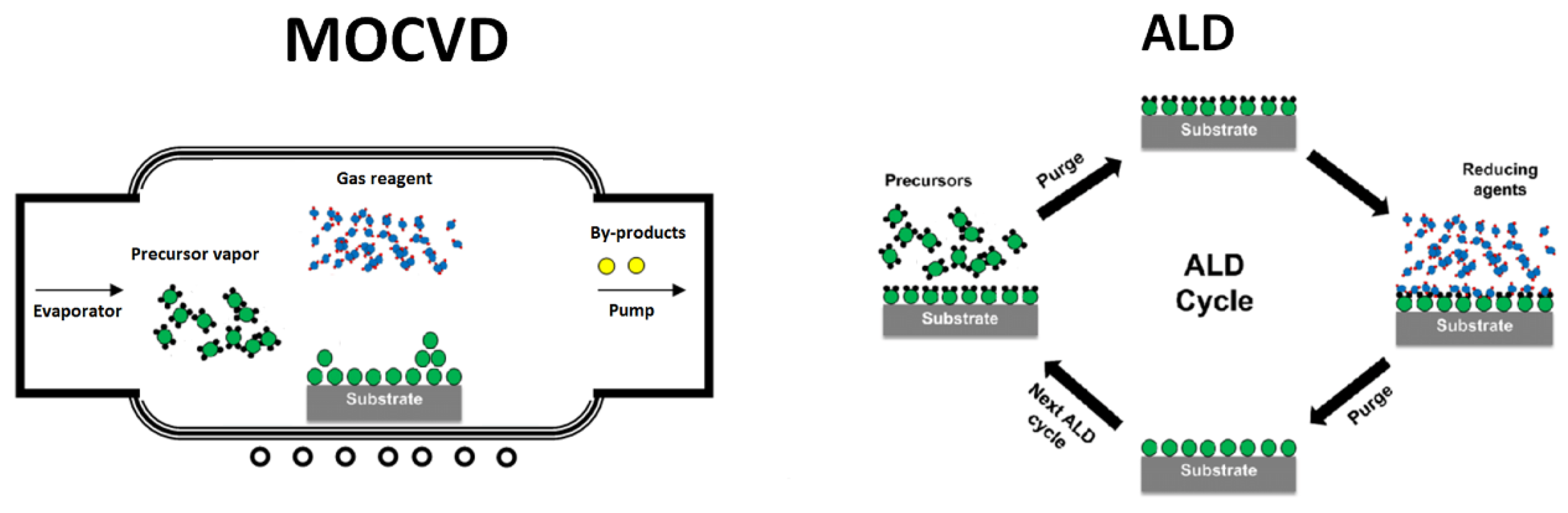
Figure 6.
(a) Schematic diagram of the structure of a large-area flexible transparent touch screen; (b) Demonstration of writing letters on the transparent touch screen recorded on the computer monitor; (c) Picture of tracking a butterfly under the transparent touch screen [49] (color online).
Figure 6.
(a) Schematic diagram of the structure of a large-area flexible transparent touch screen; (b) Demonstration of writing letters on the transparent touch screen recorded on the computer monitor; (c) Picture of tracking a butterfly under the transparent touch screen [49] (color online).
Figure 7.
The structure of FOSCs is based on AgNW films [60].
Figure 7.
The structure of FOSCs is based on AgNW films [60].
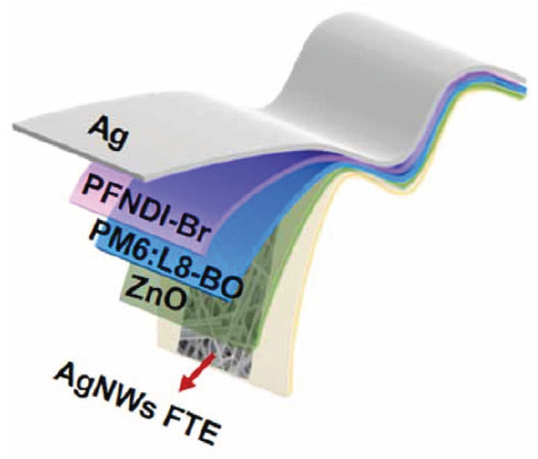

Table 1.
Performance parameters for different AgNW film deposition methods.
| Method of Film Deposition | Tav / % | Rs / Ω·sq-1 | FOM | Reference |
|---|---|---|---|---|
| Meyer Rod Coating | 92.2 | 12.9 | 352.33 | [11] |
| Meyer Rod Coating | 91 | 10 | 390.08 | [24] |
| Spraying | 91.7 | 9 | 709 | [26] |
| Spraying | 86.6 | 18.3 | 138 | [28] |
| Spin Coating | 82.6 | 9.4 | 199.78 | [29] |
| Spin Coating | 87.5 | 14.4 | 189.44 | [31] |
| Silk-screen printing | 95.3 | 13.6 | 568.47 | [33] |
| Inkjet Printing | 83.1 | 34.0 | 57.12 | [37] |
| Inkjet Printing | 74 | 2.9 | 399.74 | [38] |
Table 2.
Advantages and Disadvantages of Different Film-forming Processes.
| Preparation Method | Film Uniformity | Equipment Cost | Production Efficiency | Applicable Scenarios |
|---|---|---|---|---|
| Meyer Rod Coating | good | low | slow | small scale in the laboratory |
| Spin Coating | excellent (small area) |
Moderate (except high-precision) |
fast (small-area) | electronic, optical devices |
| Spraying | moderate (dependent on spray control) | moderate | fast | architectural glass, solar cells |
| Silk-screen printing | moderate (except for edges and corners) | low (except high-precision) |
fast | electronic circuits, sensors |
| Inkjet Printing | excellent (sprinkler head) |
high (spray head and ink) |
low (large-area) fast (small-area) |
microelectronics, Flexible Electronics, Biosensors |
Table 3.
Comparison Table of Characteristics and Typical Applications of AgNWs Prepared by Different Methods.
Table 3.
Comparison Table of Characteristics and Typical Applications of AgNWs Prepared by Different Methods.
| Preparation Method | Film Uniformity | Equipment Cost | Production Efficiency | Applicable Scenarios |
|---|---|---|---|---|
| Sputtering Deposition | excellent (dense, regular-structured) | high | medium | TCEs (e.g., displays, solar cells) |
| Pulsed layer deposition (PLD) | excellent (precise patterning) | very high | low (small-area) |
high-performance electronic devices (e.g., gas sensors, high-frequency electronic components) |
| Chemical vapor deposition (CVD) | excellent (large-area, high-quality) | very high | high (large-area) |
flexible electronic devices (e.g., flexible display screens, wearable devices) |
| Atomic layer deposition (ALD) | extremely high (atomic level) | very high | low (layer-by-layer deposition) | high-stability electrodes (e.g., lithium battery electrodes, UV photodetectors) |
| Solution methods | poor (porous structure) | low | relatively high | flexible wearable devices (e.g., flexible circuits, biosensors), low-cost optoelectronic devices |
Table 4.
Performance comparison of AgNWs applied to OLED.
| Material | Substrate | Area(cm2) | Turn-on voltage(V) | Maximum Current Efficiency(cd/A) | Maximum Luminance(cd/m2) | Reference |
|---|---|---|---|---|---|---|
| LPMN-processed AgNWs | PET | 2.5 × 2.5 | 3 | 78.0 | 5118 | [50] |
| Ti3C2Tx / AgNWs |
PEDOT: PSS |
4 × 4 | 7 | 3.7 | 10040 | [51] |
| HRLOC/ AgNWs |
PI | 20 × 20 | 18.37 | 20000 | [53] | |
| AgNWs | GLASS | 4 × 4 | 5.5 | 45.99 | 27310 | [55] |
| Graphene /AgNWs | PET | 9 | 15000 | [56] | ||
| AgNWs/ITO | PI | 1 × 1 | 7.7 | 5000 | [58] | |
| PVA/AgNWs | PEN | 10 | 35.3 | 18540 | [59] |
Disclaimer/Publisher’s Note: The statements, opinions and data contained in all publications are solely those of the individual author(s) and contributor(s) and not of MDPI and/or the editor(s). MDPI and/or the editor(s) disclaim responsibility for any injury to people or property resulting from any ideas, methods, instructions or products referred to in the content. |
© 2025 by the authors. Licensee MDPI, Basel, Switzerland. This article is an open access article distributed under the terms and conditions of the Creative Commons Attribution (CC BY) license (http://creativecommons.org/licenses/by/4.0/).
Copyright: This open access article is published under a Creative Commons CC BY 4.0 license, which permit the free download, distribution, and reuse, provided that the author and preprint are cited in any reuse.


