Submitted:
02 June 2025
Posted:
03 June 2025
You are already at the latest version
Abstract
The growing demand for electric vehicles, renewable energy, and portable electronics has increased the prevalence of power conversion systems, as exemplified by the architecture of electric automobiles. While silicon devices and circuits are widespread due to their cost-effectiveness, and structures such as the superjunction MOSFET have helped maintain its competitiveness in power applications, the technology remains fundamentally limited by its physical properties. Research and development in semiconductor technologies aim to reduce system size and improve power efficiency in these applications. The Gallium Nitride wide-bandgap semiconductor, with its critical electric field of 3.75 MV/cm, which is 12.5 times higher than that of silicon, has emerged as a strong candidate to meet these demands. This paper reviews key milestones of GaN technology; covering devices, compact modeling, packaging, circuit design, and converter implementation; highlighting its suitability for power electronics. For example, a monolithically integrated GaN Buck converter employing soft-switching achieves a peak efficiency of 95.4% when stepping down from 250V to 150V. In the case of a synchronous boost converter using discrete GaN transistors, delivered power can be increased by 37.5% while maintaining an efficiency of 99%. Additionally, GaN has enabled new converter topologies, achieving a power density of 123.3kW/L and an efficiency of 90.9%.
Keywords:
comparison
; converter
; dc-dc
; gallium
; GaN
; HEMT
; hybrid
; model
; monolithic
; nitride
; overview
; packaging
; power
; stage
; transistor
; wide-bandgap
1. Introduction
Power electronics (PE) has become one of the leading fields in engineering, driven by the ongoing digitization and electrification of modern infrastructure. Power conversion systems (PCS) are found in a wide range of applications, including server farms [1], electric vehicles [2], portable devices, household appliances, and renewable energy systems [3]. The growth of this field is fueled by the demand for higher energy efficiency, reduced system size, and the emergence of new technologies and topologies, such as [4] and [5].
To illustrate the widespread use of power conversion systems, Figure 1 presents the architecture of a fully electric vehicle. In this type of vehicle, two batteries are used: a high-voltage (HV) battery that powers the traction motors, and a low-voltage (LV) battery from which various lower-voltage power buses are derived. The system includes an onboard battery charger (OBC) that enables external charging of the HV battery by converting the grid’s AC voltage into the required HV DC voltage. The LV battery is charged from the HV battery via a DC-DC converter.
As shown in Figure 1, multiple vehicle subsystems are powered from the LV voltage rail. These include body electronics (BE), infotainment systems (INFO), and Advanced Driver Assistance Systems (ADAS). Each of these subsystems may use the LV supply bus to generate their specific required voltages. The electric traction motor is driven by an inverter that converts HV DC power into a three-phase AC voltage. This power architecture clearly demonstrates that numerous power conversions are necessary within such a complex system, with the majority being implemented using various topologies of switching converters (SC).
The lower right side of Figure 1 shows a block diagram of a switching converter (SC). Its main functional components are the control circuit, the switching block (SB), and the output LC filter composed of reactive elements [6]. Among these, the switching block has the most significant impact on the system’s overall efficiency. At its core is the power switch (PS), whose primary role is to transfer power from the source to the load. It operates in cycles, alternating between on and off states, driven by square-wave pulse signals generated by the control circuit.
An ideal PS turns on and off instantaneously, exhibits zero resistance when conducting, and blocks any voltage when turned off. In practice, however, PS devices are implemented using semiconductors that introduce several non-idealities, such as conduction resistance (), finite switching time, limited drain-to-source breakdown voltage (BV), and, in the case of diodes, a non-zero forward voltage drop [6]. These deviations from ideal behavior result in power losses within the PCS, reducing overall efficiency. Additionally, limitations such as low BV and slow switching speed can restrict the range of applications for a given semiconductor device.
While silicon (Si) is the most commonly used material for power devices, other semiconductors have also been explored. Gallium Arsenide (GaAs) is widely used in the radio frequency (RF) field [7], but it is not suitable for power applications due to its relatively low thermal conductivity of 0.5 compared to Si’s 1.5. At present, the primary commercial competitors for the PS role are Silicon Carbide (SiC) and Gallium Nitride (GaN), which are wide bandgap (WBG) semiconductors. These materials exhibit approximately and higher critical electric fields, respectively, enabling devices that can withstand higher BVs in the same or even smaller areas than Si based devices. Furthermore, the reduced area leads to lower parasitic capacitances, which in turn enable higher switching frequencies. At the system level, this allows for the use of smaller inductors and capacitors [8].
This work extends [9] and has the purpose to highlight the widespread use of PCSs and how their performance and implementation are influenced by the semiconductor technologies and device structures employed. Although several semiconducting materials are presented and compared; including Si, GaAs, SiC, and ultra-wide bandgap (UWBG) materials such as Aluminum Nitride (AlN) and -Gallium Oxide (-); the primary focus is on GaN technology. This material is explored in detail by synthesizing the performance data of various reported power transistors, emphasizing key advantages such as higher BVs in smaller device areas, switching frequencies exceeding 500 kHz, and improved current conduction enabled by higher electron mobility compared to Si.
Based on our evaluation of multiple GaN and Si power stage integrated circuits (ICs), the monolithic integration of PSs and drivers opens the path to high-efficiency, low-footprint PCSs. The use of GaN transistors over their Si counterparts can increase the delivered power by 37.5% while raising the efficiency from 97% to 99% in the case of a synchronous boost converter [10]. Furthermore, this technology can enable new converter topologies, such as a Hybrid point-of-load (POL) converter that achieves a power density of 123.3 kW/L with an efficiency of 90.9% [11].
The remainder of this paper is organized as follows. Section 2 presents several semiconductor technologies in the context of power applications, emphasizing the physical characteristics that make them suitable for this field. Section 3 focuses on GaN technology, detailing the types of devices fabricated in this process, the simulation model developed for the lateral device, and packaging solutions for emerging technologies. In Section 4, GaN monolithic circuit design is explored, addressing both digital and analog design challenges and summarizing the performance of various circuits. Section 5 highlights the efficiency improvements achieved through GaN devices and introduces converter topologies enabled by this technology. Finally, Section 6 concludes the paper.
2. Semiconductor Technologies for Power Conversion Applications
The application’s power rating and switching frequency dictate the choice of semiconductor device [12], as illustrated in Figure 2. For high power applications, Si thyristors are commonly used. In the medium to high power range, insulated-gate bipolar transistors (IGBTs) were traditionally the preferred choice. However, with the advent of SiC MOSFETs, the two technologies are now in competition. SiC MOSFETs offer several advantages, including an intrinsic body diode, whereas IGBTs require an external freewheeling diode on the printed circuit board (PCB) or integrated at package level. Additionally, SiC devices support higher switching frequencies than IGBTs [13].
For low to medium PCSs, Si MOSFETs compete with both SiC MOSFETs and GaN High Electron Mobility Transistors (HEMTs). These wide-bandgap devices offer superior performance in terms of voltage-blocking capabilities and switching speed, typically in smaller packages. SiC MOSFETs are favored for their higher BV and thermal conductivity, while GaN HEMTs are preferred for their fast switching capabilities [14].
The feasibility of using emerging WBG semiconductors as PSs stems from their superior physical properties. These materials offer higher critical electric fields, wider bandgaps, greater thermal conductivity, and improved electron mobility. A summary of the physical characteristics of various semiconductor materials is presented in Table 1 [7,15,16,17,18] with key parameters including band gap (), dielectric constant (), carrier mobility (), critical electric field (), electron saturation velocity (), and thermal conductivity (k).
GaAs offers a higher of 8.500 compared to Si’s 1.350, making it a preferred material for high-frequency applications such as optical switches and RF devices [7]. However, its low k of 0.5 limits its suitability for power applications. SiC, by contrast, is well-suited for high-power and high-voltage applications due to its ≈ higher thermal conductivity compared to GaAs and about higher than Si. It also serves as a suitable substrate for GaN devices [7]. GaN surpasses all the aforementioned materials in terms of and , while also exhibiting higher electron mobility than both Si and SiC. As a result, GaN based devices are widely adopted alongside SiC devices in commercial PCS due to their technological maturity and performance [19].
For future power devices, UWBG materials such as AlN, , and diamond are currently under research [15,16,17,18,20]. As shown in Table 1, offers promising characteristics compared to GaN, including an ≈ 2.1× higher and ≈1.4× higher , which could enable devices with even higher BVs in the future. AlN stands out with the highest of 15.9 among the listed materials, along with a high k of 3.21 , surpassed only by SiC and diamond. Among all presented semiconductors, diamond exhibits the best properties, with a ≈3.5× higher , ≈ 2.7× higher , and about ≈18.7× higher k compared to GaN. The remainder of this article will focus on developments based on GaN semiconductor technology.
3. GaN Technology
This chapter provides insight into the development of the standard GaN transistor structure and compares various lateral and vertical device implementations. It also covers specific aspects such as the industry-standard simulation model for this transistor and the packaging methods commonly used for these power devices.
3.1. GaN Devices
The first GaN transistors utilized a lateral Metal-Insulator-Semiconductor High Electron Mobility Transistor (MIS-HEMT) structure, as shown in Figure 3 a). In this implementation, a dielectric layer is inserted between the gate and the two-dimensional electron gas (2DEG) formed at the GaN - AlGaN heterojunction, resulting in a depletion-mode (d-mode) device. In such devices, the channel conducts by default, and electron flow can only be interrupted by applying a negative gate voltage, which repels charge carriers from the channel. Although these transistors offered performance advantages over their Si counterparts, their normally-on behavior was considered unsuitable for PE applications due to safety and control concerns. An early commercial solution to this limitation was the GaN-Si cascode structure, which combined a low-voltage Si MOSFET with a high-voltage GaN d-mode HEMT to create a normally-off, enhancement-mode (e-mode) configuration [10]. This approach also allowed for the integration of features such as gate driving and protection circuitry within the Si circuit [21].
To eliminate the need for additional components, various device-level modifications have been explored to create e-mode HEMTs. The most widely adopted solution is shown in Figure 3 b), where a p-doped GaN layer is introduced beneath the gate. This forms a reverse-biased Schottky junction, which creates a depletion region that suppresses the 2DEG channel under zero gate bias, thereby achieving normally-off behavior. To reach BVs in the range of 200V to 650V, a HV variant of the device is employed, as depicted in Figure 3 c). In this version, the drain region is extended, and field plates are added to redistribute the electric field away from the gate. Another approach to developing devices that leverage the advantages of GaN semiconducting material while exhibiting higher BVs, currents, and reliability than HEMTs is the use of vertical structures such as [22] and [23].
A milestone in GaN device development is the realization of the dual-gate bidirectional switch (BDS) [24]. This device operates in four modes: it blocks current when both gates are unbiased, functions as a switch when both gates are biased, and acts as a rectifier when only one gate is biased (true for either gate). BDSs are especially useful in SCs such as matrix converters, an AC-AC converter topology that eliminates the need for a DC-link capacitor. Traditionally, the switches in these topologies are implemented using two anti-series connected devices, such as MOSFETs or IGBTs. The GaN BDS offers advantages such as reduced cost, area, and , by utilizing a shared drift region. This innovation has already reached commercial availability [25].
An initial obstacle that hindered the widespread adoption of GaN devices was the difficulty of growing large GaN crystals suitable for wafer production [7]. The high cost associated with native GaN substrates led to the use of alternative materials such as Si, sapphire, and SiC. Among these, Si is the most cost-effective option, SiC offers improved thermal conductivity at a higher cost, and sapphire is typically used in RF and optoelectronic applications of GaN devices. Recently, a technological breakthrough enabled the production of 300mm wafers, a development that is expected to reduce GaN device prices in the long term [26].
Table 2 synthesizes multiple reported lateral and vertical devices. This GaN fin FET [23] offers more current conduction per area and lower on-resistance compared to the Current Aperture Vertical Electron Transistor (CAVET) reported in [22], while also reducing production cost by eliminating the need for epitaxial regrowth. The transistor reported in [27] exhibits the highest BV voltage among the lateral devices but also an undesirably low threshold voltage of 0.64V and higher than the other works presented. Both [28] and [29] HEMTs have very low values of and , respectively. The device in [28] has the advantage of a high BV of 1000 V but suffers from low current conduction. In contrast, the device presented in [29] has a BV of 420 V and boasts the highest current conduction among the HEMTs, reaching 0.86 . Although [22] has demonstrated the possibility of co-integrating HEMTs and CAVETs, the lateral device structure is still preferred for GaN monolithic circuit design.
3.2. GaN HEMT Model
Due to the structure of GaN transistors and the material-specific properties of GaN technology, standard SPICE models are inadequate for accurately capturing device behavior. To address this limitation, a physics-based compact model, known as the MIT Virtual Source GaN-HEMT (MVSG) model, has been adopted as an industry standard [30]. The equivalent circuit of the model is shown in Figure 4. The schematic illustrates five distinct regions of the device: the intrinsic transistor region under the gate, two field plate regions on the drain side that enhance the BV, and two access regions at the ends of the channel, modeled as implicit gate (gate voltage is on the schematic) transistors. The superimposed components in blue represent the modeled elements that define the device behavior. These components, implemented in Verilog-A, include: resistors modeling contact resistance; and modeling the gate-source and gate-drain capacitances; and , , , and modeling the capacitances between each field plate and the source or drain.
In [31], the authors emphasize the importance of accurately modeling device-level effects by developing an MVSG model that uses a charge-based approach to compute terminal currents. This model accounts for phenomena such as access-region depletion, dynamic thermal behavior, and charge-trapping effects. Its accuracy was validated through simulations of a HV Buck SC and an RF power amplifier. In the Buck converter case, the model accurately predicted the slew rate of the half-bridge switching node, demonstrating its effectiveness in capturing transient behavior. Further enhancements to the MVSG model have been proposed to include the behavior of the Schottky p-GaN gate. The validity and accuracy of this extension were confirmed through comparisons with experimental data and TCAD simulations [32].
3.3. GaN Packaging
The power losses in a PCS are converted into heat, which must be effectively dissipated to ensure reliable operation. As the temperature rises, the of power transistors increases, leading to even greater power losses. Additionally, excessive temperatures can cause irreversible damage to the device, making thermal management a critical aspect of PCS design. While WBG devices deliver superior performance in smaller die areas, this miniaturization inherently limits heat dissipation. These thermal challenges are further intensified by the demand for higher system power densities and reduced PCB footprint, necessitating cooling solutions that do not compromise miniaturization.
To meet these requirements, chip-scale (CS) packages have been adopted for GaN devices [33]. This packaging style improves the package-to-die size ratio, reducing overall packaging costs; which helps compensate for the higher material costs of GaN; and enhances thermal performance by eliminating additional thermal impedances introduced by traditional package methods.
In [34], the thermal performance of commercial chip-scale GaN power transistors was compared to that of Si power MOSFETs housed in various packages. To ensure a fair comparison between the two technologies, Buck converters were developed using each device. When comparing a GaN HEMT to a MOSFET in a CanPAK package, both operating without additional cooling and under a 30 A load, the GaN-based system demonstrated a 35% reduction in power losses at a switching frequency of 300 kHz, and a 40% reduction at 400 kHz. When equipped with a heatsink, the SC using GaN achieves an output current of 30 A while operating at 100°C, whereas its Si counterpart is limited to 20 A under the same thermal conditions. As a result, the GaN-based system delivers 50% higher output power at the same temperature.
Another advantage of CS packaging is the reduction of parasitic resistance and inductance. Thanks to the lateral structure of GaN HEMTs, there is no need for leadframes or bond wires to bring the drain, source, and gate terminals to the same plane. In contrast, Si power transistors typically use vertical structures, which place the drain and source on opposite sides of the die, requiring such interconnections. The reduced parasitic resistance helps further decrease , while the lower parasitic inductance enables higher switching frequencies with minimized voltage ringing. Reduced ringing, particularly on the gate signal, is crucial, as excessive oscillation can damage the gate terminal [35].
Ongoing research focuses on advancing packaging methods for emerging semiconductor technologies. In [36], the authors propose replacing traditional bond wires with copper clips and sintered copper paste to improve thermal and electrical performance. Meanwhile, [37] explores embedding the GaN die directly into the PCB and positioning the decoupling capacitor as close as possible to the die, significantly reducing parasitic inductance. These findings highlight that advanced packaging techniques are essential for emerging power semiconductor technologies to minimize parasitic elements and enhance thermal conductivity. Currently, GaN packaging improves performance through reduced thermal impedance enabled by the CS package and the use of redistribution layers with solder bumps or copper pillars, which reduce parasitic resistance and inductance while also providing an additional heat dissipation path.
4. GaN Monolithic Integrated Circuits
The high switching frequencies targeted by GaN devices pose a challenge due to the parasitic inductances inherent in the packaging, bond wires and PCB traces. Such phenomena can induce voltage ringing on the gate of GaN power transistors, potentially leading to destructive overshoot. To address this issue, the first approach was to package GaN HEMTs with Si gate drivers to minimize parasitics. To further reduce these inductances, monolithic integration of the control circuits and power transistor has emerged as a solution [38]. This chapter presents the adopted digital and analog design techniques used in this technology and reports and compares the performances of multiple GaN monolithic circuits.
4.1. Digital Design
The initial step in developing GaN ICs involves designing suitable digital circuits. Since commercial technologies lack a p-type GaN device, primarily due to the added fabrication complexity and the times lower transconductance [38], alternative logic families have been developed to overcome this limitation. These logic families primarily differ in their implementation of the pull-up (PU) network. The main types of logic families used in GaN ICs are presented in Figure 5 and respecting the notation from the figure they are described as follows: a) Resistor-Transistor Logic (RTL): In this family, the load is a resistor [39], b) Direct-Coupled FET Logic (DCFL): Here, the PU is a d-mode GaN device [40], c) Pseudo-Complementary FET Logic (PCFL): In this family, the load is an e-mode device controlled by a signal complementary to the input, resembling a push-pull stage [41], d1) Bootstrapped (BS) Logic: This logic family uses an enhancement-mode device as the PU, with its gate bootstrapped through a diode and a capacitor [42]. Due to its complementary control, the PCFL family has the lowest power consumption, while the BS family exhibits better noise margins with smaller devices when compared to DCFL [42]. Additionally, the enhancements to the BS logic family proposed in [43] are illustrated in Figure 5 d2), and consist of the addition of a PD device and a resistor (highlighted in blue), which effectively reduce static current. However, this modification results in a slower rise time.
Even though the complementary GaN device demonstrates inferior performance compared to its n-type counterpart, novel approaches for its utilization have been proposed, such as in [44]. In this work, the complementary device is employed to block leakage current paths and reduce static power consumption. Moreover, the use of this hybrid topology leads to improvements in both fan-out and propagation delay.
4.2. Analog Design
Power stages and switching regulators often incorporate protection circuits; such as overtemperature, overcurrent, and overvoltage protection; which are typically implemented using analog blocks. Furthermore, as demonstrated in [45,46,47], control loops in SCs are also realized using analog techniques.
One challenge in GaN analog design stems from the absence of p-type devices. The lack of complementary transistors imposes several constraints: it necessitates the use of resistors as loads, limits current mirrors to sinking-only configurations, and restricts the input common-mode range of differential pairs. Given the p-type current mirrors unavailability, large area resistors are used as loads when designing GaN-based amplifiers. As shown in [48], with only 20dB per amplification stage, multiple stages of differential amplification are required to achieve a gain of 60dB. A similar cascading approach is used in the comparator of the Buck converter presented in [47], where two amplifier stages are employed to attain a gain of 31dB.
The common-mode limitation of e-mode n-type-only GaN technologies comes from the high positive threshold voltage of the devices. As a result, input signals below this threshold require level shifting. Two solutions have been proposed: in [47], diode-connected HEMTs are used in the comparator to shift the input voltage levels, whereas in [45], a switched-capacitor technique is employed for level shifting.
Crystal defects in GaN degrade device matching, imposing an additional constraint on analog design. In [38], the matching performance of various fundamental analog building blocks was evaluated. A resistive divider demonstrated a mismatch standard deviation of between its resistors and an absolute resistance variation of across the wafer. These resistors are implemented using 2DEG channels formed from HEMTs without gates. However, due to back-gating effects in the upper device, its resistance is consistently higher than that of the lower device. Threshold voltage measurements reported in [10] show that standard HEMT structures exhibit a variation of , whereas structures with a modified gate reduce this variation to . These mismatches significantly impact analog circuits, especially differential pairs, resulting in input-referred offsets as high as .
A solution to mismatch in current mirrors is the use of source degeneration, as resistors are expected to exhibit less variation compared to HEMTs due to the absence of the layers required to form the p-GaN gate [38]. This approach has been implemented in the level shifter of the power stage described in [49], although no data is reported regarding the accuracy of current matching. To address mismatch in differential stages, auto-zeroing and chopping techniques can be applied, as demonstrated in the comparator from [50], which successfully reduces the input offset from 112mV to 1.2mV.
4.3. Power Circuits
To overcome the limitations imposed by parasitic inductance on the switching frequency of GaN transistors, monolithic integration of the driver and the PSs on a single die has been adopted, resulting in a power stage circuit. Various research implementations of such circuits are enabled by one or more of the previously discussed logic families. For example, the GaN half-bridge circuit in [49] employs a combination of RTL and PCFL logic, while the design in [39] exclusively uses RTL gates. Additionally, the commercial GaN IC presented in [51] is based on the BS logic gates family.
The characteristics of multiple power stages are summarized in Table 3. The IC detailed in [52] exhibits the slowest switching frequency and the highest , serving as a reference Si power stage. The multi-die approach from [53], which combines Si control with GaN PSs, stands out among the listed circuits by achieving the lowest at 4.4 m, the highest drain current of 35 A, and the second-highest switching frequency of 10 MHz.
The power stage presented in [54] integrates switches with an of 30 m, the second-lowest value in the table, and supports a high switching frequency of 25 MHz. The design utilizes the modified BS logic gate family shown in Figure 5 d2) to enhance PU speed and reduce static power consumption. While it results in higher power consumption at lower frequencies, it achieves lower power consumption in the 25–30 MHz range compared to a commercial Si driver. It also features a level shifter with high common-mode transient immunity, as well as an adaptive PD switch that prevents signal loss during freewheeling. The circuit presented in [55] employs a segmented, binary-weighted driver to control the voltage slopes of the gate and drain terminals. This approach effectively reduces gate voltage oscillations, thereby preventing the potential damage of this terminal. The power stage presented in [56] exhibits the highest dynamic power loss, due to its RTL driver implementation. Although this work does not propose a complex design, it compares the circuit’s performance with simulation results based on the MVSG model for the HV device, showing a maximum error of 21.2% in the switching time parameter. In [49], a novel protection method for the high-side latch in the level shifter is proposed. The drivers are implemented using RTL gates that control two push-pull stages in a PCFL configuration, reducing power consumption in the stages with higher output current capability. Two different supply voltages are used to configure the resistance of the PU devices and mitigate voltage overshoots at the gates of the PSs. The commercial circuit in [51] employs the BS logic family and is the only GaN power stage that integrates a bootstrap switch for the high-side driver; all other implementations use an external diode. It supports a maximum operating current of 40 mA at 3 MHz, while the BS power stage from [54] achieves a current consumption of 20 mA at 5 MHz. The circuit also includes an undervoltage lockout block that enables operation only when the supply voltage exceeds a specified threshold.
Another promising type of power circuit for GaN monolithic integration is the switching regulator, which is a system that incorporates a power stage and a control loop. Multiple Buck SCs have been reported [45,46,47].
The circuit presented in [45] is realized in an e-mode 650V GaN technology, occupies an area of 2.1 and achieves an efficiency of 95.6% for an input of 85V. The control loop operates in boundary conduction mode. It integrates a zero voltage detector (ZVD) and reads the output current through a shunt resistor. When the switching node reaches zero volts, the driver control signal is set high, and when the current reaches a peak value determined by an external voltage reference, the signal is set low. This way, the average current is set by the reference voltage.
A GaN Buck converter for server POL applications is proposed in [46]. It is designed in a 200V GaN-on-SOI technology, and for a load of 3A and a switching frequency of 250kHz, it achieves an efficiency of 84.3% when stepping down from 48V to 1V. The integrated feedback loop employs voltage mode control.
In this work [47], a SC fabricated in a 650V GaN technology is presented. The circuit converts from 400V to 48V, occupies an area of 16.25, and achieves an efficiency of 93.1%. A peak efficiency of 95.4% is reached when stepping down from 250V to 150V. The converter employs a constant-on-time (COT) control method and integrates a ZVD, which enables soft switching of the low-side transistor, resulting in up to a 5.5% efficiency improvement. The minimum on and off times of the control loop are trimmed using 5-bit and 3-bit resolution, respectively, through adjustment of a binary-weighted capacitor bank. The power stage can operate at frequencies up to 3.5MHz, but the COT controller is capable of generating control signals only up to 1.7MHz.
5. GaN Power Converters Evaluation
In [10], the authors evaluate the performance improvements offered by GaN transistors over their Si counterparts in Boost converters, considering both synchronous and non-synchronous topologies. The non-synchronous converter operates at a frequency of 500 kHz and, in continuous conduction mode (CCM), achieves a peak efficiency of 98.2% with the Si device, while the GaN version achieves 98.5% with a flatter efficiency curve at higher loads. The synchronous Boost converter operates at 100 kHz; the Si version could deliver only 2.4 kW of power due to overheating at higher loads, achieving a peak efficiency of 97%. In contrast, the GaN implementation could deliver 37.5% more power while exhibiting an efficiency of 99%.
The emergence of GaN technology, with its small footprint and high switching frequencies, has enabled a wide range of GaN power converter-based applications, including satellites, augmented reality systems, and robotics [10]. The use of GaN devices has also facilitated hybrid SC topologies, such as those in [58] and [11]. The inverter reported in [58] utilizes 10 inductors enabled by high switching frequencies, achieving an efficiency of 98.6% and a power density of 35.3 kW/L. This PCS was developed as a lightweight solution for aircraft electrification. Moreover, due to their higher BV and radiation tolerance, these devices are well-suited for space applications, enabling compact, high-efficiency PCS, as demonstrated in [11]. This POL converter achieves a peak efficiency of 90.9% and a power density of 123.3 kW/L. For the same area reduction and efficiency benefits, GaN ICs have been adopted in commercial portable chargers, such as those in [59,60].
The author’s forecast for the development of GaN technology is outlined in the following paragraphs. In the case of discrete devices, the advancement of 300 mm GaN wafers is expected to enable the fabrication of vertical devices capable of withstanding BVs exceeding 1200 V. These devices will compete with IGBTs and SiC-based components, positioning GaN technology within the mid- to high-power range of the power semiconductor spectrum.
For IC technologies, GaN-based solutions are anticipated to incorporate a broader variety of devices, including fuse elements, which would allow on-chip parameter calibration directly within the power stage, eliminating the need for external Si based circuitry. Device structures will be optimized for both cost and electrical performance, with particular attention to parameter variation and manufacturing yield. Furthermore, as reported by Intel in [61], hybrid integration of Si and GaN is feasible, suggesting that growing HEMT power devices directly on a Si driver could become a practical approach.
At present, monolithic GaN power stages have gained traction in portable applications such as chargers, drones, and robots. However, wider adoption is anticipated in data center servers and in hybrid or fully electric vehicles, particularly for DC-DC converters between the system’s HV and LV batteries. Upon the commercial release of devices with a BV of 1200 V, GaN is expected to be adopted in traction inverters and OBCs as well.
Due to the small form factor of GaN devices and the benefit of enabling smaller reactive components we can expect to see a rise in compact system-in-package (SiP) designs. Regarding packaging, CS packages are widely used across semiconductor technologies due to their low cost, small footprint, reduced parasitics, and goode thermal conduction. Thermal performance can be enhanced by adding thermal pads that facilitate the attachment of heat sinks. A potential implementation has been investigated in [62], where the backside of the die is removed to allow filling with a high thermal conductivity material, such as copper. This technique could be applied to both SiPs mounted on PCBs and chips employing CS packaging.
6. Conclusion
This paper presented the need for efficient, high power density PCS. It showed that, while Si is currently used across a wide range of power applications, its performance is fundamentally limited by its physical properties. As alternatives, several semiconductor technologies were discussed, including WBG and UWB materials, with a focus on GaN. By reviewing key advancements in GaN technology; spanning fabrication processes, device design, compact modeling, packaging, circuit implementation, and converter architectures; this work demonstrated its suitability for next-generation power electronics. Through its high switching frequency, small footprint, and low , GaN technology has been shown to meet the demands for high efficiency and power density in applications such as portable chargers, electric vehicles, and satellites. This was supported by reported performance examples, such as a monolithically integrated GaN Buck converter achieving 95.4% peak efficiency when stepping down from 250V to 150V, and a synchronous Boost converter using discrete GaN transistors, which delivered 37.5% more power while maintaining 99% efficiency. GaN devices have also enabled new converter topologies, including hybrid inverters and hybrid POL converters, and have improved the feasibility and cost-effectiveness of topologies like the matrix converter. Thus, GaN power devices, through their superior physical properties, have surpassed Si in low to mid power applications. With continued technological advancements, GaN could compete with SiC in the mid to high power range and approach its theoretical limits; eventually to be surpassed by future UWBG materials.
Funding
This work was funded from the project "National Platform for Semiconductor Technologies", contract no. G 2024-85828/390008/27.11.2024, SMIS code 304244, co-funded by the European Regional Development Fund under the Program for Intelligent Growth, Digitization, and Financial Instruments.
Abbreviations
The following abbreviations are used in this manuscript:
| ADAS | Advanced Driver Assistance Systems |
| AlN | Aluminum Nitride |
| BDS | Bidirectional Switch |
| BE | Body Electronics |
| BS | Bootstrapped |
| BV | Breakdown Voltage |
| CAVET | Current Aperture Vertical Electron Transistor |
| CCM | Continuous Conduction Mode |
| COT | Constant-On-Time |
| CS | Chip-scale |
| DCFL | Direct-Coupled FET Logic |
| GaAs | Gallium Arsenide |
| GaN | Gallium Nitride |
| HEMTs | High Electron Mobility Transistors |
| HV | High Voltage |
| IC | Integrated Circuit |
| IGBT | Insulated Gate Bipolar Transistor |
| INFO | Infotainement |
| LV | Low Voltage |
| MIS-HEMT | Metal-Insulator-Semiconductor HEMT |
| MVSG | MIT Virtual Source GaN-HEMT |
| OBC | Onboard Battery Charger |
| PCB | Printed Circuit Board |
| PCFL | Pseudo-Complementary FET Logic |
| PCS | Power Conversion System |
| PD | Pull-Down |
| PE | Power electronics |
| POL | Point-Of-Load |
| PS | Power Switch |
| PU | Pull-Up |
| RTL | Resistor-Transistor Logic |
| RF | Radio Frequency |
| SC | Switching Converter |
| SB | Switching Block |
| Si | Silicone |
| SiC | Silicone Carbide |
| SiP | System in Package |
| UWBG | Ultra Wide Bandgap |
| WBG | Wide Bandgap |
| ZVD | Zero Voltage Detector |
References
- Krein, P.T. Data center challenges and their power electronics. CPSS Transactions on Power Electronics and Applications 2017, 2, 39–46.
- Chan, C.; Chau, K. An overview of power electronics in electric vehicles. IEEE Transactions on Industrial Electronics 1997, 44, 3–13. [CrossRef]
- Panigrahi, S.; Thakur, A. Current trends in power electronics for wind and solar energy conversion systems. In Proceedings of the ICPEDC, 2017, pp. 242–247.
- Devices, A. LTC7821, 2018. Datasheet. Accessed: May 17, 2025. [Online].
- van Wyk, J.D.; Lee, F.C. On a Future for Power Electronics. IEEE Journal of Emerging and Selected Topics in Power Electronics 2013, 1, 59–72.
- Erickson, R.W.; Maksimovic, D., Fundamentals of Power Electronics, 3rd ed.; Springer Cham, 2020.
- Gaudenzio Meneghesso, M.M.; Zanoni, E., Gallium Nitride-enabled High Frequency and High efficiency Power Conversion, 1st ed.; Springer Cham, 2018.
- intersil. HIGH FREQUENCY POWER CONVERTERS. https://www.analog.com/media/en/technical-documentation/tech-articles/an9208.pdf, 1994. Application Note Accessed: Dec. 21, 2024. [Online].
- Medinceanu, P.C.; Enachescu, M. An Overview of GaN Technology for Power Conversion Applications. In Proceedings of the ISETC, 2024, pp. 1–4.
- Chen, K.J.; Häberlen, O.; Lidow, A.; Tsai, C.l.; Ueda, T.; Uemoto, Y.; Wu, Y. GaN-on-Si Power Technology: Devices and Applications. IEEE Transactions on Electron Devices 2017, 64, 779–795. [CrossRef]
- Ellis, et al., N.M. Gallium Nitride-based 48V-to-1V Point-of-Load (PoL) Converter for Aerospace Telecommunications and Computing Applications. In Proceedings of the IEEE APEC, 2024, pp. 1384–1388.
- Park, J.M. Novel Power Devices for Smart Power Applications, 2004. Dissertation.
- Slawinski, M.; Heer, D.; Villbusch, T.; Buschkuehle, M. System study of SiC MOSFET and Si IGBT power module performance using a bidirectional buck-boost converter as evaluation platform. In Proceedings of the EPE’16 ECCE Europe, 2016, pp. 1–8.
- Palmer, P.; Zhang, X.; Shelton, E.; Zhang, T.; Zhang, J. An experimental comparison of GaN, SiC and Si switching power devices. In Proceedings of the IECON, 2017, pp. 780–785.
- Wort, C.J.; Balmer, R.S. Diamond as an electronic material. Materials Today 2008, 11, 22–28.
- Masataka Higashiwaki, Kohei Sasaki, A.K.T.M.; Yamakoshi, S. Development of gallium oxide power devices. PSS Applications and materials science 2014, 211, 21–26.
- Jinqiao Xie, Seiji Mia1, R.D.R.C.A.R.J.T.; Sitar, Z. Ni/Au Schottky diodes on AlxGa1-xN (0.7<x<1) grown on AlN single crystal substrates. PSS Current topics in solid state physics 2011, 8, 2407–2409.
- Tsao, J.Y.; Hollis, M.A.; Kaplar, R.J. Ultrawide-Bandgap Semiconductors: Research Opportunities and Challenges. Advanced Electronic Materials 2018, 4. [CrossRef]
- Li, J. The Emerging Adoption and Future Trends of SiC and GaN in EVs. https://www.idtechex.com/en/research-article/the-emerging-adoption-and-future-trends-of-sic-and-gan-in-evs/31201, 2024. Accessed: May 17, 2025. [Online].
- Zorpette, G. The Next Powerhouse Transistor For controlling high voltages, aluminum nitride will be hard to beat, 2024. Accessed: Dec. 21, 2024. [Online].
- Instruments, T. LMG341xR050, 2018. Datasheet. Accessed: May 17, 2025. [Online].
- Döring, P.; Driad, R.; Reiner, R.; Waltereit, P.; Leone, S.; Mikulla, M.; Ambacher, O. Technology of GaN-Based Large Area CAVETs With Co-Integrated HEMTs. IEEE Transactions on Electron Devices 2021, 68, 5547–5552. [CrossRef]
- Zhang, Y.; Sun, M.; Piedra, D.; Hu, J.; Liu, Z.; Lin, Y.; Gao, X.; Shepard, K.; Palacios, T. 1200 V GaN vertical fin power field-effect transistors. In Proceedings of the IEEE IEDM, 2017, pp. 9.2.1–9.2.4. [CrossRef]
- Baratella, G.; Chatterjee, U.; Syshchyk, O.; Borga, M.; Fabris, E.; Cosnier, T.; Bakeroot, B.; Decoutere, S. Monolithic 650-V Dual-Gate p-GaN Bidirectional Switch. IEEE Transactions on Electron Devices 2024, 71, 6904–6909. [CrossRef]
- Infineon. Infineon announces CoolGaN™ bidirectional switch and CoolGaN Smart Sense for higher performance and more cost-effective power systems, 2024.
- Infineon. Infineon pioneers world’s first 300 mm power gallium nitride (GaN) technology – an industry game-changer. https://www.infineon.com/cms/en/about-infineon/press/press-releases/2024/INFXX202409-142.html, 2024. Accessed: May 16, 2025. [Online].
- Chu, R.; Corrion, A.; Chen, M.; Li, R.; Wong, D.; Zehnder, D.; Hughes, B.; Boutros, K. 1.2 kV Normally Off GaN-on-Si FET With Low Dynamic on Resistance. IEEE Electron Device Letters 2011, 32, 632–634.
- Hilt, O.; Brunner, F.; Cho, E.; Knauer, A.; Bahat-Treidel, E.; Würfl, J. Normally-off high-voltage p-GaN gate GaN HFET with carbon-doped buffer. In Proceedings of the IEEE ISPSD, 2011, pp. 239–242. [CrossRef]
- Imada, T.; Kanamura, M.; Kikkawa, T. Enhancement-mode GaN MIS-HEMTs for power supplies. In Proceedings of the ECCE ASIA, 2010, pp. 1027–1033.
- Radhakrishna, U.; Antoniadis, D. MIT Virtual Source GaN HEMT-High Voltage (MVSG-HV) compact model. https://nanohub.org/publications/73/1, 2015. Accessed: May 17, 2025. [Online].
- Radhakrishna, U.; Choi, P.; Antoniadis, D.A. Facilitation of GaN-Based RF- and HV-Circuit Designs Using MVS-GaN HEMT Compact Model. IEEE Transactions on Electron Devices 2019, 66, 95–105. [CrossRef]
- Alaei, M.; Borga, M.; Fabris, E.; Decoutere, S.; Lauwaert, J.; Bakeroot, B. Extending Electrostatic Modeling for Schottky p-GaN Gate HEMTs: Uniform and Engineered p-GaN Doping. IEEE Transactions on Electron Devices 2024, 71, 5949–5955. [CrossRef]
- Lidow, A. Six Reasons to Rethink Power Semiconductor Packaging. https://epc-co.com/epc/about-epc/gan-talk-blog/post/13424/six-reasons-to-rethink-power-semiconductor-packaging, 2016. Accessed: May 17, 2025. [Online].
- Reusch, D.; Strydom, J.; Lidow, A. Thermal Evaluation of Chip-Scale Packaged Gallium Nitride Transistors. IEEE Journal of Emerging and Selected Topics in Power Electronics 2016, 4, 738–746.
- Kaufmann, M.; Seidel, A.; Wicht, B. Long, Short, Monolithic - The Gate Loop Challenge for GaN Drivers: Invited Paper. In Proceedings of the IEEE CICC), 2020, pp. 1–5.
- Ain, K.N.; Zhang, G.Q.; Rodrigues, A.; Hasan, M.N.; Holzmann, D.; Geens, K.; Chatterjee, U.; Roshanghias, A. An Introduction to Wire-Bondless Discrete GaN Power Packages With Top-Side Cu Sinterconnects®. In Proceedings of the IEEE ESTC, 2024, pp. 1–5.
- Moench, S.; Reiner, R.; Waltereit, P.; Benkhelifa, F.; Hückelheim, J.; Meder, D.; Zink, M.; Kaden, T.; Noll, S.; Mansfeld, S.; et al. PCB-Embedded GaN-on-Si Half-Bridge and Driver ICs With On-Package Gate and DC-Link Capacitors. IEEE Transactions on Power Electronics 2021, 36, 83–86.
- Kaufmann, M.; Wicht, B. Monolithic Integration in E-Mode GaN Technology, 1st ed.; Springer Cham, 2022.
- Li, X.; Amirifar, N.; Geens, K.; Zhao, M.; Guo, W.; Liang, H.; You, S.; Posthuma, N.; Jaeger, B.D.; Stoffels, S.; et al. GaN-on-SOI: Monolithically Integrated All-GaN ICs for Power Conversion. In Proceedings of the IEDM, 2019, pp. 4.4.1–4.4.4.
- Zhu, et al., M. Monolithic integration of GaN-based NMOS digital logic gate circuits with E-mode power GaN MOSHEMTs. In Proceedings of the IEEE ISPSD, 2018, pp. 236–239.
- Basler, M.; Moench, S.; Reiner, R.; Waltereit, P.; Quay, R.; Kallfass, I.; Ambacher, O. A Pseudo-Complementary GaN-Based Gate Driver with Reduced Static Losses. In Proceedings of the IEEE WiPDA, 2019, pp. 93–98.
- Medinceanu, P.C.; Enachescu, M. Analysis of the Bootstrapped GaN Logic Gate Family. In Proceedings of the IEEE CAS, 2024, pp. 229–232.
- Daniel M. Kinzer, Santosh Sharma, J.J.Z. GaN CIRCUIT DRIVERS FOR GaN CIRCUIT LOADS, US20160079854A1.
- Ma, S.; Jiang, Q.; Huang, S.; Wang, X.; Liu, X. A GaN-Based Hybrid Logic Circuitry With Low Power Consumption and Enhanced Fan-Out Capability. IEEE Transactions on Electron Devices 2025, 72, 618–624.
- Kaufmann, M.; Lueders, M.; Kaya, C.; Wicht, B. 18.2 A Monolithic E-Mode GaN 15W 400V Offline Self-Supplied Hysteretic Buck Converter with 95.6% Efficiency. In Proceedings of the IEEE ISSCC, 2020, pp. 288–290.
- Wu, S.; Ran, Z.; Tong, Z.; Liu, T.; Lu, Y. A Monolithic Integrated E-Mode GaN 48V-to-1V DC-DC Buck Converter with PWM Control. In Proceedings of the IEEE ICTA, 2023, pp. 130–131.
- Grobe, J.; Weihs, L.; Hanhart, M.; Wunderlich, R.; Heinen, S. Monolithic Integration of a 400V GaN Half-Bridge Converter With Output Voltage Regulation. IEEE Transactions on Circuits and Systems II: Express Briefs 2024, 71, 4591–4595. [CrossRef]
- Pennisi, S.; Pulvirenti, F.; Samperi, K. Frequency Compensation Scheme for a Full GaN OpAmp driving 1-nF load. In Proceedings of the IEEE ISCAS, 2022, pp. 2042–2046.
- Deneke, N.; Wicht, B. A 500-V, 6.25-MHz GaN-IC With Gate Driver and Level Shifter for Off-Line Power Supplies. IEEE Solid-State Circuits Letters 2024, 7, 207–210. [CrossRef]
- Grobe, J.; Zoche, J.; Wunderlich, R.; Heinen, S. An Auto-Zero Comparator for Monolithic GaN Power Integration. In Proceedings of the PRIME, 2024, pp. 1–4.
- EPC. EPC2152, 2021. Datasheet. Accessed: May 17, 2025. [Online].
- Systems, M.P. MP8040, 2011. Datasheet. Accessed: May 17, 2025. [Online].
- Instruments, T. LMG2100R044, 2023. Datasheet. Accessed: May 17, 2025. [Online].
- Lai, R.; Zhou, Z.; Wu, J.; Dai, Y.; Liu, X.; Zhang, B.; Shi, Y.; Li, S.; Qin, Z. A Monolithic GaN Power Stage With Common-Mode Transient Immunity and Negative Voltage Operation Design for High-Frequency Power Converters. IEEE Transactions on Power Electronics 2024, 39, 8129–8145. [CrossRef]
- Jiang, W.L.; Kadee Murray, S.; Zaman, M.S.; De Vleeschouwer, H.; Roig, J.; Moens, P.; Trescases, O. Monolithic Integration of a 5-MHz GaN Half-Bridge in a 200-V GaN-on-SOI Process: Programmable dv/dt Control and Floating High-Voltage Level-Shifter. In Proceedings of the IEEE APEC, 2021, pp. 728–734.
- Yamashita, Y.; Stoffels, S.; Posthuma, N.; Decoutere, S.; Kobayashi, K. Monolithically Integrated E-mode GaN-on-SOI Gate Driver with Power GaN-HEMT for MHz-Switching. In Proceedings of the IEEE WiPDA, 2018, pp. 231–236.
- Deneke, N.; Wicht, B. 31.10 A Fully integrated 500V, 6.25MHz GaN-IC for Totem-Pole PFC Off-Line Power Conversion. In Proceedings of the IEEE ISSCC, 2024, Vol. 67, pp. 514–516.
- Pallo, N.; Foulkes, T.; Modeer, T.; Coday, S.; Pilawa-Podgurski, R. Power-dense multilevel inverter module using interleaved GaN-based phases for electric aircraft propulsion. In Proceedings of the IEEE APEC, 2018, pp. 1656–1661.
- Navitas. Dell Adopts Navitas GaNFast Technology for Laptop Fast Charger. https://navitassemi.com/dell-adopts-navitas-ganfast-technology-for-laptop-fast-charger/, 2020. Accessed: May 17, 2025. [Online].
- Navitas. Navitas Goes Global in Xiaomi’s Mi 11 Fast Charger. https://navitassemi.com/navitas-goes-global-in-xiaomis-mi-11-fast-charger/, 2021. Accessed: May 17, 2025. [Online].
- Then, H.W.; Radosavljevic, M.; Bader, S.; Zubair, A.; Vora, H.; Nair, N.; Koirala, P.; Beumer, M.; Nordeen, P.; Vyatskikh, A.; et al. DrGaN: an Integrated CMOS Driver-GaN Power Switch Technology on 300mm GaN-on-Si with E-mode GaN MOSHEMT and 3D Monolithic Si PMOS. In Proceedings of the IEDM, 2023, pp. 1–4.
- Reiner, R.; Gerrer, T.; Weiss, B.; Waltereit, P.; Moench, S.; Meder, D.; Sinnwell, M.; Dammann, M.; Quay, R.; Ambacher, O. Si-Substrate Removal for AlGaN/GaN Devices on PCB Carriers. In Proceedings of the ISPSD, 2020, pp. 286–289.
Figure 1.
Power architecture, from system to semiconducting device
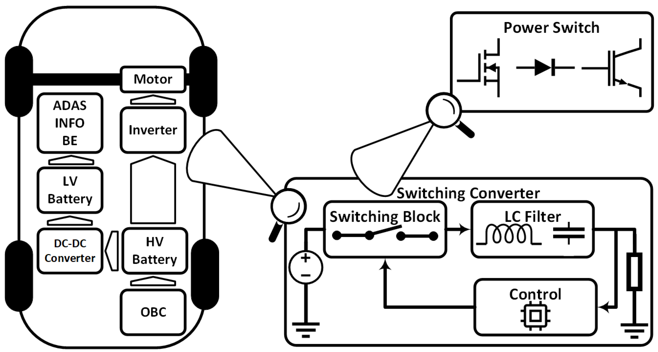
Figure 2.
Device distribution across different power levels
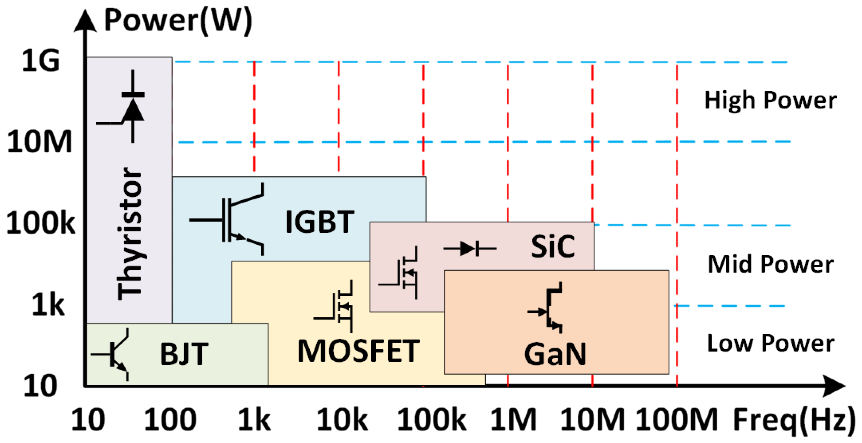
Figure 3.
GaN devices: a)MIS-HEMT b)LV pGaN gate HEMT c)HV pGaN gate HEMT
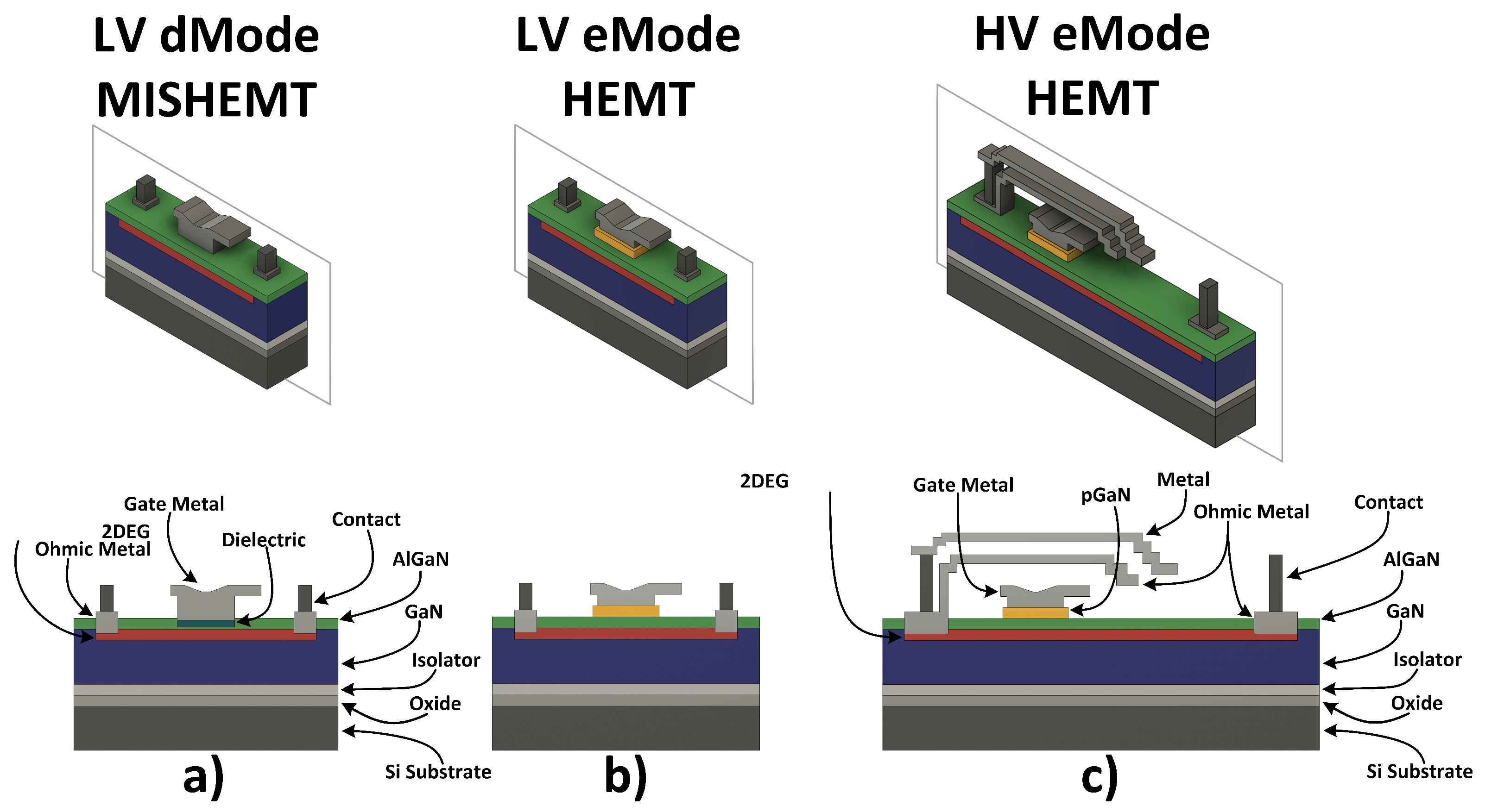
Figure 4.
HEMT model equivalent circuit
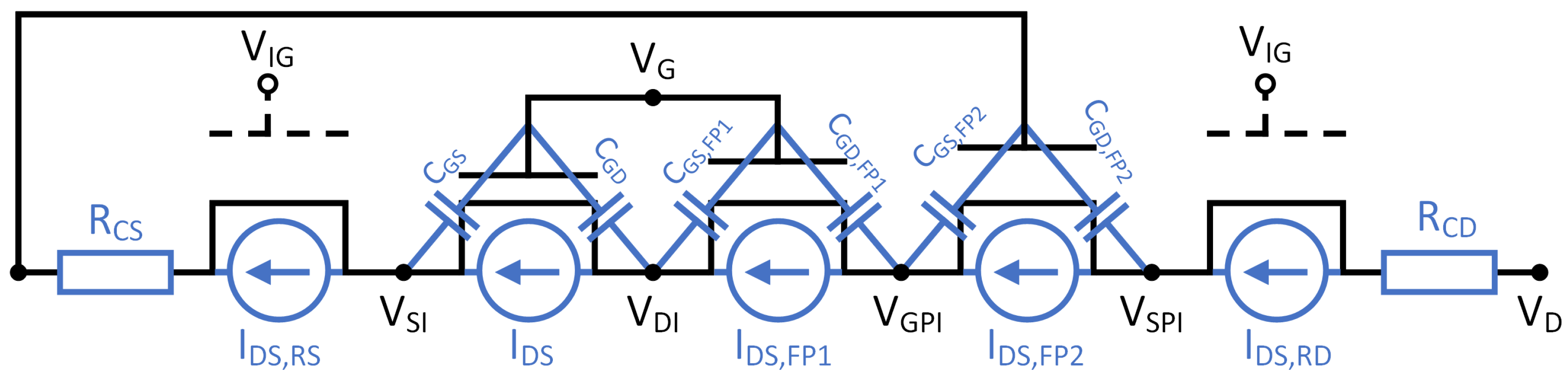
Figure 5.
GaN Inverters: a) RTL, b) DCFL, c) PCFL, and d1,d2) BS
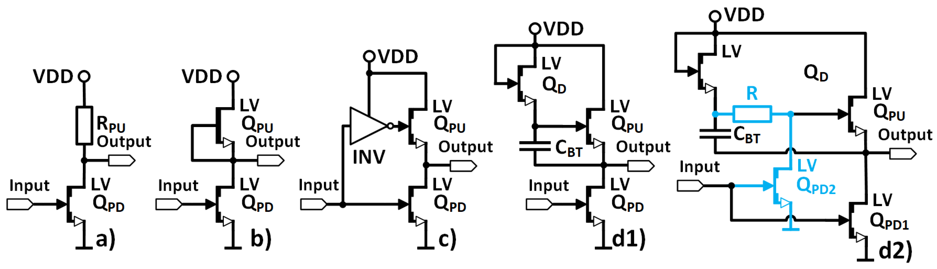

Table 1.
Semiconductors properties
| Material | k | |||||
| Si | 1.12 | 11.7 | 1350 | 0.3 | 1.5 | |
| GaAs | 1.42 | 12.9 | 8500 | 0.4 | 0.5 | |
| 4H-SiC | 3.23 | 9.66 | 900 | 2.5 | 4.9 | |
| GaN | 3.39 | 8.9 | 1265* | 3.75 | 1.3 | |
| 4.9 | 10 | 300 | 8 | 0.23** | ||
| Diamond | 5.47 | 5.7 | 4500 | 10 | 24 | |
| AlN | 6.1 | 8.5 | 500 | 15.9 | 3.21 | |
| Notes: *1265 in bulk, 2000 in 2DEG | ||||||
| **0.23 for [010] and 0.13 for [100] | ||||||
Table 2.
Devices Comparison
| Work | [23](V) | [22](V) | [27](L) | [28](L) | [29](L) | |
|---|---|---|---|---|---|---|
| Param. | ||||||
| Fin | CAVET | HEMT | HEMT | MIS-HEMT | ||
| GaN | GaN | Si | SiC | SiC | ||
| 1 | -2.8 | 0.64 | 1.8 | 3 | ||
| 0.2 | 16.2 | 9 | 0.62 | 0.8 | ||
| 1200 | 201 | 1200 | 1000 | 420 | ||
| 25 | 1.08 | 0.18 | 0.35 | 0.86 | ||
| Notes: L-Lateral, V-Vertical,* for V, for L | ||||||
Table 3.
Drivers Comparison
| Work | [54] | [55] | [56] | [49,57] | [51] | [52] | [53] | |
|---|---|---|---|---|---|---|---|---|
| Param. | ||||||||
| 5 | 12(1) | 6 | 6(2) | 12 | 24(4) | 5 | ||
| 25 | 5 | 10 | 6.25 | 3 | 1.2 | 10 | ||
| 2 | - | 4.75 | 6.6 | 10.2 | - | - | ||
| BS | RTL | RTL | RTL, PCFL | BS | CMOS | CMOS | ||
| 30 | 80 | - | 500 | 14.5(3) | 100 | 4.4 | ||
| 30 | 80 | 67 | 500 | 14.5(3) | 100 | 4.4 | ||
| 1.5 | 3 | 10 | - | 15 | 9 | 35 | ||
| 25 | 200 | 100 | 650 | 60 | 28 | 90 | ||
| 100 | - | - | - | 21 | 60(5) | 22.5 | ||
| ≈200@25 | - | 2070@10 | 132@30 | 40@3 | - | 75@0.5 | ||
| Notes: | ||||||||
| (1) is 6.8V and is 12V. (2) is 6V and is 11V. | ||||||||
| (3) In the previous datasheet version the value was 8.5. | ||||||||
| (4) The voltage gets internally regulated down to 5V. | ||||||||
| (5) The type of power consumption isn’t specified. Static power is assumed. | ||||||||
Disclaimer/Publisher’s Note: The statements, opinions and data contained in all publications are solely those of the individual author(s) and contributor(s) and not of MDPI and/or the editor(s). MDPI and/or the editor(s) disclaim responsibility for any injury to people or property resulting from any ideas, methods, instructions or products referred to in the content. |
© 2025 by the authors. Licensee MDPI, Basel, Switzerland. This article is an open access article distributed under the terms and conditions of the Creative Commons Attribution (CC BY) license (http://creativecommons.org/licenses/by/4.0/).
Copyright: This open access article is published under a Creative Commons CC BY 4.0 license, which permit the free download, distribution, and reuse, provided that the author and preprint are cited in any reuse.


