Submitted:
27 May 2025
Posted:
29 May 2025
You are already at the latest version
Abstract
To enhance thermal management efficiency of domestic SiC power semiconductor devices under high heat density, a multi-parameter co-optimization model based on an improved genetic algorithm is proposed. This model integrates thermal-structural-fluid coupling among package structure, heat dissipation interface, and cooling system. A multi-objective fitness function, combined with the NSGA-II algorithm, minimizes thermal resistance, junction temperature, and response time. Based on thermal network modeling, structure simplification and parameter extraction are performed. Experimental validation shows the optimized system significantly reduces steady-state junction temperature and response delay, enhancing dynamic adaptability and thermal safety, with strong potential for engineering applications.
Keywords:
SiC devices
; thermal management optimization
; improved genetic algorithm
; multi-objective co-design
1. Introduction
With advances in wide-bandgap semiconductor technology, SiC devices have become essential for high-density power electronic systems due to their high voltage tolerance, fast switching, and excellent thermal conductivity. However, in high-power, high-frequency operation, severe thermal accumulation impacts device reliability and system stability. During the localization of SiC chips, thermal management optimization is challenged by structural complexity, parameter coupling, and variable boundary conditions arising from the co-design of packaging, heat dissipation, and cooling systems [1]. Developing thermally efficient, engineering-oriented, and system-level co-optimization strategies is thus critical to enhancing the performance and safety margins of domestic SiC devices.
2. Modeling of Thermal Characteristics of SiC Power Semiconductors
2.1. Thermal Network Topology Construction
In modeling the thermal characteristics of SiC power semiconductor devices, constructing the thermal network topology is essential for accurately representing heat conduction paths. Using the thermal-electrical analogy, each conduction unit is abstracted as an equivalent network of thermal resistance (R) and heat capacity (C), forming a multilayer heat flow model. This model includes the chip core, package, substrate, and heat dissipation interface, with nodes linked through equivalent thermal resistances in a series-parallel configuration. To enhance practicality, a simplified π-type network is adopted to balance thermal behavior complexity and real-time computation efficiency [2]. As shown in Figure 1, the equivalent thermal network illustrates how each resistance parameter is derived from material conductivity, geometry, and interface conditions, providing the physical basis for subsequent modeling and optimization.
2.2. Mathematical Model Derivation
On the basis of the thermal network topology, the dynamic thermal behavior model of SiC power semiconductor devices is established based on the thermal-electrical equivalence theory, and each thermal resistance and heat capacity unit is correspondingly transformed into a first-order RC network structure. Under the simplified condition without considering the non-uniformity of heat source distribution, the thermal response of each layer node can be expressed by the following heat transfer equation [3]:
Where Ci denotes the i-th heat capacity, Ri is the thermal resistance between neighboring nodes, Ti(t) is the i-th node temperature, and P(t) is the power consumption per unit time.The thermal response model in a multi-node network can be unified into the following matrix form:
Where C, R, T(t) are the heat capacity matrix, thermal resistance matrix and temperature vector, respectively, which are suitable for multilayer structures to solve the thermal distribution state.
2.3. Model Simplification and Parameter Extraction
In order to improve the practicality and computational efficiency of the model in the engineering environment, the multi-node thermal network needs to be simplified moderately. Considering that the package shell structure with heat capacity much smaller than that of the chip area can be approximated as a steady-state heat transfer process, the corresponding RC branches in the network are simplified, and the dominant nodes of thermal resistance on the main heat transfer path are retained. The model further adopts the thermal resistance equivalent merging method to merge the units with smaller thermal resistance in the series structure to construct a three-layer node π-type thermal network structure. In the parameter extraction process, the thermal resistance Rth is calculated based on the following equation [4]:
where L is the length of the heat conduction path, λ is the thermal conductivity of the material, A is the cross-sectional area; and the heat capacity, C, is determined as follows:
where ρ is the material density, specific heat capacity cp, and volume V. Table 1 lists the thermal properties and corresponding geometrical dimensions of typical structural layers as a basis for subsequent thermal network parameterization.
3. Improved Genetic Algorithm Design
3.1. Question Coding Design
Due to the diversity of variables and complex constraints in the SiC power semiconductor thermal management optimization problem, traditional binary coding fails to meet the needs of continuous parameter precision and structural representation. This study adopts floating-point real number coding, mapping key design parameters—such as thermal resistance distribution, material thickness, and cooling structure size—sequentially to chromosomal loci, forming a real-number string of length n [5]. The coding sequence aligns with the heat flow path to maintain parameter logic and exclude physically invalid combinations. To improve the feasibility rate post-crossover, chromosome boundaries are normalized, and a validity check mechanism is embedded.
3.2. Adaptation Function Construction
To optimize key parameters in the SiC thermal management system, a multi-objective fitness function is constructed, targeting the minimum steady-state junction temperature, equivalent thermal resistance, and thermal response delay. The function incorporates normalized temperature terms and a constraint penalty mechanism. Let the optimization variables be X={x1,x2,...,xn}, with the fitness function defined as [6]:
where Tmax(X) is the peak junction temperature, Rth,eq(X) the main path thermal resistance, τ(X) the response time per unit power, and P(X) the penalty term for constraint violations. Weights w1,w2,w3 are empirically calibrated based on thermal design needs. This formulation balances thermal performance with structural constraints, ensuring search convergence within feasible boundaries [7]. Normalization enhances indicator comparability, while constraint filtering improves solution feasibility and search stability in the multi-parameter space.
3.3. Genetic Operator Improvement
To enhance convergence efficiency and maintain population diversity in thermal management optimization, several improvements are introduced to the genetic operators. For selection, a hybrid strategy combining Pareto sorting and double roulette is applied, with an elite retention rate of 20% to preserve top-performing individuals while ensuring cross-population coverage. The crossover operator employs an adaptive distribution-based crossover (SBX), with the crossover probability pc dynamically adjusted between 0.7 and 0.95 based on the generation count. This allows a balanced transition from global exploration to precise local search. The mutation operator uses a normal perturbation mechanism, where the mutation probability pm varies within [0.01, 0.15], and the perturbation amplitude is scaled by the current population’s variance. The mutation step is defined as:
where β=0.5 is the control coefficient and std(Xi) represents the standard deviation of the i-th variable. These operator designs together improve convergence quality and robustness across different optimization stages, without sacrificing diversity or feasibility [8].
4. Co-Optimization of Thermal Management Systems
4.1. Optimization Objective Analysis
The optimization targets system-level thermal performance, incorporating chip, package, and cooling interface layers. To ensure device reliability, the objective function minimizes steady-state junction temperature and total thermal resistance, while controlling dynamic response to enable rapid thermal fallback under power fluctuations [9]. Due to thermal-geometric-material coupling, variables such as encapsulation thickness and thermal conductivity impact diffusion rates, while cooling structure dimensions impose size and cost constraints. Thus, both thermal behavior and structural limits must be integrated into the objective system. Based on global conduction path analysis, steady-state metrics (temperature, resistance) and dynamic indicators (time constant) are weighted and combined, forming a constraint-aware optimization indicator set that guides collaborative design.
4.2. Optimization of Thermal Structure Parameters
This study redesigns the thermal conduction path from the SiC junction to the ambient by optimizing the geometry and materials of key layers. The base structure includes a 0.15 mm SiC chip, 0.10 mm SnAgCu solder, 0.38 mm AlN substrate, copper baseplate, 0.2 mm silicone grease TIM, and a 5.0 mm aluminum radiator. The optimization vector is defined as S=[L1,L2,A1,A2,N,H], where L1 and L2 are the thicknesses of the copper baseplate and radiator, A1 and A2 are the dissipation and contact areas, and NNN, HHH are the fin density and height, respectively. Constraints include a total vertical thickness under 8 mm and a 10 mm × 10 mm interface size. A thermal resistance model identifies dominant contributors to junction-to-ambient resistance. COMSOL simulations show that increasing L1 from 0.8 mm to 1.4 mm reduces solder-TIM interface temperature by 5.3 K at 100 W, while expanding A1 from 60 mm² to 120 mm² cuts lateral resistance by 22.5%. A fin density of 30 fins/cm² at 18 mm height improves convection without excessive pressure drop. After iterative optimization, the optimal set—L1=1.4, L2=4.5, A1=120mm², A2=180mm², N=30, H=18mm—achieves a 17.8% reduction in total thermal resistance and lowers peak junction temperature by 13.4 °C compared to the baseline.Figure 2 shows a schematic diagram of the packaging structure, heat dissipation interface, and cooling system.
4.3. Optimization of Cooling System Parameters
The optimization of cooling system parameters should focus on the dual objectives of cooling medium flow characteristics and heat exchange efficiency, with emphasis on the linkage control of key variables such as flow rate, inlet temperature, channel structure and interfacial heat transfer coefficient. By establishing the cooling system design parameter set C = {v, Tin, h, Dc}, the cooling flow rate v, flow channel diameter Dc and heat transfer coefficient h are included in the coupled optimization framework, and the empirical formula is used to construct the heat transfer evaluation index [10]:
Where Nu is the Nussell number and λ is the fluid thermal conductivity. Considering the influence of thermal-fluid impedance on the structure volume and power consumption, the microchannel structure and fluid guide plate are introduced in the optimized design to take into account the local forced convection and system flow resistance control.
4.4. Multi-Parameter Co-Optimization Strategy
The multi-parameter co-optimization strategy is based on the idea of coupled modeling, in which the heat dissipation structure parameter set S = {L1, A1, N} and the cooling system parameter set C = {v, h, Tin} are jointly constructed into the thermal-fluid-structural multi-dimensional optimization space. The unified expression of thermal response performance and structural constraints is realized by constructing the joint objective function:
where X contains all the design variables. In order to enhance the ability of capturing the nonlinear interactions among variables, NSGA-II, a multi-objective genetic algorithm based on Pareto front, is used, and an adaptive search guide factor is introduced to dynamically balance the convergence of junction temperature and flow resistance control. During the co-optimization process, all constraint mapping functions are uniformly normalized to enhance the search stability and convergence speed.
5. Experimental Validation and Result Analysis
5.1. Experimental Platform Construction
To validate the co-optimization strategy, a modular experimental platform was developed, integrating thermal load, multi-point sensing, and adaptive cooling control (Figure 3). It includes: (1)Thermal Load Module: A SiC MOSFET (Cree C3M0065090D) on a custom board driven by a programmable DC supply (Keysight N8957APV) generates heat fluxes from 50–150 W. (2)Sensing System: A 16-channel K-type thermocouple array (Omega TJ36-CAXL-116U-6) is embedded along the heat path with 0.5 mm resolution, and data are acquired at 1 MHz via NI PXIe-6368. (3)Cooling System: A microchannel cooler (Cooliance MD-01) with PWM-controlled pump and PID-regulated chiller (Julabo FP89) maintains flow rates (0.3–1.5 m/s) and temperatures (20–35 °C). (4)Control & Acquisition: LabVIEW 2023 manages real-time power, flow, and data logging. Infrared thermography (FLIR T1030sc) complements thermocouple readings, revealing surface temperatures and lateral heat spread.
5.2. Optimization Effect Analysis
(1) Steady-state performance: The co-optimized system was tested at power levels of 50 W, 100 W, and 150 W with coolant flow rates from 0.3 to 1.5 m/s. At 100 W and v=1.0m/s, the junction temperature Tj dropped to 108.7 °C, 10.5% lower than the baseline (121.4 °C). Thermal resistance Rth decreased by 21.7% (0.233 K/W vs. 0.298 K/W), as shown in Figure 4a,b. Infrared imaging revealed a more uniform temperature field and an 18.3% reduction in hotspot intensity. (2) Dynamic response: In transient tests (0→100 W in 10 ms), the thermal time constant τ dropped from 3.82 s to 2.97 s at v=0.5 m/s (Table 2), owing to improved lateral heat spreading and lower interfacial resistance from TIM optimization. (3) Multi-scenario validation: Tests under ambient temperatures of 25 °C, 35 °C, and 45 °C, and using water and 50% ethylene glycol as coolants, showed the optimized system maintained Tj<125 °C under all conditions (Figure 4). The use of glycol introduced a thermal resistance penalty of ≤8%, confirming design compatibility with industrial-grade coolants.
6. Conclusions
This study addresses thermal management challenges of SiC power semiconductor devices by establishing a multilevel thermal network model and applying an improved genetic algorithm to form a complete loop from modeling to experimental validation. Key innovations include: (1) constructing a multi-dimensional optimization space integrating structure, material, and cooling parameters; (2) employing a multi-objective fitness function with the NSGA-II algorithm to enhance convergence quality; and (3) building a real-condition experimental platform for model validation. However, the current strategy does not account for dynamic effects such as thermal fatigue and long-term stability. Future work may incorporate multi-physics coupling and reinforcement learning to improve adaptability under extreme thermal conditions, supporting broader applications in new energy vehicles, power systems, and other high-power-density fields.
References
- Pourfattah, F.; Sabzpooshani, M. On the thermal management of a power electronics system: Optimization of the cooling system using genetic algorithm and response surface method[J]. Energy 2021, 232, 120951. [Google Scholar] [CrossRef]
- Rafin, S.M.S.H.; Ahmed, R.; Haque, M.A.; et al. Power electronics revolutionized: A comprehensive analysis of emerging wide and ultrawide bandgap devices[J]. Micromachines 2023, 14, 2045. [Google Scholar] [CrossRef] [PubMed]
- Elqady, H.I.; El-Shazly, A.H.; Elkady, M.F. Parametric study for optimizing double-layer microchannel heat sink for solar panel thermal management[J]. Scientific Reports 2022, 12, 18278. [Google Scholar] [CrossRef] [PubMed]
- Kelly, B.J. DIGITAL CODESIGN OF A POWER MODULE WITH INTEGRATED THERMAL MANAGEMENT[D]. Georgia Institute of Technology, 2022.
- Hinov, N. Smart Energy Systems Based on Next-Generation Power Electronic Devices[J]. Technologies 2024, 12, 78. [Google Scholar] [CrossRef]
- Rajamony, R.; Wang, S.; Calderon-Lopez, G.; et al. Artificial neural networks-based multi-objective design methodology for wide-bandgap power electronics converters[J]. IEEE Open Journal of Power Electronics 2022, 3, 599–610. [Google Scholar] [CrossRef]
- Sun, L.; Qiao, M.; Xia, Y.; et al. Review of Voltage Balancing Techniques for Series-Connected SiC Metal–Oxide–Semiconductor Field-Effect Transistors[J]. Energies 2024, 17, 5846. [Google Scholar] [CrossRef]
- Tirupati Rao, V.; Raja Sekhar, Y. Hybrid photovoltaic/thermal (PVT) collector systems with different absorber configurations for thermal management–a review[J]. Energy & Environment 2023, 34, 690–735. [Google Scholar]
- Aouichak, I.; Jacques, S.; Bissey, S.; et al. A bidirectional grid-connected DC–AC converter for autonomous and intelligent electricity storage in the residential sector[J]. Energies 2022, 15, 1194. [Google Scholar] [CrossRef]
- Popescu, M.; Bitoleanu, A.; Suru, C.V.; et al. Shunt active power filters in three-phase, three-wire systems: A topical review[J]. Energies 2024, 17, 2867. [Google Scholar] [CrossRef]
Figure 1.
Equivalent topology of SiC power semiconductor thermal network.
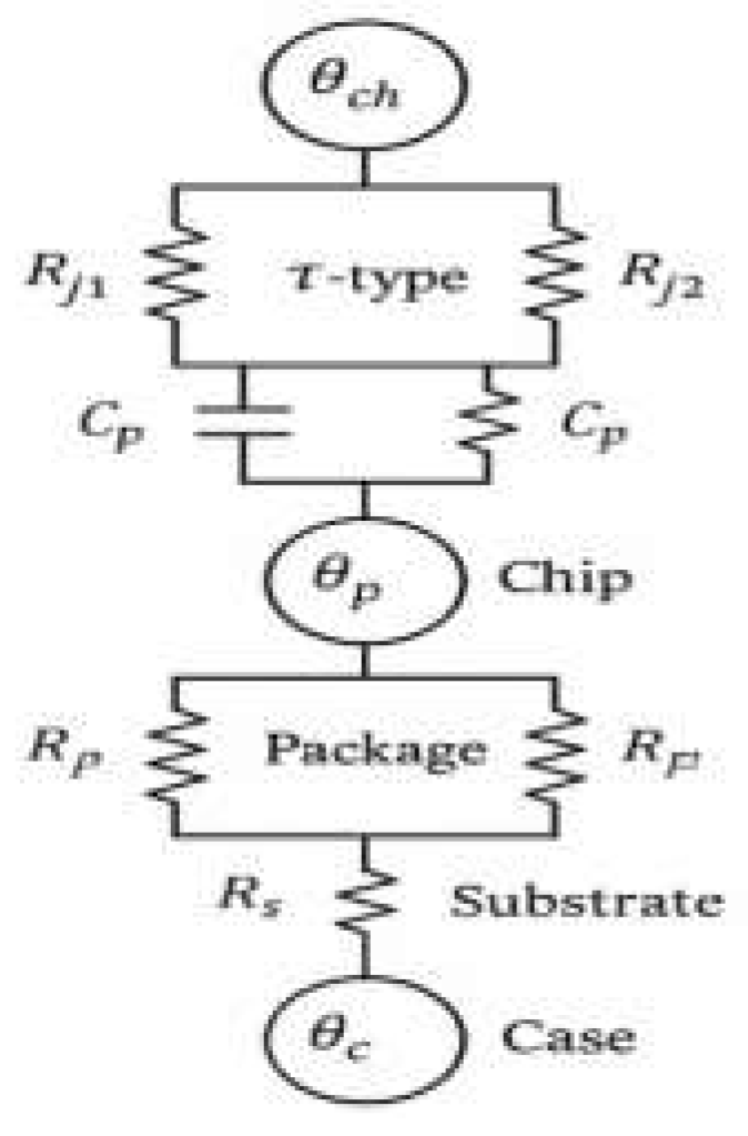
Figure 2.
Illustration of Package Structure, Heat Dissipation Interface, and Cooling System
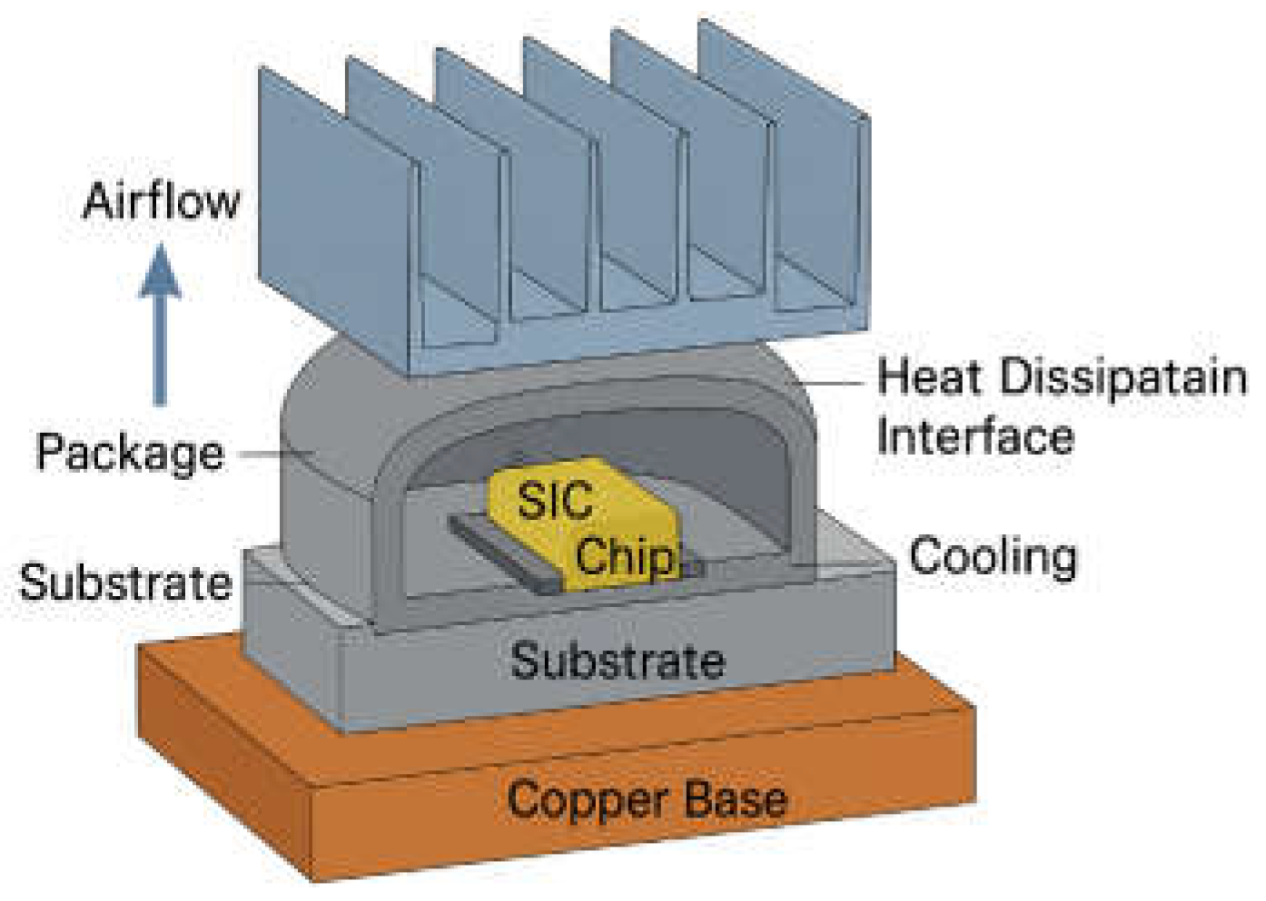
Figure 3.
Experimental platform composition and signal acquisition flowchart
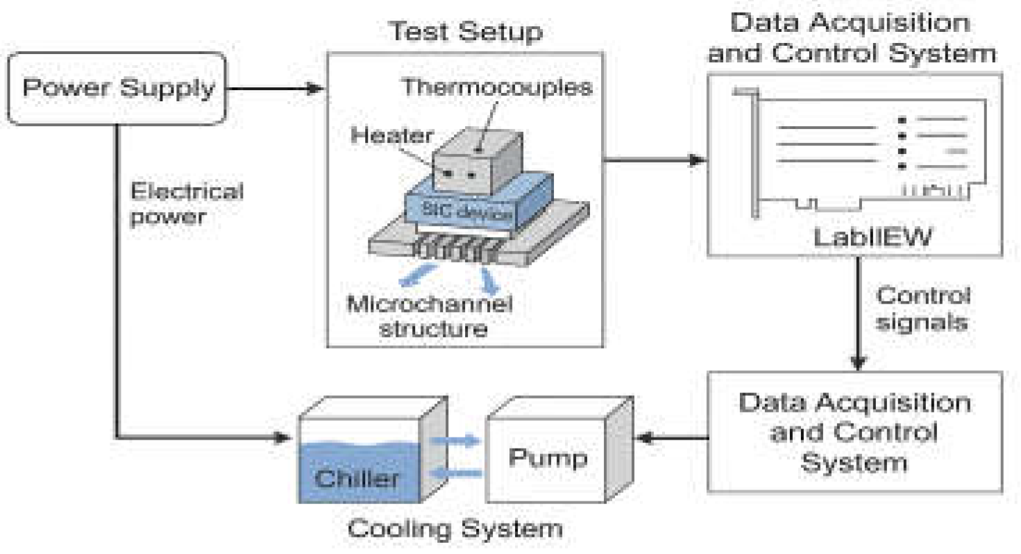
Figure 4.
(a) Junction temperature reduction at 100 W; (b) Thermal resistance vs. flow rate.
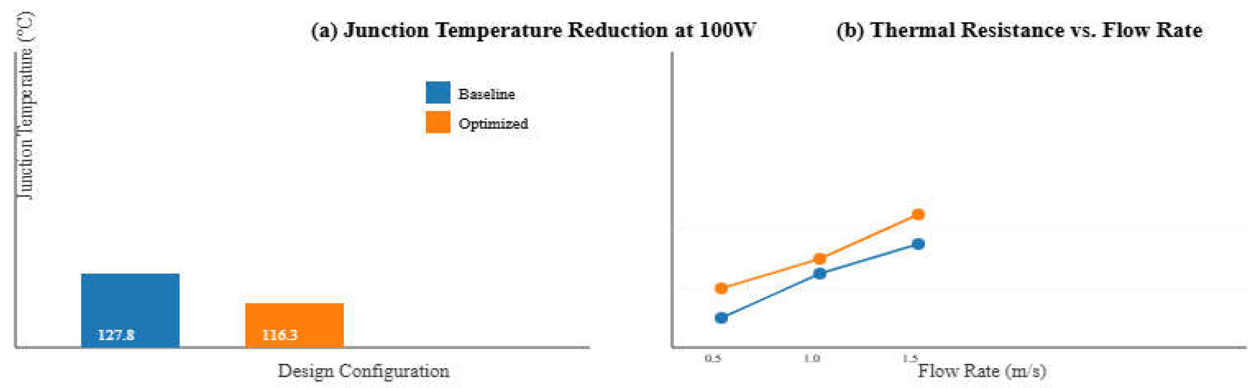
Figure 5.
Infrared images showing reduced hotspot intensity in the optimized design (left: baseline; right: optimized)
Figure 5.
Infrared images showing reduced hotspot intensity in the optimized design (left: baseline; right: optimized)
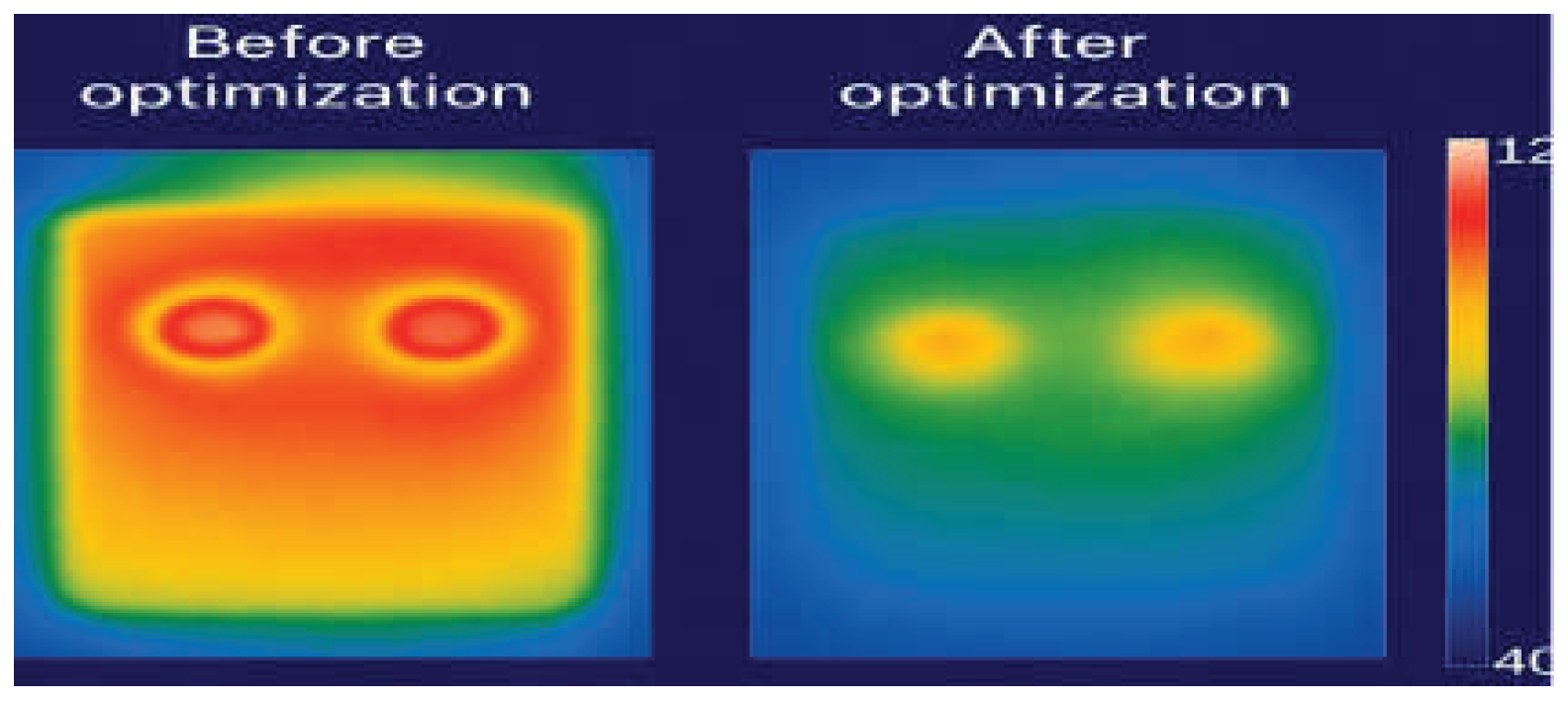

Table 1.
Thermal parameters and geometric properties of each structural layer
| structural layer | makings | Thermal conductivity λ(W/m-K) | Density ρ (kg/m³) | Specific heat capacity cp(J/kg-K) | Thickness L(mm) | Cross-sectional area A (mm²) |
| Chip (SiC) | SiC | 370 | 3210 | 690 | 0.15 | 1.5 × 1.5 = 2.25 |
| solder layer | SnAgCu | 50 | 7400 | 230 | 0.10 | 2.25 |
| DBC Ceramic Layer | AlN | 180 | 3300 | 740 | 0.38 | 2.25 |
| Copper Substrate (Heat Dissipation) | Cu | 390 | 8960 | 385 | 1.00 | 10.0 × 10.0 = 100.00 |
| TIM Thermally Conductive Interface Material | silicone grease | 5.5 | 2200 | 1300 | 0.20 | 100.00 |
| Radiator base plate | aluminum (chemistry) | 205 | 2700 | 900 | 5.00 | 100.00 |
TABLE 2.
THERMAL PERFORMANCE COMPARISON UNDER MULTIPLE FLOW RATES
| Flow Rate (m/s) | State | Tj,max (°C) | Rth,eq (K/W) | τ90% (s) |
| 0.5 | Baseline | 127.8 | 0.336 | 3.82 |
| 0.5 | Optimized | 116.3 | 0.282 | 2.97 |
| 1.0 | Baseline | 121.4 | 0.298 | 3.12 |
| 1.0 | Optimized | 108.7 | 0.233 | 2.26 |
Disclaimer/Publisher’s Note: The statements, opinions and data contained in all publications are solely those of the individual author(s) and contributor(s) and not of MDPI and/or the editor(s). MDPI and/or the editor(s) disclaim responsibility for any injury to people or property resulting from any ideas, methods, instructions or products referred to in the content. |
© 2025 by the authors. Licensee MDPI, Basel, Switzerland. This article is an open access article distributed under the terms and conditions of the Creative Commons Attribution (CC BY) license (http://creativecommons.org/licenses/by/4.0/).
Copyright: This open access article is published under a Creative Commons CC BY 4.0 license, which permit the free download, distribution, and reuse, provided that the author and preprint are cited in any reuse.


