Submitted:
20 May 2025
Posted:
20 May 2025
You are already at the latest version
Abstract
In response to Industry 4.0, smart manufacturing with highly developed performances has become an interest of research topic being intensively discussed. To achieve smart manufacturing, it is required to develop an intelligent factory having smart machines. Therefore, advanced low-cost sensing technologies are essential for gathering data and utilizing it for effectively building a smart machine. Recently, various high performance microcontrollers capable of performing data acquisition have been developed for the application of internet of things (IoT). However, the data acquisitions of those microcon-trollers are limited to several volts only. Therefore, voltage attenuation is required, thus resulting in the problem of reducing the resolution of acquired signal. In this paper, a signal acquisition system (SAS) using the Raspberry Pi Pico (Pico) that can acquire a large voltage waveform is proposed. Based on the operation of amplitude division, a complete waveform can be reconstructed via the proposed SAS without reducing the resolution. The SAS consists of three components: a signal acquisition circuit dividing a large voltage waveform into several segmented waveforms, a Pico reconstructing the piecewise segmented waveforms, and a laptop recording and displaying the acquired waveform. Through simulation works and practical experiments, it has been demon-strated that a sinusoidal waveform with the amplitude of 10 V and driving frequency of 100 Hz could be well reconstructed. Compared with the method using an attenuated waveform, the amplitude division featured much smaller acquisition error. Future works are to reduce the error of the acquired waveform by compensating for the non-linearity of the circuit and to implement a real-time acquisition system.
Keywords:
Industry 4.0
; signal acquisition device
; Raspberry Pi Pico
; amplitude division
; IoT
; smart machine
1. Introduction
Industry 4.0 (I4.0) has become an interest of research topic being intensively discussed. It is expected that I4.0 would bring about an extreme impact on manufacturing industry [1, 2]. For guiding the development of I4.0, the performance evaluation architecture has been divided into 5C levels, i.e., ‘Connection Level’, ‘Conversion Level’, ‘Cyber Level’, ‘Cognition Level’, and ‘Configuration Level’ [3]. I4.0-based smart manufacturing with highly developed performances can accurately predict product requirements and quickly identify errors, thus improving manufacturing processes and ultimately innovating products and services [4]. However, one of the most important factors to achieve smart manufacturing is to develop an intelligent factory having various smart machines. Therefore, advanced low-cost sensor technologies are essential for gathering data and utilizing it for effectively building a smart machine [5]. With the physical data acquired from sensors, smart manufacturing through machine learning, big data analysis, internet of things (IoT), and digital twin can be developed [6], in addition, the total manufacturing quality system based on decision support by combining sensor network data and historical data can be designed and realized [7, 8]. Therefore, the smart machine requires the most fundamental components of sensors to acquire manufacturing information such that an intelligent decision can be made based on big data analysis.
Recently, various versions of low-cost microcontrollers capable of performing data acquisition have been developed for the application of IoT, e.g., Arduino UNO and Micro [9], ESP32 and ESP8266 [10], and Raspberry Pi [11], etc. Among those microcontrollers, since the Raspberry Pi features further internet function, it has been widely used in numerous applications, e.g., development of a portable endoscopic 3-dimensional measurement system [12], implementation of data acquisition systems for powered vehicles [13, 14], parametric operations and monitoring of electrical parameters in photovoltaic power plants [15, 16, 17, 18], fault diagnosis and tool monitoring in manufacturing [19, 20, 21, 22, 23, 24, 25], construction of a predictive maintenance mechanism with the test platform and data analysis [26], temperature monitoring and thermal compensations in electrical components and machine tools [27, 28, 29, 30], development of electrical tomography system [31], implement of cloud platform for real-time data acquisition for a legacy machine [32], and development of monitoring systems with the integration of Raspberry Pi cluster and environmental sensor [33], etc. In 2021, a new version of Raspberry Pi Pico (for simplicity, Pico is used afterwards) was developed with additional inputs of analog-to-digital converters (ADCs) [34]. Regarding the performance, the clock speed of Pico behaves faster compared with that of Arduino UNO [35].
However, although those microcontrollers feature low-cost and powerful performances, the analog signal acquisitions via either an embedded or external ADC are limited to several volts only. Therefore, voltage attenuation using operational amplifiers (OPAs) [36] or voltage divider is required [37, 38]. Unfortunately, the voltage attenuation would result in the problem of reducing the small signal component to a level that is outside the resolution of the ADC [39]. In this paper, a signal acquisition system (SAS) using the Pico that can acquire a large voltage of 10 V with both positive and negative polarities is proposed. Based on the operation of amplitude division, a complete voltage waveform can be reconstructed in the microcontroller, thus without losing small signal due to attenuation. In preliminary study, the function of the SAS was verified [40]; in this paper, detailed electronic composition, simulation works, and performance comparison with that using the voltage attenuation are presented.
In the next section, acquisition principle of the SAS is described. Then, detail implementation of the SAS is presented in section 3. This is followed by the simulation works and experimental verification provided in sections 4 and 5, respectively. Finally, a conclusion is given in section 6.
2. Acquisition Principle
Figure 1 shows the acquisition principle of the proposed SAS for a sinusoidal signal with a large amplitude. In the beginning, the input alternating current (AC) voltage waveform is rectified into the one having the positive polarity only. Then, a voltage divider is used to provide several reference voltages, i.e., the multiples of 3.3 V. In the next, the rectified voltage waveform is compared to the reference voltages for division. As a result, several segmented waveforms having the maximum amplitude of 3.3 V are obtained via subtracting the rectified waveform with the reference voltages. Therefore, the segmented waveforms can be precisely and fully sensed by the Pico. Finally, a program is implemented to reconstruct the large voltage waveform via arithmetic operation.
3. Implementation of Signal Acquisition System
According to the acquisition principle shown in Figure 1, the SAS using Pico is configured as shown in Figure 2, in which three main components are depicted, including a signal acquisition circuit, Pico, and a laptop. Detailed composition is described in this section.
3.1. Signal Acquisition Circuit
The main function of signal acquisition circuit is to divide the input large voltage waveform into several segmented waveforms that can be completely sensed by the Pico. As shown in Figure 2, various electronic elements are employed, including a power supply, precision rectifier, voltage divider, priority encoder, 4:1 multiplexer (MUX), differential amplifier, zener diode, and two comparators. Their functions are briefly described in the following sections.
3.1.1. Precision Rectifier
Figure 3 shows the constitution of the precision rectifier comprising two OPAs, two zener diodes, and three resistors [41]. The precision rectifier can precisely rectify the AC waveform into a positive voltage waveform. To keep a complete waveform, it is unnecessary to the eliminate the ripple voltage.
3.1.2. Voltage Divider
The voltage divider is consisted of four series connected 330 Ω resistors. With the direct current (DC) power supply VDC1 of 13 V, four reference voltages of 0, 3.3 V, 6.6 V, and 9.9 V are provided as shown in Figure 4.
3.1.3. Comparators
Two comparators made of OPAs are used in the circuit. As shown in Figure 2, the comparator I is to examine either positive or negative polarity of the voltage waveform. Then, the polarity information is sensed by the Pico via the No.1 general purpose input/output (GPIO 1) as a digital port. On the other hand, the comparator II are made of three OPAs such that the amplitude comparisons among three cases of larger than 3.3 V, 6.6 V, and 9.9 V can be conducted as shown in Figure 4, in which the first OPA is to produce a LOW signal for the priority encoder. Therefore, including the case of 3.3 V, four ranges of segmented waveforms can be identified, i.e., 3.3 V, 3.3 – 6.6 V, 6.6 – 9.9 V, and > 9.9 V. The output digital signals noted with Ij (j = 0 to 3) are sent to the priority encoder for recording four voltage ranges.
3.1.4. Priority Encoder
Having identified four segmented waveforms via the compotator II, a 4:2 priority encoder is used to receive the information, and output 2-bit digital signals with 22 combinations, as shown in Figure 5, for the GPIO 2 & 3 to retrieve. Compared with the usual encoder that allows only one High level input, the priority encoder has a unique function to deal with some inputs having the same High level signal. That is because of the comparator II would produce multiple High signals when the voltage amplitude is larger than 3.3 V. The True table of the priority encoder is shown in Figure 5, in which X denotes “don’t care”.

Table 1.
True table of a 4:2 priority encoder.
| Input | Output | ||||
| I3 | I2 | I1 | I0 | O1 | O0 |
| X | X | X | 0 | 0 | 0 |
| X | X | 0 | 1 | 0 | 1 |
| X | 0 | 1 | 1 | 1 | 0 |
| 0 | 1 | 1 | 1 | 1 | 1 |
3.1.5. Multiplexor and Differential Amplifier
After assigning the information of four segmented waveforms to the encoder, the 4:1 multiplexor is used to select one of the reference voltages , i.e., 0, 3.3 V, 6.6 V, and 9.9 V for the differential amplitude to subtract. Therefore, an input large voltage waveform can be divided into four segmented waveforms with the maximum amplitude of 3.3 V that can be sensed by the Pico. A zener diode is used to limit the input voltage being under 3.3 V for protecting the Pico. The constitution of the differential amplitude is shown in Figure 6. The output segmented waveforms obtained with the amplitude division are expressed as follows,
3.2. Raspberry Pi Pico
Pico is a microcomputer chip equipped with various components such as digital input and output (I/O) ports, memory, and networking element, etc. It has been widely employed in automation machinery. With the analog input function of ADCs, the main specifications of Pico are listed in Table 2.
3.2.1. GPIO
As shown in Figure 2, the GPIO 1 is used to record the polarity of waveform, whereas the GPIO 2 & 3 are used to store the reference voltages of segmented waveforms. The True table of the GPIO ports are expressed in Table 2.
Table 2.
True tables of the GPIO 1 ~ 3 ports.
| GPIO | GPIO | ||||
| 1 | Polarity | 2 | 3 | (V) | |
| 0 | Positive | 0 | 0 | 0 | |
| 1 | Negative | 0 | 1 | 3.3 | |
| 1 | 0 | 6.6 | |||
| 1 | 1 | 9.9 | |||
3.2.2. ADC
The segmented waveforms having the maximum amplitude of 3.3 V are acquired via the ADC port. Since the resolution of ADC of Pico is 12-bit, the acquired voltage signal is with the resolution of 0.81 mV (= 3.3/212 V). However, because the program is implemented by the MicroPython which defines the resolution of ADC be 16-bit, the acquired segmented waveform is expressed as follows,
where is the sensed segmented waveform of ADC.
3.2.2. Waveform Reconstruction Program
Having obtained the information of polarity, reference voltage , and sensed segmented waveform , a complete waveform is reconstructed via the implemented program with the flowchart shown in Figure 7. In the beginning, the reference voltage is selected based on the GPIO signals, then the value of is added to the segmented waveform, as a result, the complete waveform can be obtained and stored into a text file. Finally, a full voltage waveform can be displayed on the laptop via graphical package.
The algorithm of selecting the reference voltage is shown in Figure 8. Firstly, the positive polarity is checked based on the GPIO 1 signal, then the reference voltage larger than 3.3 V, 6.6 V, or 9.9 V is sequentially examined according to the signals of GPIO 2&3. As a result of the examinations, one of the positive reference voltages, i.e., 0, 3.3 V, 6.6 V, and 9.9 V, can be determined. On the other hand, when the negative polarity is checked, similar to previous processes, one of the negative reference voltages can be determined. From the flowchart, it is noted that the larger the reference voltage is, the longer is the examining process. In addition, the positive polarity has a shorter examining process compared to the negative one for the same value. Figure 9 shows the screen copies of program executions for (a) an acquisition example of ADC, indicating the acquired readings of ranging 0 ~ 65535 due to the MicroPython resolution of 16-bit, and (b) part of waveform reconstruction program based on flowchart of Figure 7.
4. Simulation Works
According to the configuration shown in Figure 2, the simulation works were performed using the simulation program with integrated circuit emphasis (SPICE) package. The acquired data include a complete waveform, segmented waveforms, reference voltages, and polarity signal.
4.1. Simulation Waveforms and Signals
Figure 10 shows the simulation results for a sinusoidal waveform with an amplitude of 10 V and a frequency of 0.5 Hz. The numerical probes were placed on the outputs of rectifier P1, comparator I P2, MUX P3, and zener diode P4, as shown in Figure 2. Firstly, the rectifier flipped the negative voltage waveform into the positive one, and the comparator I provided the step signal showing the positive and negative polarities. Then the MUX selected the reference voltages expressed by stepwise signals, and the differential amplifiers outputted the piecewise segmented waveforms with the maximum amplitude of 3.3 V kept by the zener diode. Finally, the full waveform S1 having both the positive and negative polarities was completely reconstructed via the algorithm presented in Figure 7.
4.2. Simylation Waveform Affected by Frequency
By applying two different frequencies of 1 Hz and 100 Hz to the simulation circuit, the reconstructed waveforms and calculated errors are shown in Figure 11. From the results, although two waveforms could be smoothly reconstructed, errors with various spikes were found. Notably, large spike peaks of −0.2 V and 0.1 V appeared at the crossovers of polarity change for 1 Hz and 100 Hz, respectively. Figure 12 shows the peak-to-valley (PV) error affected by the actuating frequency. When the driving frequency was under 100 Hz, the PV error was with the similar value of 0.25 V, however, it significantly rose when the driving frequency was larger than 100 Hz.
5. Experimental Verification
Similar to the simulation works, experimental verification was performed with the implemented SAS. In addition to the same information obtained with the simulation works, acquisition time delay of ADC, and the signal acquisitions based on the SAS are compared with that using the attenuated waveforms based on a voltage divider.
5.1. Experimental Setup
Figure 13 shows the experimental setup for examining the proposed SAS. The DC power supply is used to provide constant voltages to the signal acquisition circuit, and a function generator is employed to produce the sinusoidal waveforms with various frequencies. An oscilloscope is provided to record the input waveform, segmented waveforms, reference voltages, and polarity signal. The Pico is used to acquire the segmented waveform, and to reconstruct the full waveform based on the GPIO digital signals. A laptop is employed to record the acquired data and present graphical display. Figure 14 is the photograph of experimental setup.
5.2. Measured Time Delay of ADC
To examine the time delay of signal acquisition, DC voltages were applied to the SAS. The time delay is referred to the time interval between the voltage is just sensed by the ADC port and then output a “print” command after computational process. Figure 15 shows the relation between the delay time vs. the amplitude with polarity of the voltage. The voltages were applied by the reference voltages, i.e., 0, 3.3 V, 6.6 V, and 9.9 V but with both positive and negative polarities. Every value was acquired 10 times for examining the repeatability. As shown in the figure, when the voltage is 0, it results in the average time delay of 93.1 μs; on the other hand, when the voltage is −9.9 V, it appears the largest time delay of 125 μs. That is, the sampling rate could reach 8,000 samples per second. Also, it is observed that the larger the amplitude is, the longer is the delay time; and the positive polarity behaves a shorter time delay for the same amplitude due to a higher calculation priority. This copes well with the algorithm of determining the reference voltage depicted in Figure 8.
5.3. Measured Results of Sinusoidal Waveform
Based on the implemented experimental setup, experiments were conducted. Similar to simulation works, the input waveform with a large amplitude was divided into several segmented waveforms with maximum amplitude of 3.3 V via the signal acquisition circuit, then the segmented waveforms were acquired with the Pico, and a complete waveform was reconstructed by the implemented program. In addition, the measured errors affected by frequency were examined.
5.3.1. Reconstruction Waveform and Measured Signals
Figure 16 shows the reconstructed waveform and measured signals for an input sinusoidal waveform with an amplitude of 10 V and a frequency of 0.5 Hz. The oscilloscope probes were placed on the outputs of rectifier P1, comparator I P2, MUX P3, and zener diode P4, as shown in Figure 2. The complete waveform S1 was reconstructed via the implemented program of Pico. Similar to the simulation results, P1 recorded the positive and rectified waveforms; P2 presented the step signal showing the positive and negative polarities; P3 showed the stepwise reference voltages; and P4 indicated the piecewise segmented waveforms. Finally, S1 demonstrated the reconstructed waveform. Therefore, the effective function of proposed SAS was experimentally demonstrated.
5.3.2. Reconstructed Waveform Affected by Frequency
In addition, by applying two sinusoidal waveforms with the frequencies of 1 Hz and 100 Hz to the signal acquisition circuit, the reconstructed waveforms and calculated errors are shown in Figure 17. From the results, it is shown that two waveforms could be smoothly reconstructed, and the error ranges were ranged in −0.2 ~ 0.1 V and −0.13 ~ 0.13 V for the frequencies of 1 Hz and 100 Hz, respectively. The PV error with the relation to the frequency is depicted in Figure 18. When the driving frequency was under 100 Hz, the PV error fluctuated within 0.27 ~ 0.34 V. However, it significantly increased to 0.95 V and 3.6 V when the frequencies were 500 Hz and 1 kHz, respectively.
5.4. Measured Results of Attenuated Sinusoidal Waveform
To further demonstrate the effectiveness of the proposed SAS, referring to the voltage attenuation based on voltage divider [37, 38], the sinusoidal waveforms with the amplitude of 10 V were attenuated to 3.3 V with the experimental configuration shown in Figure 19, where After acquiring the attenuated waveforms using the SAS, their amplitudes were amplified with the ratio of 10/3.3 for comparison consistency. As a result, the experimental results for the attenuated waveforms are shown in Figure 20. It can be seen that although both the waveforms having the frequencies of 1 Hz and 100 Hz could be smoothly reconstructed, their corresponding errors were with the similar range of −0.5 ~ 0.4 V, which were much worse than previous results without voltage attenuation. In addition, the PV error affected by the frequency is shown in Figure 21, when the driving frequency was under 100 Hz, the PV error nearly reached 1 V. When the frequency was 500 Hz, the PV error increased to 3 V. As a result of the examinations, the proposed SAS that features better accuracy compared to that using the voltage divider was demonstrated.
6. Conclusions
To overcome the weakness of acquisition ability of small voltage of a microcontroller, a signal acquisition system capable of acquiring a large voltage waveform based on low-cost Raspberry Pi Pico was proposed. The SAS was employed to divide the waveform having a large amplitude into several segmented waveforms that can be sensed by the Pico, and the full waveform was reconstructed via implemented program. Through simulation works and experimental examinations, the effectiveness of the SAS was demonstrated. Main results are drawn as follows,
- (1)
- The simulation results based on SPICE showed that a sinusoidal waveform with a large amplitude could be sensed and smoothly reconstructed. When the frequency was under 100 Hz, the PV error was with the value of 0.25 V.
- (2)
- The DC voltages were applied to examine the time delay of voltage acquisition. When the voltage was 0, the average time delay was 93.1 μs; when the voltage was −9.9 V, the SAS appeared the largest time delay of 125 μs. That is, the sampling rate could reach 8,000 samples per second.
- (3)
- The experimental results based on SAS showed that a sinusoidal waveform with a large amplitude could be sensed and smoothly reconstructed. When the frequency was under 100 Hz, the PV error fluctuated within 0.27 ~ 0.34 V.
- (4)
- The experiments for the attenuated waveform based on the voltage divider were conducted. Although the waveforms could be smoothly reconstructed, the PV error ranging −0.5 ~ 0.4 V showed much worse acquisition accuracy than that without voltage attenuation.
Future works are to improve the acquisition accuracy by compensating for the nonlinearity of the acquisition circuit and implementing a device with on-line acquisition function.
Funding
Financial support from the National Science and Technology Council of the Republic of China (Taiwan) with grant No. NSTC 113-2221-E-992-035- is gratefully acknowledged.
Conflicts of Interest
The authors declare no conflicts of interest.
Abbreviations
The following abbreviations are used in this manuscript:
| AC | Alternating current |
| ADC | Analog-to-digital converter |
| DC | Direct current |
| GPIO | General purpose input/output |
| I4.0 | Industry 4.0 |
| IoT | Internet of things |
| MUX | Multiplexor |
| OPA | Operational amplifier |
| SAS | Signal acquisition system |
| SPICE | Simulation program with integrated circuit emphasis |
References
- Qin, J.; Liu, Y.; Grosvenor, R. A Categorical Framework of Manufacturing for Industry 4.0 and Beyond. Procedia CIRP 2016, 52, 173–178. [Google Scholar] [CrossRef]
- Abdullah, F.M.; Saleh, M.; Al-Ahmari, A.M.; Anwar, S. The Impact of Industry 4.0 Technologies on Manufacturing Strategies: Proposition of Technology-Integrated Selection. IEEE Access 2022, 10, 21574–21583. [Google Scholar] [CrossRef]
- Lee, J.; Bagheri, B.; Kao, H.-A. A Cyber-Physical Systems Architecture for Industry 4.0-Based Manufacturing Systems. Manufacturing Letters 2015, 3, 18–23. [Google Scholar] [CrossRef]
- Sahoo, S.; Lo, C.-T. Smart Manufacturing Powered by Recent Technological Advancements: A Review. Journal of Manufacturing Systems 2022, 64, 236–250. [Google Scholar] [CrossRef]
- Kalsoom, T.; Ramzan, N.; Ahmed, S.; Ur-Rehman, M. Advances in Sensor Technologies in the Era of Smart Factory and Industry 4.0. Sensors 2020, 20, 6783. [Google Scholar] [CrossRef]
- Kler, R.; Ashish; Nimmagadda, P.; Navarajan, J.; Chauhan, D.; Babu, G.R. Recognition and Implementation of the Smart Manufacturing Systems in Industrial Sectors for Evolving Industry 4.0. Measurement: Sensors 2024, 31, 100987. [Google Scholar] [CrossRef]
- Tanane, B.; Bentaha, M.-L.; Dafflon, B.; Moalla, N. Bridging the Gap between Industry 4.0 and Manufacturing SMEs: A Framework for an End-to-End Total Manufacturing Quality 4.0’s Implementation and Adoption. Journal of Industrial Information Integration 2025, 45, 100833. [Google Scholar] [CrossRef]
- Jaskó, S.; Ruppert, T. The Future of Manufacturing and Industry 4.0. Appl. Sci. 2025, 15, 4655. [Google Scholar] [CrossRef]
- Available online: https://docs.arduino.cc/hardware/ (accessed on 16 May 2025).
- Available online: https://www.espressif.com/en/products/socs (accessed on 16 May 2025).
- Available online: https://www.raspberrypi.com/products/ (accessed on 16 May 2025).
- Schlobohm, J.; Pösch, A.; Reithmeier, E. A Raspberry Pi Based Portable Endoscopic 3D Measurement System. Electronics 2016, 5, 43. [Google Scholar] [CrossRef]
- Ambrož, M. Raspberry Pi as a Low-Cost Data Acquisition System for Human Powered Vehicles. Measurement 2017, 100, 7–18. [Google Scholar] [CrossRef]
- Pérez-Zuriaga, A.M.; Llopis-Castelló, D.; Just-Martínez, V.; Fonseca-Cabrera, A.S.; Alonso-Troyano, C.; García, A. Implementation of a Low-Cost Data Acquisition System on an E-Scooter for Micromobility Research. Sensors 2022, 22, 8215. [Google Scholar] [CrossRef] [PubMed]
- Sukič, P. Štumberger, G. Intra-Minute Cloud Passing Forecasting Based on a Low Cost IoT Sensor—A Solution for Smoothing the Output Power of PV Power Plants. Sensors 2017, 17, 1116. [Google Scholar] [CrossRef]
- Pereira, R.I.S.; Dupont, I.M.; Carvalho, P.C.M.; Jucá, S.C.S. IoT Embedded Linux System Based on Raspberry Pi Applied to Real-Time Cloud Monitoring of a Decentralized Photovoltaic Plant. Measurement 2018, 114, 286–297. [Google Scholar] [CrossRef]
- González, I.; Portalo, J.M.; Calderón, A.J. Configurable IoT Open-Source Hardware and Software I-V Curve Tracer for Photovoltaic Generators. Sensors 2021, 21, 7650. [Google Scholar] [CrossRef]
- Adigüzel, E.; Gürkan, K.; Ersoy, A. Design and Development of Data Acquisition System (DAS) for Panel Characterization in PV Energy Systems. Measurement 2023, 221, 113425. [Google Scholar] [CrossRef]
- Lu, Y.-S.; Wang, H.-W.; Liu, S.-H. An Integrated Accelerometer for Dynamic Motion Systems. Measurement 2018, 125, 471–475. [Google Scholar] [CrossRef]
- Pham, M.T.; Kim, J.-M.; Kim, C.H. Deep Learning-Based Bearing Fault Diagnosis Method for Embedded Systems. Sensors 2020, 20, 6886. [Google Scholar] [CrossRef]
- Soto-Ocampo, C.R.; Mera, J.M.; Cano-Moreno, J.D.; Garcia-Bernardo, J.L. Low-Cost, High-Frequency, Data Acquisition System for Condition Monitoring of Rotating Machinery through Vibration Analysis-Case Study. Sensors 2020, 20, 3493. [Google Scholar] [CrossRef]
- Biglari, A.; Tang, W. A Review of Embedded Machine Learning Based on Hardware, Application, and Sensing Scheme. Sensors 2023, 23, 2131. [Google Scholar] [CrossRef]
- Tran, M.-Q.; Doan, H.-P.; Vu, V.Q.; Vu, L.T. Machine Learning and IoT-Based Approach for Tool Condition Monitoring: A Review and Future Prospects. Measurement 2023, 207, 112351. [Google Scholar] [CrossRef]
- Kodrič, M.; Korbar, J.; Pogačar, M.; Čepon, G. Development of a Resource-Efficient Real-Time Vibration-Based Tool Condition Monitoring System Using PVDF Accelerometers. Measurement 2025, 251, 117183. [Google Scholar] [CrossRef]
- Bhandarkar, V.V.; Das, B.; Tandon, P. Real-Time Remote Monitoring and Defect Detection in Smart Additive Manufacturing for Reduced Material Wastage. Measurement 2025, 252, 117362. [Google Scholar] [CrossRef]
- Chuang, S.-Y.; Sahoo, N.; Lin, H.-W.; Chang, Y.-H. Predictive Maintenance with Sensor Data Analytics on a Raspberry Pi-Based Experimental Platform. Sensors 2019, 19, 3884. [Google Scholar] [CrossRef] [PubMed]
- Kunicki, M.; Borucki, S.; Zmarzły, D.; Frymus, J. Data Acquisition System for On-Line Temperature Monitoring in Power Transformers. Measurement 2020, 161, 107909. [Google Scholar] [CrossRef]
- Kristiani, E.; Wang, L.-Y.; Liu, J.-C.; Huang, C.-K.; Wei, S.-J.; Yang, C.-T. An Intelligent Thermal Compensation System Using Edge Computing for Machine Tools. Sensors 2024, 24, 2531. [Google Scholar] [CrossRef]
- Li, J.; Pei, H.; Kochan, O.; Wang, C.; Kochan, R.; Ivanyshyn, A. Method for Correcting Error Due to Self-Heating of Resistance Temperature Detectors Suitable for Metrology in Industry 4.0. Sensors 2024, 24, 7991. [Google Scholar] [CrossRef]
- Iafolla, L.; Santoli, F.; Carluccio, R.; Chiappini, S.; Fiorenza, E.; Lefevre, C.; Loffredo, P.; Lucente, M.; Morbidini, A.; Pignatelli, A.; Chiappini, M. Temperature Compensation in High Accuracy Accelerometers Using Multi-Sensor and Machine Learning Methods. Measurement 2024, 226, 114090. [Google Scholar] [CrossRef]
- Zamora-Arellano, F.; López-Bonilla, O.R.; García-Guerrero, E.E.; Olguín-Tiznado, J.E.; Inzunza-González, E.; López-Mancilla, D.; Tlelo-Cuautle, E. Development of a Portable, Reliable and Low-Cost Electrical Impedance Tomography System Using an Embedded System. Electronics 2021, 10, 15. [Google Scholar] [CrossRef]
- Ho, M.-H.; Lai, M.-Y.; Liu, Y.-T. Implementation of DDS Cloud Platform for Real-Time Data Acquisition of Sensors for a Legacy Machine. Electronics 2022, 11, 2096. [Google Scholar] [CrossRef]
- Donca, I.-C.; Stan, O.P.; Misaros, M.; Stan, A.; Miclea, L. Comprehensive Security for IoT Devices with Kubernetes and Raspberry Pi Cluster. Electronics 2024, 13, 1613. [Google Scholar] [CrossRef]
- Available online: https://www.raspberrypi.com/products/raspberry-pi-pico/ (accessed on 16 May 2025).
- Thothadri, M. An Analysis on Clock Speeds in Raspberry Pi Pico and Arduino Uno Microcontrollers. American Journal of Engineering and Technology Management 2021, 6, 41–46. [Google Scholar] [CrossRef]
- Pete Wilson, P.E. High-Voltage Signal Conditioning for Low-Voltage ADCs. Application Report, SBOA097, Texas Instruments 2004.
- Aghenta, L.O.; Iqbal, M.T. Low-Cost, Open Source IoT-Based SCADA System Design Using Thinger.IO and ESP32 Thing. Electronics 2019, 8, 822. [Google Scholar] [CrossRef]
- Pauzan, M.; Yanti, I. Utilization of ADC Pin on Arduino Nano to Measure Voltage of a Battery. TEKNOKOM: Jurnal Teknologi dan Rekayasa Sistem Komputer 2021, 4, 66–72. [Google Scholar] [CrossRef]
- Patangia, H.C.; Gregory, D. High Voltage Signal Processing Using a Small Signal Approach. IEEE International Symposium on Signal Processing and Information Technology 2007, 1088-6. [Google Scholar] [CrossRef]
- Chen, L.-X.; Chang, K.-M.; Liu, Y.-T. Signal Acquisition Device for Large Voltage Waveform Using Low-cost Raspberry Pi Pico W. In Proceedings of the 27th International Conference on Mechatronics Technology (ICMT2024), Kanazawa, Japan, 11-19, 2024.
- Available online: https://www.eet-china.com/mp/a71275.html (accessed on 16 May 2025).
Figure 1.
Acquisition principle of the SAS.
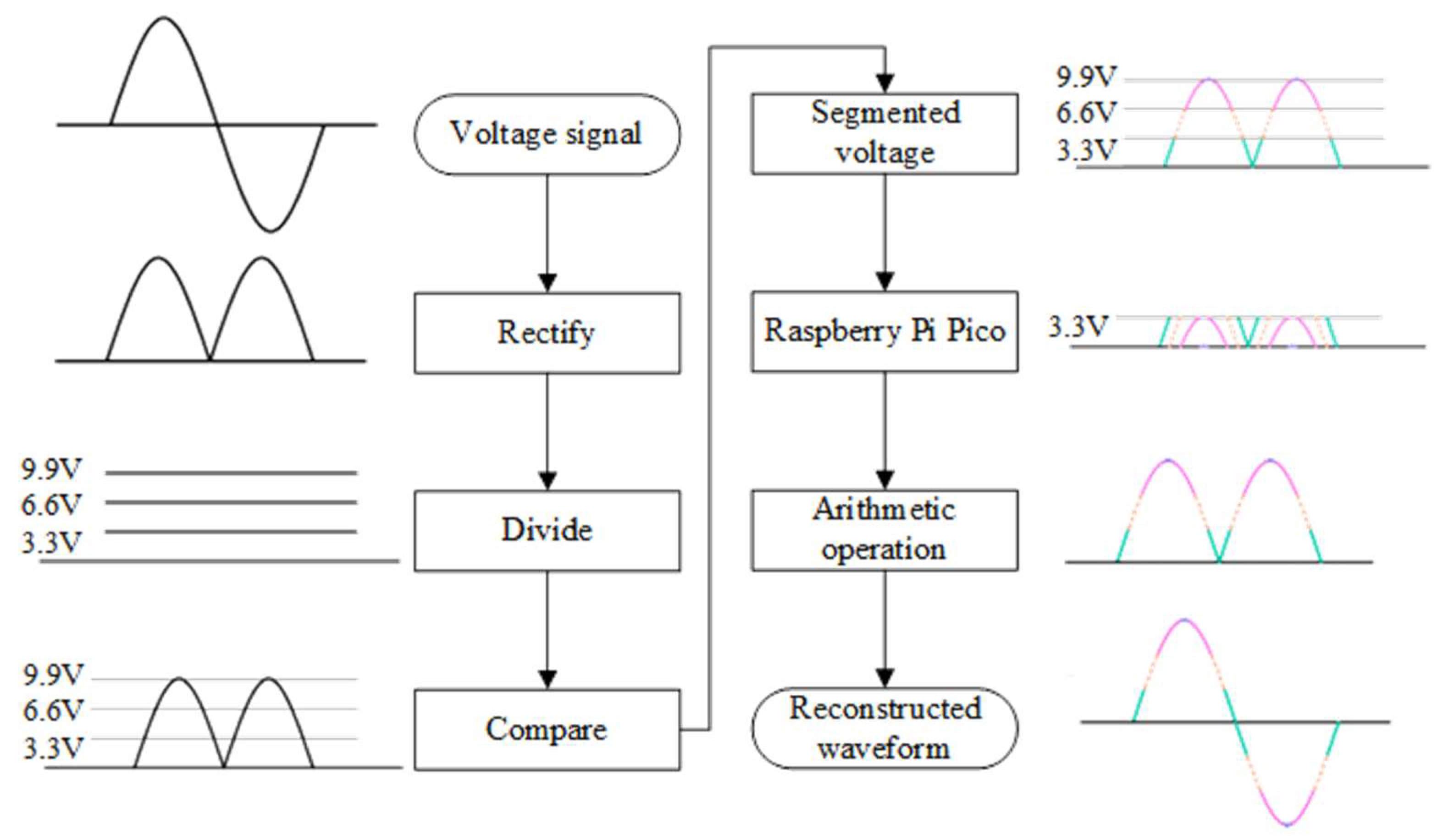
Figure 2.
Main components of the SAS.
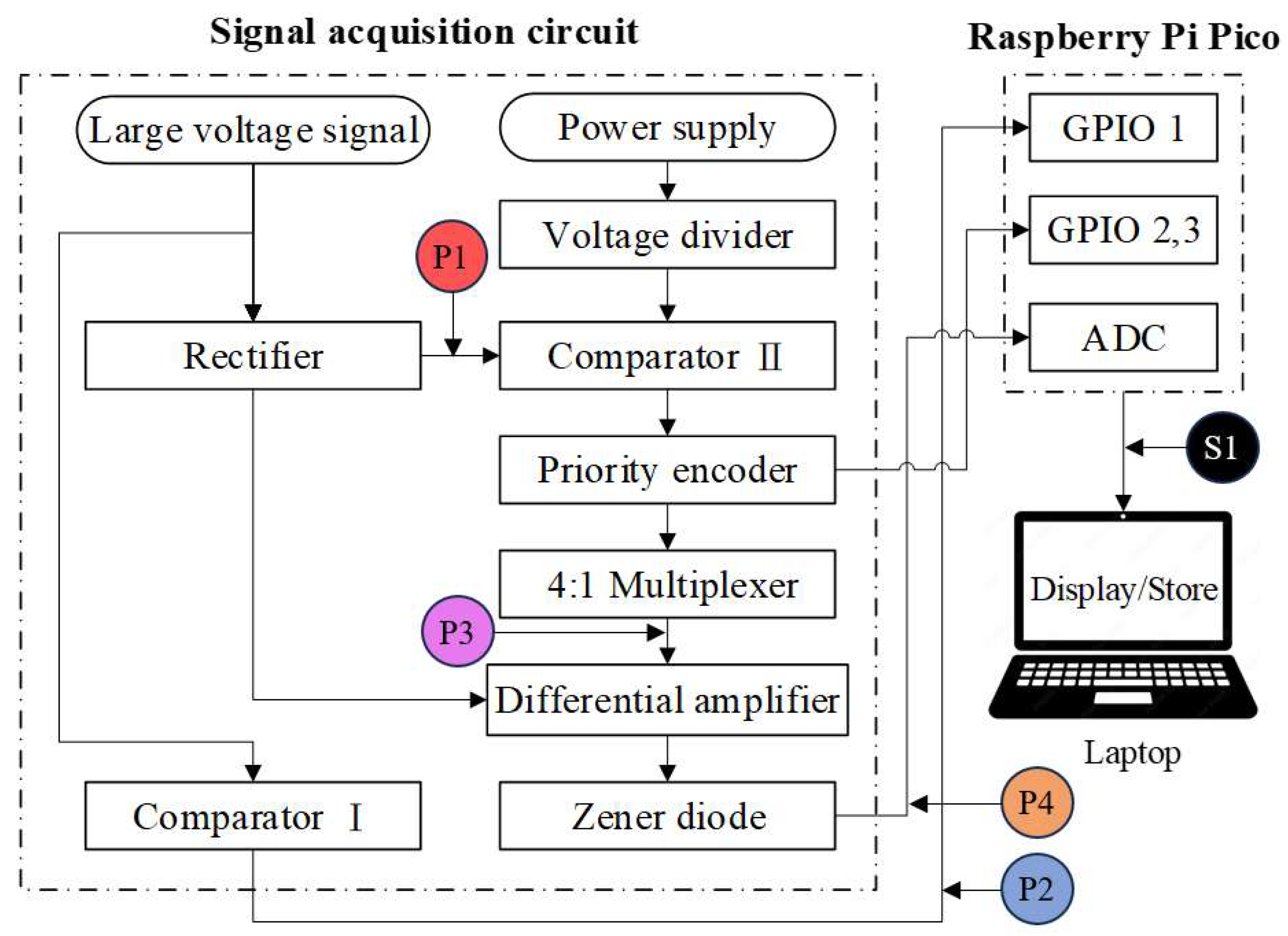
Figure 3.
The constitution of a precision rectifier.
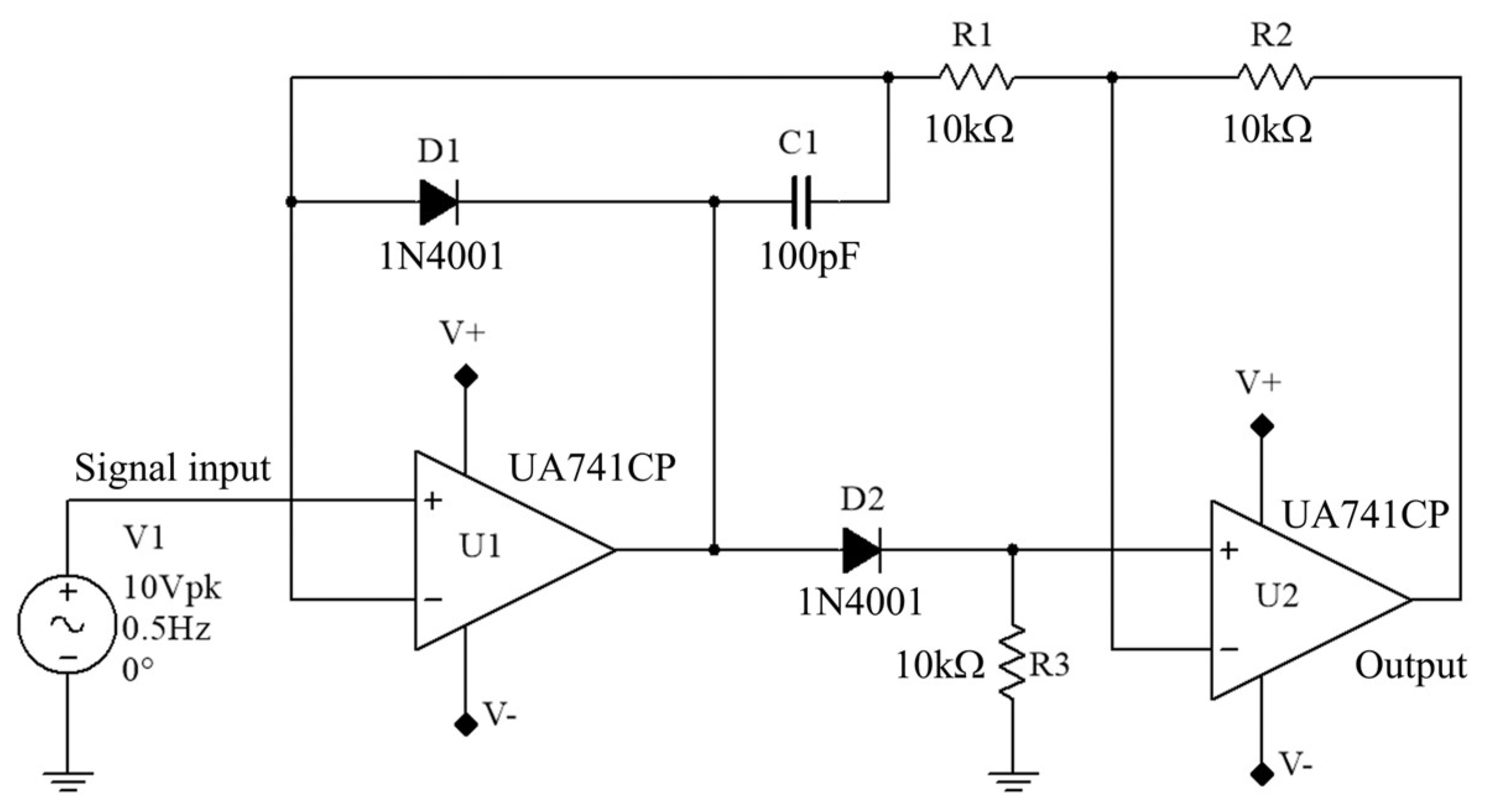
Figure 4.
The voltage divider with four reference voltages for comparator II.
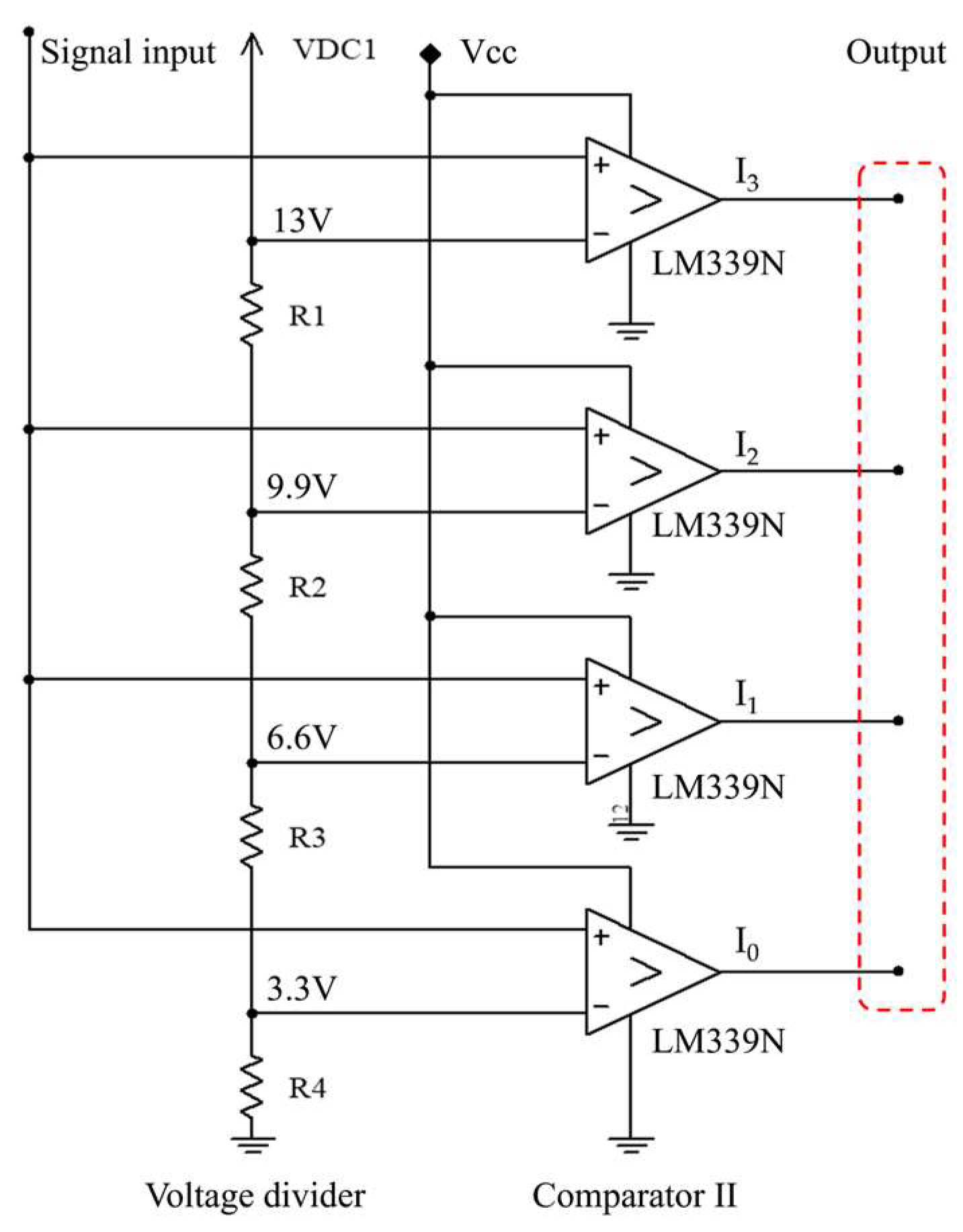
Figure 5.
Input/output ports of a 4:2 priority encoder.
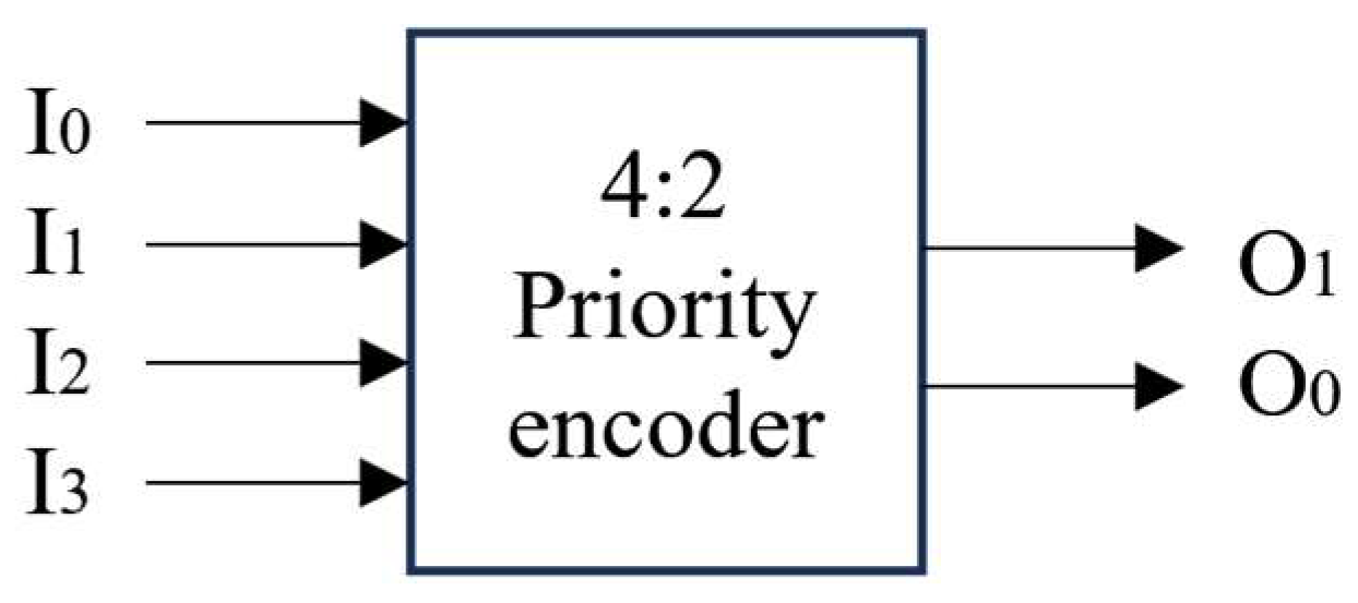
Figure 6.
Differential amplifier for providing the segmented waveform.
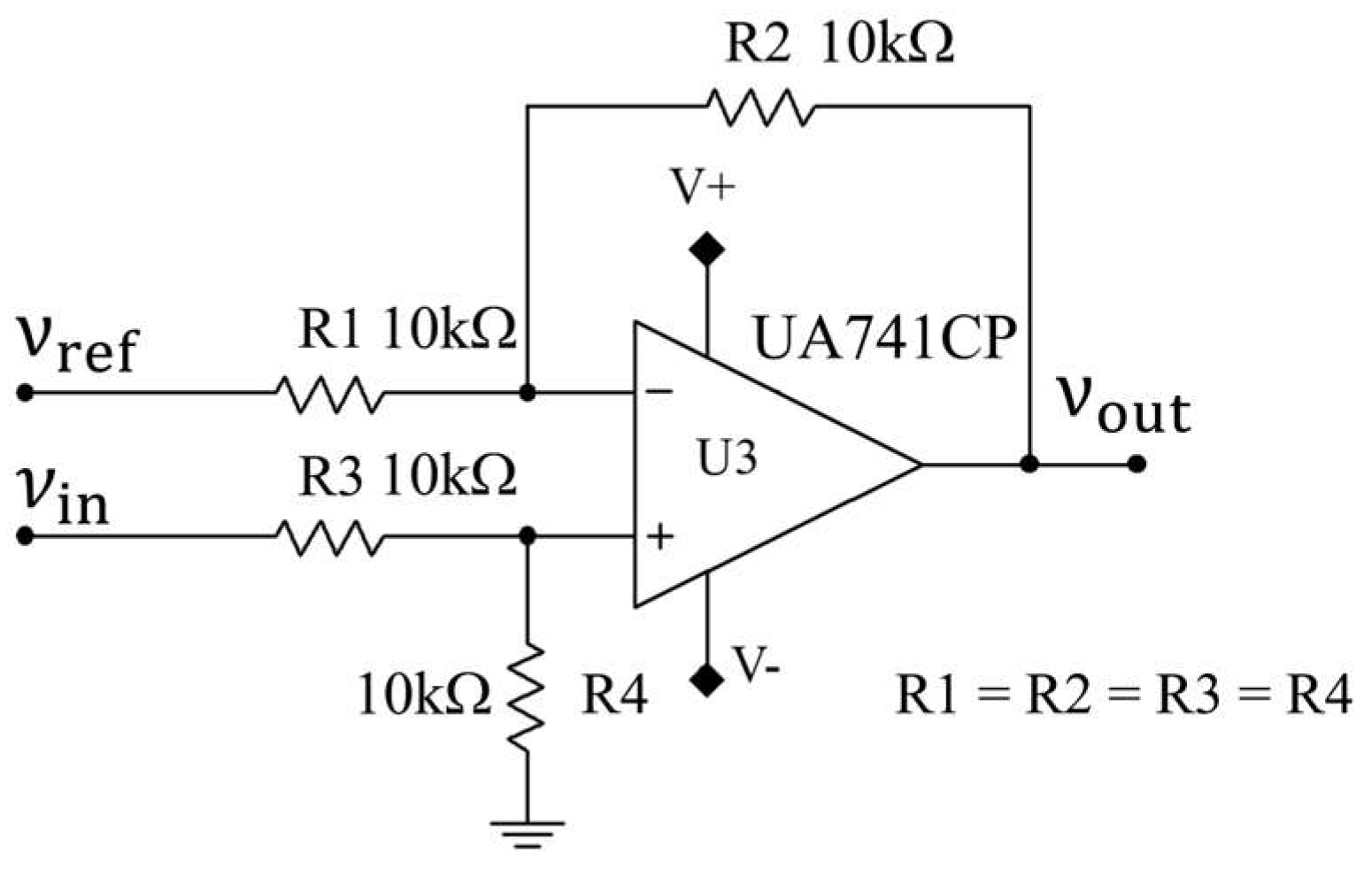
Figure 7.
Flowchart of waveform reconstruction program.
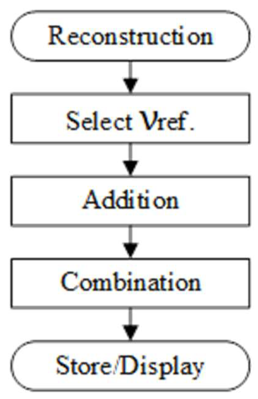
Figure 8.
Flowchart of selecting the reference voltage.

Figure 9.
Screen copies of program executions.
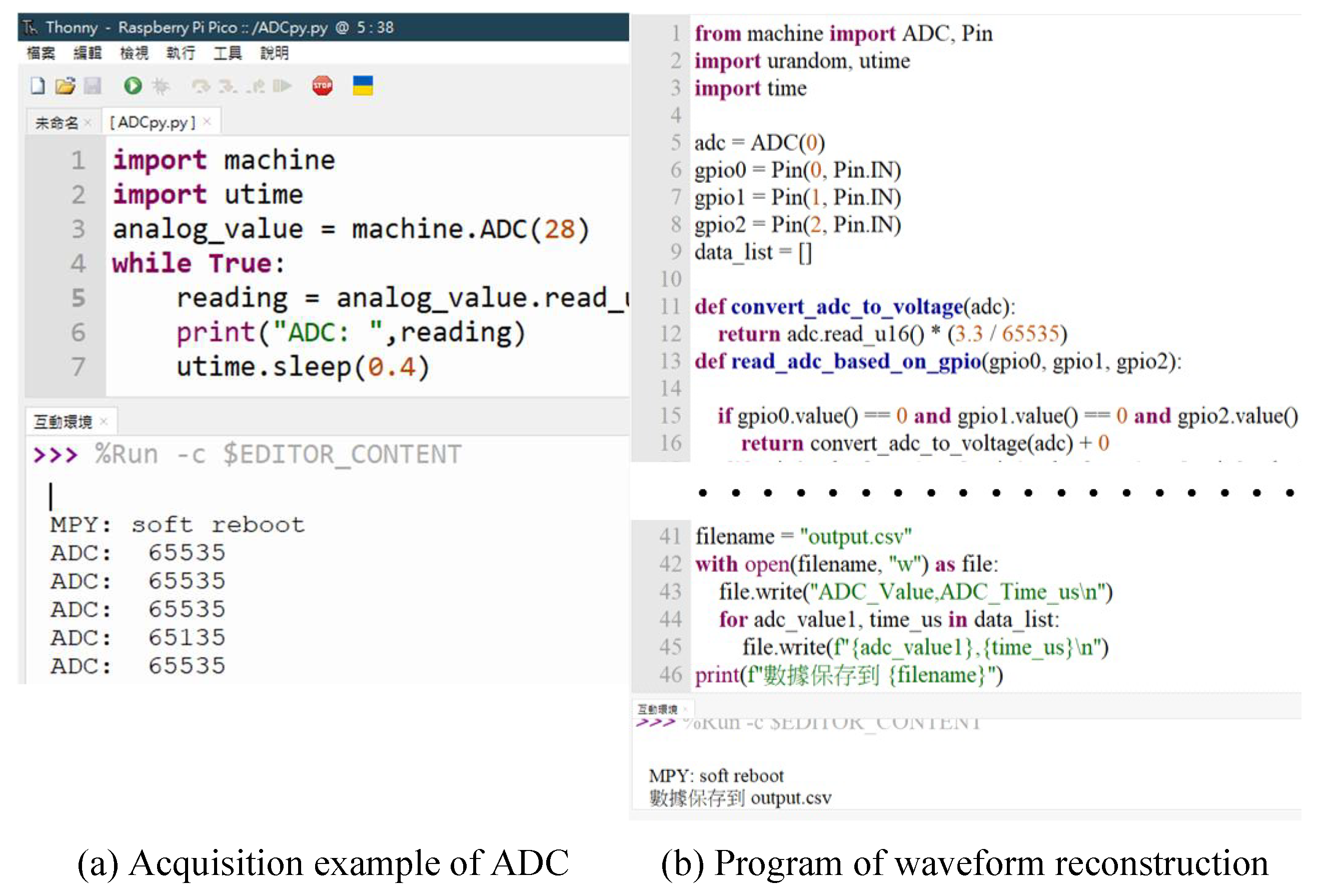
Figure 10.
Simulation results of reconstructed waveform and signals.
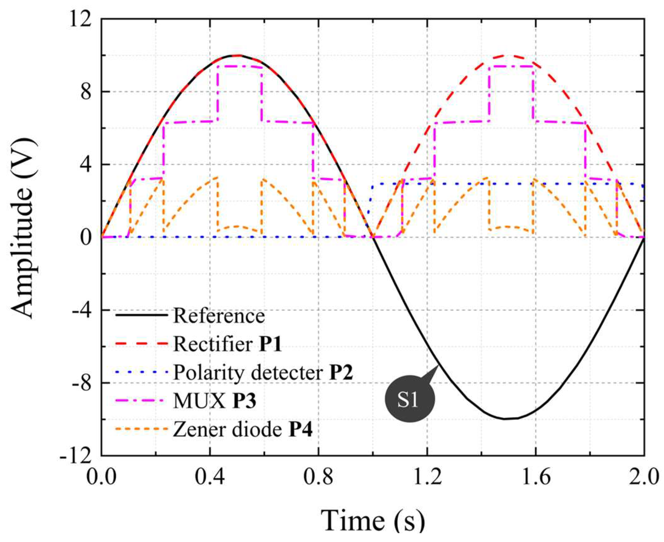
Figure 11.
Simulation results of reconstructed waveforms and errors.
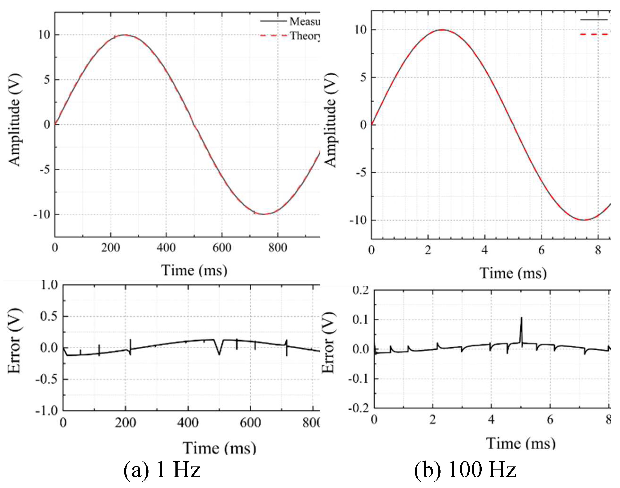
Figure 12.
Simulation results of the PV error affected by the frequency of waveform.
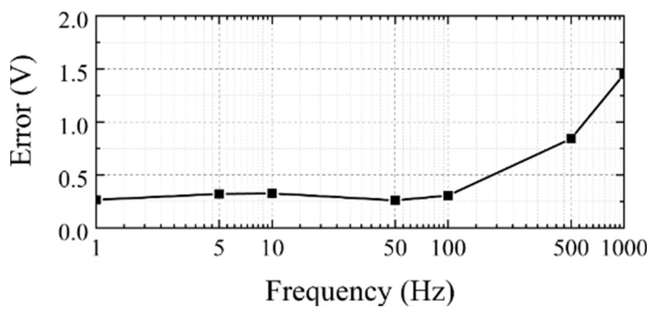
Figure 13.
Experimental setup for examining the performances of proposed SAS.
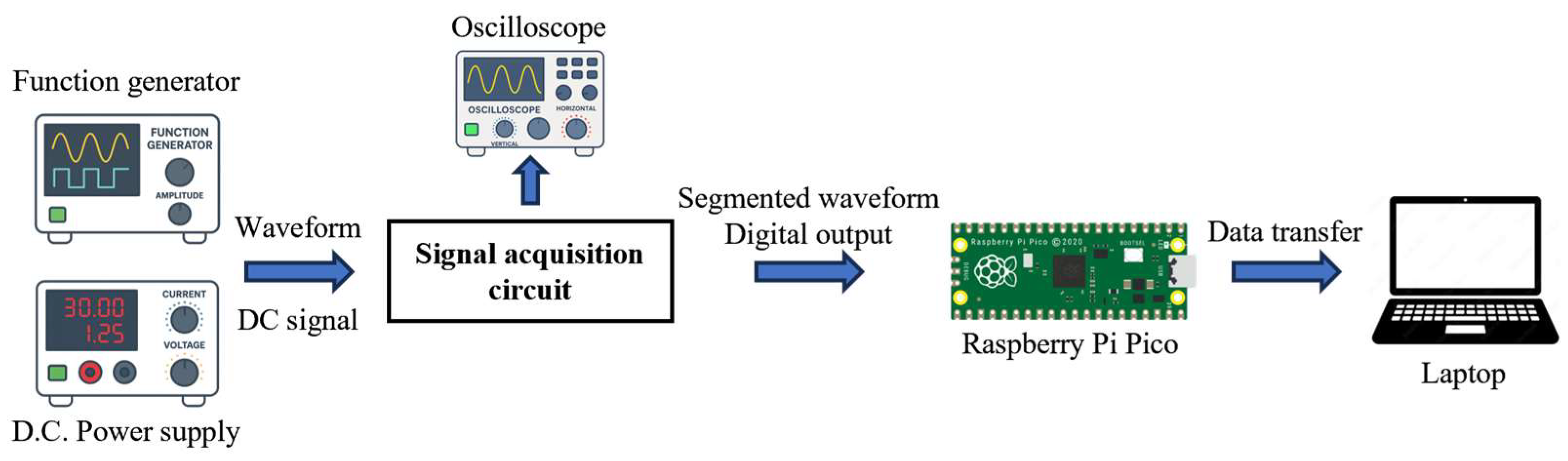
Figure 14.
Photograph of experimental setup.
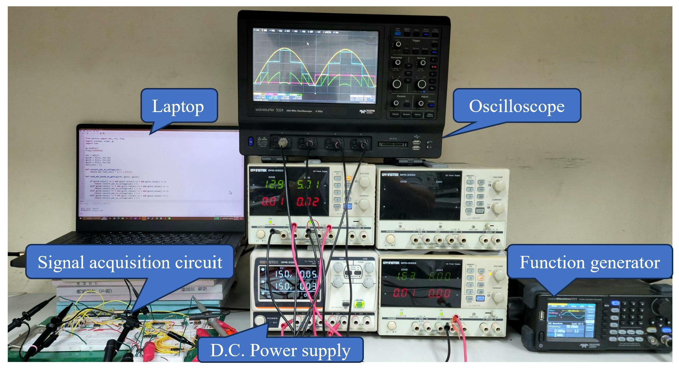
Figure 15.
Measured time delay of DC voltage.
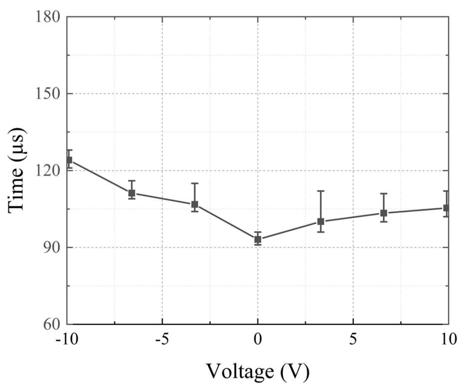
Figure 16.
Reconstructed waveform and measured signals based on SAS.
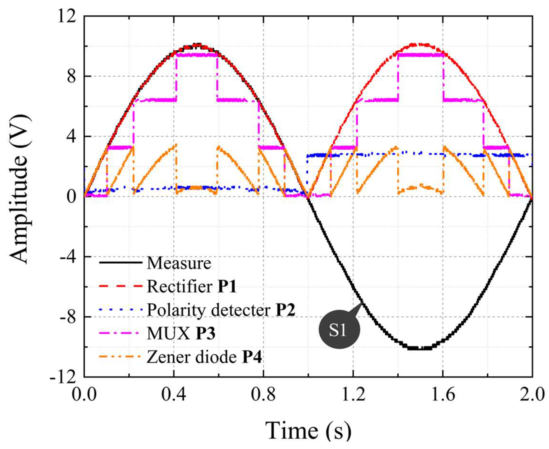
Figure 17.
Experimental results of reconstructed waveforms and errors.

Figure 18.
The measured PV error affected by frequency of waveform.
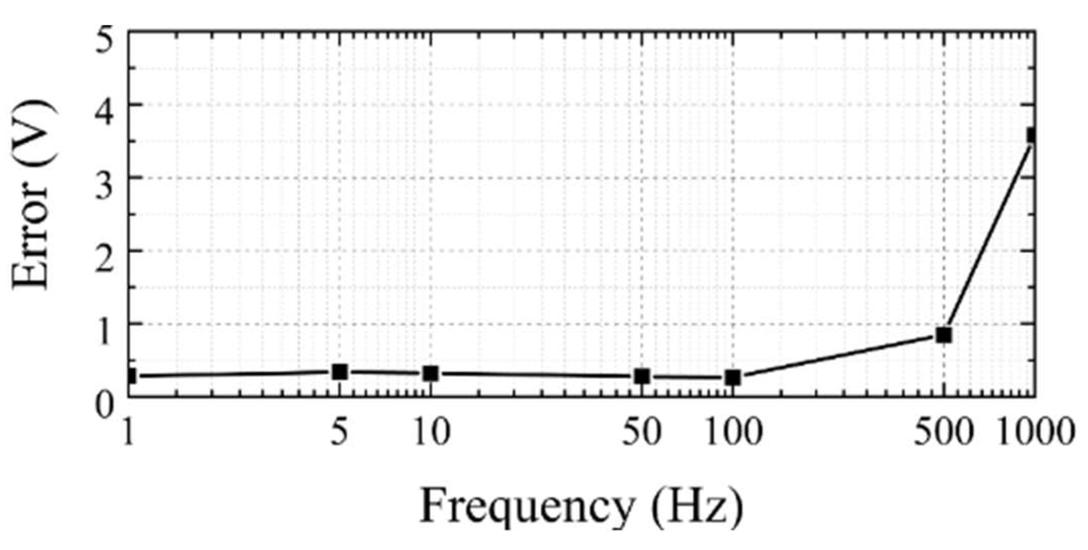
Figure 19.
The experimental setup for examining the attenuated waveform based on voltage divider.
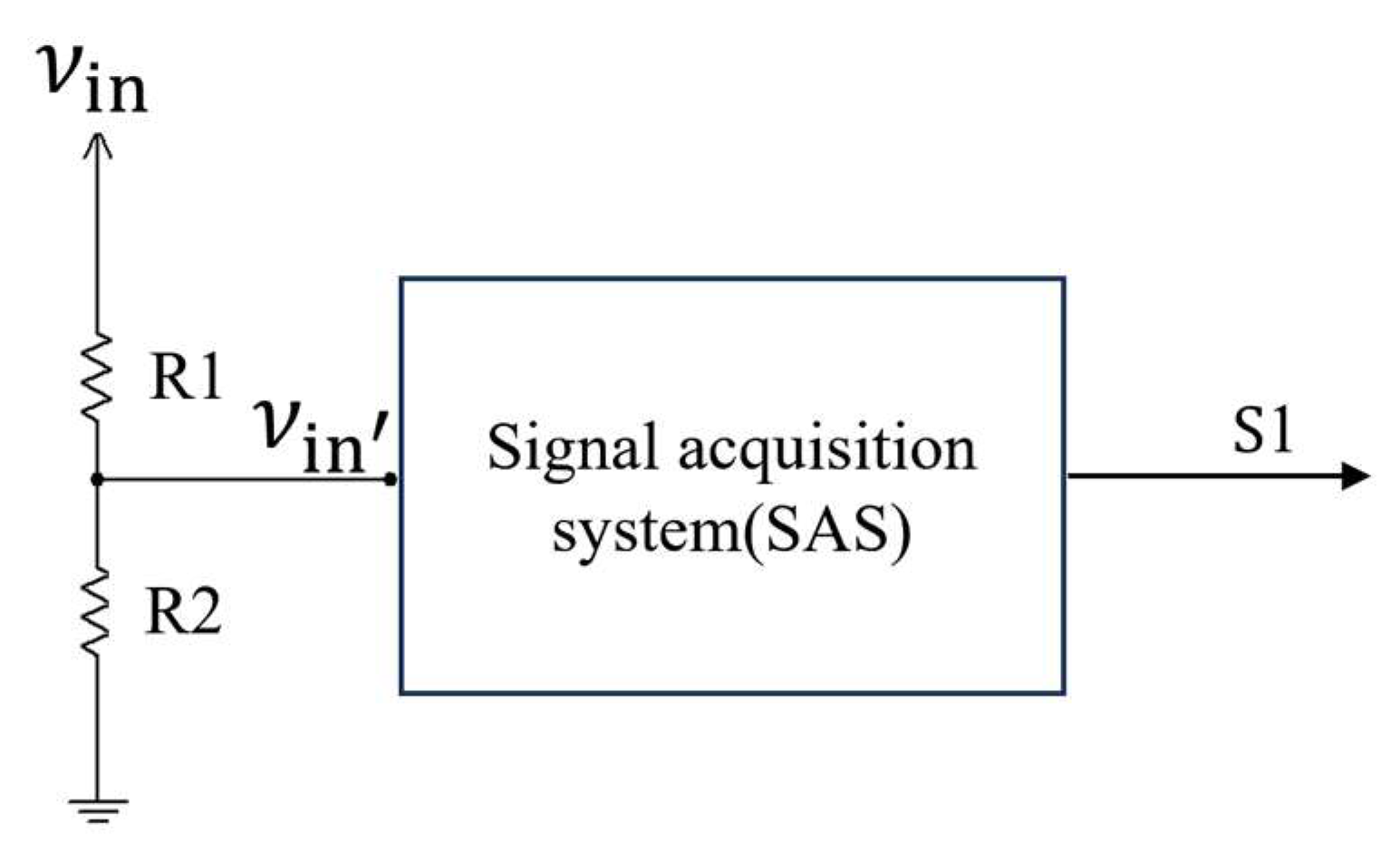
Figure 20.
Reconstructed waveforms and errors of the attenuated waveform.
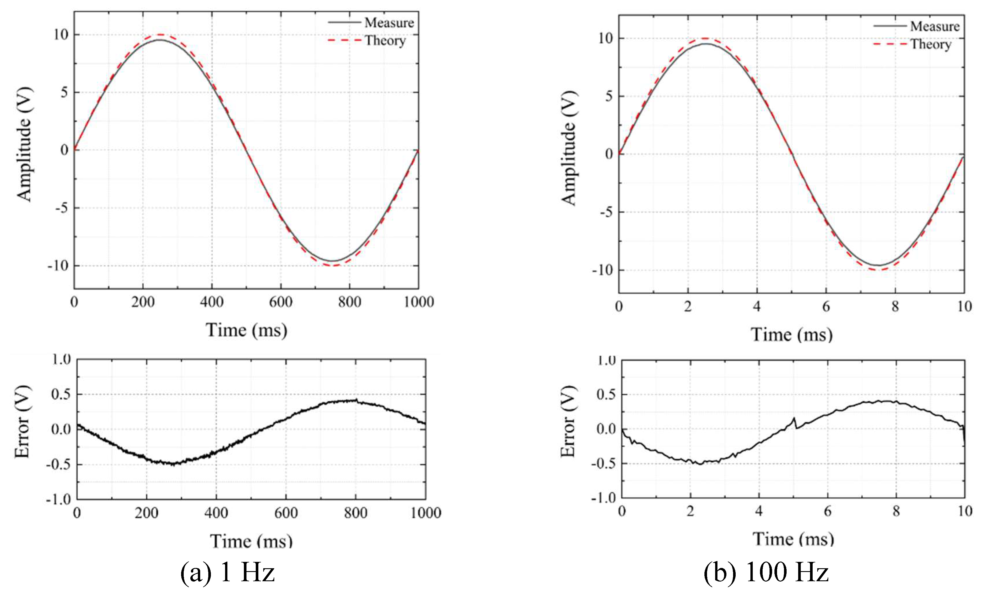
Figure 21.
The PV error affected by frequency of attenuated waveform.
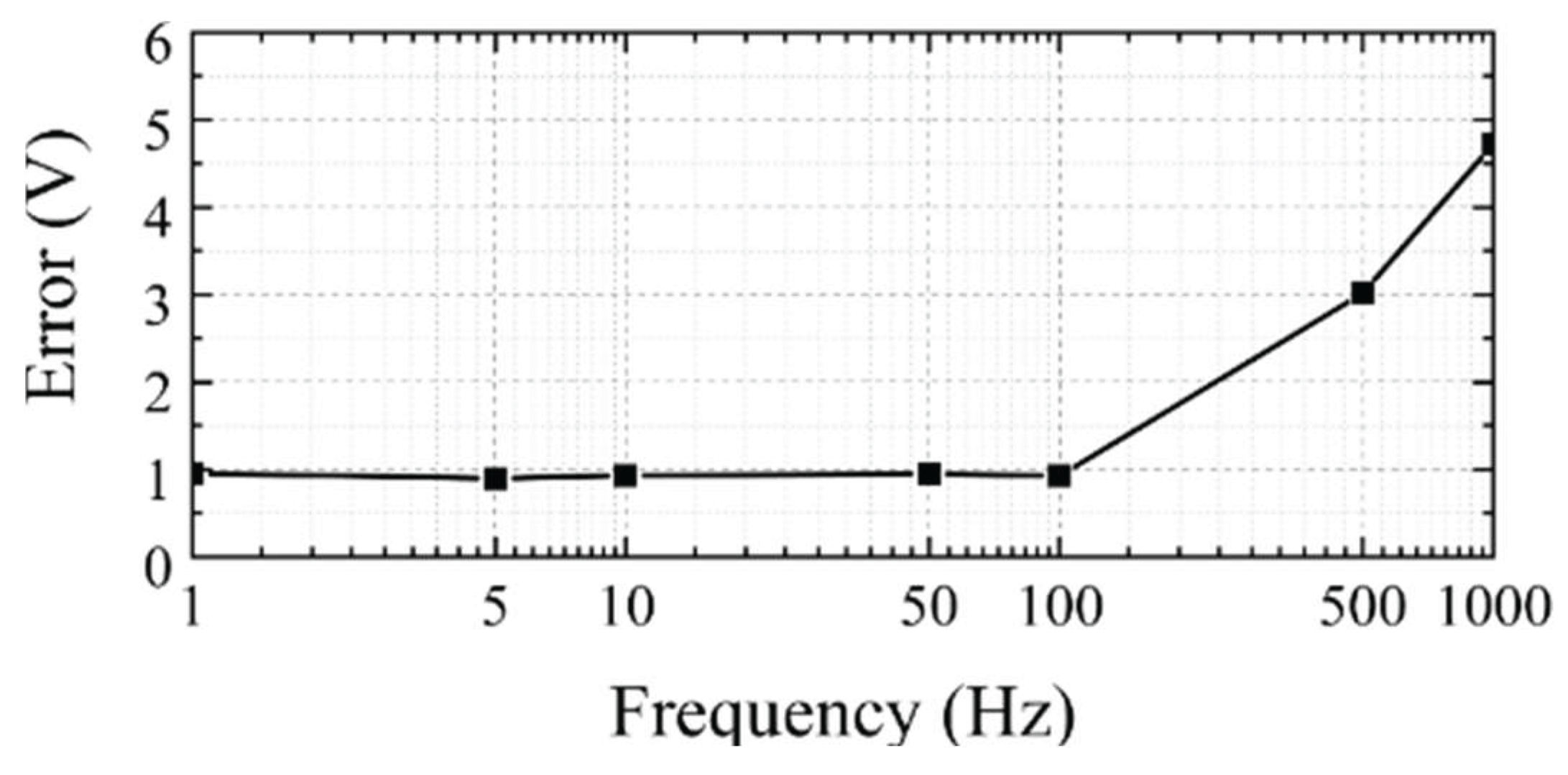
Table 2.
Main specifications of Pico.
| Microcontroller | Clock speed(MHz) | SRAM (Kbyte) | Flash memory (Byte) | ADC(bit) | ADC voltage range (V) | |
|---|---|---|---|---|---|---|
| Pico | RP2040 | 133 | 264 | 2M | 12 | 0~3.3 |
Disclaimer/Publisher’s Note: The statements, opinions and data contained in all publications are solely those of the individual author(s) and contributor(s) and not of MDPI and/or the editor(s). MDPI and/or the editor(s) disclaim responsibility for any injury to people or property resulting from any ideas, methods, instructions or products referred to in the content. |
© 2025 by the authors. Licensee MDPI, Basel, Switzerland. This article is an open access article distributed under the terms and conditions of the Creative Commons Attribution (CC BY) license (http://creativecommons.org/licenses/by/4.0/).
Copyright: This open access article is published under a Creative Commons CC BY 4.0 license, which permit the free download, distribution, and reuse, provided that the author and preprint are cited in any reuse.


