Submitted:
27 April 2025
Posted:
28 April 2025
You are already at the latest version
Abstract
Since its discovery, Laser Induced Graphene (LIG) attracted much interest because this technique, having all the advantages of a laser processing technology, is more convenient and cost-effective than other graphene production methods. This work offers a detailed analysis of LIG structures produced by UV and CO2 laser irradiation from polyimide performed with surface scanning Raman spectroscopy combined with microscopy techniques. Although UV LIG has a less ordered structure than that obtained by CO2 laser irradiation, our study indicates that UV LIG can be patterned with a resolution higher than that obtained with CO2 laser irradiation and much smaller penetration depth into the substrate.
Keywords:
Laser-induced graphene
; Fabrication process
; Raman spectral imaging
; Confocal Laser microscopy
1. Introduction
Laser-Induced Graphene (LIG) is porous graphene obtained by laser scribing a suitable polymer as polyimide (PI). The laser induced reactions transform PI surface into interconnected sheets with honeycomb structure. Since its discovery, LIG attracted much interest because this technique has the advantages of all laser processing technology as controllable, non-contact, space-resolved and non-catalytic operation mode [1,2]. Moreover, the LIG can be obtained at room temperature without any polymer pre-treatment, which makes this process more convenient and cost-effective than other graphene production methods. LIG has a wide range of applications due to its unique properties, including high electrical conductivity, large surface area, and biocompatibility.
In 2014 the first LIG was obtained from commercial PI using CO2 infrared lasers, circumventing the necessity of high temperatures and vacuum chambers of Chemical Vapor Deposition (CVD) graphene fabrication. Hereafter, several studies have been performed exploring this process with different lasers [3]. Lasers emitting UV wavelengths can induce mainly photolysis reactions whereas IR lasers produce pyrolysis processes.
LIG has a three-dimensional structure with pronounced distortion of six-membered rings. Moreover, differently to honeycomb lattice observed in two-dimensional (2D) graphene, in LIG there is a significant abundance of five-, seven-, membered rings [4,5].
The easy production combined with the unique porous structure make LIG graphene a valuable material for future technologies as supercapacitors and batteries with high energy density and fast charging rates, flexible and printable electronic devices, such as sensors for activity monitoring, water filtration and other environmental remediation applications, etc [1]. This form of graphene is also resistant to biofilm formation [5,6].
In this work, we used UV and CO2 laser scribing to grow LIG from PI. LIG samples were characterized by Raman confocal spectroscopy with surface scanning, Confocal Laser Scanning Microscopy (CLSM), Scanning Electron Microscopy (SEM), Atomic Force Microscopy (AFM) and Water Contact Angle (WCA), with the aim to explore the differences between UV and CO2 LIG structures. As precursor, we used PI in the form of Kapton film. Looking at literature data, we found that, although it is possible to obtain LIG from various polymers and organic substrates, PI is the most common used precursor [3,7]. Kapton has a significant optical transmittance in the 10.6 µm region and absorbs UV light, therefore for irradiation with CO2 laser it is better to use thicker Kapton substrate because due to the photothermal process a buckling of substrate is observed [5,8,9]. To this respect, the substrate deformation, leading to non-flat device, limits the application of LIG [10], while the use of UV light, due the ability to have a more focused spot, allows for both thinner and narrower devices. After all, Kapton has a widespread application in aerospace, it is used in spacecraft, satellites, and various space instruments due to its thermal stability, radiation resistance, and low outgassing and consumer electronics, it is used in flexible printed circuits, insulation for wires and cables, and as a substrate for solar cells.
Our measurements indicate that UV LIG has a less ordered structure than CO2 LIG with a smaller pore size in the flakes, although it can be obtained in the form of laser patterned structure.
2. Materials and Methods
2.1. LIG Sample Preparation
As LIG precursor we used a PI film in the form of Kapton adhesive tape (Dupont, 16 mm width, about 65 µm thickness) on glass substrate (see Figure 1). The as prepared samples were irradiated with UV nanosecond INNOLAS laser (maximum power = 5 W, F-theta lens = 100 mm, laser spot ≈ 10 µm) and CO2 laser (maximum power = 80 W, F-theta lens = 100 mm, laser spot ≈ 100 µm). Different lines were scribed varying laser power and scanning speed. LIG surfaces were obtained scribing adjoined lines, as shown in Figure 1.b. The LIG square dimensions of Figure 1b. are about (5 × 5) mm2.
2.1. LIG Characterizations
2.1.1. Surface Scanning Confocal Raman Spectroscopy
Raman spectroscopy is a nondestructive well-established technique for investigating graphene properties. Raman spectra were acquired with a Horiba XploRA Plus micro-Raman confocal spectrometer operating in the range 100-3500 cm-1 with a laser excitation of 532 nm. We used a laser power of 1,5 mW to avoid heat influenced alteration of Raman spectra and damaging of the samples. To obtain the detailed structural properties, the samples were scanned point by point of a prefixed grid selecting areas down to (5 × 5) μm2 using an objective with 100x magnification that gives a laser spot size of about 800 nm and up to (300 × 350) μm2 using an objective of with 10x magnification which gives a laser spot size of about 1.7 µm and selecting the “Mosaic” option in the microscope scanning mode.
The typical vibration features of graphene are the tangential mode G (1580 cm–1) assigned to the stretching of sp2 atom pairs, and the D band at 1350 cm–1 with its second order (labeled as 2D in Figure 2). While G and 2D bands always satisfy the momentum conservation requirement in the Raman scattering process, the D peak can be observed only in the presence of defects, which provide the missing momentum necessary to fulfill the momentum conservation rule [11,12,13,14]. Therefore, its intensity is proportional to the number of defects in the graphene lattice and, as discussed in the following, the intensity ratio of D versus G band (ID/IG) is commonly used for quantifying disorder.
For a given sample the sp2 crystalline structure is preserved for a length L, which can be considered either as the dimension of in-plane crystallite or as the distance between two neighboring defects [11,12,15,16]. This length can be calculated through the ID/IG ratio that is inversely related to the crystallite size L, and proportional to the defect density ND according to the Tuinstra and Koenig relations:
where λL and ΕL are the laser excitation wavelength (532 nm) and the energy (2.3 eV) used for exciting the Raman spectra [11,17,18].
The intensity and shape of 2D band is sensitive to the z - stacking order of graphene layers, therefore the I2D/IG ratio is widely used to distinguish among single-layer or bilayer and multilayer graphene. In the mono-layer graphene, the 2D band is observed as symmetric peak, that can be fitted as single Lorentzian with a width = 30 cm–1 and the I2D/IG intensity ratio is larger than 2.0., as reported for non-doped CVD grown single-layer graphene [11,12,13,14]. The defect density also affects the intensity of 2D band, because defects reduce the electronic lifetime leading to smaller intensity and larger line width of Raman peaks [19,20].
The Raman spectra of irradiated samples were fitted through Classical Least Square (CLS) fitting method, to calculate the specific contribution of different components, graphene and PI, in given spectrum. As components (loadings) traces, we used the Raman spectra of mono-layer CVD grown graphene [15] and that of Kapton before irradiation.
The measured Raman spectra have been expressed as linear combination of loadings reported in Figure 2 with suitable coefficients, named scores. The normalized score of graphene loading was used to follow the onset of Kapton carbonization as function of laser writing process.
2.1.2. Confocal Laser Scanning Microscopy
LIG samples were analyzed by a CLSM Nikon 80i-C1 operating in laser reflection mode. The samples were illuminated by a 532 nm continuous laser (with a nominal output power of 3 mW). The reflected signal collected by a 20x objective (scanning the sample in a xy field of view of (633x633) µm2) was detected by a photomultiplier point by point. The CLSM is a significant evolution of the conventional optical microscope. By scanning along the z optical axis, the CLSM performs an optical sectioning of the observed sample by using a pinhole in front of the detector positioned in a conjugate plane with respect to the focus one and detecting only signals from the in-focus plane by eliminating signals from out-of-focus ones. The optical sectioning allows obtaining a tridimensional (3D) reconstruction of the sample [21]. By using the optical sectioning operation of the CLSM system, several 2D (xy) slices along the optical z axis with controlled spatial increments (z scanning step = 3 µm) were detected. After acquisition of the 2D slices with a z scanning intervals of (0-50) µm and (0-70) µm (depending on the thickness of the samples), 3D reconstructions of the images have been performed by the software of the confocal microscope.
2.1.3. Water Contact Angle
The wetting properties of the samples have been investigated through a custom-built optical setup for contact angle measurements. The setup includes a fiber illuminator that backlights the sample, which is placed on an adjustable sample holder. A portable Dino-Lite AM4515ZT digital microscope is connected to a computer running the acquisition software (DinoCapture 2.0). This configuration enables the visualization and the acquisition of magnified droplet images, facilitating contact angle analysis.
2.1.4. Atomic Force Microscope
Topographic surface analyses were performed with Park System XE-Atomic Force Microscope (AFM) operating in non-contact mode. Pre-mounted non-contact, high-resolution cantilevers working at 309 MHz with nominal tip radius below 10 nm were used. Images were flattened by subtracting a linear background for the fast scan direction and a quadratic background for the slow scan direction.
2.1.5. Scanning Electron Microscope
For SEM characterization we used an Electron Microscope Tescan Vega, with thermionic source and tungsten filament. The resolution was 3 nm with an accelerating voltage of 30kV.
3. Results
3.1. UV Laser Irradiation
To investigate the effect of laser power, LIG lines were scribed keeping constant at 5 mm/s the scanning speed and increasing the UV laser power. The laser power increases from line 1 to line 8. The optical images of selected lines 1, 5, 6, 8 and the corresponding Raman spectra acquired for each line are reported in Figure 3.a and 3.b, respectively.
The Raman spectral features of Kapton PI at 1120 cm-1 (C-N-C stretching), 1420 cm-1 (C-N stretching) and 1740 cm-1 (C=O stretching) progressively disappear from line 1 to line 8 giving rise to D, G and 2D band of graphene. These changes indicate that laser irradiation initiates the PI graphitization increasing the C–C bonds and decreasing the C–O and C-N bonds. This is proportional to the laser power.
Following the procedure described in the previous paragraph, the graphene scores were calculated and reported in Figure 3.c for each line. From line 5 to line 6 the graphene score increases from 45% to 65 %, pointing to a threshold-power that was observed also in UV ablation of polymers [10]. By increasing the laser power, the line width increases, whereas, as observed by other authors, by increasing the scan rate higher threshold power is needed to initiate the graphitization. Increased laser power leads to higher values of graphene score, up to 90%, proving that laser irradiation of PI material can form the graphene structure breaking nitrogen and oxygen bonds, releasing them as gases.
As already discussed, Raman spectroscopy is a powerful tool to obtain the crystal size (L) by analyzing ratios of the intensities of D and G peaks. For line 8 the ID/IG ratio is 0.84, the L value calculated using equation (1) is 25 nm, to be compared with the value of 40 nm obtained by other authors [5]. The I2D/IG value is 0.30, indicating that in line 8 multi-layer graphene is formed with a defect density, from equation (2), of 1.72 ∙1011 cm-2. The defects are mainly due to the high density of edges, derived from the foamy nature of the material. It is worth noticing that there is large shoulder due to a residual C-N bonds content between the D and G band. The Raman spectra point to the formation of graphene although we are far from the Raman trace of CVD grown graphene shown in Figure 2.
LIG patterned squares with dimensions up to of 1 cm2 were scribed with different irradiation conditions by using a step size of 10 µm, to obtain adjoined lines. The optical images of UV LIG squares are shown in Figure 4.a, for scribing the Q1_UV and Q2_UV squares we used the parameters of lines 7 and 8 respectively, for Q4_UV_KN we used the same conditions of Q2_UV with a faster scanning speed.
The Raman spectra in the upper panel of Figure 4.b evidence the formation of graphene with a ID/IG ranging from about 0.3 to 0.45 for Q2_UV; in this case an almost total conversion of the Kapton is achieved being the graphene score 91%. The Raman maps in Figure 4.c are plotted by using as contrast parameter the intensity of G peak normalized to the area of whole spectrum. In the used color code, the intensity increases from brown to red, yellow colors. The yellow stripes correspond to the center of laser scans.
Figure 5.a reports the 3D CLSM image of LIG square Q2_UV. The LIG structure presents a periodic pattern with a period of about 10 µm as shown in the graph of Figure 4.b, reporting the intensity profile along the yellow arrow of Figure 5.a, in correlation with the spot size of the UV writing beam. Figure 5.c reports a selected xz 3D projection of Figure 5.a and the measured surface z modulation is less than 10 µm, therefore the LIG writing process with focused UV laser beam with a theoretical spot size of about 10 µm is a technique that could be applied to even thinnest substrates.
Due to the faster scanning speed, the stripes in the sample Q4_UV_KN have a smaller width (see Figure 6) with a smaller surface corrugation.
The Raman map of the normalized G peak intensity of LIG square Q2_UV reported in Figure 7a clearly shows that the UV laser has written graphene with a patterning comparable to that observed by CLSM reported in Figure 7.b. The graphene formation occurs across all the irradiated substrate, as evidenced in Figure 7.c and 7.d. with only a slight difference in the I2D/IG ratio.
3.2. CO2 Laser Irradiation
Figure 9.a presents the Raman spectra of the CO2 laser irradiated Kapton surface, imaged in Figure 9.b, using different laser powers. By increasing the laser power, the ID/IG decreases from 1.0 to 0.5 improving the crystalline nature of the ablated surface, the shoulder due to the residual C-N bonds decreases and the increase of the I2D/IG ratio from 0.3 to 0.8 points to a reduction of the number of graphene layers. The crystal size evaluated from (1) is 42 nm, larger than obtained with UV irradiation.
The Raman maps of normalized G peak intensities, reported in Figure 9.c, evidence that the graphene formation is localized only on the laser scribed regions. In the Q3 and Q4 samples the scribing laser spot size is 100 µm and the used scanning step is 100 µm. In the sample Q3 the highest intensity G peak yellow region is in the center of the spot, while by increasing the laser power, the G peak intensity is uniform on the spot. For the other two samples the laser was focused down to 50 µm, obtaining a large G peak intensity across the whole surface, in the sample Q2_KN the adjacent lines were scribed with a step size of 30 µm and we obtained a patterning of large G peak intensity yellow region alternated with a smaller G peak intensity orange region. The graphene score calculated with the CLS fitting resulted to be 85% for the Q3_CO2 sample and about 93% for the others.
Figure 10.a reports the 3D CLSM images of Q3_CO2 and Q4_CO2 samples. The treated LIG surface appears higher (in the Z scanning) than the not irradiated Kapton surface showing a rise effect due to photothermal process. In the yellow rectangles of Figure 10.a, xz and yz slices selected along the dotted yellow lines are reported showing the z distribution (in a z interval of (0-70) µm) of the sample along its thickness. The CO2 laser scanning with a 100 µm patterning period is clearly visible in the xy intensity profiles of Figure 10.b for Q3_CO2 and Q4_CO2 LIG patterned squares.
The selected 3D projections are reported in Figure 10.c highlighting the rising effect in the z direction, whose amount of about 43 µm has been measured in Q3_CO2 sample, with a slight increase for the Q4_CO2 sample scribed at larger power.
We performed the same characterization for the other two LIG samples obtained by CO2 laser writing and we measured a similar rising effect in the z direction up to 54 µm, as shown in Figure 11. The intensity profile shows a continuous roughened surface for the Q1_CO2_KN sample, whereas that of Q2_CO2_sample is patterned following the laser scanning step. This patterned structure with ordered variation in z direction could be suitable for growing biological samples.
3.3. Morphological Comparison Between UV and CO2 Laser LIG Structures
The SEM analysis reported in Figure 12 shows the microstructures of the patterned lines in the UV and CO2 LIG squares.
In Figure 12.a the low-resolution image of Q2_UV LIG square clearly shows that the stripes of the pattern have a width of 10 µm. The images at higher magnification of Figure 12.a report a structure quite different from the foamy structure of CO2 laser LIG of Figure 12.b: the UV LIG stripes seems to be composed by flat flakes staggered onto each other with pores of few µm. Differently, it can be observed that porous carbon dominates the middle of each pattern of 50 µm width Q1_CO2_KN stripes. The pores have a larger size that ranges from 5 to 10 µm.
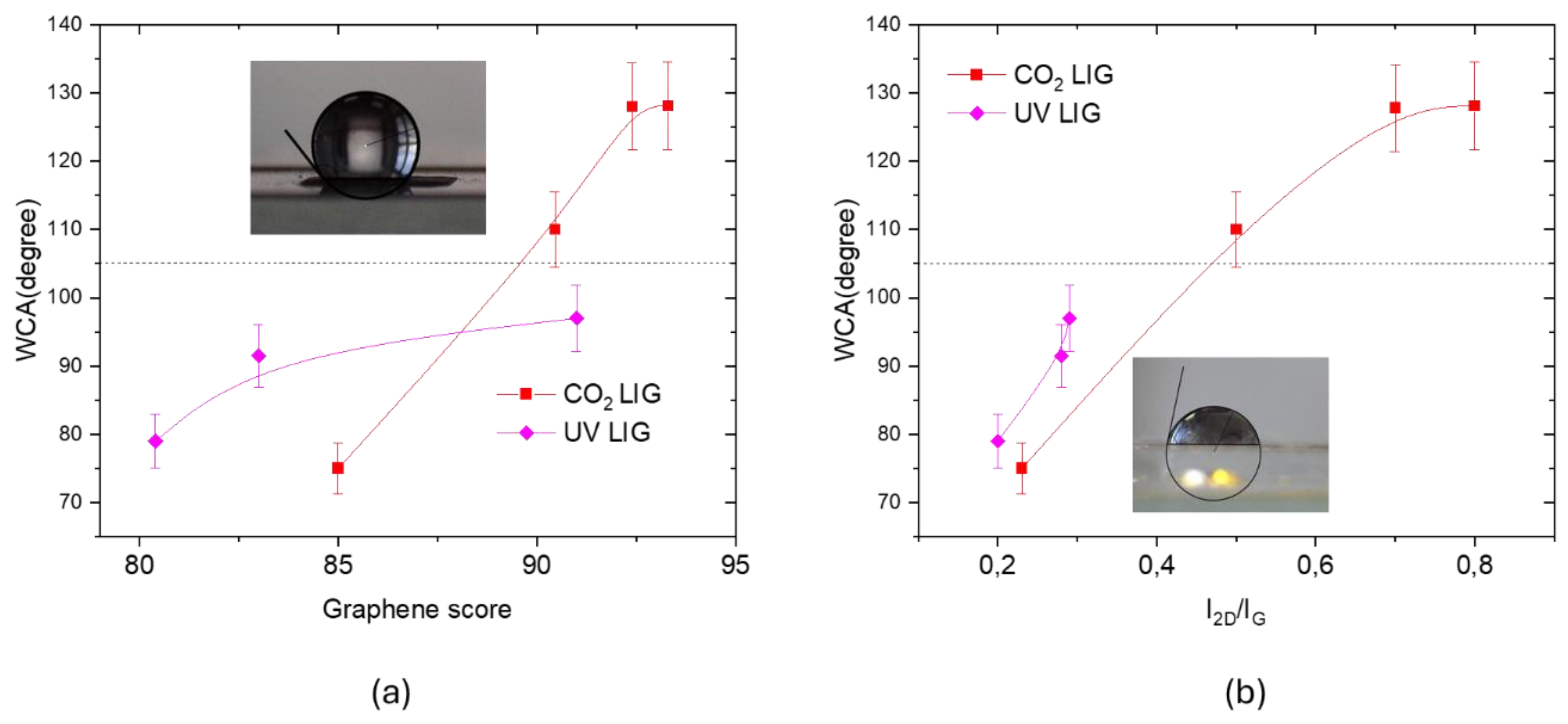
Such differences in the structures of UV and CO2 LIG can explain the variability of measured WCA, shown in Figure 13. As expected, the WCA value increases with the graphene score calculated with CLS fitting and with the I2D/IG ratio, namely with the graphene content and with its quality. In fact, graphene has a hydrophobic behavior, with a WCA= (105 ± 5) ° [22], that is a complex issue with several contributing factors. The carbon-carbon bonds in the hexagonal lattice are nonpolar covalent bonds, the lack of polarity means there are no strong electrostatic interactions with polar water molecules. Moreover, pristine graphene has a relatively low Surface Energy (around 46-62 mJ/m²) [23]. Water, with a high surface tension (around 72 mJ/m² at room temperature), tends to minimize its contact area with low-energy surfaces to reduce its own energy, leading to high contact angle.
The WCA values of about 128 ° measured for the CO2 LIG are larger than those measured for UV LIG, this finding can be explained considering that CO2 laser irradiation process creates a porous, three-dimensional network that significantly increases the surface roughness. A rough surface can trap air pockets, minimizing the contact area between water droplets and the solid surface, leading to a high-water contact angle and in some cases to superhydrophobic behavior.
4. Discussion
The measured Raman spectra should point to the production of lower-quality graphene with UV laser irradiation, with a larger content of defects and number of layers. SEM and AFM inspections point to a different structure: the CO2 laser facilitated the formation of micrometer-sized pores and spongy structure, while UV LIG exhibits flakes with limited pore occurrence. The three-dimensional profiles measured by CLSM indicate that a raised structure was formed on PI by using CO2 laser whereas a quasi-planar concave structure is formed on PI by using a UV laser. Such differences can be mainly ascribed to the fact that CO2 laser irradiation is a photothermal process with high temperatures that are maintained for longer tomes, whereas the UV irradiation with shorter wavelength, enables the photons to possess energy greater than the dissociation energy required for breaking chemical bonds within the material. Notably, the UV LIG has a surface size considerably smaller than that achieved with infrared laser. In our experiment we obtained a patterned LIG with 10 µm width.
5. Conclusions
The obtained results validate the possibility of UV laser to induce graphene on the PI surface. Overall, our study demonstrates that UV LIG has a less ordered structure that that obtained by CO2 laser irradiation. Besides that, UV LIG can be patterned with a resolution higher than that obtained with CO2 laser irradiation and much smaller penetration depth into the substrate, opening the way for the application of this technology for flexible electronics field that requires planar device.
Author Contributions
Conceptualization, S.B. and F.B.; methodology S.B., F.B., A.B.; validation, S.B. and F.B.; formal analysis, S.B. and F.B.; investigation, S.B., F.B., A.B., F.M., V.N., A.R., A.V.; data curation, S.B. and F.B.; writing—original draft preparation, S.B.; writing—review and editing, S.B., F.B., A.B., F.M., V.N., A.R., A.V.
Funding
This research received no external funding.
Institutional Review Board Statement
n. a.
Informed Consent Statement
n. a.
Data Availability Statement
The data of this research are available upon reasonable request.
Conflicts of Interest
A. B. is employee of Optoprim s.r.l whose laser scribing systems were used in the present work. There are no other conflicts of interest.
References
- Zhang, Z.; Zhu, H.; Zhang, W.; Zhang, Z.; Lu, J.; Xu, K.; Liu, Y.; Saetang, V. A review of laser-induced graphene: From experimental and theoretical fabrication processes to emerging applications. Carbon 2014, 118356. [Google Scholar] [CrossRef]
- Lin, J.; Peng, Z.; Liu, Y.; et al. Laser-induced porous graphene films from commercial polymers. Nat. Commun. 2014, 5, 1–8. [Google Scholar] [CrossRef]
- Loh, K.P.; Bao, Q.; Ang, P.K.; et al. The chemistry of graphene. J. Mater. Chem. 2010, 20, 2277–2289. [Google Scholar] [CrossRef]
- Ye, R.; James, D.K.; Tour, J.M. Laser-induced graphene: from discovery to translation. Adv. Mater. 2019, 31, 1803621. [Google Scholar] [CrossRef] [PubMed]
- Chen, Y.; Long, J.; Zhou, S.; Shi, D.; Huang, Y.; Chen, X.; Gao, J.; Zhao, N.; Wong, C.P. UV Laser-Induced Polyimide-to-Graphene Conversion: Modeling, Fabrication, and Application. Small Methods 2019, 3, 190020. [Google Scholar] [CrossRef]
- Ma, W.; Zhu, J.; Wang, Z.; et al. Recent advances in preparation and application of laser-induced graphene in energy storage devices. Mater. Today Energy 2020, 18, 100569. [Google Scholar] [CrossRef]
- Lin, J.; Peng, Z.; Liu, Y.; et al. Laser-induced porous graphene films from commercial polymers. Nat. Commun. 2014, 5, 55714. [Google Scholar] [CrossRef]
- Choi, W.; Lahiri, I.; Seelaboyina, R.; et al. Synthesis of graphene and its applications: a Review. Crit Rev Solid State 2010, 35, 52–71. [Google Scholar] [CrossRef]
- Ismail, A.M.; Nasrallah, D.A.; El-Metwally., E.G. Modulation of the optoelectronic properties of polyimide (Kapton-H) films by gamma irradiation for laser attenuation and flexible space structures. Radiation Physics and Chemistry 2022, 194, 110026. [Google Scholar] [CrossRef]
- Carvalho, A.F.; Fernandes, A. J.S.; Leitão, C.; Deuermeier, J.; Marques, A.C.; Martins, R.; Fortunato, E.; Costa, F. M. Laser-Induced Graphene Strain Sensors Produced by Ultraviolet Irradiation of Polyimide. Adv. Funct. Mater. 2018, 28, 1805271 (1–8). [Google Scholar] [CrossRef]
- Ferrari, A. C.; Robertson, J. Interpretation of Raman spectra of disordered and amorphous carbon. Phys. Rev. B: Condens. Matter Mater. Phys. 2000, 61, 14095–14107. [Google Scholar] [CrossRef]
- Ferrari, A. C. Raman spectroscopy of graphene and graphite: disorder, electron-phonon coupling, doping and non-adiabatic effects. Solid State Commun. 2007, 143, 47–57. [Google Scholar] [CrossRef]
- Ferrari, A. C.; Basko, D. M. Raman spectroscopy as a versatile tool for studying the properties of graphene. Nat. Nanotechnol. 2013, 8, 235–246. [Google Scholar] [CrossRef]
- Mallard, L. M.; Pimenta, M. A.; Dresselhaus, G.; Dresselhaus, M. S. Raman spectroscopy in graphene. Phys. Rep. 2009, 473, 51–87. [Google Scholar] [CrossRef]
- Botti, S.; Mezi, L.; Rufoloni, A.; Vannozzi, A.; Bollanti, S.; Flora, F. Extreme Ultraviolet Generation of Localized Defects in Single-Layer Graphene: Raman Mapping, Atomic Force Microscopy, and High-Resolution Scanning Electron Microscopy Analysis. ACS Appl. Electron. Mater. 2019, 12, 2560–2565, https://pubs.acs.org/doi/10.1021/acsaelm.9b00566. [Google Scholar] [CrossRef]
- Cancado, L. G.; Takai, K.; Enoki, T.; Endo, M.; Kim, Y. A.; Mizusaki, H.; Speziali, N. L.; Jorio, A.; Pimenta, M. A. Measuring the degree of stacking order in graphite by Raman spectroscopy. Carbon 2008, 46, 272–291. [Google Scholar] [CrossRef]
- Tuinstra, F.; Koenig, J. L. Raman spectra of graphite. J. Chem. Phys. 1970, 53, 1126–1310. [Google Scholar] [CrossRef]
- Lucchese, M.M.; Stavale, F.; Ferreira, E.H. M.; Vilani, C.; Moutinho, M.V.O.; Capaz, R. B.; Achete, C.A.; Jorio, A. Quantifying ion-induced defects and Raman relaxation length in graphene. Carbon 2010, 48, 1592–1597. [Google Scholar] [CrossRef]
- Casiraghi, C.; Hartschuh, A.; Qian, H.; Piscanec, S.; Georgi, C.; Fasoli, A.; Novoselov, K. S.; Basko, D. M.; Ferrari, A. C. Raman spectroscopy of graphene edges. Nano Lett. 2009, 9, 1433–1441. [Google Scholar] [CrossRef]
- Graf, D.; Molitor, F.; Ensslin, K.; Stampfer, C.; Jungen, A.; Hierold, C.; Wirtz, L. Spatially resolved Raman spectroscopy of single - and few- layer graphene. Nano Lett. 2007, 7, 238–242. [Google Scholar] [CrossRef]
- Diaspro, J. A. Confocal and Two-Photon Microscopy. Foundations, Applications and Advances; Diaspro, A., Ed.; Wiley-Liss: New York, NY, USA, 2002.
- Blondelli, F.; Botti, S.; Bonfigli, F.; Toto, E.; Laurenzi, S.; Santonicola, M.G. Polyimide/graphene nanocomposites as antibacterial coatings for human exploration missions in space. Proceedings of 75th International Astronautical Congress (IAC), Milan, Italy, 14-18 October 2024. Copyright ©2024 by the International Astronautical Federation (IAF), IAC-24-C2.9.5.
- Sehnal, A.; Ogilvie, S.P.; Clifford, K.; Wood, H.J.; Graf, A.A.; Lee, F.; Tripathi, M.; Lynch, P.J.; Large, M.J.; Seyedin, S.; Kathleen Maleski, K.; Gogotsi, Y.; Dalton, A.B. Measuring the Surface Energy of Nanosheets by Emulsion Inversion. J. Phys. Chem. C 2024, 128, 17073−17080. [Google Scholar] [CrossRef] [PubMed]
Figure 1.
(a) CLSM image of xz section of Kapton tape on glass substrate before irradiation. (b) Photographic image of LIG structures produced by direct UV laser irradiation of Kapton adhesive orange/brown tape.
Figure 1.
(a) CLSM image of xz section of Kapton tape on glass substrate before irradiation. (b) Photographic image of LIG structures produced by direct UV laser irradiation of Kapton adhesive orange/brown tape.
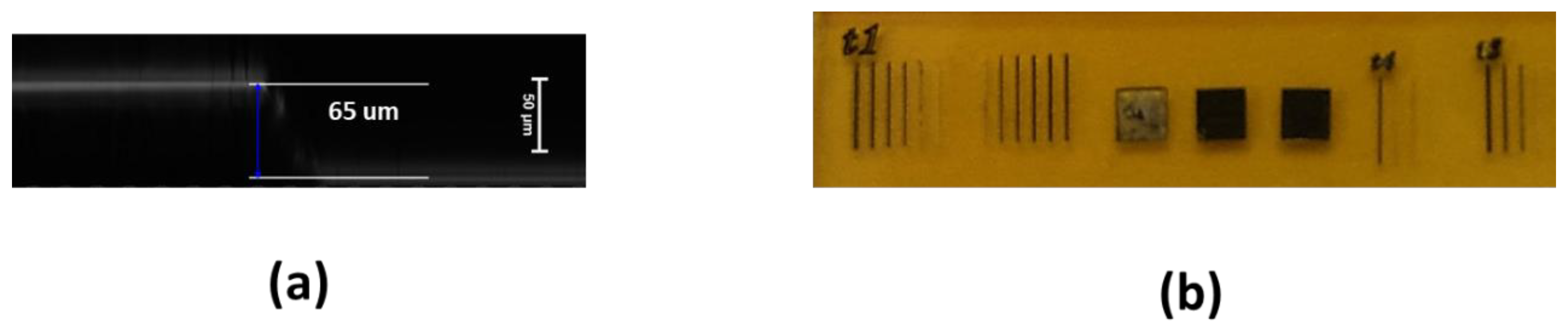
Figure 2.
Loadings Raman spectra used for CLS fitting: graphene (red curve) and PI (blue curve). .
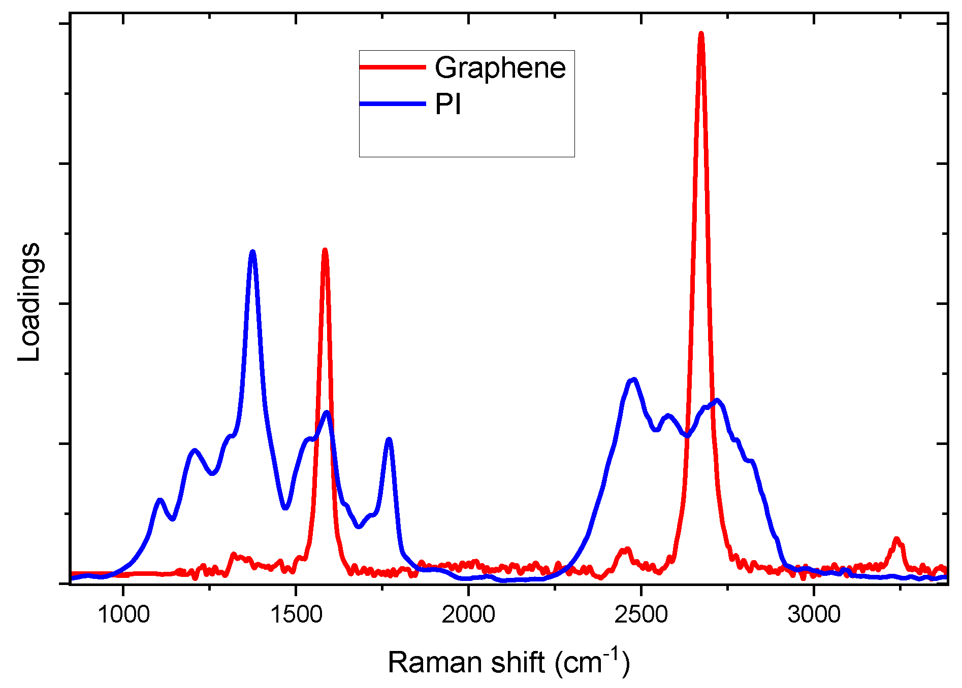
Figure 3.
(a) Upper panel: polyimide structure (credit: Opera propria, CC BY-SA 3.0, https://commons.wikimedia.org/w/index.php?curid=1552614), lower panel: optical images of lines 1, 5, 6, 8 written with UV laser at 5 mm/s, the laser power increases from line 1 to 8; (b) Raman spectra measured from lines 1, 5, 6 and 8 compared with that of Kapton; (c) graphene scores calculated for the Raman spectra of each line. .
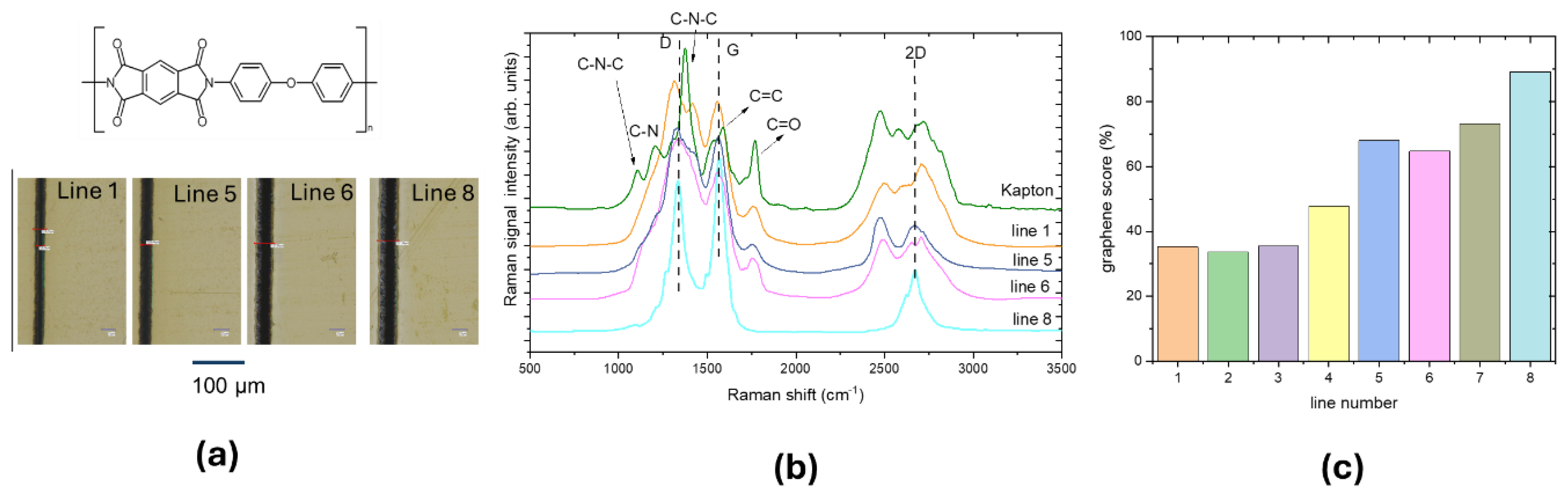
Figure 4.
(a) White light optical images of UV-written LIG squares: Q1_UV, Q2_UV and Q4_UV_KN; (b) upper panel: Raman spectra measured from Q1_UV, Q2_UV and Q4_UV_KN squares, lower panel: graphene scores; (c) Raman maps in false color, the contrasting parameters is the intensity of G peak at 1560 cm-1, normalized respect to the area of whole spectrum. The intensity value increases from brown-red-yellow. .
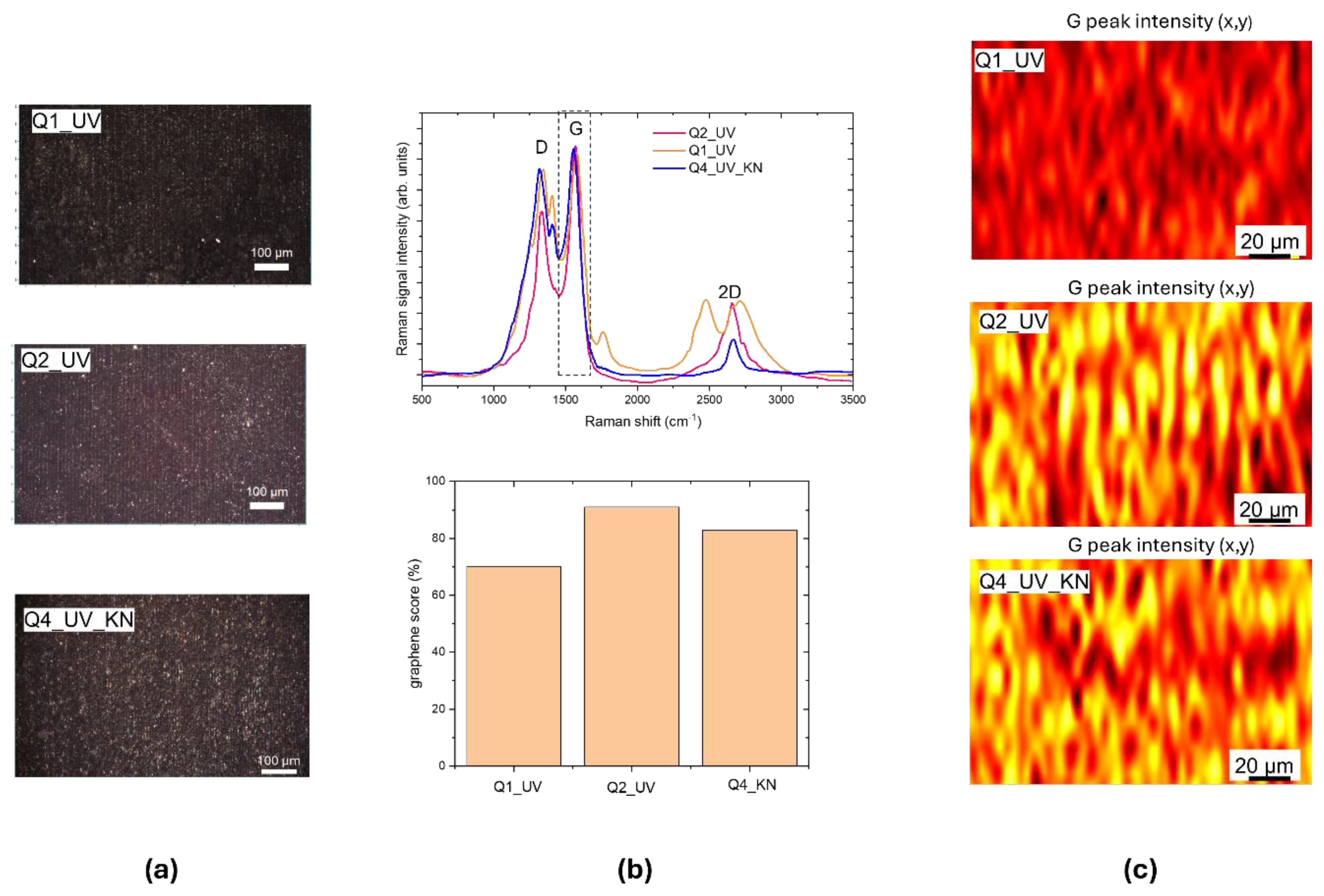
Figure 5.
(a) 3D CLSM image of the LIG square Q2_UV, xy slice = (633x633) µm2, z scanning interval = (0-50) µm. (b) Intensity profile along the yellow arrow of (a). (c) A selected xz slice of (a).
Figure 5.
(a) 3D CLSM image of the LIG square Q2_UV, xy slice = (633x633) µm2, z scanning interval = (0-50) µm. (b) Intensity profile along the yellow arrow of (a). (c) A selected xz slice of (a).
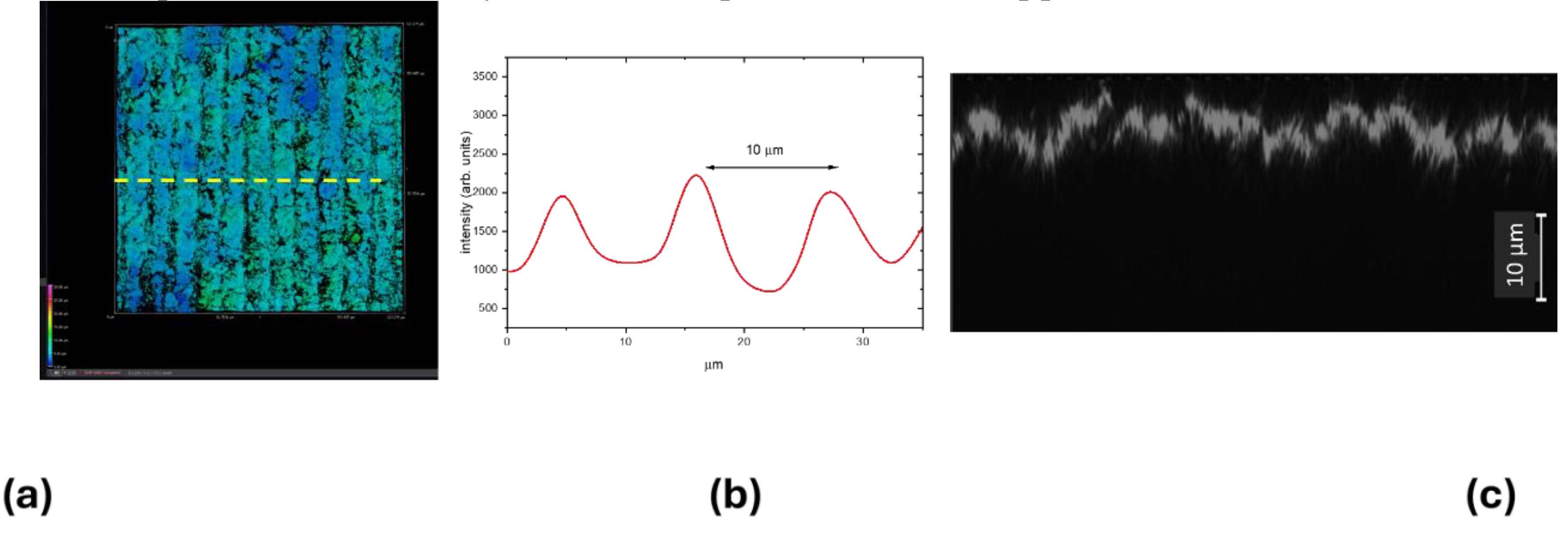
Figure 6.
(a) 3D CLSM image of LIG square Q4_KN, xy slice = (633x633) µm2, z scanning interval = (0-50) µm. (b) Intensity profile along the yellow arrow of (a). (c) A selected xz slice of (a).
Figure 6.
(a) 3D CLSM image of LIG square Q4_KN, xy slice = (633x633) µm2, z scanning interval = (0-50) µm. (b) Intensity profile along the yellow arrow of (a). (c) A selected xz slice of (a).
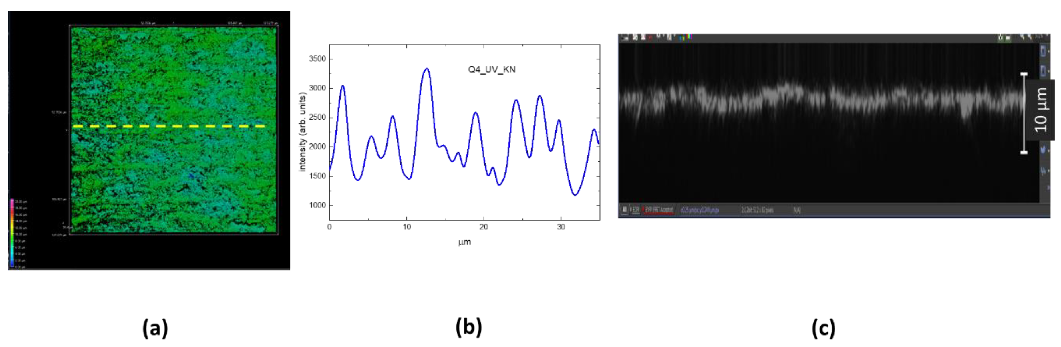
Figure 7.
(a) Raman map of normalized G peak intensity, the color code is brown red, yellow. (b) Intensity profile measured by CLSM of the patterned LIG structures (c) Enlarged view of (a); (d) Raman spectra measured in the yellow (A) and brown (B) regions.
Figure 7.
(a) Raman map of normalized G peak intensity, the color code is brown red, yellow. (b) Intensity profile measured by CLSM of the patterned LIG structures (c) Enlarged view of (a); (d) Raman spectra measured in the yellow (A) and brown (B) regions.
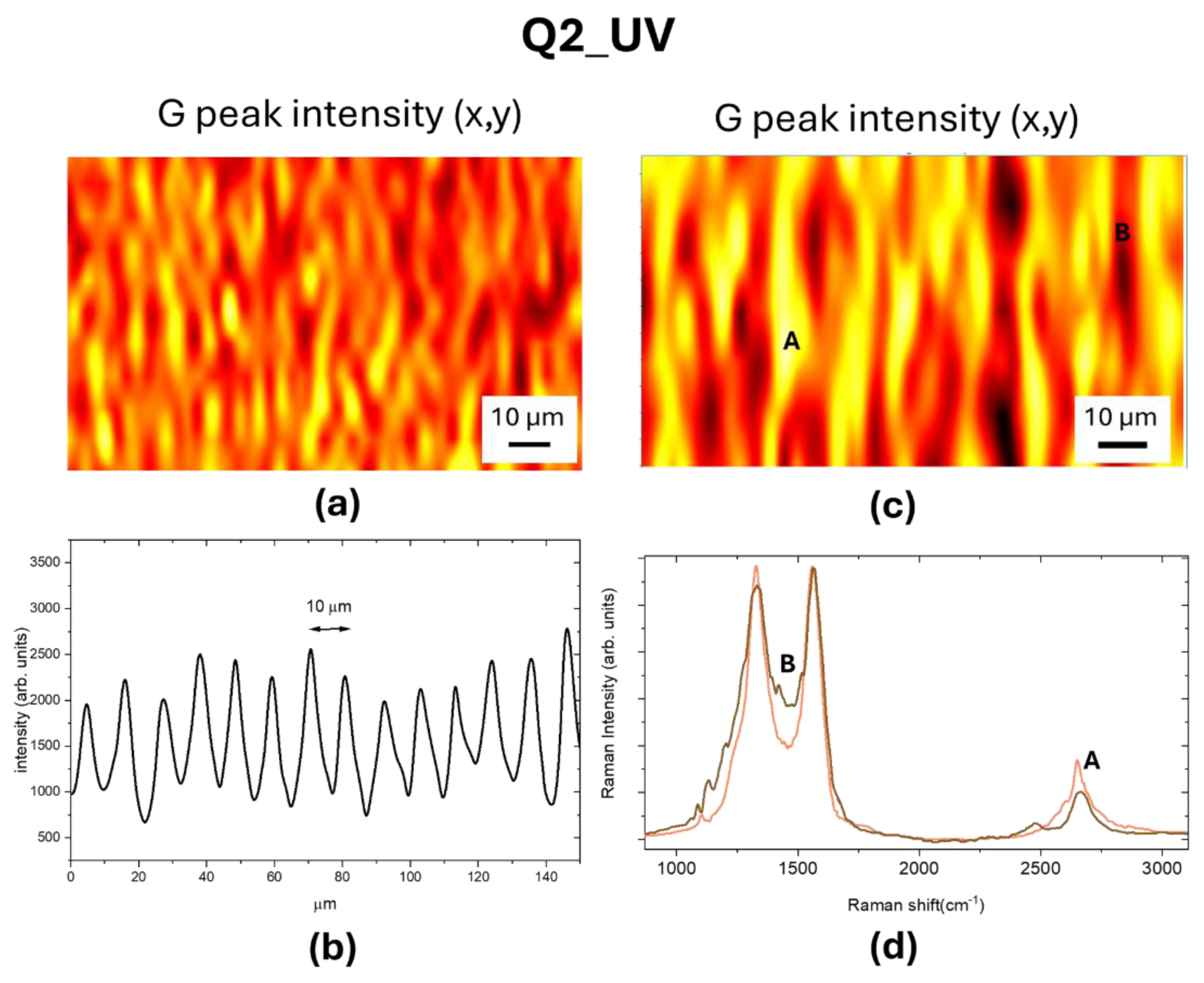
Figure 8.
(a)Topographic AFM image. (b) 3D version of (a). (c) Statistical analysis: height histogram (fuchsia diamonds) acquired from the whole area of the image reported in (b). The height distribution can be fitted by three gaussian functions.
Figure 8.
(a)Topographic AFM image. (b) 3D version of (a). (c) Statistical analysis: height histogram (fuchsia diamonds) acquired from the whole area of the image reported in (b). The height distribution can be fitted by three gaussian functions.
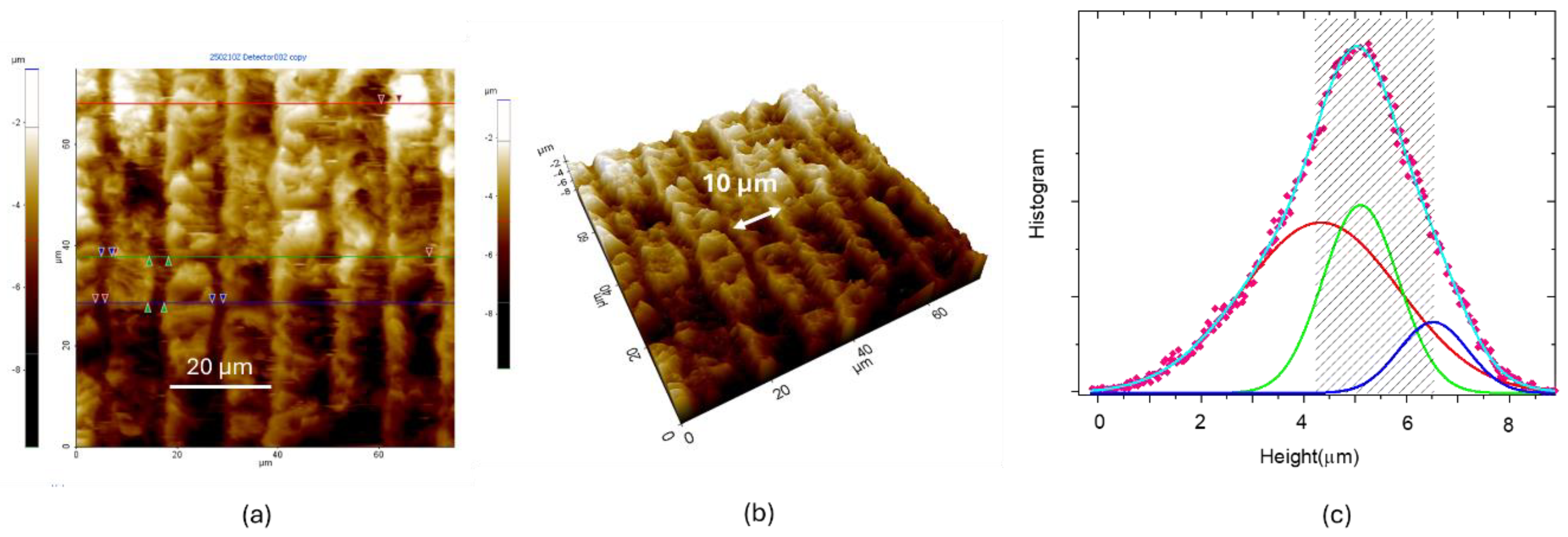
Figure 9.
(a) Raman spectra of CO2 LIG samples. (b) white light optical images of CO2 LIG samples. (c) Raman maps of normalized G peak intensities of samples imaged in (b), the color code is brown, red, yellow.
Figure 9.
(a) Raman spectra of CO2 LIG samples. (b) white light optical images of CO2 LIG samples. (c) Raman maps of normalized G peak intensities of samples imaged in (b), the color code is brown, red, yellow.
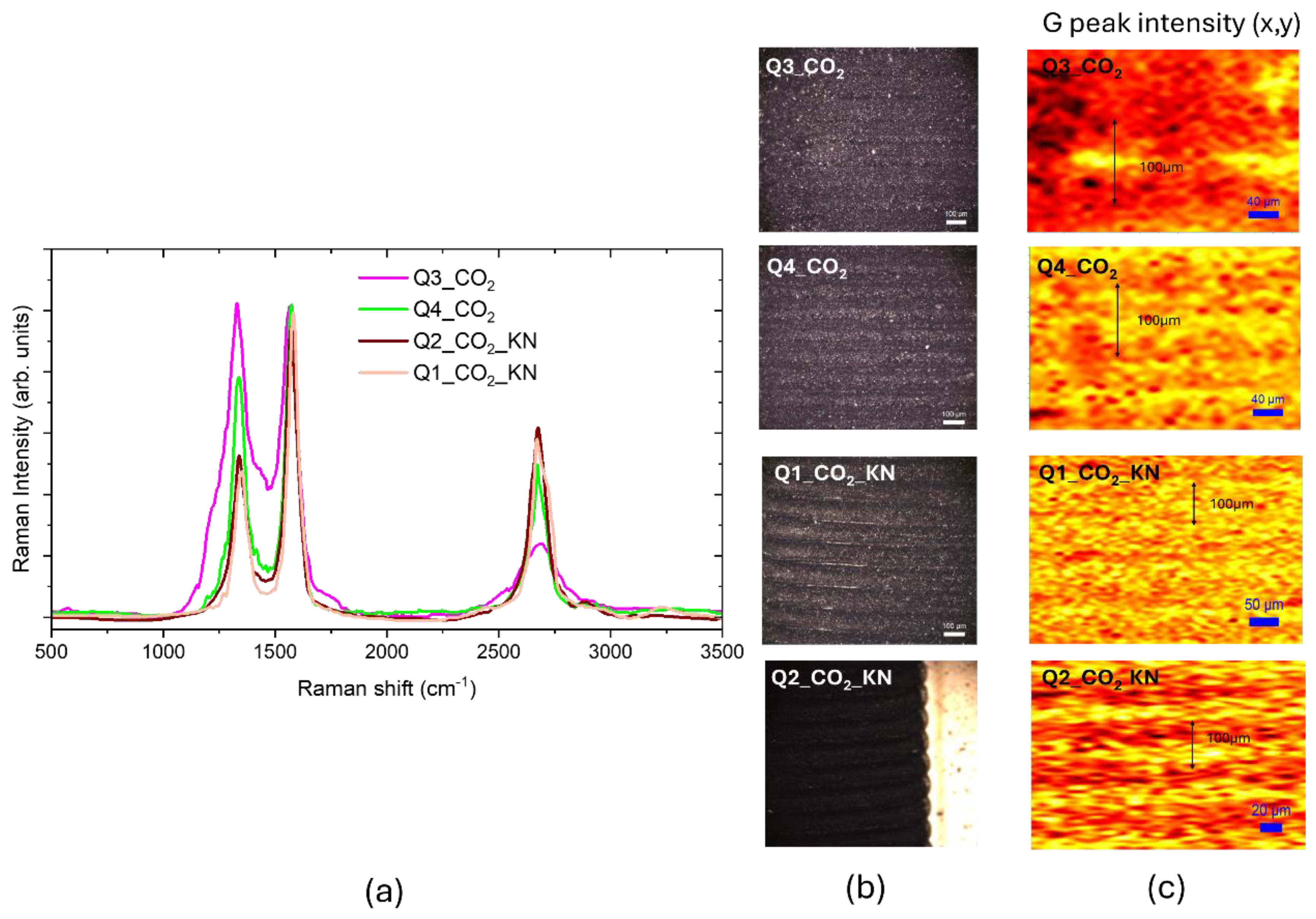
Figure 10.
(a) 3D CLSM image of a corner of the LIG squares Q3_CO2 and Q4_CO2; xy slice = (633x633) µm2, z scanning interval = (0-70) µm. The scale in false colors is from blue (top surface z= 0) to magenta (bottom surface z = 70 µm). (b) xy intensity profiles along dotted horizontal yellow lines of (a). (c) xz slices with the swelling effect measured in the Z direction.
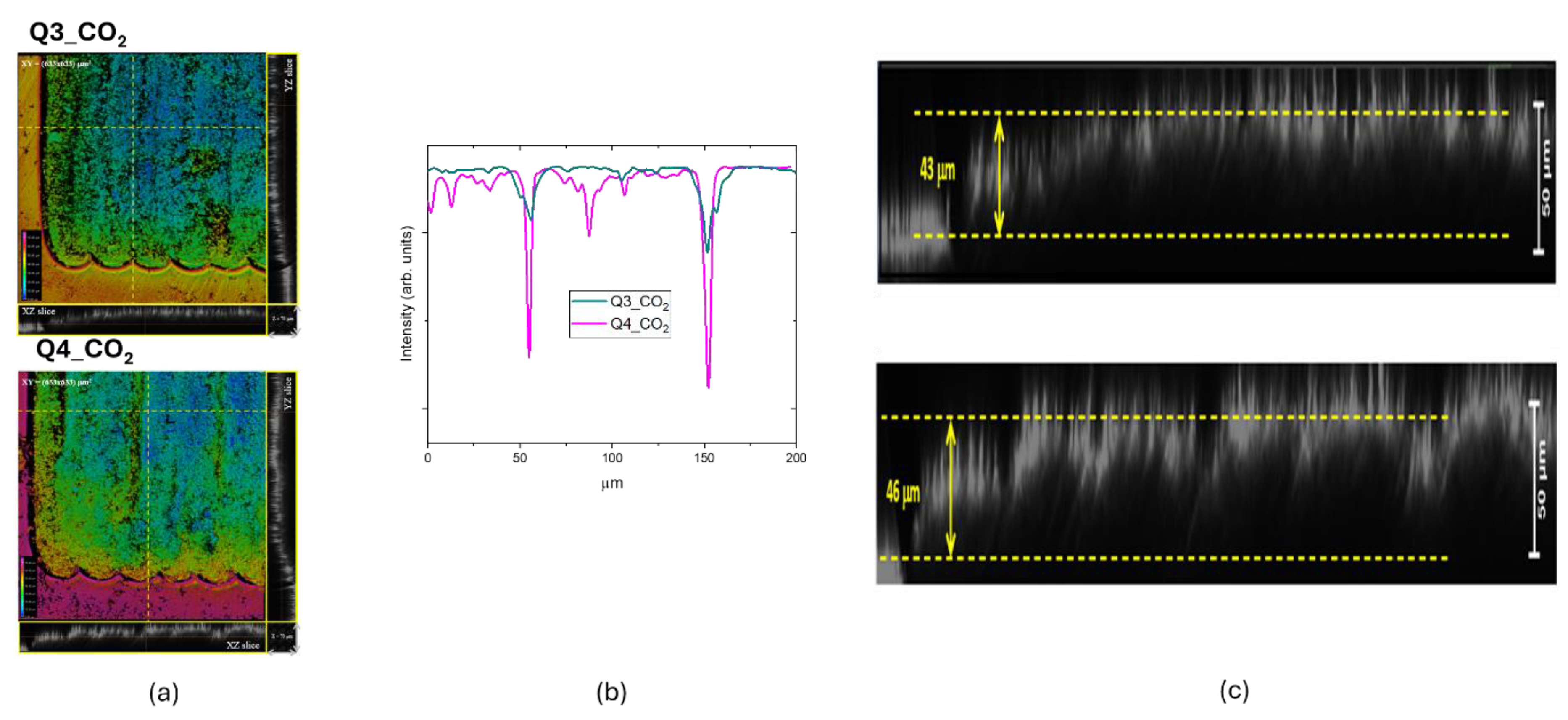
Figure 11.
(a) 3D CLSM images of Q1_CO2_KN and Q2_CO2_KN samples; xy slice = (633x633) µm2, z scanning interval = (0-70). (b) xy intensity profiles along horizontal lines of (a); (c) xz slices with the swelling effect measured in the Z direction.
Figure 11.
(a) 3D CLSM images of Q1_CO2_KN and Q2_CO2_KN samples; xy slice = (633x633) µm2, z scanning interval = (0-70). (b) xy intensity profiles along horizontal lines of (a); (c) xz slices with the swelling effect measured in the Z direction.
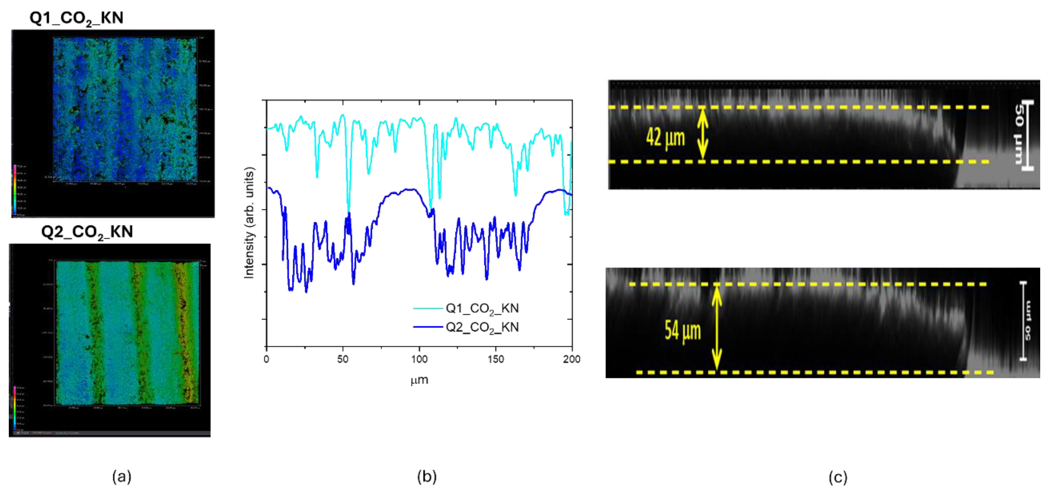
Figure 12.
SEM images of UV LIG square Q2_UV (a) and CO2 LIG square Q1_ CO2_KN (b) at different magnifications.
Figure 12.
SEM images of UV LIG square Q2_UV (a) and CO2 LIG square Q1_ CO2_KN (b) at different magnifications.
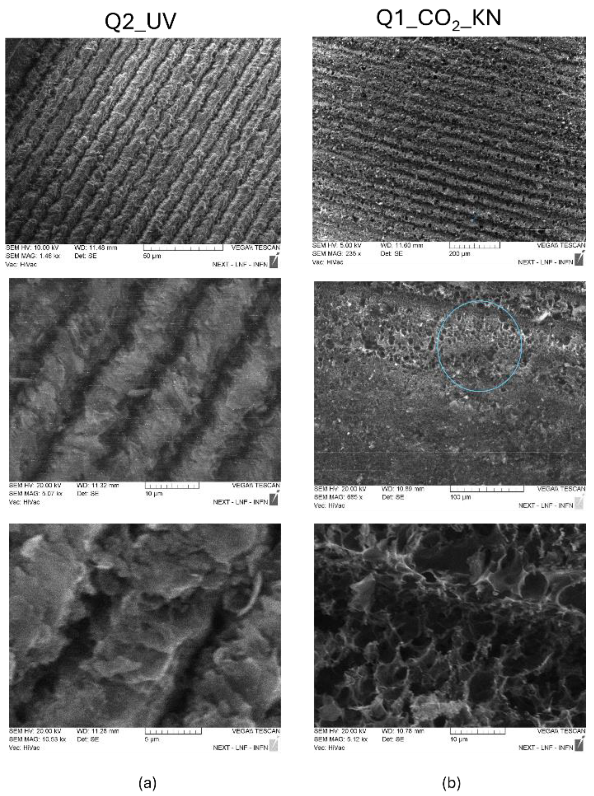
Figure 13.
(a) WCA measured for UV and CO2 LIG samples as a function of graphene score calculated with CLS fitting; (b) WCA measured for UV and CO2 LIG samples as a function of I2D/IG ratio. The dotted line indicates the WCA of CVD graphene.
Figure 13.
(a) WCA measured for UV and CO2 LIG samples as a function of graphene score calculated with CLS fitting; (b) WCA measured for UV and CO2 LIG samples as a function of I2D/IG ratio. The dotted line indicates the WCA of CVD graphene.
Disclaimer/Publisher’s Note: The statements, opinions and data contained in all publications are solely those of the individual author(s) and contributor(s) and not of MDPI and/or the editor(s). MDPI and/or the editor(s) disclaim responsibility for any injury to people or property resulting from any ideas, methods, instructions or products referred to in the content. |
© 2025 by the authors. Licensee MDPI, Basel, Switzerland. This article is an open access article distributed under the terms and conditions of the Creative Commons Attribution (CC BY) license (http://creativecommons.org/licenses/by/4.0/).
Copyright: This open access article is published under a Creative Commons CC BY 4.0 license, which permit the free download, distribution, and reuse, provided that the author and preprint are cited in any reuse.


