Submitted:
17 April 2025
Posted:
18 April 2025
You are already at the latest version
Abstract
The aim of this study is to present the combined effects of total ionizing dose (TID) radiation and electrical stress on the performance of n-MOSFET current mirrors. We propose a novel approach to analyze the complex interaction between these two factors by subjecting devices to different doses of TID and electrical stress. The results indicate that TID radiation gives rise to a threshold voltage shift and degradation in transconductance. Furthermore, we demonstrate that the combined effects of TID and electrical stress lead to a more significant degradation of current mirror characteristics than either stressor alone. These anomalies are explained as due mainly to charge trapping in the oxide layer. The work highlights the importance of considering both TID radiation and electrical stress in designing and qualifying high performance n-MOSFET current mirrors for radiation-hardened environments.
Keywords:
n-MOSFET current mirrors
; Total Ionizing Dose
; Electrical stress
; Threshold voltage
; Current gain
; Input-output impedances
1. Introduction
As semiconductor technology has advanced, integrated circuit (IC) applications revealed a signifying progress and the harsh environment of space has also had a significant impact on device performance. According to statistics performed on satellite failures, a major part is found to be arising from electronic circuits rather than mechanical ones [1,2]. Space radiation poses a significant threat to the reliable operation of electronic circuits, particularly MOS devices. Exposure to radiations can induce single-event (SE) and total-ionizing-dose (TID) effects. While much of the research has focused on SEE effects, there remains a limited body of work addressing the TID mechanisms. An inverter, as a fundamental building block of a MOS circuit [3], is a crucial element to understand the overall system's radiation tolerance. The TID effect is characterized by a cumulative degradation of electronic device performance due to exposure to high-energy rays and charged particles [4,5,6]. It is worth noting that the latter TID mechanism constitutes the main factor limiting the life time of these devices. Opposed to the SEE, the TID effect cannot be completely mitigated. Therefore, a comprehensive analysis of the latter TID effect is essential for assessing the radiation hardness of an integrated circuit. Even at low doses, MOS devices exhibit a higher susceptibility to radiation [7,8,9]. These changes are primarily attributed to the accumulation of positive charges within the oxide layer and the generation of interface traps at the SiO2/Si interface [10,11]. Beyond the immediate impact on device performance, the long-term reliability of devices after exposure to radiation is crucial for ensuring mission success. The device reliability after radiation is important for applications. Knowledge of dependability is also crucial to establish device aging models [12,13,14,15]. Electrical stress exerted on MOS devices can lead to shifts in threshold voltage, degradation in transconductance, and other critical parameter variations [16,17,18,19,20].These changes can have cascading effects, causing failures in both analog and digital circuits. To the subject of biasing, integrated circuits (ICs) require essentially accurate bias voltages and currents for their proper operations [21,22,23]. Traditional CMOS dividers were usually used to realize a suitable biasing. But they again suffer from their dependency on the process technology, supply voltage and temperature [24]. More recently, current mirrors (CMs) have been conceived as new building devices to attain an appropriate biasing. Also, the CMs can amplify or attenuate a current from one location to another in an analog IC
[25,26]. Hence, an efficient design of a CM is mainly to achieve better performance parameters such as current gain, input-output impedances and power consumption.
The present work is aimed to investigate the combined effects of electrical stress and TID on the electrical aging of CMs based on n-MOSFETs. The paper is organized as follows: Section I is dedicated to a brief introduction and related works; Section II presents the electrical aging model for n-MOSFET structures; Section III describes the reliability analyses of TID effects on n-MOSFET current mirrors; Section IV summarizes conclusions and prospects.
2. Electrical Aging Model for n-MOSFETS Structrues
2.1. Hole Trapping
Due to ionizing radiation, the charge build-up into the oxide layer arises from the generation of electron-hole pairs and a subsequent hole trapping. This supposes that de-trapping of holes is neglected. Another simplifying hypothesis can also be adopted. It consists in assuming that the distribution of hole traps is uniform. Which leads to set up the rate equations that govern the trapping of holes as follows :
where ɣ denotes the rate of generation of electron-hole pairs per unit volume, v is the velocity of holes, σ defines the capture cross-section of the trap sites and NTis the density of hole traps throughout the oxide layer. Under this form, it is worth noting that Eqs (1) and (2) can be solved exactly only when the term ɣ is not accounted for. An illustration is given in the report of Ning [27].Later, the charge build-up in MOS structures has been undertaken by Viswanathan [28]. Most interesting, the rate equations were solved for ɣ non null, but in two limiting cases:
i- the density of trapped holes is not large enough compared to the total number of hole traps.
ii- the trapping efficiency is much less lower than the rate of electron-hole generation. The solutions thus adopted in the last case can be combined under a general form:
with { N= ɣ ; =} in the first limiting case and { N=;= }in the second one.
The origin of the x-axis is fixed at the gate-dioxide interface. As has been found, the density of trapped holes shows an exponential amount with a saturated trend going towards the silicon-dioxide interface. In Eq.(3) , can be interpreted as the probability per unit length of a hole to being trapped within the oxide layer under irradiation.
2.2. Time-Dependent Hole Trap Density and Transconductance
Because of hole trapping, a potential shift can occur at the oxide terminal and whose expression versus trapped holes p(x,t) is given by :
where q is the electronic charge, represents the dielectric constant of the oxide layer, is the permittivity of free space, tox is the oxide thickness and FB is a subscript meaning flat band. In evaluating the integral as a function of tox, the mean trapping free length is treated as a parameter. Calculation of under a positive bias voltage leads to the following expression:
with:
For a fixed thickness of the oxide layer and taking the mean trapping free length λ less low than ,the pre-exponential factor N will correspond to the hole trap density NT. On the other hand, by identifying Δ to the threshold potential shift ΔVth (TID) as measured under irradiation, we can derive the TID-dependent oxide trapped charge density from the relation:
To further improve the trapping charge model, it is required to assume the existence of an additional sheet charge near the Si /Si interface,related to surface states or arising from shallow traps .To account for the contribution of all these charge states can be approximately made by defining an effective density of hole traps as: where represents a centesimal percent factor being negative if the additional sheet charge is predominated by electron-traps or positive in the reverse case. Here, this correction is not taken into account.
A deal of interest would also be paid to the transconductance parameter. Let be the gate-to-source bias voltage under gamma radiation. Similarly, to the hole trap density, the time-dependent transconductance is taken under the form:
where ɳ is an empirical factor and gm (TID=0) is the initial transconductance before irradiation. Note, that ɳ can be determined from measured gm (TID) and calculated NT(TID) using the relation:
3. Reliabilityanalyses of Total Ionizing Dose Effects ON n-MOSFET Current Mirrors
3.1. Electrical Aging Behavioral of an n-MOSFET
The n-MOSFET under investigation has been fabricated using 1 µm channel technology. The thickness of oxide layer is fixed at tox=25 nm . More details on the epitaxial growth and the annealing process are available in Ref [29].
Concerning VGS-IDS characteristics, measurements were performed before and after irradiation for VDS fixed at 50 mV in the linear regime and VDS=3V in the saturation regime. As it is seen, the threshold potential shows a negative shift with increased TID and the relevant data are found to be fitted by the polynomial law:
where Vth (TID=0)=1.69Volt.From measured ΔVth(TID),we have deduced the density NT of induced hole traps as a function of TID using Eq(6). The mean trapping free length is fixed at =5nm which corresponds to . Results are depicted in Fig.1, on an interfacial charge plot .It clearly appears that the trapping of holes shows a gradual amount as the total ionizing dose increases. As has also been provided, the interfacial density of hole traps is related to TID by the fitting relation :
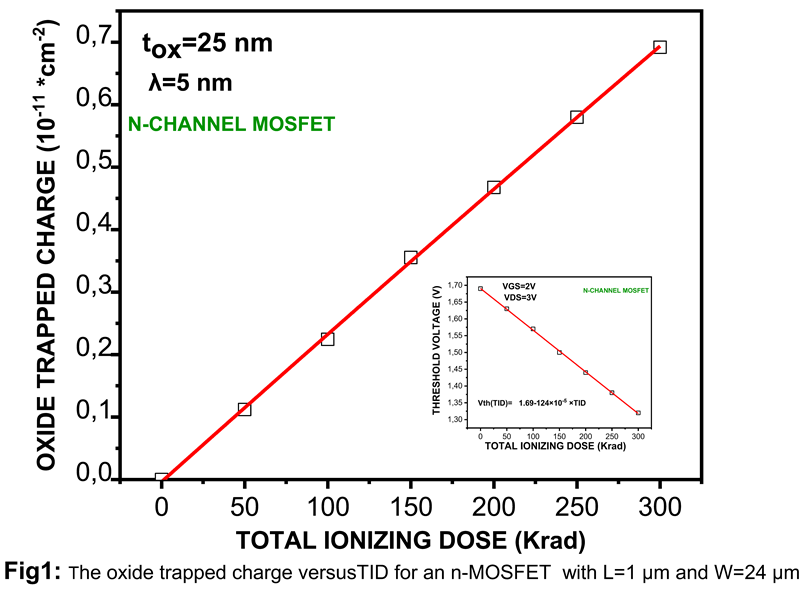
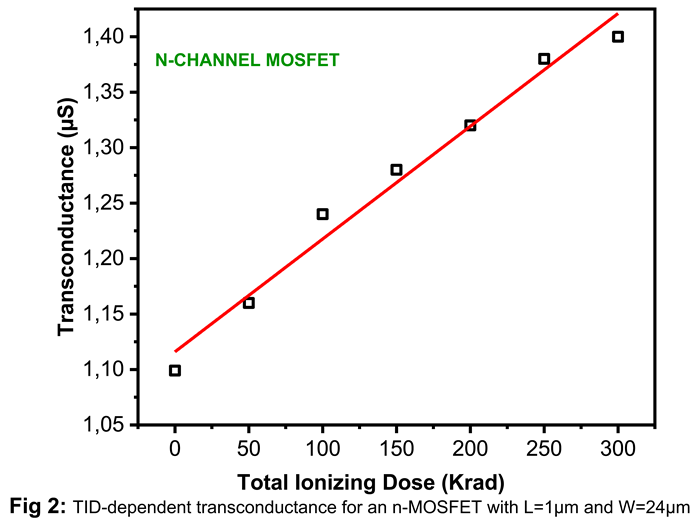
In addition to NT, the graph shows the corresponding threshold potential versus TID.As a proposal of explanation, exposure to relatively high TID levels induces defects in the MOS capacitance. Which can make it difficult for electrons to flow into the conductive channel. Microscopically, an accumulation of holes reduces switching speed of the MOSFET. As a peculiar feature, the threshold potential shift is found to be more significant at lower TID doses. Additionally, an increase in the threshold voltage can enhance the power consumption. Another fundamental parameter of the n-MOSFET that is impacted by gamma radiation consists in then transconductance. Measurements of this parameter have led to an increasing trend versus TID. The data points are depicted in Fig.2 with the obtained fitting:
From measured gm (TID) and NT (TID),we have computed the empirical factor ɳ (TID).Results are found to be fitted by:
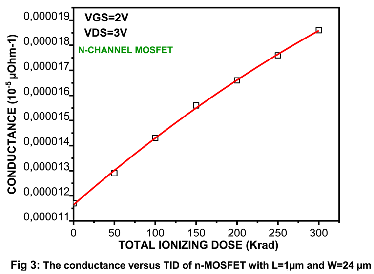
For the conductance, however, how we did make in relating this parameter to the charge built-up into the oxide. Calculation has been made using TID as an auxiliary variable, which has led to the plot of Fig.3. As can be noticed, the conductance increases with TID according to the fitting:
3.2. Electrical Degradation Mechanisms in n-MOSFET Current Mirrors
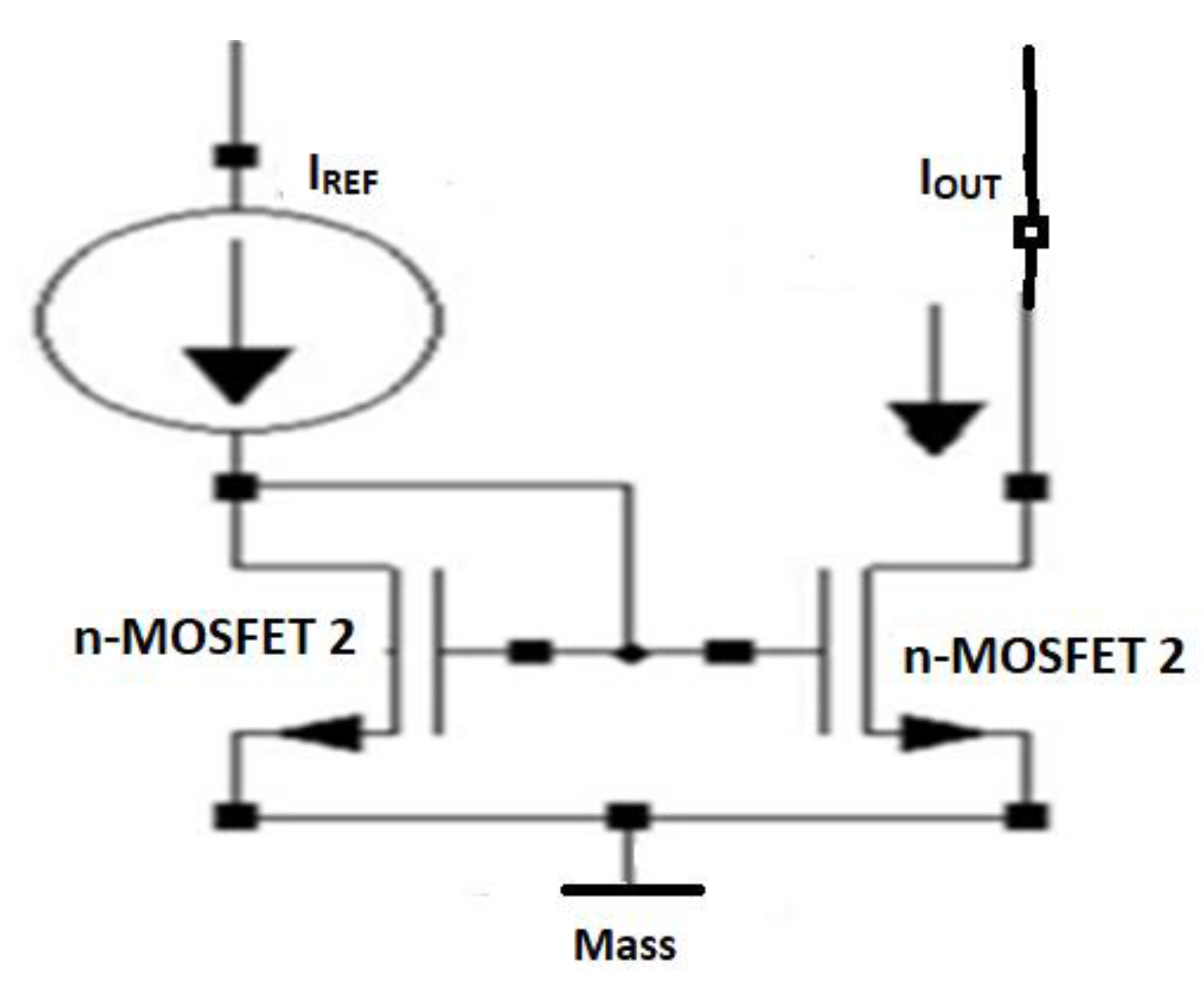
The biasing CM as it used in AMS integrated circuits [29] is shown in Fig.4 with its dynamical equivalent scheme. It is constructed using two n-MOS transistors labelled M1 et M2.The diode-connected transistor M1 operates in saturation regime and converts the reference current IREF into a corresponding gate-to-source voltage VGS1. The transistor M2 is a regenerating module that gives rise to an output current IOUT. If both the transistors M1 and M2 are matched, the gate-to-source biases VGS1 and VGS2 are equal and then IREF would be perfectly at the output of CM. Under saturation conditions, the reference and output currents are given by the set of electrical equations:
 where µn is the electron mobility, Cox denotes the MOSFET capacitance per unit area and VTHi =1.2 are the threshold potentials of the n-MOSFETs. From IREF and Iout , we can derive the current gain. It is undoubtedly that this parameter is affected by irradiation. Let TID1=x TID and TID2= (1-x)TID with 0≤ x ≤1 be the total ionizing doses for the MOSFET1and MOSFET2 transistors respectively. The current gain of the SCM reads as:
where x represents a dissymmetric percent that characterizes the TID contamination of the n-MOSFETs. Calculation of AiSCM(x.TID) has led to a graph of the current gain of an n-MOSCM versus x for different TIDs as illustrated in Fig.5. We note that the current gain is a measure of how much an n-MOSFET mirror can replicate a current signal. The plot also shows that the current gain decreases as TID increases. This is because exposure to ionizing radiations damages the MOSFET’s gate oxide and reduces the ability of the gate to control the flow of current between the source and drain. As a further observation, the decreasing rate in current gain is found to change with the dissymmetric percent. Analytically, the x- and TID- dependent current gain are fitted according to:
where µn is the electron mobility, Cox denotes the MOSFET capacitance per unit area and VTHi =1.2 are the threshold potentials of the n-MOSFETs. From IREF and Iout , we can derive the current gain. It is undoubtedly that this parameter is affected by irradiation. Let TID1=x TID and TID2= (1-x)TID with 0≤ x ≤1 be the total ionizing doses for the MOSFET1and MOSFET2 transistors respectively. The current gain of the SCM reads as:
where x represents a dissymmetric percent that characterizes the TID contamination of the n-MOSFETs. Calculation of AiSCM(x.TID) has led to a graph of the current gain of an n-MOSCM versus x for different TIDs as illustrated in Fig.5. We note that the current gain is a measure of how much an n-MOSFET mirror can replicate a current signal. The plot also shows that the current gain decreases as TID increases. This is because exposure to ionizing radiations damages the MOSFET’s gate oxide and reduces the ability of the gate to control the flow of current between the source and drain. As a further observation, the decreasing rate in current gain is found to change with the dissymmetric percent. Analytically, the x- and TID- dependent current gain are fitted according to:
Figure 4.
The basic n-MOSET current mirror circuit SCM.
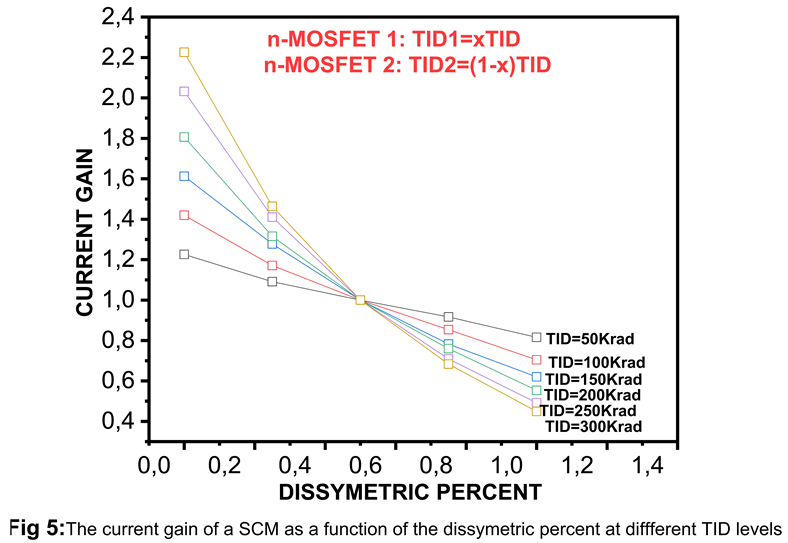
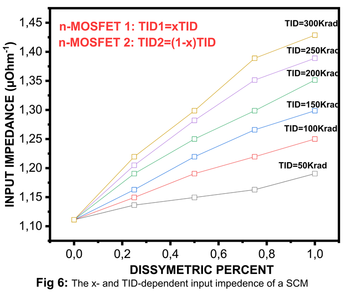
Usually concerning the dissymmetric percent, it is worth to notice that a relatively high value of this coefficient means that the n-MOSFET gate-oxide becomes more asymmetric. This makes it sufficiently susceptible to submit damages from ionizing radiation. Two other important parameters were dialed with an interest. They consist in input and output impedances of the SCM. According to that TD1 and TD2 were defined above, both impedances read under the forms:
Using Eq.18 and Eq.19, we have calculated and versus x for different TIDs ranging from 50 Krad to 300 Krad. As can be seen, Fig.6 shows a clear positive correlation between the dissymmetric percent and input impedance, independently on the TID level. Such an increasing in impedance is assigned to the disruption of conduction paths caused by asymmetry. Moreover, the effect of TID is significant, suggesting that defects created by radiation also reinforce the CM resistance at input. The graph of Fig.7, however, shows how the output impedance is affected by the two factors. As it is seen, the impedance at output decreases with increased asymmetry percentage and total ionizing dose. In terms of analytical fitting of and , it is provided by the following set of expressions:
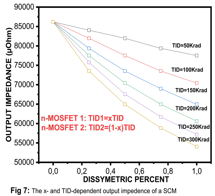
In a concluding remark, input and output impedances of a perfect current mirror should be very low and large enough respectively. This suggests that degradations induced by geometric dissymmetry and the effect of ionizing radiation, have a negative impact on CM’ ability to deliver more current to the load. It is then required to characterize these degradations in an attempt to develop an equivalent model that includes the parameter related to a radiation-hardened environment. In practice, SCMs are suitable for low voltage applications. Technologically, the limited usage of SCMs is contributed to their low output impedances. Some remedies were conceived to further improve the impedance at output. They consisted in widlar CM [26] and cascade CM [25,26] designs. As has been found, the output impedance of a SCM is increased due to Widlar and Cascade arrangements with respective ratios.
In closing this subsection, it is worth to mention that the cascade technology can open a promising way to construct electronic applications with low voltage operation and low power consumption. But the use of complexed configurations needs a multitude of elementary transistors. Because of different operating regimes, the cascade CMs could exhibit a mismatching in current and voltage between input and output. Exposure to ionizing radiations would lead to further degradations as well.
4. Conclusions
In this study, we have investigated the combined effects of TID radiation and electrical stress on the performance of current mirrors based on n-MOSFETs. Through experimental measurements and simulations using LTspice, we analyzed both TID radiation and electrical stress independently contribute to a degradation of the current mirror's accuracy, matching, and electrical performance. Our results demonstrate that both TID radiation primarily causing charge trapping in the gate oxide leading to a threshold voltage shift, while electrical stress provokes these effects by a further altering device characteristics such as transconductance and current gain. Consequently, current mirrors subjected to both TID radiation and electrical stress show significant changes in their characteristics, leading to a loss of precision and reliability. The findings highlight the importance of considering both radiation and electrical stress in the design and qualification of n-MOSFET current mirrors for radiation-hardened applications. To mitigate these effects, it is essential to explore design optimizations such as improved radiation-hardened materials, fault-tolerant circuit topologies, and enhanced device shielding techniques. Further research should focus on developing a complete model to predict the combined impact of TID radiation and electrical stress. This undoubtedly allows to design more accurate MOSFET-circuits against high gamma-ray doses.
References
- Zhang, S.; Shi, J.; Wang, J.L. Satellite on-board failure statistics and analysis. Space cr. Eng. 2010, 19, 4l–46. [Google Scholar]
- Cao, Y.; Wang, M.; Zheng, X.; Zhang, E.; Lv, L.; Wang, L.; Ma, M.; Lv, H.; Wang, Z.; Wang, Y.; et al. Combined Effect of TID Radiation and Electrical Stress on NMOSFETs. Micromachines 2022, 13, 1860. [Google Scholar] [CrossRef] [PubMed]
- Gao, T.; Yin, C.; Chen, Y.; Chen, R.; Yan, C.; Liu, H. Simulation of Total Ionizing Dose Effects Technique for CMOS Inverter Circuit. Micromachines 2023, 14, 1438. [Google Scholar] [CrossRef]
- Bonaldo, S. TID effects in highly scaled gate-all-around Si nanowire CMOS transistors irradiated to ultra-high doses. IEEE Trans. Nucl. Sci. 2022, 69, 1444–1452. [Google Scholar] [CrossRef]
- Wang, S. Research and Modeling of Irradiation Characteristics of Ultra-Deep Submicron Devices. Ph.D. Thesis, Changchun University of Technology, Changchun, China, 2010. [Google Scholar]
- Zeng, C.; Li, X.; Gao, L. Research on High Temperature Characteristics of 28 nm Ultra-Thin FDSOI. Microelectronics 2021, 51, 577–581. [Google Scholar]
- Nasr, A.; Ashour, M. Experimental Studies for the Evaluation of Non-Ionizing Radiation Levels”, The Second All African IRPA Regional Radiation Protection Congress, 223 (2007).
- Nasr, Effect of ionizing radiation on the characteristics of photodetectors, The Second All African IRPA Regional Radiation Protection Congress, 231(2007).
- Prakash, G.; Ganesh, P.; Nagesha, Y.N.; Umakanth, D.; Arora, S.K.; Siddappa, K. Effect of 30 MeV Li3+ ion and 8 MeV electron irradiation on N-channel MOSFETs. Radiation Effects and Defects in Solids 2002, 157, 323–331. [Google Scholar] [CrossRef]
- Oldham, T.R.; Mclean, F.B. Total ionizing dose effects in MOS oxides and devices. IEEE. Trans. Nucl. Sci. 2003, 50, 483–499. [Google Scholar] [CrossRef]
- Schwank, J.R.; Shaneyfelt, M.R.; Fleetwood, D.M.; Felix, J.A.; Dodd, P.E.; Paillet, P.; Cavrois, V.F. Radiation effects in MOS oxides. IEEE. Trans. Nucl. Sci. 2008, 55, 1833–1853. [Google Scholar] [CrossRef]
- Grasser, T. Stochastic charge trapping in oxides: From random telegraph noise to bias temperature instabilities. Microelectronics Reliability 2012, 52, 39–70. [Google Scholar] [CrossRef]
- Guérin, C.; Huard, V.; Bravaix, A. General framework about defect creation at the Si/SiO2 interface. Journal of Applied Physics 2009, 105, 114513. [Google Scholar] [CrossRef]
- Rauch, S.E.; La Rosa, G. The energy-driven paradigm of NMOSFET hot-carrier effects. IEEE Transactions on Device and Materials Reliability 2005, 5, 701–705. [Google Scholar] [CrossRef]
- Tyaginov, S.; Jech, M.; Franco, J.; Sharma, P.; Kaczer, B.; Grasser, T. Understanding and Modeling the Temperature Behavior of Hot-Carrier Degradation in SiON nMOSFETs. IEEE Electron Device Letters 2016, 37, 84–87. [Google Scholar] [CrossRef]
- Zhicheng Wu, Jacopo Franco, Brecht Truijen, Philippe Roussel, Stanislav Tyaginov, Michiel Vandemaele1 , Erik Bury, Guido Groeseneken1 , Dimitri Linten, Ben Kaczer. Physics-based device aging modelling framework for accurate circuit reliability assessment.2021.
- Schroder, D.K.; Babcock, J.A. Negative bias temperature instability: Road to cross in deep submicron silicon semiconductor manufacturing. J. Appl. Phys. 2003, 94, 1–18. [Google Scholar] [CrossRef]
- Ullmann, B.; Jech, M.; Tyaginov, S.; Waltl, M.; Lllarionov, Y.Y.; Grill, A.; Puschkarsky, K.; Reisinger, H.; Grasser, T. The impact of mixed negative bias temperature instability and hot carrier stress on single oxide defects. IEEE. Inter. Reliab. Phys. Symp. 2017, XT-10.1–XT-10.6. [Google Scholar]
- Jech, M.; Ullmann, B.; Rzepa, G.; Tyaginov, S.; Grill, A.; Waltl, M.; Jabs, D.; Jungemann, C.; Grasser, T. Impact of mixed negative bias temperature instability and hot carrier stress on MOSFET characteristics—Part II: Theory. IEEE. Trans. Elec. Dev. 2019, 66, 241–248. [Google Scholar] [CrossRef]
- Zhou, X.J.; Fleetwood, D.M.; Felix, J.A.; Gusev, E.P.; Emic, D. Bias-temperature instabilities and radiation effects in MOS devices. IEEE. Trans. Nucl. Sci. 2006, 52, 2231–2238. [Google Scholar] [CrossRef]
- Zhao, X.; Gan, P.; Zhao, Q.; Liang, D.; Cao, Y.; Pan, X.; Bermak, A. A 124 fj/Bit cascode current mirror array based PUF with 1.50% native unstable bit ratio. IEEE Transaction on Circuits and Systems – I: Regular papers 2019, 66, 3494–3503. [Google Scholar] [CrossRef]
- Qin, Z.; Shintani, M.; Kuribara, K.; Ogasahara, Y.; Sato, T. Organic 2020, 20, 7569–7578.
- Lin, Z.; Fang, Y.; Peng, C.; Lu, W.; Li, X.; Wu, X.; Chen, J. Current mirror based compensation circuit for multi-row read inmemory computing. Electron. Lett. 2019, 55, 1176–1178. [Google Scholar] [CrossRef]
- F. Maloberti, Analog Design for CMOS VLSI Systems., International edition Springer, 2007.
- A.S. Sedra, K.C. Smith, and A.N. Chandokar, Microelectronic Circuits – Theory and Applications. Oxford University press, 2013.
- T.C. Carusone, and A. David, Analog Integrated Circuit Design, Wiley Student edition, 2015.
- Ning, T.H. Capture cross section and trap concentration of holes in siicon dioxide. J. Appl. 1976, 47, 1079–1081. [Google Scholar] [CrossRef]
- Viswanathan, C.R.; Maserjian, J. Model for thickness dependence of radiation charging in MOS structures. IEEE Trans. Nucl. Sci 1540, Ns-23, 1540–1545. [Google Scholar] [CrossRef]
- Sedki, A.; André, N.; Kilchytska, V.; Tounsi, F.; Mezghani, B.; Gérard, P.; Ali, Z.; Udrea, F.; Flandre, D.; Francis, L. In situ-Thermal Annealing of On-Membrane SOI Semiconducteur-Based Devices After High Gamma Dose irradiation. Nanotechnology 2017, 28, 184. [Google Scholar]
Disclaimer/Publisher’s Note: The statements, opinions and data contained in all publications are solely those of the individual author(s) and contributor(s) and not of MDPI and/or the editor(s). MDPI and/or the editor(s) disclaim responsibility for any injury to people or property resulting from any ideas, methods, instructions or products referred to in the content. |
© 2025 by the authors. Licensee MDPI, Basel, Switzerland. This article is an open access article distributed under the terms and conditions of the Creative Commons Attribution (CC BY) license (http://creativecommons.org/licenses/by/4.0/).
Copyright: This open access article is published under a Creative Commons CC BY 4.0 license, which permit the free download, distribution, and reuse, provided that the author and preprint are cited in any reuse.


