Submitted:
27 March 2025
Posted:
27 March 2025
You are already at the latest version
Abstract
Automatic techniques for analog integrated circuit layout design have been proposed in the literature for over four decades. However, as analog design moved into deep nanometer integration nodes, the increasing number of design rules, layout-dependent effects influence, congestion, and parasitic structures impact is constantly challenging existing automatic layout generation techniques and keeping pressure on their further improvement. At the time of writing, no automatic tool or flow has established in the industrial environment, resulting in a time-consuming and difficult-to-reuse design process. However, very recently, machine and deep learning techniques started to offer solutions for problems not dealt with in the previous generation of automatic layout tools and are reshaping analog design automation. Therefore, this paper conducts a review of most recent analog integrated circuit automatic layout techniques powered by machine and deep learning methods, covering placement, routing, and trends on post-layout performance estimation, providing an actual, complete and comprehensive guide for circuit designers and design automation developers.
Keywords:
Integrated Circuits
; Automatic Layout Generation
; Electronic Design Automation
; Placement
; Routing
; Performance-Driven Synthesis
; Post-Layout Regressor
1. Introduction
In recent decades, the integrated circuit (IC) industry has experienced remarkable growth, evolving into a multi-billion-dollar sector driven by the surging demand for consumer electronics, which depend heavily on sophisticated systems-on-a-chip (SoCs). While digital signal processing and memory components are essential for the functioning of these SoCs, analog interfaces like wireless communication circuits and sensors are equally critical for enabling interaction with the external world. Although electronic design automation (EDA) tools for digital and memory block design are well-established, the design and layout of analog circuits remain a challenging, error-prone task. With designers relying on traditional computer-aided design (CAD) tools, including schematic editors, simulators, and verification tools, in a repetitive, manual process. Nonetheless, tools and techniques to automate its design process have been vastly proposed by the analog EDA research community for more than four decades, still, there is no established automatic tool or flow in the industrial environment, resulting in a time-consuming and difficult-to-reuse design process. However, recent advances in machine and deep learning (M/DL) have opened new opportunities in the automation of the analog IC design flow, where part of the path has already been paved, such as in device, circuit and system-level modeling, automatic synthesis techniques or even testing [1,2,3,4].
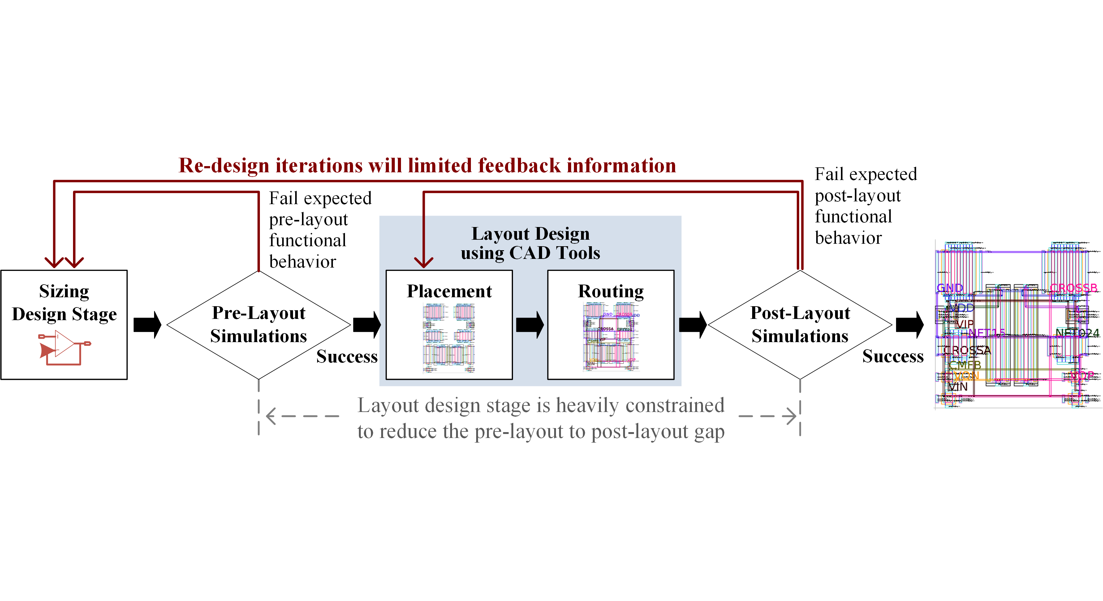
This paper reviews the most recent M/DL efforts applied to automatic analog IC layout generation, which is the task of the analog design flow that both lays the devices out in the chip (i.e., placement), and after, interconnects them (i.e., routing). It is important to note that as analog IC design moved into modern deep nanometer technology nodes, the growing topological requirements, additional process design kit (PDK)’s rules, congestion, and parasitic structures that arise from the physical layout description are continuously defying existent EDA tools. In particular, layout parasitic structures and layout-dependent effects (LDEs) if not adequately weighted during layout design, have been proved to drive analog ICs from promising pre-layout performances to completely malfunction. Hence, their real impact can only be known after complete layout extraction and post-layout simulation, as illustrated in Figure 1. Still, this layout design flow suffers from expensive and time-consuming redesign iterations with limited feedback information to correct the problem. Layout generators powered by novel M/DL techniques are opening new perspectives for developing solutions that simultaneously incorporate legacy data or expert design insights in a manner that was not possible in the previous generations of EDA tools, and therefore, are covered in this review.
This paper is organized as follows: Section 2 presents the most recent advances in neural network-based and reinforcement learning (RL)-based placement; Section 3 shows the improvements on routers enhanced by routing probability maps generated by M/DL, and also, net ordering and track-assignment techniques; Section 4 discusses the preliminary developments on post-layout performance estimation; and, Section 5 summarizes the topics covered on this review.
2. Placement
The analog IC placement consists of determining the positions for the devices of a given circuit/system topology. The task is conducted taking simultaneously many requirements into consideration in order to reduce the unwanted impact of layout parasitic structures, process variations and different on-die operating conditions. Those requirements, which traditionally appear in the form of device symmetry, matching and proximity constraints, among others, allied to the multitude of possible device implementations, with different sizes and aspect ratios, make the analog placement task hard to automate. Furthermore, these constraints must be strictly satisfied while attempting to minimize several objectives, such as chip area or interconnect length estimates, as most of the parasitic effects and consequent performance degradation of the circuit post-layout and the attainable routing quality are set once a placement solution is fixed. For these reasons, automatic analog placement has been an intensive research topic in the research community [5,6].
2.1. A Summary of Traditional Automatic Approaches
Traditional approaches for automating analog IC placement can be categorized into three main types: (1) constrained optimization, where an optimization method, typically using simulated annealing (SA), is applied to adjust the positions of the devices either explicitly or implicitly, with the goal of minimizing specific performance metrics. In the explicit approach, where absolute coordinates are used, each device is defined by its position on a plane without a grid [7,8,9]. This method can represent all possible placements and is the most practical for enforcing topological constraints, as these can be directly implemented using the device coordinates. However, the algorithm must search through both feasible and infeasible solutions, since overlaps between devices may occur. In the implicit approach, where relative positions are employed, the optimizer modifies a structure that represents the layout, and a packing procedure then converts this relative representation into a complete floorplan, while preventing overlaps and ensuring that the necessary topological constraints are satisfied. In this case, the search space is restricted to feasible solutions only. However, implementing topological constraints can be more challenging, as each time the optimizer alters the structure, it must re-evaluate and adjust the layout to address any violations or fixes needed. These discrete operations complicate the original simplicity of relative representations, still notable implementations can be found for the: ordered tree (O-tree) [10], binary tree (B*-tree) [11,12,13], transitive closure graph (TCG) [14,15], hierarchical B*-tree [16], QB-Tree [17] and sequence-pair (SP) [18,19,20,21,22]. Both the explicit and implicit methods do not take into account any previously created layouts, meaning they do not utilize any legacy data; (2) retargeting from an existing design or template involves using the design patterns from a prior floorplan to recreate the same circuit topology, but with new device sizes or integration technology [23,24]. A generic template, independent of technology or specifications, can also be employed to represent these design patterns, with fast compaction techniques applied to produce the updated solution [25]; and (3) knowledge mining takes a different approach by using a collection of legacy layouts instead of just one. In this case, the generated solution doesn’t have to match a specific topology from the legacy data but can be derived from the design patterns of various sub-circuits identified in the library [26].
2.2. M/DL Advances: Neural Network-Based
A preliminary proposal for using M/DL in automating the placement of analog ICs was introduced in [27], where mean-field neural networks were utilized to represent planes with grids for device placement. The problem was framed as a network consisting of multiple parallel planes, one for each device in the circuit. Each plane’s dimensions matched the discrete space available for placing the devices. The grid's edges acted as neurons, and an active neuron indicated the bottom-left coordinate of a device corresponding to its plane. The model optimized an energy function, which penalized issues like device spacing, overlap, symmetry violations, proximity rule breaches, and out-of-bounds placements. These models were topology-dependent, and the discrete space structure makes the model's framework inherently reliant on the dimensions of the devised plane. On a different trail, artificial neural networks (ANNs) were employed to study the design patterns of thousands of validated placement solutions for a single topology [28]. These placements varied while still meeting symmetry and current-flow requirements, with the goal being to train the model to recognize and apply these design patterns to new size scenarios. The output of the network was the position of each of the circuit’s devices in an ℝ² plane, and it was trained to minimize the mean squared error (MSE) between the predicted floorplan and its corresponding solution from the training set. As shown in Figure 2, the model outputted three different floorplans, i.e., one for minimum area, minimum width and minimum height, when requested with a different set of design variables and cells’ physical details.
An improved approach can be found in DeepPlacer [29,30], which uses an ANN trained in a semi-supervised manner and evaluated with a topological constraint satisfaction loss function. Instead of comparing the predicted placements with legacy data, this method assesses whether the placements meet the specified constraints, encouraging new yet accurate behaviors. The study also introduced circuit topology encodings by embedding the topological constraints into the input layer of the ANN using directed graphs, as illustrated in Figure 3. This enabled the model to be applied to various circuit topologies, allowing for knowledge reuse across different designs. However, the model’s limitations include its inability to account for the data structure, restricting it to a fixed maximum number of devices. Additionally, the model's dependence on the order in which devices were fed into it made its real-world application challenging. To address the limitations of encoding circuit characteristics in the input layer, Graph2Seq [31] employed modern embedding methods and a fully unsupervised attention-based encoder-decoder model for automating the analog IC layout placement task. By using a graph-structured input, the model became independent of the device order and scalable, allowing it to handle circuits with more devices than those it was trained on. The graph structure represented placement constraints, not the circuit’s connections, meaning the netlist was not required. By focusing on placement constraints instead of netlist connections, the model decoupled the circuit’s electrical properties from its placement rules, making it adaptable to changes in technology without needing retraining. As the model was trained on ensuring compliance with clearly defined topological constraints, it no longer depended on validated legacy layout data. Lastly, the inclusion of a sequential decoder made the model independent of node identification, a common limitation on the number of devices that could be considered. While sequential models typically rely on order, the attention mechanism in this model allowed it to select the order autonomously, making it order-invariant.
In a different direction, Xu et al [32] proposed a conditional generative adversarial network (GAN) to automate the process of well design based on human expertise examples. The generator was trained to produce well patterns from images of legacy placements, where the use of patches of the layout image as the input/output data results in a model invariant to the number of devices. Later, that method was used to perform well-aware placement in [33].
2.3. M/DL Advances: Reinforcement Learning-Based
In [34], a reinforcement learning (RL) approach for FinFET analog placement design is proposed. There, during the initialization, the devices are distributed on the floorplan in a way that complies with FinFET technology rules, and then, the coordinates of each module (i.e., the environment state) are fed to the agent. During training, the agent chooses an action among moving up, down, left, right, and no move, to take for each device and the environment executes the actions, evaluating the newly generated layout in terms of design objectives, and therefore, providing a reward for the actions taken. The agent then updates the weights and biases of the policy implemented with a deep ANN. This update is made according to the reward that it was received from the environment. Consequently, instead of a greedy or random search to find the best location for each device within a placement problem, the agent learned to choose the best action for a given environment state, in order to achieve a higher reward. Experimental results showed that the trained model generated layouts that meet the design objectives more efficiently than greedy search. Similarly, following the RL path, in [35] the problem is framed as a Markov decision process (MDP), and RL is applied alone and in cooperation with SA. The underlying topological representation encoding the layout is a SP, and the RL is responsible for performing the SP moves that maximize the reward while accounting with an obstacle avoiding rectilinear Steiner tree algorithm to minimize interconnect length. In [36], the previous work is enhanced by combining relational graph convolutional neural networks (R-GCNs) and RL to create floorplans for a broader scope of analog circuit topologies. The R-GCN served as an encoder of the circuit, device and geometric constraints, and, provided that detailed information to the RL agent, which combined it with spatial encodings from a convolutional neural network (CNN) to determine the best shape and placement coordinates for each component.
In a slightly different direction, [37,38] focused on the next-generation high-resolution lithography technologies, where electron-beam lithography (EBL) is preferred for cost-effective mask manufacturing, despite suffering from the so called foggy effect. As a nanofabrication technique, EBL scans a substrate surface covered with a thin organic film (resist) using a tightly focused electron beam (exposure), even though the focused electron beam will pass through the resist, there are some electrons that deviate from the intended direction. To contour some of the negative effects of the scattered electrons, these works proposed placement mechanisms built over B*-tree topological representations, whose state update is controlled with an RL environment. These placement methodologies assisted by M/DL are summarized in Table 1.
3. Routing
Routing is a definitive process in IC layout design, where the exact conductor paths required to electrically connect all components of the circuit/system are formally drawn using different metallization layers. In the analog domain, it is widely recognized that the performance of circuits/systems is heavily influenced by the parasitic structures introduced during layout design. Therefore, analog routing has traditionally been a meticulous, handcrafted task, requiring a higher level of manual detail when compared to its digital counterpart, where EDA tools are fairly well developed. Contrasting to digital ICs, analog circuits typically have a smaller number of nets to be routed, but each is carefully drawn due to the specific constraints and prerequisites involved. For this reason, various automation tools for analog routing have been extensively proposed by the research community for over four decades [39]. It is also important to highlight that since routing is one of the final stages in the IC design flow, the achievable routing quality is largely determined by the preceding layout design tasks, particularly placement. Several design strategies can minimize the required wiring during device- or block-level placement, such as interdigitated and common-centroid configurations or device merging. Furthermore, the exact location of devices and its terminals on the floorplan plays a crucial role in determining the success of the routing task. As overviewed in the previous Section, automatic placement strategies have been thoroughly explored by the EDA community, and the most-recent solutions have been continuously improved to accommodate a variety of layout styles and restrictions.
3.1. A Summary of Traditional Automatic Approaches
Conventional routing methods can be categorized into five main groups: (1) procedural routers, which generate routing solutions through hardcoded scripts. These routers consistently produce the same output for the same input set, and their ability to adapt to new designs is limited. They are ideal when complete control over the routing process is required, though they are time-intensive to develop and maintain. However, they are efficient in generating solutions quickly. Notable examples include BALLISTIC [40] or MSL [41], and more recently, BAG2 [42] and LAYGO [43]; (2) template-based routers, which use a technology-independent template to represent the routing process, generating the final solution when new device sizes and technology data are inputted. These routers are especially useful when migrating legacy layouts to different integration nodes or making design adjustments, as seen in IPRAIL [44], LAYGEN [45] or LDS [46]; (3) digitally-inspired routers, such as those found in ILAC [47], ALADIN [48] or ALG [49], which rely on channel routing techniques adapted from the successful methods used in the digital EDA domain; (4) sequential path-finding routers or area routers, where an algorithm is used to draw wires over a fine or coarse grid to connect different terminals of a net while avoiding obstacles. While these routers incorporate a range of routing techniques as constraints, they heavily rely on heuristics like rip-up and reroute to resolve conflicts between different nets or even wires within the same net. Supporting algorithms can be based on Lee’s maze router, as found on ROAD [50] and ILAC [51], or on line-expansion-style routers, as implemented on ANAGRAM II [52], or more recently, on MAGICAL [53] framework; and finally (5) concurrent routers, with different techniques that attempted to handle all the wires of all the nets at once, pursuing a global optimum. This was achieved by coding the complete routing of a circuit into an integer linear programming [54] problem, or by using optimization-based techniques, such as evolutionary-based tools LAYGEN II [55] and AIDA-L [56,57], where a chromosome is used to encode the representation of all wires of all net required in a circuit. The candidate chromosomes, i.e., different routing solutions, are then evaluated by internal design-rule and layout-versus-schematic checkers. An extensive review of traditional automatic routing approaches can be found in [39].
3.2. M/DL Advances
Recently, M/DL has begun to be applied to analog IC routing. The first reported method was GeniusRoute [58], which extracts knowledge from a collection of legacy layouts and used it to assist an area router. During the pre-processing of training data, placement and routing are transformed into 2-D images, from which relevant routing information is extracted. For each data sample, the pins of the entire design and the pins of a specific net are mapped into two distinct 64×64 channels. These channels are then utilized in a two-step training process, where an ANN is first used as a variational autoencoder (VAE) in an unsupervised training manner, followed by supervised decoder training. The routing mechanism behind GeniusRoute relies on the classic A* pathfinding algorithm, which is enhanced by the model’s predictions to create a routing probability map that guided the search process. In the A* cost function a routing guidance component composed of two parts is used: a penalty for violating the guidance provided by the model, and a penalty for routing in the probability region of other nets. Traditional rip-up and reroute techniques are still used; however, the legacy design patterns will be present in the automatically generated routing solutions. Taking one step further in the probability map generation capabilities, Peneda et al. [59] applied CNN-based approach, but focusing on solving single-net routing problems while leveraging routing data that contained global optimum solutions for the multi-net problem. This way, it was able to provide probability maps of a specific net but aware of a multi-net routing context. The inputs to the CNN model were the devices’ placement and its terminals’ locations in a 256×256 image format, as illustrated on Figure 4.
In another approach, an attention-guided RL model was used to address the track-assignment issue in detailed routing [60]. This algorithm was designed to integrate design rules into the track-assignment process, where the model identified the optimal order for the set of device pairs to be routed, ensuring that the overall solution quality is optimized. In [61], the training of the RL model was guided by previous solutions, utilizing data from earlier results. Both approaches offered nearly 100× faster runtime compared to a basic scheduler based on an evolutionary algorithm, while still producing solutions with similar quality. In [62] RL is used to guide a custom mixed-signal detailed routing framework capable of handling design constraints and design rules for FinFET technologies. First, the routing solutions of each net are transformed into a heterogeneous graph representation. Afterwards, an initialization process is executed to set the input features of all vertices depending on their path-matching constraints. After the graph construction, two main phases are executed: RL policy learning, which samples sequences of observations, actions and the corresponding rewards for efficient data collection, training a RL policy maximizing reward; and afterwards, RL-guided rip-up and re-routing, which integrates the previously trained RL policies to determine most suitable rip-up and reroute sequences to guide a detailed routing algorithm. Ultimately, DPRoute [63] utilized multi-agent deep RL to optimize routing schedules between nets and addressed the net ordering issue. In this approach, each net was treated as an agent, which should take into account the actions of other agents while making decisions to avoid routing conflicts. In contrast to earlier tools focused on solving block or system-level routing, DPRoute is specifically designed for complex package routing challenges. It has been shown to reduce design violations and packaging wirelength when compared to traditional non-M/DL packaging routing algorithms. A summary of these initial routing techniques assisted by M/DL is provided in Table 2.
4. Post-Layout Performance Prediction
In recent years, layout-aware optimization of ICs operating in the analog spectrum became a reality [39]. However, since this has been usually achieved through full layout generation, layout extraction and post-layout simulation inside an automatic sizing process, the optimization times required have escalated, resulting in weeks of computational processing for a single topology even in modern workstations. Therefore, post-layout performance regressors have become essential in modern analog IC design optimization [64], as they will provide the means to bypass time-consuming post-layout extraction and simulation, ultimately learning the underlying relations between layout parasitic structures/LDEs and the functional behavior of the circuits/systems.
4.1. Traditional Performance-Driven Layout Generation Tools
Before the establishment of layout-aware synthesis tools and the arrival of advanced M/DL to EDA tools tailored for analog IC layout design, some tools attempted to minimize the gap between pre- and post-layout performance by performing a pre-layout sensitivity analysis of the circuit performances. For example, in [65], the result of the sensitivity analysis was used to generate a set of placement bounds (i.e., placement constraints), that were then used to constrain the automatic placement generation procedure. In [66,67] a direct performance-driven approach was taken instead, where the product of the sensitivity analysis was used to create linear equations that correlated the distance between devices and the degradation of different performance characteristics, e.g., gain or bandwidth, and quantified in the fitness function that was used to optimize other floorplan characteristics such as area or estimated wirelength. More recently, [68] replaced the linear correlations between devices’ distance and post-placement performance by utilizing performance regressors previously built from approximated data sampled from a pseudo-extracted netlist (i.e., not from simulation data). In a different direction, PEDefer [69] incorporated pseudo-post simulation during the selection of the previously extracted subcircuits. However, a library of very specific legacy data had to be available before synthesis.
4.2. Direct Transfer Learning from Pre to Post-Layout
Since pre-layout performance regressors naturally utilize the sizing design variables (widths, lengths, number of fingers, etc.) as features (the model’s inputs), some works have very recently attempted to perform transfer learning from pre to post-layout [70,71,72,73]. What all these works had in common is the update made in the pre-layout models, previously trained on abundant data, with a few post-layout samples. When compared with a random initialization method of the post-layout performance regressor model, fine-tuning achieved superior results after only a few backtracking iterations. This allowed the post-layout models to adaptively preserve useful model weights learned from the pre-layout domain, and modify others to meet the specific parasitic structures added to the circuit due to the layout masks. However, a major drawback it that the layouts used to produce post-layout data must be extremely regular, as no layout implementation details are provided at the input layer of the transferred models, only sizing-related parameters.
4.3. M/DL Advances: Classification-Based Approaches
Since layout requires that new dimensionalities are considered for performance estimation, a classification-based approach for evaluating the floorplan quality was introduced in [74,75]. These works introduced a classification-based approach for evaluating the floorplan quality, leveraging M/DL for feature extraction from layout images, and its workflow consisted of: (1) feature extraction, where the layout is decomposed into subcircuits (e.g., differential pairs, bias networks, etc.). Each component was represented as a grayscale image, encoding spatial placement relationships; (2) convolutional neural network, employing a 3D model where multiple layout feature maps are stacked along the depth axis. This allowed the model to capture the spatial dependencies between subcircuits; and (3) transfer learning for generalization, by pre-training the model on a large dataset and then fine-tuning it on smaller datasets for new circuits. However, the classification output follows a percentile-based threshold, with floorplans classified as “good” those being on the top 75% of expected performance, and “bad” floorplans on the bottom 25%. In a slightly different direction but maintaining on the classification approach, BagNet [76] was proposed which contained three main components for a layout-aware sizing flow: evolutionary algorithm to propose candidate sizing solutions; the BAG tool generating the layout for each candidate sizing; and, an ANN model acting as an oracle. The oracle learned to compare two different solutions in terms of their design variables, and selected one as the most promising solution in terms of post-layout functional behavior. It allows the framework to be more efficient, avoiding several extractions and post-layout simulations.
4.3. M/DL Advances: Regression-Based Approaches
Focused on numerical performance prediction, dropping the subjective “good/bad” classification, in [77] post-layout performance estimation is performed, where net weights are considered as input parameters of the regression model, and Bayesian optimization (BO) is utilized to optimize performance with respect to these net weights, improving the layout generation. Very recently, on Ponderous [78], a performance-driven analog IC placement optimizer, integrating post-layout performance regression via ML models, was proposed. The input features to the ML models were the device sizing and the (x, y) placement coordinates of each device in the layout, with principal component analysis being used to reduce the dimensionality of input feature vector. The ML regressors based on extremely randomized trees output the post-placement performances of interest quantitatively, bypassing extraction and simulation, while still providing accurate values to guide optimization process, as schematized in Figure 5. While [77,78] used net weights and (x, y) placement coordinates, respectively, to provide some layout-related data to the M/DL models, these approaches are harder to escalate. To contour that aspect, [79] exploited convolutional VAEs for feature extraction, ensuring that the approach remains inherently technology-independent, while avoiding the need for an explicit sizing/placement coordinates data to be inputted to the model, but instead, implicitly, via images. When pipelined with an ensemble of multi-layer perceptrons (MLPs), precise quantitative performance prediction was achieved for large amounts of data synthetically generated by automatic tools. In [80] the CNN path to predict post-layout performance figures was also taken, by focusing on developing a reliable method for offset prediction of several differential amplifiers.
Figure 5.
Performance regression pipeline used to bypass off-the-shelf extraction and simulation in an automatic placement methodology (adapted from [78]).
Figure 5.
Performance regression pipeline used to bypass off-the-shelf extraction and simulation in an automatic placement methodology (adapted from [78]).
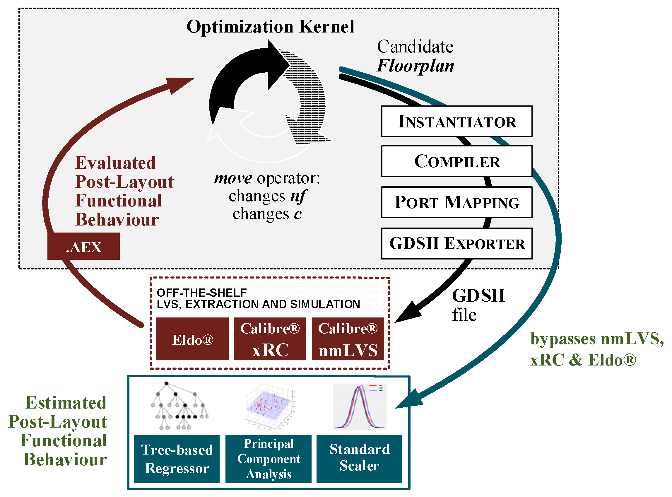

Table 3.
Summary of the M/DL Advances for analog Post-Layout Performance Prediction.
| Tool | Year | Key Specification | Tech. | Base Code |
|---|---|---|---|---|
| BagNet [76] | 2019 | ANN model acting as an oracle to select the most promising solution | 45nm | n/s |
| Liu [77] | 2020 | Net weights used as layout-related data and Bayesian optimization applied to optimize them | 40nm | C++ & Python |
| Chang [75] | 2023 | CNN used to classify floorplan solutions as “good”/“bad” | n/s | n/s |
| Wang [72] | 2024 | Transfer learning from pre- to post-layout within an evolutionary algorithm-based synthesis | 130-180nm | n/s |
| Li [73] | 2024 | Transfer learning from pre- to post-layout within RL-based synthesis | 130-180nm | Python |
| Ponderous [78] | 2024 | Post-placement performance regression pipeline using (x, y) placement coordinates | 65nm | Java & Python |
| Almeida [79] | 2025 | Convolutional VAEs and an ensemble of MLPs to estimate post-placement performance | 65nm | Python |
n/s – not specified.
4. Discussion
This paper conducted a review of the most recent analog IC automatic layout generation techniques powered by M/DL methods, covering placement, routing, and trends on post-layout performance estimation, providing an actual, complete and comprehensive guide for circuit designers and EDA developers. Regarding placement, two major research lines have been explored in the past few years, namely: (1) the usage of ANNs to pursue the knowledge mining path [28,29,30,31]. However, as the encoding of the circuits’ traits on the models’ input layer is still an open research question, graph-structured inputs have recently been exploited and are likely to continue an active research topic for the next years; and also, (2) the usage of RL-based approached to perform the cells’ moves the a floorplan [34,35,36,37,38]. SA has been historically the algorithm of choice for automatic analog IC placement, and the capabilities of RL on using an agent to choose the best action for a given environment state, instead of the random search nature of SA, is a promising contribution to automatic placement. Similarly to the ANN case, encoding the circuit characteristics is also a delicate topic, a condition where graph neural networks, that can accurately capture the hierarchical and topological features of circuit designs, and CNNs, will be determinant. A final note is left on generative artificial intelligence (AI) and large language models, whose application to analog IC placement is likely to launch, offering novel opportunities for enhancing layout automation, weather by providing new solutions not intuitive for circuit designers, detailed explanations of possible design choices (explainable AI), suggesting improvements based on historical data and/or patterns, and so on.
Concerning routing, it is possible to observe that most recent analog routing methods assisted by M/DL techniques are following two major trends: (1) dealing with analog layouts as images, and afterwards, using convolutional layers to identify uncovered patterns [58,59]; and also, (2) the use of RL to assist traditional routing methods in complex tasks that have been usually dealt with fixed heuristics, such as for net ordering, rip-up, reroute, and even, track-assignment [60,61,62,63]. Since these methodologies are still in the early stages of development, many ideas will likely be drawn from the established practices in digital IC routing, where M/DL is also leaving its mark. In this regard, several studies have proposed different approaches to predicting digital routing violations. In [81], various M/DL techniques were examined to predict design rule violations right after global routing, utilizing information such as wire density, connectivity, and pin proximity. In contrast, studies [82,83,84] focused on predicting routing short violations immediately after placement, disregarding global routing information and directly employing ANNs and CNNs. A concept related to violation prediction is design rule hotspot prediction, which identifies critical areas with multiple violations. While traditional hotspot prediction methods forecast hotspots after global routing, [85] used CNNs to predict hotspots with high accuracy right after placement. These techniques for predicting routing violations or detecting hotspots have been applied to improve the efficiency and performance of established routing processes. For instance, in [86], the routing problem is transformed into an RL-based collaborative system, where one agent detects violations while another agent is trained to perform the routing.
Finally, as layout-aware optimization of analog ICs became a reality in analog IC design, post-layout performance quantification has become fundamental. Three different research paths have been identified: (1) the direct transfer learning from pre to post-layout [70,71,72,73], however, the performance regression model becomes limited to its application to different layout styles as no layout implementation details are provided at the input layer of the transferred models, only sizing-related parameters; (2) classification-based approaches or oracles [74,75,76], that exploit ANNs and CNNs to identify the relative quality of a floorplan. Still, while these approaches may avoid several extractions and post-layout simulations when embedded into layout-aware sizing methodologies, they still do not quantify the post-layout performance, and thus, cannot guide an optimization process; and (3) the regression-based approaches [78,79,80], where the subjective classification is dropped and the exact post-layout performances are estimated. However, due to its complexity, only a few works have been reported in the literature so far exploiting VAEs and CNNs for this purpose, and therefore, post-layout performance estimation is likely to be vastly researched in the near future in the EDA community.
Funding
This research was funded by Fundação para a Ciência e a Tecnologia –Ministério da Ciência, Tecnologia e Ensino Superior (FCT/MCTES) through national funds and, when applicable co-founded European Union funds under the projects UIDB/50008/2020 (DOI identifier 10.54499/UIDB/50008/2020) and ACTON 2023.11981.PEX (DOI identifier 10.54499/2023.11981.PEX).
Conflicts of Interest
The funders had no role in the design of the study; in the collection, analyses, or interpretation of data; in the writing of the manuscript; or in the decision to publish the results.
Abbreviations
The following abbreviations are used in this manuscript:
| AI | Artificial Intelligence |
| ANN | Artificial Neural Network |
| B*-Tree | Binary Tree |
| BO | Bayesian Optimization |
| CAD | Computer-Aided Design |
| CNN | Convolutional Neural Network |
| DL | Deep Learning |
| EBL | Electron-Beam Lithography |
| EDA | Electronic Design Automation |
| GAN | Generative Adversarial Network |
| IC | Integrated Circuit |
| LDE | Layout-Dependent Effect |
| MDP | Markov Decision Process |
| M/DL | Machine and Deep Learning |
| MLP | Multi-Layer Perceptron |
| O-tree | Ordered Tree |
| PDK | Process Design Kit |
| R-GCN | Relational Graph Convolutional Neural Network |
| RL | Reinforcement Learning |
| SA | Simulated Annealing |
| SoC | System-on-a-Chip |
| SP | Sequence Pair |
| TCG | Transitive Closure Graph |
| VAE | Variational Autoencoder |
References
- Fayazi, M.; Colter, Z.; Afshari, E.; Dreslinski, R. Applications of Artificial Intelligence on the Modeling and Optimization for Analog and Mixed-Signal Circuits: A Review. IEEE TCAS-I 2021, 68, 6, 2418-2431. [CrossRef]
- Mina, R.; Jabbour, C.; Sakr, G. A Review of Machine Learning Techniques in Analog Integrated Circuit Design Automation. Electronics 2022, 11, 3, 435. [CrossRef]
- Maji, S.; Budak, A. F.; Poddar, S.; Pan, D. Z. Toward End-to-End Analog Design Automation with ML and Data-Driven Approaches (Invited Paper). 29th Asia and South Pacific Design Automation Conference (ASP-DAC), Incheon, Republic of Korea, Jan. 2024. [CrossRef]
- Wang, C.; Yang, F.; Zhu, K. AI-Enabled Layout Automation for Analog and RF IC: Current Status and Future Directions. IEEE International Symposium on Radio-Frequency Integration Technology (RFIT), Chengdu, China, Aug. 2024. [CrossRef]
- Graeb, H. (Editor). Analog Layout Synthesis: A Survey of Topological Approaches, Springer: New York, NY, 2011. [CrossRef]
- Lin, P.-H.; Chang, Y.-W.; Hung, C.-M. Recent research development and new challenges in analog layout synthesis. Asia and South Pacific Design Automation Conference (ASP-DAC), Macao, China, Jan. 2016. [CrossRef]
- Zhang, L.; Raut, R.; Jiang, Y.; Kleine, U. Placement Algorithm in Analog-Layout Designs. IEEE Trans. Comput. -Aided Des. Integr. Circuits Syst. 2006, 25, 1889–1903. [CrossRef]
- Martins, R.; Póvoa, R.; Lourenço, N.; Horta, N. Current-flow and current-density-aware multi-objective optimization of analog IC placement, Integration, the VLSI 2016, 55, 295-306. [CrossRef]
- Martins, R.; Lourenço, N.; Póvoa, R.; Horta, N. Shortening the Gap between Pre- and Post-Layout Analog IC Performance by Reducing the LDE-induced Variations with Multi-Objective Simulated Quantum Annealing. Engineering Applications of Artificial Intelligence 2021, 98, 104102. [CrossRef]
- Pang, Y.; Balasa, F.; Lampaert, K.; Cheng, C.-K. Block placement with symmetry constraints based on the o-tree nonslicing representation. Proceedings ACM/IEEE Design Automation Conference, Los Angeles, USA, June 2000.
- Balasa, F.; Maruvada, S.; Krishnamoorthy, K. Efficient solution space exploration based on segment trees in analog placement with symmetry constraints. IEEE/ACM International Conference on Computer-Aided Design (ICCAD), San Jose, USA, Nov. 2002. [CrossRef]
- Balasa, F.; Maruvada, S. C.; Krishnamoorthy, K. Using Red-Black Interval Trees in Device-Level Analog Placement with Symmetry Constraints. Proceedings of the Asian and South Pacific – Design Automation Conference (ASP-DAC), Kitakyushu, Japan, Jan. 2003. [CrossRef]
- Maruvada, S.; Berkman, A.; Krishnamoorthy, K.; Balasa, F. Deterministic skip lists in analog topological placement. Proc. 6th International Conference On ASIC (ASICON), Shanghai, China, Oct. 2005. [CrossRef]
- Zhang, L.; Shi, C.-J.; Jiang, Y. Symmetry-aware placement with transitive closure graphs for analog layout design. Proc. IEEE/ACM Asia South Pacific Des. Autom. Conf., Seoul, Korea, Mar. 2008. [CrossRef]
- Lin, J.-M.; Wu, G.-M.; Chang, Y.-W.; Chuang, J.-H. Placement with symmetry constraints for analog layout design using TCG-S. Proc. IEEE/ACM Asia South Pacific Des. Autom. Conf., Shanghai, China, Jan. 2005. [CrossRef]
- Lin, P.H.; Chang, Y.W.; Lin, S.C. Analog Placement Based on Symmetry-Island Formulation. IEEE Trans. Comput. Des. Integr. Circuits Syst. 2009, 28, 791–804. [CrossRef]
- Wu, I.P.; Ou, H.C.; Chang, Y.W. QB-Trees: Towards an Optimal Topological Representation and Its Applications to Analog Layout Designs. In Proceedings of the Design Automation Conference, Austin, TX, USA, 5–9 June 2016. [CrossRef]
- Balasa, F.; Lampaert, K. Symmetry within the sequence-pair representation in the context of placement for analog design. IEEE Transactions on Computer-Aided Design of Integrated Circuits and Systems (TCAD) 2000, 19, 7, 721-731. [CrossRef]
- Koda, S.; Kodama, C.; Fujiyoshi, K. Linear programming-based cell placement with symmetry constraints for analog IC layout. IEEE Transactions on Computer-Aided Design Integrated Circuits and Systems 2007, 26, 4, 659–668. [CrossRef]
- Tam, Y.-C.; Young, Y.; Chu, C. Analog placement with symmetry and other placement constraints. in Proc. IEEE/ACM Int. Conf. Comput.-Aided Des., San Jose, USA, Nov. 2006. [CrossRef]
- Krishnamoorthy, K.; Maruvada, S.; Balasa, F. Topological placement with multiple symmetry groups of devices for analog layout design. IEEE International Symposium on Circuits and Systems (ISCAS), New Orleans, USA, May 2007. [CrossRef]
- Patyal, A.; Pan, P.-C.; Asha, K.A.; Chen, H.-M.; Chi, H.-Y.; Liu, C.-N. Analog placement with current flow and symmetry constraints using pcp-sp. In Proceedings of the ACM/ESDA/IEEE Design Automation Conference (DAC), San Francisco, CA, USA, 24–28 June 2018. [CrossRef]
- Jangkrajarng, N.; Bhattacharya, S.; Hartono, R.; Shi, R. IPRAIL—Intellectual property reuse-based analog IC layout automation. Integr. VSLI 2003, 36, 237–262. [CrossRef]
- Pan, P.C.; Chin, C.Y.; Chen, H.M.; Chen, T.C.; Lee, C.C.; Lin, J.C. A Fast Prototyping Framework for Analog Layout Migration with Planar Preservation. IEEE Trans. Comput. Des. Integr. Circuits Syst. 2015, 34, 1373–1386. [CrossRef]
- Martins, R.; Lourenço, N.; Horta, N. LAYGEN II: Automatic analog ICs layout generator based on a template approach. Proceedings of the 14th annual conference on Genetic and evolutionary, Philadelphia, USA, July 2012. [CrossRef]
- Wu, P.H.; Lin, M.P.H.; Chen, T.C.; Yeh, C.F.; Li, X.; Ho, T.Y. A Novel Analog Physical Synthesis Methodology Integrating Existent Design Expertise. IEEE Trans. Comput. Des. Integr. Circuits Syst. 2015, 34, 199–212. [CrossRef]
- He, R.; Zhang, L. Artificial neural network application in analog layout placement design. Canadian Conference on Electrical and Computer Engineering, St. John’s, Canada, June 2009. [CrossRef]
- Guerra, D.; Canelas, A.; Póvoa, R.; Horta, N.; Lourenço, N.; Martins, R. Artificial Neural Networks as an Alternative for Automatic Analog IC Placement. SMACD 2019 - 16th International Conference on Synthesis, Modeling, Analysis and Simulation Methods and Applications to Circuit Design, Lausanne, Switzerland, July 2019. [CrossRef]
- Gusmao, A.; Passos, F.; Povoa, R.; Horta, N.; Lourenco, N.; Martins, R. Semi-Supervised Artificial Neural Networks towards Analog IC Placement Recommender. 2020 IEEE International Symposium on Circuits and Systems (ISCAS), Seville, Spain, October 2020. [CrossRef]
- Gusmão, A.; Póvoa, R.; Horta, N.; Lourenço, N.; Martins, R. DeepPlacer: A Custom Integrated OpAmp Placement Tool Using Deep Models. Appl. Soft Comput. 2022, 115, 108188. [CrossRef]
- Gusmão, A.; Horta, N.; Lourenço, N.; Martins, R. Scalable and Order Invariant Analog Integrated Circuit Placement with Attention-Based Graph-to-Sequence Deep Models. Expert Syst. Appl. 2022, 207, 117954. [CrossRef]
- Xu, B.; Lin, Y.; Tang, X.; Li, S.; Shen, L.; Sun, N.; Pan, D. Z. WellGAN: Generative-adversarial-network-guided well generation for analog/mixed-signal circuit layout. 2019 56th ACM/IEEE Design Automation Conference (DAC), Las Vegas, USA, June 2019.
- Zhu, K.; Chen, H.; Liu, M.; Tang, X.; Shi, W.; Sun, N.; Pan, D. Z. Generative-adversarial-network-guided well-aware placement for analog circuits. in 27th Asia and South Pacific Design Automation Conference (ASP-DAC), Taipei, Taiwan, Jan. 2022. [CrossRef]
- Ahmadi, M.; Zhang, L. Analog Layout Placement for FinFET Technology Using Reinforcement Learning. IEEE International Symposium on Circuits and Systems (ISCAS), Daegu, Korea, May 2021. [CrossRef]
- Basso, D.; Bortolussi, L.; Videnovic-Misic, M.; Habal, H. Fast ML Driven Analog Circuit Layout using Reinforcement Learning and Steiner Trees. 20th International Conference on Synthesis, Modeling, Analysis and Simulation Methods and Applications to Circuit Design (SMACD), Volos, Greece, 2024. [CrossRef]
- Basso, D.; Bortolussi, L.; Videnovic-Misic, M.; Habal, H. Effective Analog ICs Floorplanning with Relational Graph Neural Networks and Reinforcement Learning. Design, Automation and Test in Europe Conference, Lyon, France, March 2025.
- Hajijafari, M.; Ahmadi, M.; Zhao, Z.; Zhang, L. Fogging-effect-aware mixed-signal IC placement with reinforcement learning. Proc. IEEE International Symposium on Circuits and Systems (ISCAS), Austin, USA, May 2022. [CrossRef]
- Sadrafshari, M.; Dobre, O.; Zhang, L. Reinforcement-Learning-Based Foggy-Aware Optimal Placement Method for Analog and Mixed-Signal Circuits. IEEE International Symposium on Circuits and Systems (ISCAS), Singapore, May 2024. [CrossRef]
- Martins, R.; Lourenço, N. Analog Integrated Circuit Routing Techniques: An Extensive Review. IEEE Access 2023, 11, 35965-35983. [CrossRef]
- Owen, B.; Duncan, R.; Jantzi, S.; Ouslis, C.; Rezania, S.; Martin, K. BALLISTIC: An analog layout language. Proceedings of the IEEE 1995 Custom Integrated Circuits Conference, Santa Clara, CA, USA, Aug. 1995. [CrossRef]
- Sampath, H.; Vemuri, R. MSL: A High-Level Language for Parameterized Analog and Mixed-Signal Layout Generators. Proc. Of IFIP International Conf. on VLSI, Jan. 2003.
- E. Chang, et. al. Bag2: A process-portable framework for generator-based ams circuit design. IEEE Custom Integrated Circuits Conference (CICC), San Diego, USA, April 2018. [CrossRef]
- Han, J.; Bae, W.; Chang, E.; Wang, Z.; Nikolić, B.; Alon, E. LAYGO: A Template-and-Grid-Based Layout Generation Engine for Advanced CMOS Technologies. IEEE Transactions on Circuits and Systems I: Regular Papers (TCAS-I) 2021, 68, 3, 1012-1022. [CrossRef]
- Bhattacharya, S.; Jangkrajarng, N.; Hartono, R.; Shi, R. Correct by-construction layout-centric retargeting of large analog designs. Proceedings 41st Design Automation Conference, San Diego, USA, July 2004.
- Lourenço, N.; Vianello, M.; Guilherme, J.; Horta, N. LAYGEN - Automatic Layout Generation of Analog ICs from Hierarchical Template Descriptions. Ph.D. Research in Microelectronics and Elec., Otranto, Italy, June 2006. [CrossRef]
- Unutulmaz, A.; Dundar, G.; Fernandez, F. A template router. European Conference on Circuit Theory and Design (ECCTD), Sweden, Aug. 2011. [CrossRef]
- Rijmenants, J.; Litsios, J.; Schwarz, T.; Degrauwe, M. ILAC: An automated layout tool for analog CMOS circuits. IEEE Journal of Solid-State Circuits 1989, 24, 12, 417–425. [CrossRef]
- Zhang, L.; Kleine, U.; Jiang, Y. An Automated Design Tool for Analog Layouts. IEEE Transactions on Very Large Scale Integration (VLSI) Systems 2006, 14, 8, 881–894. [CrossRef]
- Yilmaz, Y.; Dundar, G. Analog Layout Generator for CMOS Circuits. IEEE Transactions on Computer-Aided Design of Integrated Circuits and Systems 2009, 28, 1, 32–45. [CrossRef]
- Malavasi, E.; Sangiovanni-Vincentelli, A. Area routing for analog layout. IEEE Transactions on Computer-Aided Design of Integrated Circuits and Systems 1993, 12, 8, 1186-1197. [CrossRef]
- Rijmenants, J.; Litsios, J.; Schwarz, T.; Degrauwe, M. ILAC: An automated layout tool for analog CMOS circuits. IEEE Journal of Solid-State Circuits 1989, 24, 12, 417–425. [CrossRef]
- Cohn, J.; Garrod, J.; Rutenbar, R.; Carley, L. KOAN/ANAGRAM II: New Tools for Device-Level Analog Placement and Routing. IEEE Journal of Solid-State Circuits 1991, 26, 3, 330-342. [CrossRef]
- Chen H. et al. MAGICAL: An Open- Source Fully Automated Analog IC Layout System from Netlist to GDSII. IEEE Design & Test 2021, 38, 2, 19-29. [CrossRef]
- Ou, H.-C.; Chien, H.-C.; Chang, Y.-W. Non-uniform multilevel analog routing with matching constraints. IEEE Transactions on Computer-Aided Design of Integrated Circuits and Systems 2014, 33, 12, 1942–1954. [CrossRef]
- Martins, R.; Lourenco, N.; Horta, N. Routing analog ICs using a multiobjective multi-constraint evolutionary approach. Analog Integrated Circuits and Signal Processing 2014, 78, 1, 123-135. [CrossRef]
- Martins, R.; Lourenço, N.; Canelas, A.; Horta, N. Electromigration-aware analog Router with multilayer multi-port terminal structures. Integration, the VLSI 2014, 47, 4, 532-547. [CrossRef]
- Martins, R.; Lourenço, N.; Canelas, A.; Horta, N. Electromigration-aware and IR-drop avoidance routing in analog multiport terminal structures. Design, Automation & Test in Europe Conference & Exhibition (DATE), Dresden, Germany, March 2014. [CrossRef]
- Zhu, K. et al. Geniusroute: a new analog routing paradigm using generative neural network guidance. IEEE/ACM International Conference on Computer-Aided Design (ICCAD), Westminster, USA, Nov. 2019. [CrossRef]
- Peneda, D.; Azevedo, F.; Lourenço, N.; Horta, N.; Martins, R. Effective Routing Probability Maps via Convolutional Neural Networks for Analog IC Layout Automation. 20th International Conference on Synthesis, Modeling, Analysis and Simulation Methods and Applications to Circuit Design (SMACD), Volos, Greece, July 2024. [CrossRef]
- Liao, H.; et al. Attention Routing: track assignment detailed routing using attention-based reinforcement learning. arXiv:2004.09473, 2020.
- Liao, H.; Dong, Q.; Qi, W.; Fallon, E.; Kara, L. Track-Assignment Detailed Routing Using Attention based Policy Model With Supervision. ACM/IEEE 2nd Workshop on Machine Learning for CAD (MLCAD), Reykjavik, Iceland, Nov. 2020. [CrossRef]
- Chen, H.; Hsu, K.-C.; Turner, W. J.; Wei, P.-H.; Zhu, K.; Pan, D. Z.; Ren, H. Reinforcement learning guided detailed routing for custom circuits. Proceedings of the International Symposium on Physical Design, New York, USA, March 2023. [CrossRef]
- Yeh, Y.-H. et al. DPRoute: Deep Learning Framework for Package Routing. 28th Asia and South Pacific Design Automation Conference, Tokyo, Japan, Jan. 2023.
- Xu, P.; Li, J.; Ho, T.-Y.; Yu, B.; Zhu, K. Performance-Driven Analog Layout Automation: Current Status and Future Directions (Invited Paper). 29th Asia and South Pacific Design Automation Conference (ASP-DAC), Incheon, Korea, Republic of, 2024. https://10.1109/ASP-DAC58780.2024.10473859.
- Choudhury, U.; Sangiovanni-Vincentelli, A. Automatic generation of parasitic constraints for performance-constrained physical design of analog circuits. IEEE Transactions on Computer-Aided Design of Integrated Circuits and Systems 1993, 12, 2, 208-224. [CrossRef]
- Gielen, G.; Lampaert, K. Direct Performance-Driven Placement of Mismatch-sensitive Analog Circuits. 32nd Design Automation Conference, San Francisco, USA, June 1995. [CrossRef]
- Lampaert, K.; Gielen, G.; Sansen, W. A performance-driven placement tool for analog integrated circuits. IEEE Journal of Solid-State Circuits 1995, 30, 7, 773–780. [CrossRef]
- Li, Y.; Lin. Y.; Madhusudan, M.; Sharma, A.; Xu, W.; Sapatnekar, S.; Harjani, R.; Hu, J. Exploring a Machine Learning Approach to Performance Driven Analog IC Placement. IEEE Computer Society Annual Symposium on VLSI (ISVLSI), Limassol, Cyprus, July 2020. [CrossRef]
- Pan, P.-C.; Huang, H.-W.; Huang, C.-C.; Patyal, A.; Chen, H.-M.; Yang, T.-Y. On Closing the Gap Between Pre-simulation and Post-simulation Results in Nanometer Analog Layouts. 15th International Conference on Synthesis, Modeling, Analysis and Simulation Methods and Applications to Circuit Design (SMACD), Prague, Czech Republic, July 2018. [CrossRef]
- Wang, Z.; et al. Building Post-layout Performance Model of Analog/RF Circuits by Fine-tuning Technique. 23rd International Symposium on Quality Electronic Design (ISQED), Santa Clara, USA, June 2022. [CrossRef]
- Wang, Z.; et al. Building a post-layout simulation performance model with global mapping model fusion technique," in Tsinghua Science and Technology 2022, 27, 3, 512-525. [CrossRef]
- Wang, Z.; Ye, Z.; Zhou, J.; Liu, X.; Wang, Y. A Two-step Fine-tuning Assisted Layout Sizing Scheme for Analog/RF Circuits. IEEE International Symposium on Circuits and Systems (ISCAS), Singapore, Singapore, May 2024. [CrossRef]
- Li, Z.; Carusone, A. An Open-Source AMS Circuit Optimization Framework Based on Reinforcement Learning—From Specifications to Layouts. IEEE Access 2024, 12, 150032-150045. [CrossRef]
- Liu, M.; Zhu, K.; Gu, J.; Shen, L.; Tang, X.; Sun, N.; Pan, Z. Towards Decrypting the Art of Analog Layout: Placement Quality Prediction via Transfer Learning. Design Automation and Test in Europe Conference, Grenoble, France, March 2020. [CrossRef]
- Chang, C.-C.; Pan, J.; Xie, Z.; Li, Y.; Lin, Y.; Hu, J.; Chen, Y. Fully Automated Machine Learning Model Development for Analog Placement Quality Prediction. Asia and South Pacific Design Automation Conference (ASP-DAC), Tokyo, Japan, Jan. 2023.
- K. Hakhamaneshi, K.; Werblun, N.; Abbeel, P.; Stojanovic, V. BagNet: Berkeley Analog Generator with Layout Optimizer Boosted with Deep Neural Networks. International Conference on Computer-Aided Design, Westminster, USA, Nov. 2019. [CrossRef]
- Liu, M.; Zhu, K.; Tang, X.; Xu, B.; Shi, W.; Sun, N.; Pan, D. Z. Closing the design loop: Bayesian optimization assisted hierarchical analog layout synthesis. 57th ACM/IEEE Design Automation Conference (DAC), San Francisco, USA, July 2020. [CrossRef]
- Martins, R. Closing the Gap Between Electrical and Physical Design Steps with an Analog IC Placement Optimizer Enhanced with Machine-Learning-Based Post-Layout Performance Regressors. Electronics 2024, 13, 22, 4360.
- Almeida, C.; Oliveira, M.; Martins, R. On the Exploration of Convolutional Variational Autoencoders for Analog Integrated Circuit Post-Placement Performance Regression. International Conference on Synthesis, Modeling, Analysis and Simulation Methods and Applications to Circuit Design (SMACD), Istanbul, Turkey, July 2025. (in press).
- Golzan, M.; Nasiri, H.; Ngatched, T.; Popuri, K.; Zhang, L. Advanced Performance Estimation of Analog Layouts Using Convolutional Neural Networks. IEEE 20th International Conference on Intelligent Computer Communication and Processing (ICCP), Cluj-Napoca, Romania, Oct. 2024. [CrossRef]
- Chan, W.-T.; Ho, P.-H-; Kahng, A.; Saxena, P. Routability optimization for industrial designs at sub-14nm process nodes using machine learning. Proceedings of the International Symposium on Physical Design, New York, USA, March. 2017.
- Tabrizi, A. et al. A machine learning framework to identify detailed routing short violations from a placed netlist. 55th ACM/ESDA/IEEE Design Automation Conference (DAC), San Francisco, USA, June 2018. [CrossRef]
- Yu, T.-C. et al. Pin accessibility prediction and optimization with deep learning-based pin pattern recognition. 56th ACM/IEEE Design Automation Conference, Las Vegas, USA, June 2019.
- Yu, T.C. et al. Lookahead placement optimization with cell library-based pin accessibility prediction via active learning. Proceedings of the International Symposium on Physical Design, New York, USA, Sept. 2020. [CrossRef]
- Liang, R. et al. DRC hotspot prediction at sub-10nm process nodes using customized convolutional network. Proceedings of the International Symposium on Physical Design, New York, USA, 2020. [CrossRef]
- Gandhi, U.; Bustany, I.; Swartz, W.; Behjat, L. A reinforcement learning-based framework for solving physical design routing problem in the absence of large test sets. ACM/IEEE Workshop on Machine Learning for CAD, Canmore, Canada, Sept. 2019. [CrossRef]
Figure 1.
Traditional analog IC design flow, where the real layout-impact is only known after post-layout simulation.
Figure 1.
Traditional analog IC design flow, where the real layout-impact is only known after post-layout simulation.
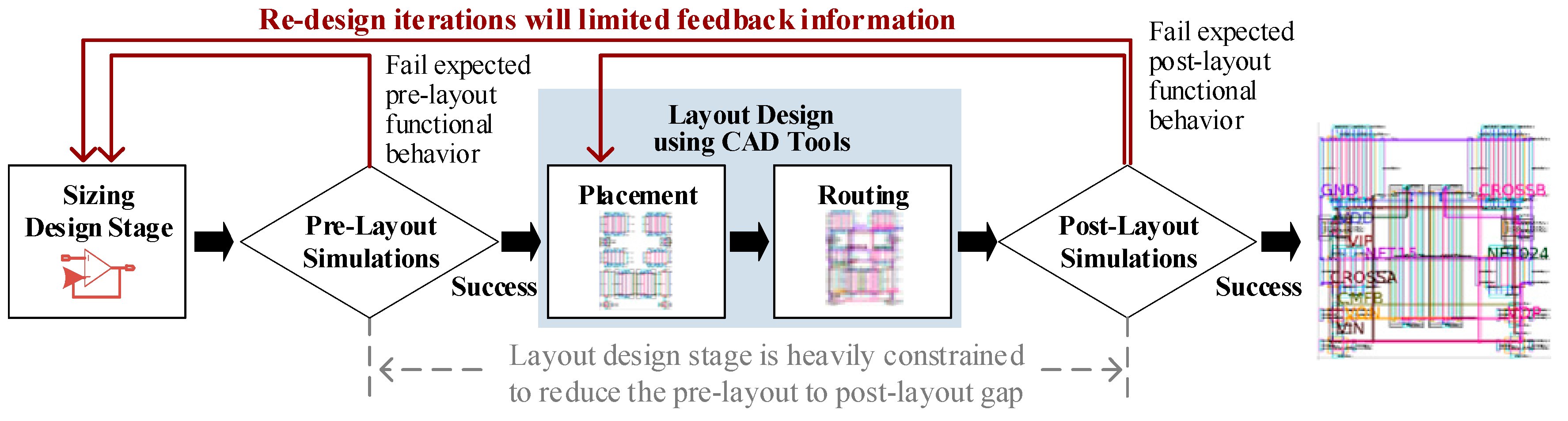
Figure 2.
ANN used to pursue knowledge mining on analog IC placement (adapted from [28]).
Figure 2.
ANN used to pursue knowledge mining on analog IC placement (adapted from [28]).
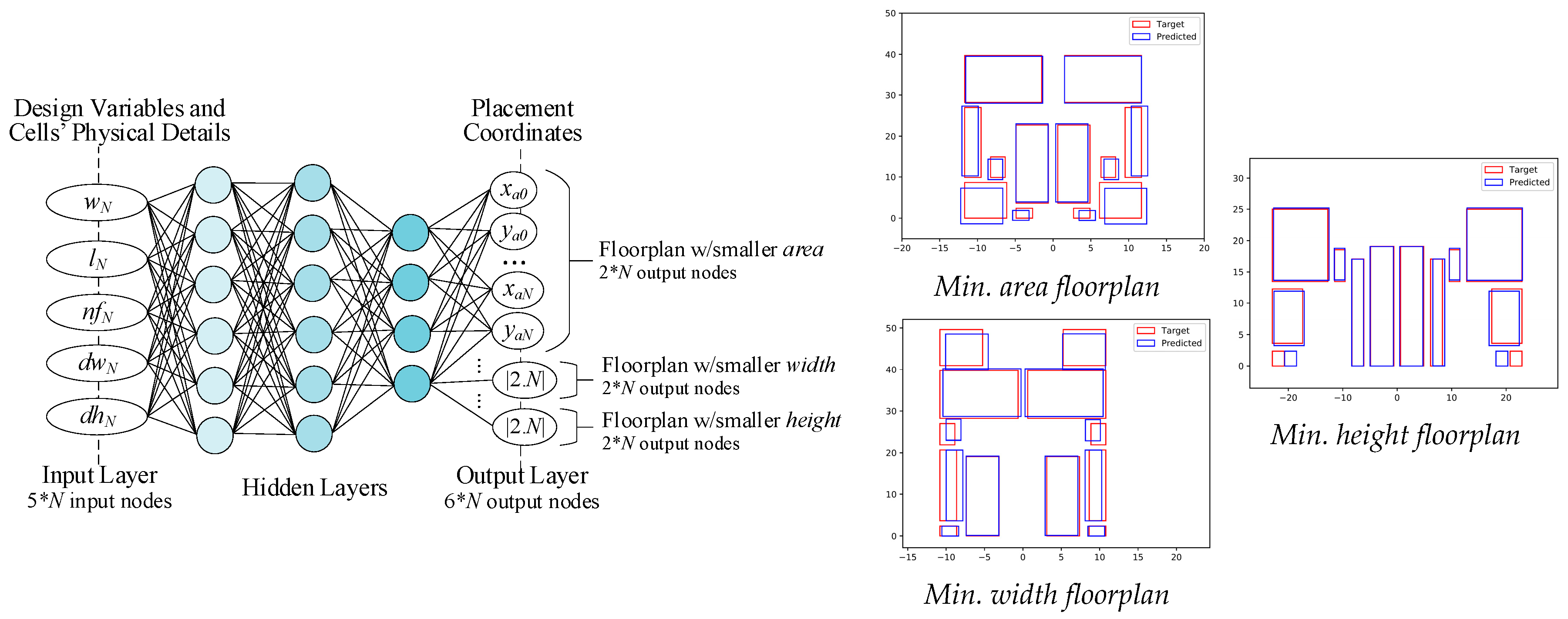
Figure 3.
Embedding placement topological constraints at an ANN’s input layer through directed graphs (adapted from [30]).
Figure 3.
Embedding placement topological constraints at an ANN’s input layer through directed graphs (adapted from [30]).
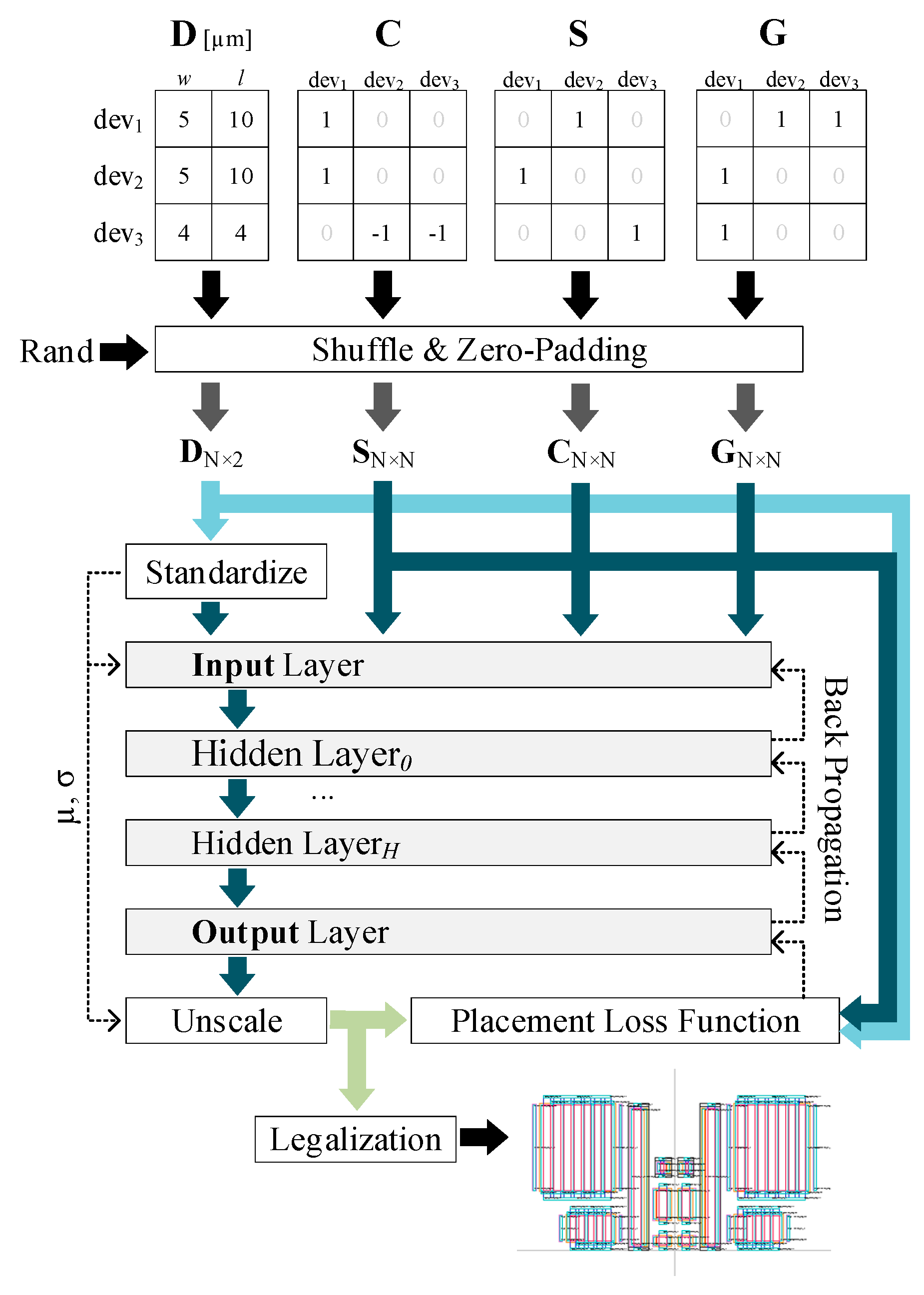
Figure 4.
CNN-based approach to solve analog IC single-net routing problems (adapted from [59]).
Figure 4.
CNN-based approach to solve analog IC single-net routing problems (adapted from [59]).
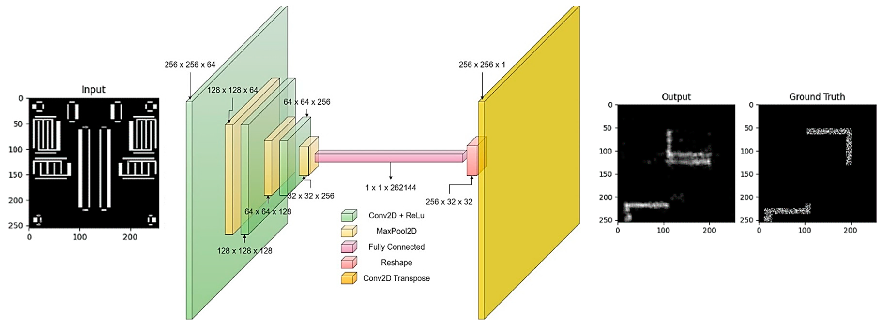
Table 1.
Summary of the M/DL Advances for Analog IC Placement.
| Tool | Year | Key Specification | Tech. | Base Code |
|---|---|---|---|---|
| He [27] | 2009 | ANN’s neurons used a discrete space where devices can be placed | n/d | Java |
| Guerra [28] | 2019 | ANN used for knowledge mining of legacy floorplans | 130nm | Python |
| Ahmadi [34] | 2021 | RL approach for placement on advanced FinFET technologies | 18nm | Python |
| WellGAN [33] | 2022 | Exploration of GANs for well-aware guided placement | 40nm | C++ & Python |
| DeepPlacer [30] | 2022 | ANN evaluated by a topological constraint satisfaction loss function | 65-350nm | Python |
| Graph2Seq [31] | 2022 | Graph-structured input in a scalable attention-based encoder-decoder model | 65-350nm | Python |
| Basso [35] | 2024 | RL performs the moves of the underlying SP topological representation | n/s | Python |
| Sadrafshari [38] | 2024 | RL performs the moves of the underlying B*-tree representation | 10nm | Python |
| Basso [36] | 2025 | R-GCN used as an encoder of the circuit, device and geometric constraints | n/s | Python |
n/s – not specified.
Table 2.
Summary of the M/DL Advances for Analog IC Routing.
| Tool | Year | Key Specification | Tech. | Base Code |
|---|---|---|---|---|
| GeniusRoute [57] | 2019 | Routing probability maps generated by a VAE, and used to guide a path-finding algorithm | 40nm | Python & C++ |
| REINFORCE [60,61] | 2020 | RL that solves the track-assignment problem | 16nm | Python |
| DPRoute [63] | 2023 | RL that solves the net ordering problem | n/s | Python |
| Chen [62] | 2023 | RL-guided rip-up and rerouting scheme | FinFET | Python & C++ |
| Peneda [59] | 2024 | Routing probability maps generated by a CNN, trained on large amounts of synthetically generated data | 65nm | Python |
n/s – not specified.
Disclaimer/Publisher’s Note: The statements, opinions and data contained in all publications are solely those of the individual author(s) and contributor(s) and not of MDPI and/or the editor(s). MDPI and/or the editor(s) disclaim responsibility for any injury to people or property resulting from any ideas, methods, instructions or products referred to in the content. |
© 2025 by the authors. Licensee MDPI, Basel, Switzerland. This article is an open access article distributed under the terms and conditions of the Creative Commons Attribution (CC BY) license (http://creativecommons.org/licenses/by/4.0/).
Copyright: This open access article is published under a Creative Commons CC BY 4.0 license, which permit the free download, distribution, and reuse, provided that the author and preprint are cited in any reuse.


