Submitted:
15 March 2025
Posted:
17 March 2025
You are already at the latest version
Abstract
Thin films of bismuth sulfide (Bi2S3) on fluorine doped tin oxide (FTO) coated glass slides were successfully formed by the chemical bath deposition (CBD) method. In this work, a new sulfur precursor L-cysteine was used instead of the typical sulfur precursors such as urea, thiosulfate or thioacetamide used for the formation of Bi2S3 films by the CBD method. The synthesized Bi2S3 thin film on FTO substrate was subjected to characterization techniques including X-ray diffraction (XRD), scanning electron microscopy (SEM), energy dispersive X-ray spectroscopy (EDS) and UV–Visible spectroscopy analysis. X-ray diffraction analysis showed that initially, Bi2S3 films of amorphous structure with elemental sulfur impurities were formed on the FTO surface. During the annealing of the samples, amorphous Bi2S3 was transformed into its crystalline phase with an average crystallite size of about 22.06 nm. EDS studies confirmed that some of the sulfur not bound to bismuth during annealing was removed from the Bi2S3 films. The influence of the morphology of Bi2S3 films on their optical properties was confirmed by studies in the UV-visible range.
Keywords:
Bismuth sulfide film
; CBD
; XRD
; SEM
1. Introduction
Accelerating climate change, rapidly growing populations, and the resulting pollution are forcing a shift away from fossil fuels to clean and sustainable energy sources. And solar energy is one of them. It is imperative to develop innovative, efficient, and resource-saving solar energy technologies that have a lower impact on the environment. Non-toxic, earth abundant, and stable, bismuth is an ideal alternative to poisonous lead, cadmium, or mercury in environmentally friendly solar panels. Furthermore, non-toxic bismuth sulfide (Bi2S3) thin films are of great interest as a component of solar cells due to their high efficiency of converting incoming photons into electrons. Bi2S3 is classified as an n-type semiconductor with a direct optical band gap between 1.3 and 2.2 eV and a high absorption coefficient of 105 cm–1 [1]. According to the Beer-Lambert law, a 200 nm thick Bi2S3 film can absorb 95% of the incident radiation. Due to the optical and electro-optical properties of Bi2S3 films, they are widely used in optoelectronic and thermoelectric devices, such as such as photo-catalysts[2], hydrogen storage [3], optical-detection for infrared [4] and UV light [5], etc. Furthermore, Bi2S3 thin films can be used as efficient anode materials for lithium-ion batteries [6], as thermoelectric hydrogen [7] gas sensors [8]or memristors [9], and even for cancer diagnostics [10,11]. Bi2S3 thin films can be grown using physical processes, including spray pyrolysis [12], pulsed laser deposition [13], chemical vapor deposition [14], thermal evaporation [15], and etc. However, the above methods for forming Bi2S3 thin films have various disadvantages, such as requiring complex equipment, high temperature, ultrahigh vacuum environment, and high cost. While wet methods such as chemical bath deposition (CBD) and successive ion layer adsorption and reaction (SILAR) of chalcogenide films is very promising due to low deposition cost, ease of equipment use and large surface area deposition capability. During the formation of films by the CBD method, the substrate, all cationic and anionic precursors are present in the same reaction bath. This allows for the production of films in one step and the simultaneous control of film deposition. Therefore, in this work, the chemical bath deposition (CBD) method was used to form thin films of Bi2S3. The optoelectronic properties of films depend on their morphology, crystallinity, and the shape and size of the nanoparticles they contain. A wide range of morphologies of Bi2S3 nanostructures is also known, such as stars, balls, belts, ribbons, flowers, snowflakes, tubes, rods, and wires [16]. The microstructure of sulfide films is significantly affected by sulfur sources [17,18] and the metal-to-sulfur ratio [18]. For the deposition of Bi2S3 thin films by the CBD method, thioacetamide, thiourea, and thiosulfate [19] are usually used as sulfur-releasing precursors. L-cysteine is a promising sulfur precursor, but it is significantly less studied than the precursors listed above. Bi2S3 nanoparticles of various shapes and sizes and their heterostructures were synthesized using L-cysteine as a sulfur precursor using two-step hydrothermal [20,21] or solvothermal [22] methods. Meanwhile, Bi2S3 layers were formed using L-cysteine by the electrodeposition method [23]. However, detailed studies on the preparation of Bi2S3 thin film by the inexpensive and technologically simple CBD method have not yet been published. Thus, the main objective of this study was to form Bi2S3 films by wet chemistry methods such as CBD, and to study in detail the crystallinity, morphological, and optical properties of these films.
2. Materials and Methods
2.1. Materials
All materials were 99.99% pure, obtained from Sigma Aldrich and used as received. For the synthesis of Bi2S3 thin films, bismuth nitrate pentahydrate Bi(NO3)3 × 5H2O and L-cysteine were used as the precursors, while Ethylenediaminetetraacetic acid disodium salt (EDTA-Na2) was used as a chelating agent. The fixanals of 0.1 mol/L nitric acid (Fluka) and 0.025 mol/L EDTA-Na2 disodium salt solution (Chem-Lab) were also used to prepare solutions. Fluorine doped tin oxide (FTO) coated glass slides (by Merck) were used as substrates for the deposition of Bi2S3 films.
2.2. Formation of Bi2S3 Films
Pre-structured FTO slides (300 mm × 300 mm × 2.2 mm, surface resistivity ~7 Ω/sq) were cleaned with soapy water, then with acetone and distilled water in an ultrasonic bath each step for 10 min, and finally dried in a desiccator over silica gel granules. The 0.1 mol/L bismuth precursor solution was prepared by dissolving 48.5 g Bi(NO3)3 × 5H2O in a minimum volume of 1 M nitric acid with magnetic stirring at 300 rpm until dissolved, and then diluted with distilled water to 1 liter. The solution for forming Bi2S3 films was prepared by mixing 0.1 mol/L Bi(NO3)3 and 0.025 mol/L EDTA-Na2 solutions, then raising the temperature of the resulting solution to 80 °C and adding L-cysteine powder while stirring. After 5 min, FTO was immersed in this solution and kept for 8 h. When L-cysteine powder is added to the clear, colorless bismuth nitrate solution prepared for the experiment, the solution turns light yellow. This solution remains clear and light yellow throughout the experiment. Meanwhile, a black thin film of Bi2S3 gradually forms on the surface of the FTO slide. The composition of the solutions used is tabled in Table 1. At the end of the experiment, the FTO slide samples were removed from the vessel, washed with distilled water for 20 s, dried in a desiccator for 24 h, and then used in further studies. FTO slides with Bi2S3 films were annealed at 300 °C for 20 min. The preparation of Bi2S3 films on FTO slides by the CBD method are shown in Figure 1.
2.3. Characterization Methods of Bi2S3 Films
X-ray structural analysis of Bi2S3 films formed on FTO plates was performed using a D8 Advance diffractometer (Bruker AXS, Karlsruhe, Germany) with a high-speed one-dimensional Bruker LynxEye detector for recording diffraction patterns. The sizes of the Bi2S3 crystallites were calculated using the Scherrer formula based on the X-ray diffraction data along a given crystallographic plane:
where, D is the average crystallite size, λ – X-ray wavelength (1.54178Å), k – the shape factor (k=0.9), θ = Bragg’s angle, and β is full-width at half-maximum (FWHM) of the peak. The phase composition of the formed films was determined using the Crystallographica Search-Match v. 2.1 and ConvX v.1.0 software. The surface structure and morphology of Bi2S3 thin films formed on the FTO plates were studied by scanning electron microscopy (SEM) using a Hitachi S–3400N scanning electron microscope (Chiyoda, Tokyo, Japan, magnification 1000× and 10000×, scale 50 μm and 5 μm). The elemental composition of these films was determined by energy-dispersive X-ray spectroscopy (EDS) using an analyzer (JEOL-JSM 6360 A). UV–Vis spectra were recorded at room temperature on a PerkinElmer Lambda 35 UV/VIS Spectrometer (Waltham, Massachusetts, United States). To compensate for the absorption of the PP strip band in the range of 200–900 nm, the Diffuse Reflectance Sphere Labsphere RSA-PE-20 was used.
3. Results and Discussion
3.1. XRD Characterization
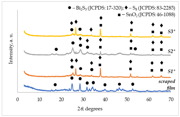
The structural characterization of the obtained Bi2S3 films on FTO slides was carried out using X-ray diffraction. XRD data of Bi2S3 films were interpreted in detail using combinations of data available in the literature [24,25] and JCPDS reference templates. The results of X-ray diffraction analysis are shown in Figure 2 and Figure 3, and the corresponding peak values are tabled in Table 2. Although the surface of samples 1–3 was obviously changed after the formation of Bi2S3 films on them, the XRD patterns presented in Figure 2 do not show any peaks attributed to any bismuth sulfide phase. Here it can also be seen that the formed films contain a single-crystal phase of orthorhombic sulfur S8 (JCPDS: 83-2285). It is also important to note that six of the seven sulfur peaks, including the three most intense ones at 2θ = 26.66, 33.87 and 51.69o, overlap with FTO peaks. Therefore, it is likely that the film formed on the FTO surface consists of the amorphous phase Bi2S3 and the crystalline phase of sulfur S8. The effect of annealing on the morphology, microstructure, crystallite size, phase composition and optical properties of metal chalcogenide films on the surface of various carriers has been confirmed in our studies [26,27]. Therefore, in this work, we expected that amorphous Bi2S3 would transform into a crystalline form during annealing. The X-ray diffraction patterns 1*–3* shown in Figure 3 confirmed that the films on the FTO slides formed a crystalline phase of orthorhombic bismuth sulfide (JCPDS: 17-320) during the annealing process, with five peaks assigned to it at 2θ = 17.69, 25.20, 28.75, 31.89 and 52.56°. Therefore, from the peaks of the diffraction patterns shown in Figure 2 and Figure 3 and the data in Table 2, it can be said that the peaks of Bi2S3, elemental sulfur S8 and SnO2 are in very similar positions and most of them overlap each other. For example, the most intense peaks of the diffraction patterns such as 2θ = 26.66, 33.87, 37.91, 51.69, 61.74 and 65.72° can be attributed to SnO2 (JCPDS: 46–1088), which is located on the surface of the FTO glass slide. The most intense peaks of the crystalline phase of Bi2S3 are observed in the X-ray diffraction patterns of sample S2*, which indicates the formation of a layer with the highest concentration of Bi2S3 on it. To finally verify that the film on the FTO surface after annealing consists only of the crystalline phase Bi2S3, we scraped it off the surface of the glass slide and recorded its diffraction pattern. This diffraction pattern is presented in Figure 3, which shows eight peaks of different intensities at 2θ = 17.43, 24.98, 28.67, 31.85, 35.51, 39.92, 46.42 and 52.52o attributed to the orthorhombic phase of Bi2S3 (JCPDS: 17-320). Also using the Scherrer formula, the crystallite size of the scraped film was estimated to be 22.06 nm. Thus, the obtained X-ray diffraction data indicate that after annealing, the orthorhombic phase Bi2S3 (JCPDS: 17-320) dominates in the film on the FTO slide of sample S2*.
3.2. SEM/EDX Characterization
The surface morphology and elemental composition of the Bi2S3 thin films formed on the surface of the FTO slides were evaluated using scanning electron and energy dispersive X-ray spectroscopy. SEM images of these films before and after annealing as well as the FTO slide without the film at different magnifications are shown in Figure 4. By comparing the SEM image of the FTO slide and samples S1–S3, it can be clearly stated that films were formed on the surface of the glass substrates. It is important to note that the SEM images of samples S1–S3 show typical amorphous layers with irregularly shaped particles and aggregates of different sizes, unevenly distributed over the entire surface area. The insets show that the particle and aggregate sizes vary widely from 10 nm to 5 µm. The surface morphology of Bi2S3 films on FTO slides changed dramatically after their annealing. As can be seen from the SEM images of samples S1* – S3* in Figure 3, the previously typical amorphous films were transformed into crystalline ones. The insets show that after annealing, uniform, densely packed films containing nearly spherical particles or small grains of about 50 nm in size were formed on the surface of the FTO slides (Figure 3, sample S1* and S3*). In addition, part of the surface of these films is covered with clusters of agglomerates consisting of grains of irregular spherical shape. It is also clearly seen that the highest concentration of these clusters is on the surface of sample S2*.
The presence of stratified Bi2S3 films on the FTO slides was confirmed by elemental analysis using EDS. The analysis was conducted on the surface of 50×45 μm FTO slides with Bi2S3 film, as well as at a film depth of several micrometers. As can be seen from the results presented in Figure 5, in all the EDX spectra of the samples, the Bi and S peaks are clearly visible next to the signals attributed to FTO glass slides such as Na, Si, Sn, O and F. Based on these spectra and the elemental maps of Bi and S, the following observations can be made. First, elemental mapping of Bi and S correlates, suggesting a uniform distribution of these elements on the surface of the FTO slides and confirming the formation of stratified Bi2S3 films. Secondly, the intensity of the peaks in the EDX spectrum is directly proportional to the content of these elements. Thus, the predominance of the Bi and S peaks at 2.4 eV and 2.15 eV, respectively, over the peaks of other elements in samples S2, S2*, S3 and S3* directly indicates the highest concentration of bismuth sulfide in the films formed on them. Finally, as can be seen from the inserts of the atomic percentages of bismuth and sulfur in the EDX spectra, the film most saturated with these elements is on the 2S* sample. In addition, the atomic percentage of bismuth after annealing in all samples increased, while the atomic percentage of sulfur decreased accordingly. Probably, during annealing, sulfur in the film that was not bound to bismuth was oxidized by atmospheric oxygen and removed from the films in the form of SO2 gas. In conclusion, it can be stated that the results of SEM/EDS and XRD complement and confirm each other and prove that the crystalline Bi2S3 films are formed on the FTO slide surface only after their annealing.
3.3. UV–Vis Spectroscopy Analysis
Optical absorption studies were conducted on samples S2 and S2*, since XRD, SEM and EDS studies showed that the best composition of the Bi2S3 film was obtained on them. As can be seen from the absorption curves shown in Figure 6, the maximum absorption of sample S2 is at 290 nm in the near-ultraviolet region and then sharply decreases to 400 nm in the visible region and remains at the same level.
Meanwhile, the absorption of the annealed sample S2* is significantly higher than that of the sample S2, especially noticeable in the visible and infrared regions. Such a large difference in absorption can be explained by the strong influence of structural changes, when during annealing the amorphous structure of Bi2S3 transformed into a crystalline one. Based on optical studies of Bi2S3 films, it can be stated that annealing not only increases the light absorption intensity of these films, but also expands its limits throughout the visible light range.
4. Conclusions
Bismuth sulfide films on FTO glass slides were prepared by the CBD method using L-cysteine as the sulfur precursor. The influence of L-cysteine concentration and the annealing process of Bi2S3 films on FTO on the chemical, surface morphology and phase composition of these films was studied. XRD data showed that the as-formed formed films consisted of amorphous Bi2S3 and crystalline phase of orthorhombic sulfur S8 (JCPDS: 83-2285). However, after annealing in these films, amorphous bismuth sulfide was transformed into the crystalline orthorhombic phase Bi2S3 (JCPDS: 17-320). SEM analysis confirmed the XRD results and showed that the typical amorphous Bi2S3 films were transformed into crystalline ones after annealing, and the surface of the FTO slides was partially covered by the formation of fine-grained agglomerates. The EDS results showed that some of the sulfur was removed from the films during the annealing process. UV-Vis Spectroscopy analysis of Bi2S3 films showed that annealing expands the range of groupings of these films in the entire visible light region. The results of this study showed that the best composition of the Bi2S3 film was obtained by using 2 g of L-cysteine for its formation.
References
- A.T. Supekar, P.K. Bhujbal, S.A. Salunke, S.M. Rathod, S.P. Patole, H.M. Pathan, Bismuth Sulfide and Antimony Sulfide-Based Solar Cells: A Review, ES Energy and Environment 19 (2023). [CrossRef]
- Renuka Devee D, Sivanesan T, Muthukrishnan R․M, Pourkodee D, Mohammed Yusuf Ansari P, Abdul Kader S․M, Ranjani R. A novel photocatalytic activity of Bi2S3 nanoparticles for pharmaceutical and organic pollution removal in water remediation, Chemical Physics Impact 8 (2024) 100605. [CrossRef]
- F.S. Razavi, M.A. Mahdi, D. Ghanbari, E.A. Dawi, M.J. Abed, S.H. Ganduh, L.S. Jasim, M. Salavati-Niasari, Fabrication and design of four-component Bi2S3/CuFe2O4/CuO/Cu2O nanocomposite as new active materials for high performance electrochemical hydrogen storage application, J Energy Storage 94 (2024) 112493. [CrossRef]
- P. Rong, S. Gao, S. Ren, H. Lu, J. Yan, L. Li, M. Zhang, Y. Han, S. Jiao, J. Wang, P. Rong, S. Gao, S. Ren, Y. Han, S. Jiao, J. Wang, H. Lu, J. Yan, L. Li, M. Zhang, Large-Area Freestanding Bi2S3 Nanofibrous Membranes for Fast Photoresponse Flexible IR Imaging Photodetector, Adv Funct Mater 33 (2023) 2300159. [CrossRef]
- A. Singh, P. Chauhan, A. Verma, B.C. Yadav, Interfacial engineering enables polyaniline-decorated bismuth sulfide nanorods towards ultrafast metal–semiconductor-metal UV-Vis broad spectra photodetector, Adv Compos Hybrid Mater 7 (2024) 1–17. [CrossRef]
- X. Zhang, J. Xie, Y. Tang, Z. Lu, J. Hu, Y. Wang, Y. Cao, Oxygen Self-Doping Bi2S3@C Spheric Successfully Enhanced Long-Term Performance in Lithium-Ion Batteries, ACS Appl Mater Interfaces 16 (2024) 52423–52431. [CrossRef]
- Y. Yu, Z. Hu, S.Y. Lien, Y. Yu, P. Gao, Self-Powered Thermoelectric Hydrogen Sensors Based on Low-Cost Bismuth Sulfide Thin Films: Quick Response at Room Temperature, ACS Appl Mater Interfaces 14 (2022) 47696–47705. [CrossRef]
- H. Kan, W. Yang, Z. Guo, M. Li, Highly sensitive room-temperture NO2 gas sensor based on Bi2S3 nanorods, Journal of Materials Science: Materials in Electronics 35 (2024) 1–10. [CrossRef]
- P. Terdalkar, D.D. Kumbhar, S.D. Pawar, K.A. Nirmal, T.G. Kim, S. Mukherjee, K. V. Khot, T.D. Dongale, Revealing switching statistics and artificial synaptic properties of Bi2S3 memristor, Solid State Electron 225 (2025) 109076. [CrossRef]
- Y. Zhao, Y. Tao, Q. Huang, J. Huang, J. Kuang, R. Gu, P. Zeng, H.Y. Li, H. Liang, H. Liu, Electrochemical Biosensor Employing Bi2S3 Nanocrystals-Modified Electrode for Bladder Cancer Biomarker Detection, Chemosensors 10 (2022) 48. [CrossRef]
- Z. Yang, L. Wang, J. Zhang, J. Liu, X. Yu, Application of bismuth sulfide based nanomaterials in cancer diagnosis and treatment, Nano Today 49 (2023) 101799. [CrossRef]
- M. Bouachri, M. Oubakalla, H. El Farri, C. Díaz-Guerra, J. Mhalla, J. Zimou, A. El-Habib, M. Beraich, K. Nouneh, M. Fahoume, P. Fernández, A. Ouannou, Substrate temperature effects on the structural, morphological and optical properties of Bi2S3 thin films deposited by spray pyrolysis: An experimental and first-principles study, Opt Mater (Amst) 135 (2023) 113215. [CrossRef]
- K. Rodríguez-Rosales, J. Cruz-Gómez, J. Santos Cruz, A. Guillén-Cervantes, F. de Moure-Flores, M. Villagrán-Muniz, Plasma emission spectroscopy for studying Bi2S3 produced by pulsed laser deposition and effects of substrate temperature on structural, morphological, and optical properties of thin films, Materials Science and Engineering: B 312 (2025) 117867. [CrossRef]
- U. Atamtürk, E. Jung, T. Fischer, S. Mathur, Tale of Two Bismuth Alkylthiolate Precursors’ Bifurcating Paths in Chemical Vapor Deposition, Chemistry of Materials 34 (2022) 7344–7356. [CrossRef]
- Y. Ran, Y. Song, X. Jia, P. Gu, Z. Cheng, Y. Zhu, Q. Wang, Y. Pan, Y. Li, Y. Gao, Y. Ye, Y. Ran, Y. Song, X. Jia, P. Gu, Z. Cheng, Y. Zhu, Q. Wang, Y. Pan, Y. Li, Y. Gao, Y. Ye, Large-Scale Vertically Interconnected Complementary Field-Effect Transistors Based on Thermal Evaporation, Small 20 (2024) 2309953. [CrossRef]
- T.O. Ajiboye, D.C. Onwudiwe, Bismuth sulfide based compounds: Properties, synthesis and applications, Results Chem 3 (2021) 100151. [CrossRef]
- S. Fischetti, D. Marolf, A.C. Wall -, M. Rangamani, T. Wiseman -, N. Mukurala, R. Kumar Mishra, S. Hun Jin, A. Kumar Kushwaha, Sulphur precursor dependent crystallinity and optical properties of solution grown Cu2FeSnS4 particles, Mater Res Express 6 (2019) 085099. [CrossRef]
- C. Behera, R. Samal, A.K. Panda, C.S. Rout, S.L. Samal, Synthesis of flower and biconcave shape CuS: Enhancement of super-capacitance properties via Ni–CuS nanocomposite formation, Solid State Sci 117 (2021) 106631. [CrossRef]
- T. Fazal, S. Iqbal, M. Shah, B. Ismail, N. Shaheen, A.I. Alharthi, N.S. Awwad, H.A. Ibrahium, Correlation between structural, morphological and optical properties of Bi2S3 thin films deposited by various aqueous and non-aqueous chemical bath deposition methods, Results Phys 40 (2022) 105817. [CrossRef]
- H.J. Xiao, X.J. Liao, H. Wang, S.W. Ren, J.T. Cao, Y.M. Liu, In Situ Formation of Bi2MoO6-Bi2S3 Heterostructure: A Proof-Of-Concept Study for Photoelectrochemical Bioassay of l-Cysteine, Front Chem 10 (2022). [CrossRef]
- Y. Yan, K. Chang, T. Ni, K. Li, l-cysteine assisted synthesis of Bi2S3 hollow sphere with enhanced near-infrared light harvesting for photothermal conversion and drug delivery, Mater Lett 245 (2019) 158–161. [CrossRef]
- X. Tao, X. Hu, Z. Wen, Y. Ming, J. Li, Y. Liu, R. Chen, Highly efficient Cr(VI) removal from industrial electroplating wastewater over Bi2S3 nanostructures prepared by dual sulfur-precursors: Insights on the promotion effect of sulfate ions, J Hazard Mater 424 (2022) 127423. [CrossRef]
- R. Guo, G. Zhu, Y. Gao, B. Li, J. Gou, X. Cheng, Synthesis of 3D Bi2S3/TiO2 NTAs photocatalytic system and its high visible light driven photocatalytic performance for organic compound degradation, Sep Purif Technol 226 (2019) 315–322. [CrossRef]
- P. Coppens, Y.W. Yang, R.H. Blessing, W.F. Cooper, F.K. Larsen, The Experimental Charge Distribution in Sulfur Containing Molecules. Analysis of Cyclic Octasulfur at 300 and 100 K, J Am Chem Soc 99 (1977) 760–766. [CrossRef]
- Pekoite, CuPbBi 11 S 18 , a new member of the bismuthinite-aikinite mineral series; its crystal structure and relationship with naturally- and synthetically-formed members | The Canadian Mineralogist | GeoScienceWorld, (n.d.). https://pubs.geoscienceworld.org/mac/canmin/article-abstract/14/3/322/11114/Pekoite-CuPbBi-11-S-18-a-new-member-of-the (accessed March 11, 2025).
- R. Ivanauskas, L. Samardokas, M. Mikolajunas, D. Virzonis, J. Baltrusaitis, Polyamide–thallium selenide composite materials via temperature and pH controlled adsorption–diffusion method, Appl Surf Sci 317 (2014) 818–827. [CrossRef]
- A. Ivanauskas, R. Ivanauskas, I. Ancutiene, Effect of In-Incorporation and Annealing on CuxSe Thin Films, Materials 2021, Vol. 14, Page 3810 14 (2021) 3810. [CrossRef]
- P. Makuła, M. Pacia, W. Macyk, How To Correctly Determine the Band Gap Energy of Modified Semiconductor Photocatalysts Based on UV-Vis Spectra, Journal of Physical Chemistry Letters 9 (2018) 6814–6817. [CrossRef]
Figure 1.
Scheme of obtaining Bi2S3 films on FTO slides by the CBD method.
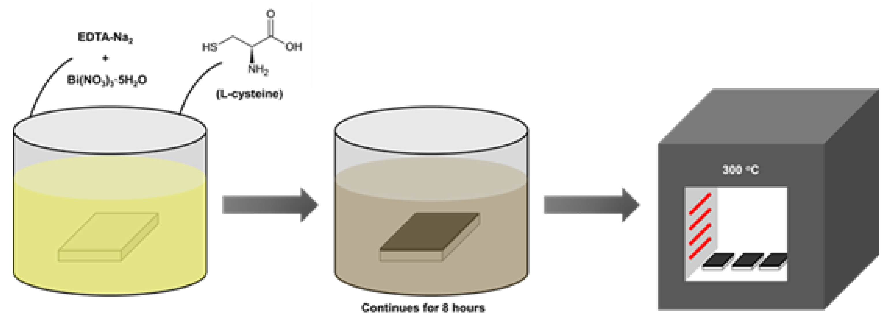
Figure 2.
XRD patterns of Bi2S3 films obtained on FTO slides before annealing and FTO glass slide.
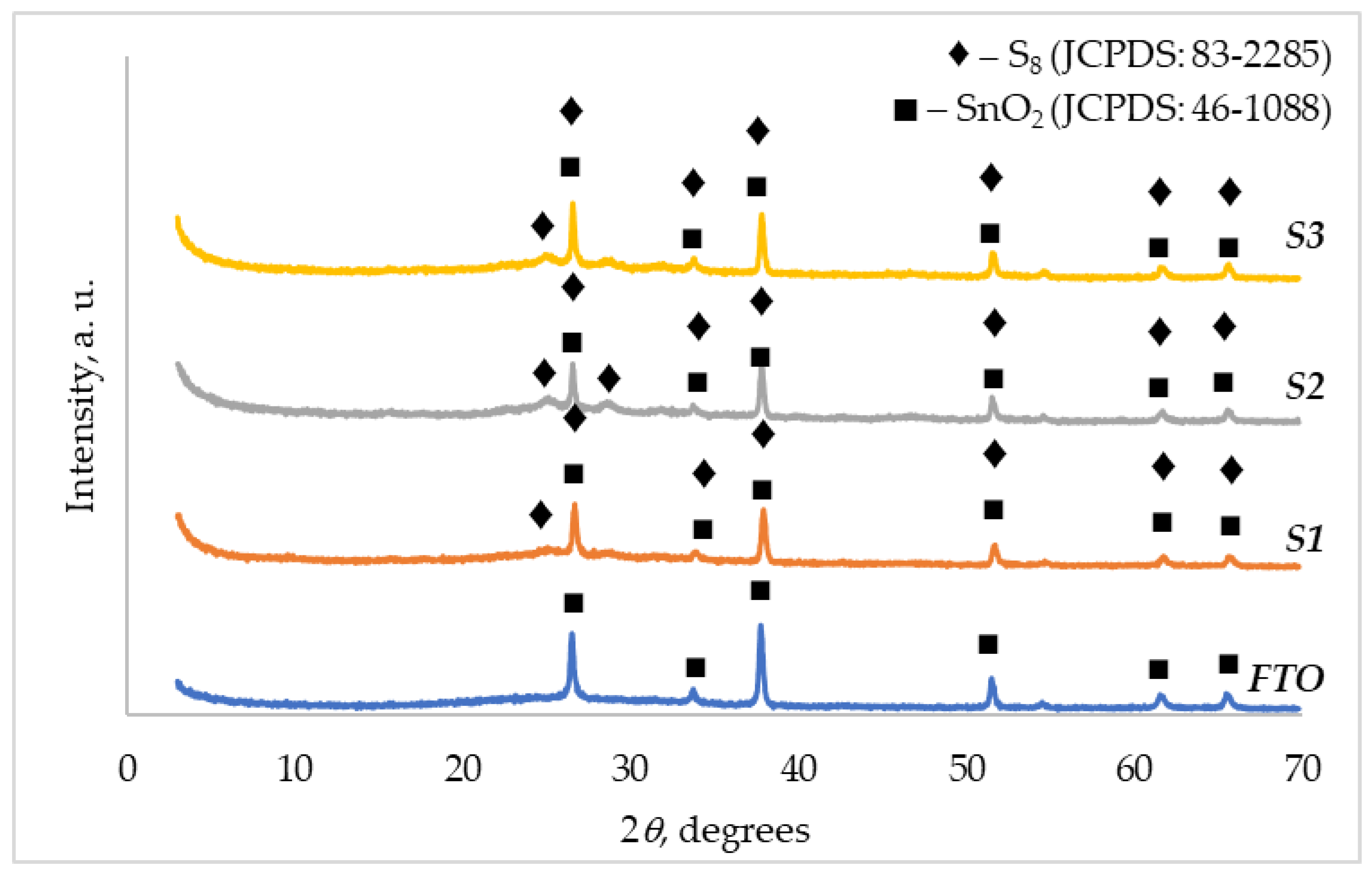
Figure 4.
Corresponding SEM surface images of Bi2S3 films on FTO slides. High-resolution images of these films are shown in the corresponding insets.
Figure 4.
Corresponding SEM surface images of Bi2S3 films on FTO slides. High-resolution images of these films are shown in the corresponding insets.

Figure 5.
Chemical element maps and representative EDX spectra of FTO slides with Bi2S3 films. The measured atomic percentages of Bi and S in the films are shown in the corresponding insets.
Figure 5.
Chemical element maps and representative EDX spectra of FTO slides with Bi2S3 films. The measured atomic percentages of Bi and S in the films are shown in the corresponding insets.

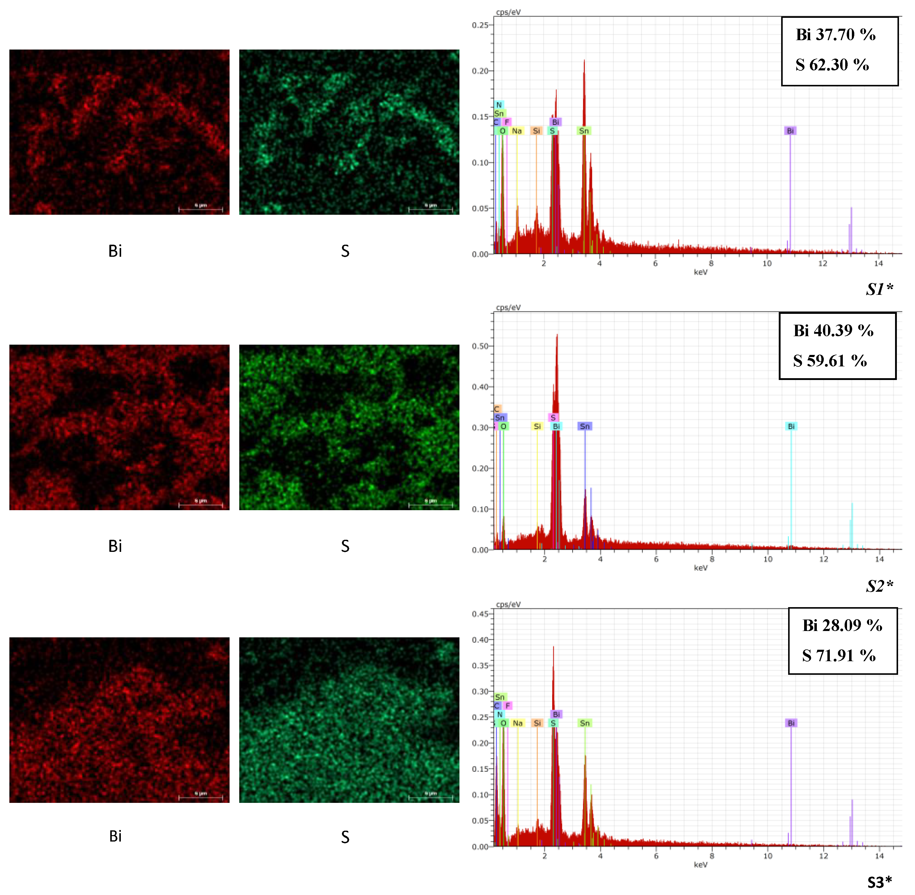
Figure 6.
UV-Vis absorption spectra of the samples S2 and S2*.
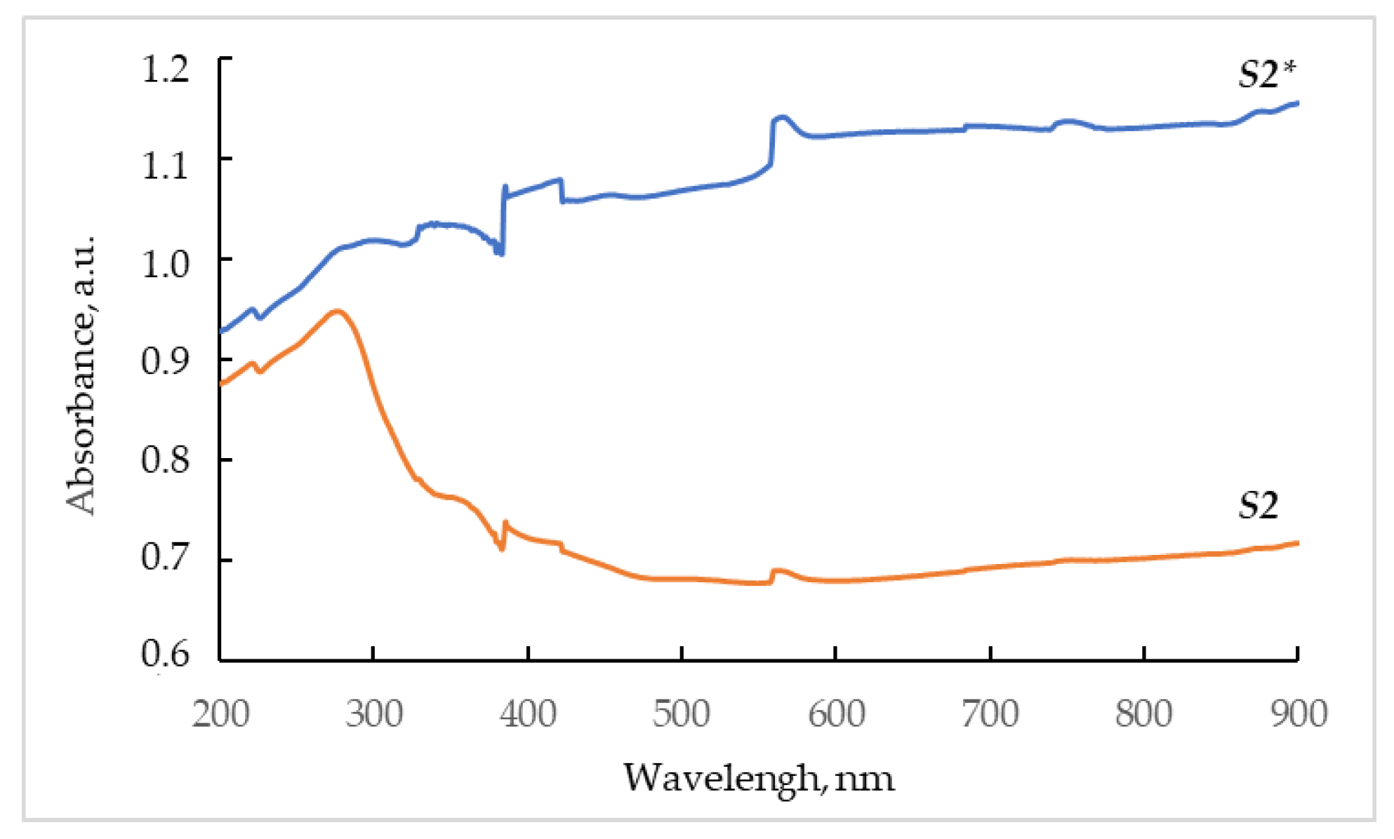

Table 1.
Composition of solutions used in research for formation of Bi2S3 thin films on FTO glass slides.
Table 1.
Composition of solutions used in research for formation of Bi2S3 thin films on FTO glass slides.
| Sample No. | Solution and cocentration, mol/L | L-Cysteine | Total volume of solution, mL | ||
| Bi(NO3)3 × 5H2O | EDTA-Na2- | ||||
| 0.1 | 0.025 | ||||
| Volume of solutions taken for the experiment, mL | Weight, g | Concentration, mol/L | |||
| S1 | 25 | 30 | 1.0 | 0,15 | 55 |
| S2 | 25 | 30 | 1.5 | 0.23 | 55 |
| S3 | 25 | 30 | 2.0 | 0.30 | 55 |
| Concentration of solutions used for the experiment, mol/L | |||||
| 0.0055 | 0.0014 | – | – | 55 | |
Table 2.
XRD 2θ peaks and their assignment of Bi2S3 films formed on FTO glass slides.
| XRD pattern name | Symbol in Figure 2 and Figure 3 – crystallographic phase (JCPDS file number): peak positions 2θ, degrees | |
| S1 | (◆) S8 (JCPDS: 83-2285) | 25.02; 26.66; 33.87; 37.91; 51.69; 61.74; 65.72 |
| S2 | (◆) S8 (JCPDS: 83-2285) | 25.01; 26.59; 28.63; 33.85; 37.81; 51.64; 61.74; 65.70 |
| S3 | (◆) S8 (JCPDS: 83-2285) | 24.98, 26.61; 33.86; 37.89; 51.65; 61.72; 65.71 |
| FTO | (■) SnO2 (JCPDS: 46-1088) | 26.66; 33.87; 37.91; 51.69; 61.74; 65.72 |
| S1* | (◆) S8 (JCPDS: 83-2285) | 26.66; 33.87; 37.91; 51.69; 61.74; 65.72 |
| (●) Bi2S3 (JCPDS: 17-320) | 25.21; 33.83; | |
| S2* | (◆) S8 (JCPDS: 83-2285) | 28.63; 31.89; 37.81; 51.58; 61.64; 65.60 |
| (●) Bi2S3 (JCPDS: 17-320) | 17.69; 25.20; 28.75; 31.89; 52.56 | |
| S3* | (◆) S8 (JCPDS: 83-2285) | 26.57; 33.76; 37.82; 51.60; 61.67; 65.61 |
| (●) Bi2S3 (JCPDS: 17-320) | 25.20 | |
| Scraped film | (●) Bi2S3 (JCPDS: 17-320) | 17.43; 24.98; 28.67; 31.85; 35.51; 39.92; 46.42; 52.52 |
Disclaimer/Publisher’s Note: The statements, opinions and data contained in all publications are solely those of the individual author(s) and contributor(s) and not of MDPI and/or the editor(s). MDPI and/or the editor(s) disclaim responsibility for any injury to people or property resulting from any ideas, methods, instructions or products referred to in the content. |
© 2025 by the authors. Licensee MDPI, Basel, Switzerland. This article is an open access article distributed under the terms and conditions of the Creative Commons Attribution (CC BY) license (http://creativecommons.org/licenses/by/4.0/).
Copyright: This open access article is published under a Creative Commons CC BY 4.0 license, which permit the free download, distribution, and reuse, provided that the author and preprint are cited in any reuse.


