Submitted:
25 February 2025
Posted:
25 February 2025
You are already at the latest version
Abstract
A real-time tunable planar plasmonic waveguide based on voltage-adjustable ferroelectric resonator is designed and investigated. The laminated ferroelectric compound resonator is composed of a ferroelectric layer Ba0.85Ca0.15Zr0.9Ti0.1O3 (BCZT), a PCB layer as well as a localized spoof plasmonic metal layer, where the BCZT layer is benefit for enhancing the voltage tunability in the spoof surface plasmon polaritons (SSPPs) waveguide. The simulated results show that the tuning range of the notch in the transmission curve, generated by the coupling between ferroelectric compound resonator and the plasmonic waveguide, can achieve a variation of up to 8.8% thanks for the large tunability value in the BCZT ferroelectric layer. In addition, the notches are consisted by Fano resonant, whose generation mechanism is elaborately discussed in terms of the temporal coupled mode theory.
Keywords:
ferroelectric compound resonator
; real-time
; voltage tunability
; dielectric properties
; SSPP waveguide
1. Introduction
As well known, the spoof surface plasmon polaritons (SSPPs) concept proposed by J. B. Pendry is a kind of artificial EM wave propagating in corrugated metal, which mimics the natural inherent electron oscillation on metal surface, named surface plasmon polaritons (SPPs) [1,2,3]. Since SSPPs can expand SPPs effect to GHz and THz band through subwavelength engineering in metal, it becomes more flexible and arouses increasing enthusiasm since its proposal. In 2012, Ander Pors et al., proposed the concept of localized spoof surface plasmonic (LSSP), which is the 2D or 3D periodical plasmonic structures on the surface of metal particles, resonating in the excited standing wave mode [4]. The EM field of the resonating LSSP is highly confined near the metal interface with strong enhancement effect and is highly sensitive to the geometry and local dielectric environment [5,6]. For example, in 2021, Zhang Xuanru proposed a ring plasma resonator to achieve both high efficiency and high Q capture mode excitation [7]. Especially, when LSSP work in subwavelength, multipolar plasmonic modes can be activated [8,9,10,11,12], which have sharper resonances than the basic dipole mode, and hence provide higher Q value. Due to these priorities, LSSP have been widely used in optical antennas [13,14,15,16], chemical and biological sensors [17,18,19,20,21], and superlens [22,23,24]. However, previously designed LSSP was mostly static, which means the resonant properties had been solidified once the structure was fabricated. This unitary resonance is not conducive to modern complex communication environments. Thus, the real-time adjustability and experimental flexibility of multiple LSSP become a major challenge.
Some researchers began to employ various kinds of measurements for tuning LSSP. For example, employ PIN diode for electric tuning LSSP [25,26,27]. Yuzan Xiong et al., utilize Yttrium Iron Garnet(YIG) ferrite for magnetically adjusting the ferromagnetic resonance field of the LSSP resonator [28]. Furthermore, varactor diode and micro-electro-mechanical system (MEMS) have also been served as active elements for tuning LSSP [29,30,31]. However, due to the complexity and variability of the communication environment, more regulatory measures need to be continuously expanded.
Ferroelectric materials can realize the exotic regulation of dielectric permittivity with applied DC electric field, which has potential applications in tunable LSSP resonators [32,33,34,35,36]. The advanced features of ferroelectrics include their capability for continuous tunability with high permittivity, low loss and fast responses [37,38,39,40]. It is emphasized that the efficiency of electrical tunability of ferroelectric resonator is larger than that of conventional liquid crystal devices [41,42,43,44], The frequency stability, precision, durability, reliability and vibration resistance of ferroelectric resonators are obviously superior to MEMS and phase change materials [45,46]. Also, ferroelectric resonators can be flexibly regulated employing structure engineering as well as composition fluctuation [47,48,49,50,51,52]. However, until now, few works have comprehensively exploited the modulation mechanism of the ferroelectric resonator.
In this paper, we use the promising environmentally-friendly ferroelectric Ba0.85Ca0.15Zr0.9Ti0.1O3 (BCZT) for fabricating a LSSP resonator. The exhaustive study on the structure engineering as well as the voltage tunability in BCZT is conducted, which possess high dielectric permittivity as well as low loss at microwave frequency and will be beneficial for the high low insertion loss and compact microwave device [53,54,55,56]. Based on these, a compound ferroelectric LSSP resonator is designed and loaded onto a plasmonic waveguide to fulfill the real time and accurate S parameter regulation. Also, we demonstrate that a multiple Fano modes can be aroused by the feeding of the ultracompact plasmonic structure which can be tailored independently for filtering or sensing applications. A model based on temporal coupled mode theory is provided to describe the triple Fano behaviors, including dipole, quadrupole, hexapole modes, which are all sensitive to the disk refractive index of the LSPR. Since the proposed LSSP is a planar textured, it provides significant flexibility in engineering the resonant properties, which possesses potential applications in compact filtering applications at microwave frequencies.
2. Experiments
The BCZT ferroelectrics were synthesized by plasma activated sintering (PAS) method. The calcined BCZT powders were plasma activated for 30s with the supplied pulsed current before sintering using a PAS device (ED-PAS-111, ELENIX, Japan). The axial pressure during PAS sintering is 50 MPa and the heating rate is 100 oC/min with holding time of 3 min at the sintering temperature of 1250oC. The crystal structure of the BCZT ferroelectric was examined by using a PANalytical Empyrean four-circle diffraction system. In order to test the dielectric properties of the BCZT ferroelectric, a dielectric measurement equipment (ZY6173) loaded with a Keysight fixture 16197A that can work in the frequency up to 3GHz was utilized to test the permittivity and loss tangent of the ferroelectric resonator. Then, a compound resonator was designed employing BCZT and PCB laminated structure, whose dielectric permittivity can be regulated flexibly in a large range by its thickness ratio (see Eq (1) ~ (2)). Finally, the compound resonator was loaded on a SSPPs waveguide for fabricating real time tunable notched filter. The dispersion and Extinction Cross Section (ECS) properties of the BCZT compound resonator as well as the tunability of the notching properties was investigated by CST software simulation. The horizontal plane waves were used to excite from the side of the resonator for the calculation of ECS spectra. The boundary condition was set as an open boundary, select time domain solver with a grid resolution of 1000 nm in every direction of the mesh cell. A plane EM wave in the frequency range of 0 to 7 GHz, propagating in the x direction and with an electric field amplitude of 1 V/m, was employed as an incident source in the ECS investigation. A far-field/RCS monitor was selected to record the field information with the sampling of 700 frequency points.
3. Results and Discussion
3.1. Crystal Structure and Dielectric Properties of BCZT Fer-Roelectric
Figure 1 presents the X-ray diffraction (XRD) patterns of the BCZT ferroelectric sintered at 1250oC. The indexed diffraction peaks indicate that the ferroelectric display single phase without any impurity. The inset of Figure 1 depicts the cross sections grain morphology of the as-sintered BCZT ferroelectric. The well-densified grain structure and the even distributed grain size illustrate an optimized sintering condition at 1250oC. Also, the BCZT ferroelectric crystallized in trigonal-tetragonal morphotropic phase boundary (MPB) region at room temperature with the small full width at half-maximum (FMHW), which suggests the excellent crystallinity of the BCZT ferroelectric and will be beneficial for the large permittivity as well as tunability of the subsequent ferroelectric resonator.
In order to construct a tunable microwave device, the dielectric properties as well as the turnability of the BCZT resonator should be declared firstly. Therefore, we begin to investigate the dielectric permittivity as well as the unloaded quality factor of BCZT ferroelectric ceramic at 0.1GHz~1 GHz frequency range, the results are exhibited in Figure 2.
As can be viewed, the BCZT ceramic has a stable permittivity in a wide range of frequency from 0.1 GHz to 1 GHz, and the permittivity at 1GHz frequency band is around 190. The other important issue for ferroelectric devices, the loss tangent of BCZT dielectric in GHz band ranges from 4.0×10⁻⁴ to 6.3×10⁻⁴. The voltage tunability of the BCZT ferroelectric can be refereed by the data reported by D. Mercier et. al [57,58], where 75% capacitance tuning is obtained in the Pt/BCZT/Pt heterostructure system under the biased voltage of 20V. Our previous work on the dielectric tunability of BCZT heterostructure system also shows larger than 60% capacitance tunability [56]. The large permittivity as well as the high tunability of the BCZT ferroelectric will be beneficial for the following design of large tunability in the ferroelectric compound resonator.
3.2. Crystal Structure and Dielectric Properties of BCZT Fer-Roelectric
The following design of LSSP resonator will be started with the design of a compound tunable ferroelectric substrate. As shown in Figure 3, a bilayer compound substrate was constructed using laminated BCZT and PCB substrate. Then the LSSP metal structure was printed on the surface of the compound substrate. Therefore, the substrate permittivity of the LSSP resonator can be flexibly adjusted by applied voltage. According to the superposition principle of EM theory, the final effective permittivity of the compound substrate can be designed by controlling the relative thickness ratio of each layer, as depicted in Eq. (1) and (2) :
Where εi, hi, Pe,i (i = 1, 2, 3) refer to the permittivity, laminated thickness, and filling coefficient of the ith layer in the LSSP resonator respectively. As can be seen from Figure 3(b), since the value of the dielectric permittivity of the whole substrate employed in the simulation is actually an equivalent average value, whose equivalent dielectric permittivity can be adjusted by Pe,i value locating between 0 and 1:
From the above equation, it can be revealed that precise adjustment of the equivalent dielectric permittivity of the resonator can be achieved by judiciously designing the thickness and filling coefficient of each layer in the composite LSSP. For example, when the compound substrate is composed of two layers, where the lower layer is PCB dielectric with the permittivity of 2.2 and thickness of h1= 0.5 mm, and the upper layer composes of BCZT ferroelectric with permittivity being 190 in the working frequency range and with the thickness of h2=0.0054 mm. Then, the permittivity of the compound substrate can be calculated from Eq. (1) and (2), and the result exhibits an equivalent permittivity value of 3.5. Then, as the applied voltage loaded on BCZT layer, it permittivity will experience 60% reduction, and the equivalent permittivity of the compound substrate will becomes 2.9. We numerically compared the ECS properties of the LSSP resonator with the compound substrate and with a single substrate of the equivalent permittivity, as illustrated in Figure 3 (f). The result reveals that the two LSSP resonators with the above two different substrates actually possess similar ECS properties, which indicates the equivalence of the two substrates and verifies our validity in the design strategy of the compound tunable ferroelectric substrate. Also, it is worthy to point out that although the regulation range employed in the LSSP ferroelectric resonator is ranged from 3.5 to 2.9, which is similar to that of the nematic liquid crystals [38], the former actually possesses a larger regulation range than that of the latter since the permittivity variation range of the former can be adjusted by the thickness ratio in the laminated composition.
Bearing the above substrate equivalence in mind, the LSSP can be constructed on a single equivalent substrate in stead of the compound substrate for convenience in the following calculation model. As depicted in panels a and b of Figure 4, the configuration of the LSSP resonator consists of three parts, the upper layer is composed of two disjoint electrodes, the middle layer is the equivalent substrate with permittivity of ε1=3.5 and thickness of t=0.65 mm and the bottom layer is composed of a metal disk with radius r1 and six evenly distributed metal spokes. Figure 4 (c) shows the unit structure diagram of the LSSP resonator, where the geometric parameters are listed in Table 1. The top electrode is composed of two parallel and nonintersecting rectangular metals with each metal electrode has a width of 0.06 mm and a gap being 0.7 mm. The permittivity of ε1 can be regulated by applying voltage at both ends of the electrode. The metal electrode is annealed copper with the thickness of 0.018 mm.
The resonant mode of the LSSP can be essentially understood as a standing wave mode propagating in a waveguide with circular arranged periodic units. When the disk circumference L of the LSSP resonator is equal to an integer n multiple the effective wavelength of the propagating mode, the standing wave resonance will be aroused [53]. Thus, the dipole mode, quadrupole mode, and hexapole mode can be excited, where the three modes represent n=1, 2 and 3 respectively and the wave vector kLSSP of the LSSP resonator can be described as:
Then, the dispersion characteristics of LSSP resonator as a function of the permittivity is investigated. The simulated results illustrate that when ε1=3.5, the asymptotic frequency is slightly lower than that of ε1=2.9, deviating further from the light line, as shown in Figure 4(d). Since the distance from the dispersion curve to the light reflects the constraint ability on the field, it means that as the increase of ε1, the constrained field gradually increases, resulting in less radiation loss of the LSSP resonator. Moreover, according to the dispersion relationship of the LSSP unit structure and its circumference, it can be seen that when the permittivity is 3.5, the dipole frequency of the resonator should appear at 3.6 GHz, while the quadrupole and the hexapole resonance appear at 5.68 GHz and 6.35 GHz respectively in terms of Eq. (3). It can be seen that the calculated resonances according to the dispersion curve correspond quite well with the resonant peaks in the ECS spectra, as exhibited in Figure 3(a).
3.3. Tunability of SSPP Waveguide Loaded with BCZT LSSP Resonator
According to above investigation, it is conducive to the higher tunability of εr in BCZT compound resonator, which, in turn will be beneficial for the following tunability of the plasmonic waveguide. Figure 5 presents the plasmonic waveguide with the BCZT compound resonator loaded symmetrically along the center of SSPPs waveguide. The transmitted power distribution was numerically monitored in the x-y plane 0.5 mm above the coupled LSSP resonator at the resonant frequencies. The plasmonic waveguide is settled on Rogers RT5880 substrate with the substrate thickness of 0.5 mm, the permittivity of 2.2 and the loss tangent being 0.0009.
After loading LSSP resonator, we conducted numerical simulation on the S parameter of the filter, and the results are shown in Figure 5. The power flow distribution forms counter-clockwise closed loops in LSSP and the first three excited resonant modes are dipole, quadrupole and hexapole resonant modes, as depicted in Figure 5(c). Also, when the dielectric permittivity of the resonator is varied from 3.5 to 2.9, the entire resonance peak position undergoes a blue shift, where the resonant frequency of the dipole mode shifts from 3.44 GHz to 3.65 GHz, with a blue shift of 210 MHz, or a 6.1% controllable range. Meanwhile, the resonant frequency of the quadrupole mode shifts from 5.39 GHz to 5.71 GHz, with a blue shift of 320 MHz or a regulation range of 5.9%, and the hexapole mode shifts from 6.07 GHz to 6.44 GHz, with a tuning range of 6.1%, which is well consistent with the variation pattern of the ECS spectra of the LSSP resonator illustrated in Figure 3(a). Also, the transmission properties show that the excited dipole, the quadrupoles as well as the hexapole of the loaded LSSP resonator are all Fano resonance because of the asymmetrically distributed resonant line shape. Thus, in the spectral domain, the interference between these plasmonic modes can be expressed with an analytical Fano interference model to fit the spectral lines as :
Where ω0 represents the Fano resonant frequencies, Γ is the resonance line width, T0 characterizes the background scattering parameter, A0 is the coupling parameter between the background and the Fano resonances, and q depicts the Breit-Wigner-Fano parameter, which determines the asymmetry of the resonance spectral line.
The fitting spectral line utilizing the analytical Fano format as well as the simulated spectra are shown in the red and black line respectively in Figure 6. As can be seen, a well matched spectra within the three oscillations (n = 1, 2, 3) can be obtained for the LSSP structure. The resonant frequencies of the dipole, quadrupole and the hexapole modes center at 3.43 GHz, 5.39 GHz and 6.06 GHz, respectively, and the corresponding line widths of the modes are 0.0125 GHz, 0.078 GHz and 0.045 GHz respectively. Thus, the Q value of the resonator can be calculated using the following formula:
The results show that Q values of the dipole, quadrupole and hexapole modes of the LSSP resonator can be calculated as 275, 80 and 135, respectively.
3.4. Coupling Mechanism Between BCZT LSSP Resonator and SSPP Waveguide
To reveal the formation of Fano response of the LSSP resonator, the coupling mechanism of the near-field EM between the three Fano modes and the SSPP modes in plasmonic waveguide is investigated in terms of temporal coupled mode theory (TCMT). The excited Fano modes should stem from the interference of the two transmission paths, as illustrated in Figure 7. An equivalent network is therefore employed to describe the EM field coupling characteristics between the two plasmonic structures, as illustrated in the inset of Figure 7.
A dielectric loss as well as weak radiative loss of the LSSP resonator is considered azimuthally as a resistance R, where the amplitude damping factor in LSSP is denoted as γ. The normalized EM power due to the interference of the two transmission paths can thus be depicted as:
Then, the transmission coefficient E2/E1 can be deduced as:
Where t represents the coupling through nonradiative damping channels and r describes the coupling process from LSSP resonator back to the plasmonic waveguide, j stands for imaginary unit and E stands for electric field strength. For the lossless coupling process between the SSPPs waveguide and LSSP resonator, we assume t2 + r2 = 1. The rotated phase delay θ distributed along the azimuthal direction of the LSSP resonator is in the range of 0 to 2π for the dipole Fano mode. In terms of the low loss of BCZT substrate in the LSSP resonator, we consider the weak value of R in the equivalent circuit, and set [54], where represents the dipole resonant frequency, t = 0.996 to fit the normalized transmission coefficient.
It evidently indicates the coupling effect between SSPPs waveguide and the LSSP resonator can deeply trap the power flow, appearing strong band notch in the transmission spectrum, as exhibited in Figure 7. Also, the theoretical calculated real part ratio ǀE2/E1ǀ in Eq. (9), standing for transmission intensity ratio, matches quit well with the numerical simulated one. It can thus be validated that the asymmetric field fed by the SSPP waveguide could lead to a unidirectional EM coupling into the LSSP resonator, and therefore create an asymmetric resonant line shape, forming the Fano resonant.
4. Conclusions
In summary, a LSSP resonator with BCZT compound ferroelectric substrate is designed and employed for the tunability of SSPP waveguide. Results show that high dielectric tunability can be achieved in the BCZT laminated structure, which is beneficial for the deep tunability of the notch in the plasmonic waveguide. When a pair of mirrorly-symmetrical LSSP resonators is coupled to the SSPPs WG, the central frequency of the notch can be dynamically adjusted in real-time by about 8.8% due to the high dielectric tunability of BCZT. In addition, the notch generated by the plasmonic coupling enables excitation of triple Fano resonances, which stems from a unidirectional EM coupling between the LSSP resonator and the SSPP waveguide.
The method provides a new idea for the compact physical size, minimal insertion loss, large tunability and real-time flexible regulation in notch filter scenarios. Also, since the proposed LSSP is a planar textured disk, it is more flexible in engineering Fano line shape, which can be of practical interest for a variety of applications including enhanced biosensing, on-chip communication, and optical information processing.
Author Contributions
Conceptualization, Mingzhe Hu and Chuanbin Wang; methodology, Jiaxiong Shen and Shun Lei; validation, Jiaxiong Shen and Chaobiao Zhou; formal analysis, Shengyun Luo and Chaobiao Zhou; investigation, Chaobiao Zhou and Chuanbin Wang; data curation, Shun Lei and Shengyun Luo; writing—original draft preparation, Jiaxiong Shen; writing—review and editing, Mingzhe Hu and Chuanbin Wang; supervision, Mingzhe Hu; project administration, Chuanbin Wang; funding acquisition, Mingzhe Hu. All authors have read and agreed to the published version of the manuscript.
Data Availability Statement
The data generated by the process can be found in the text, and no additional data needs to be added.
Acknowledgments
This work was financially supported by the National Natural Science Foundation of China (62261008), the High Level Innovative Talent Project of Science and Technology Department of Guizhou Province (GCC2023086) and the Fundamental Research Funds for the Central Universities (WUT: 2019Ⅲ029).
Conflicts of Interest
The authors declare that they have no known competing financial interests or personal relationships that could have appeared to influence the work reported in this paper.
References
- Pendry, J., B.; Holden, A., J.; Stewart, W., J. and Youngs, I. Extremely low frequency plasmons in metallic mesostructures. Physical review letters. 1996, 76, 4773. [Google Scholar] [PubMed]
- Zayats, A.V. ; Smolyaninov, I, I. ; Maradudin, A, A. Nano-optics of surface plasmon polaritons. Physics reports. 2005, 408, 131–314. [Google Scholar]
- Garcia-Vidal, F, J. ; Martin-Moreno, L and Pendry, J, B. Surfaces with holes in them: new plasmonic metamaterials. Journal of optics A: Pure and applied optics. 2005, 7, S97.
- Pendry, J, B. ; Martin-Moreno, L and Garcia-Vidal, F, J. Mimicking surface plasmons with structured surfaces. Science. 2004, 305, 847–848.
- Ritchie, R. ; H Plasma losses by fast electrons in thin films. Physical review. 1957, 106(5), 874. [Google Scholar]
- Liebsch, A. Electronic excitations at metal surfaces. Springer Science & Business Media. 2013.
- X, Zhang and T, J, Cui. Deep-subwavelength and high-Q trapped mode induced by symmetry-broken in toroidal plasmonic resonator. IEEE Transactions on Antennas and Propagation 69. 2020, 2122-2129.
- Maier, S. ; A Plasmonics: fundamentals and applications. New York: springer. 2007.
- Baimuratov, A, S.; Tepliakov, N, V.; Gun’ko, Y, K.; Baranov, A, V and Fedorov, A, V. Mixing of quantum states: A new route to creating optical activity. Scientific reports. 2016, 6(1), 5.
- Homola, J. Present and future of surface plasmon resonance biosensors. Analytical and Bioanalytical chemistry. 2003, 377, 528–539. [Google Scholar] [CrossRef]
- Pan, L.; Wu, Y.; Wang, W. ; Wei, Y and Yang, Y. A flexible high-selectivity single-layer coplanar waveguide bandpass filter using interdigital spoof surface plasmon polaritons of bow-tie cells. IEEE transactions on plasma science. 2020, 48, 3582–3588. [Google Scholar]
- Jaiswal, R, K. ; Pandit, N and Pathak, N, P. Spoof plasmonic-based band-pass filter with high selectivity and wide rejection bandwidth. IEEE photonics technology letters. 2019, 31, 1293–1296.
- Wang, J. ; Zhao, L and Hao, Z, C. A band-pass filter based on the spoof surface plasmon polaritons and CPW-based coupling structure. IEEE access. 2019, 7, 35089–35096. [Google Scholar]
- Guo, Y, J.; Xu, K, D.; Deng, X.; Cheng, X and Chen, Q. Millimeter-wave on-chip bandpass filter based on spoof surface plasmon polaritons. IEEE electron device letters. 2020, 411165-1168.
- Zhang, D.; Sun, Y.; Zhang, K. ; Wu, Q and Jiang, T. Short-circuited stub-loaded spoof surface plasmon polariton transmission lines with flexibly controllable lower out-of-band rejections. Optics letters. 2021, 46, 4354–4357. [Google Scholar]
- Yang, Z.; Zhang, B. ; Chen, W and Yang, T. Rejection of spoof SPPs using the second resonant mode of vertical split-ring resonator. IEEE microwave and wireless components letters. 2018, 29, 23–25. [Google Scholar]
- Li, W.; Qin, Z.; Wang, Y. ; Ye, L and Liu, Y. Spoof surface plasmonic waveguide and its band-rejection filter based on H-shaped slot units. Journal of Physics D: Applied physics. 2019, 52, 365303. [Google Scholar]
- Yan, D.; Li, X.; Ma, C. Terahertz refractive index sensing based on gradient metasurface coupled confined spoof surface plasmon polaritons mode. IEEE Sensors Journal. 2021, 22, 324–329. [Google Scholar]
- Kumari, A. ; Singh, S, P. ; Tiwari, N, K. Design of a differential spoof surface plasmon sensor for dielectric sensing and defect detection. IEEE sensors journal. 2022, 22, 3188–3195. [Google Scholar]
- Fu, J, H. ; W, J, Wu.; Wang, D, W. High-sensitivity microfluidic sensor based on quarter-mode interdigitated spoof plasmons. IEEE Sensors Journal. 2022, 22, 23888–23895.
- Dai, L, H. ; Zhao, H, Z.; Zhao, X. Flexible and printed microwave plasmonic sensor for noninvasive measurement. IEEE Access. 2020, 8, 163238–163243.
- Li, W.; Qin, Z.; Wang, Y. ; Ye, L and Liu, Y. Spoof surface plasmonic waveguide and its band-rejection filter based on H-shaped slot units. Journal of Physics D: Applied physics. 2019, 52(36), 365303.
- Xu, K, D.; Lu, S.; Guo, Y, J and Chen, Q. High-order mode of spoof surface plasmon polaritons and its application in bandpass filters. IEEE Transactions on Plasma Science. 2020, 49(1),269-275.
- Mira, F. ; Mateu, J and Collado, C. Mechanical tuning of substrate integrated waveguide filters. IEEE Transactions on Microwave Theory and Techniques. 2015, 63(12), 3939–3946. [Google Scholar]
- C, Zhang and Y, J, Zhou. Electronically controlled spoof localized surface plasmons on the corrugated ring with a shorting pin. Journal of Modern Optics. 2018, 65(13), 1535–1541.
- Ding, J.; Zhao, P.; Chen, H. ; et al. Ultraviolet photodetectors based on wide bandgap semiconductor: a reviewJ. Applied Physics A. 2024, 130(5), 350.
- Pande, S.; Patil, D.; Kumar, A. ; et al. Design of a metasurface loaded with RF varactor and PIN diode integration dual-band reconfigurable antenna for bluetooth, Wi-Fi, WLAN and wireless 5G applications. Physica Scripta. 2025, 100(2), 025537-025537.
- Y, Z, Xiong. ; A, Christy and Y, Dong. Combinatorial split-ring and spiral metaresonator for efficient magnon-photon coupling. Physical review applied. 2024, 21, 034034.
- J, Ma. ; J, M, Hu.; Z, Li and C, W. Recent progress in multiferroic magnetoelectric composites: from bulk to thin films. Adv. Mater. 2011, 42(18), 1062-1087. [Google Scholar]
- S, Q, Li.; C, H, Du. Efficient magnetic-coupling excitation of LSSPs on high-Q multilayer planar-circular-grating resonators. Optics Express. 2021, 29(16), 25189-25201.
- B, Zhu.; M, Z, Hu. Plasmonic dual-band waveguide with independently controllable band-notched characteristics. Applied Physics Express. 2023, 16(8), 086001.
- R, Ramesh and N, A, Spaldin. Multiferroics: progress and prospects in thin films. Nat. Mater. 2007, 6 (1), 21-29.
- G, Zhang. Multiferroic properties of CaMn7O12. Phys. Rev. B. 2011, 84(17), 174413.
- J, Lou. Tunable spoof surface plasmon polariton transmission line based on ferroelectric thick film. Applied Physics A. 2019, 125(10), 737.
- Miranda, F, A.; Subramanyam, G.; Vankeuls, F, W and Romanofsky, R, R. Design and development of ferroelectric tunable microwave components for Ku- and K-band satellite communication systems. ZEEE Trans. Microw. Theory Tech. 2000, 48 (7), 1181-1189.
- G, Schileo.; C, Pascual-Gonzalez.; M, Alguero and I, M. Multiferroic and magnetoelectric properties of Pb0.99 [Zr0.45Ti0.47(Ni1/3Sb2/3)0.08] O3-CoFe2O4 multilayer composites fabricated by tape casting. J. Eur. Ceram. Soc. 2018, 38 (4), 1473-1478.
- W, Liu and X, Ren. Large piezoelectric effect in Pb-free ceramics. Phys. Rev. Lett. 2009, 103 (25), 257602.
- C, W, Nan. ; M, I, Bichurin.; S, Dong., Ed.; D, Viehland and G, Srinivasan. Multiferroic magnetoelectric composites: Historical perspective, status, and future directions. J. Appl. Phys. 2008, 103 (3), 03110. [Google Scholar]
- T, Li. ; F, Zhang.; H, Fang.; K, Li and F, Yu. The magnetoelectric properties of La0.7Sr0.3MnO3/BaTiO3 bilayers with various orientations. J. Alloy. Compd.2013, 560 (4), 167-170.
- T, Li. ; H, Wang. ; D, Ma.; K, Li and Z, Hu. Influence of clamping effect in BaTiO3 film on the magnetoelectric behavior of layered multiferroic heterostructures. Mater. Res. Bull. 2019, 115, 116–120. [Google Scholar]
- L, W, Martin and R, Ramesh. Multiferroic and magnetoelectric heterostructures. Acta Mater. 2012, 60 (6-7), 2449-2470.
- Y, K, Fetisov and G, Srinivasana. Electric field tuning characteristics of a ferrite-piezoelectric microwave resonator. Appl. Phys. Lett. 2006, 88, 143503.
- A, Ustinov. ; G, Srinivasan and B, A, Kalinikos. Ferrite-ferroelectric hybrid wave phase shifters. Appl. Phys. Lett. 2007, 90, 031913.
- C, Pettiford. ; S, Dasgupta.; J, Lou.; S, D, Yoon and N, X, Sun. Bias field effects on microwave frequency behavior of PZT/YIG magnetoelectric bilayer. IEEE Trans. Magn. 2007, 43, 3343.
- Zine-El-Abidine. A tunable radio frequency MEMS inductor using MetalMUMPs. Journal of Micromechanics and Microengineering. 2007, 17(11), 2280.
- G, Hummel. Reconfigurable piezoelectric MEMS resonator using phase change material programmable vias. Journal of Microelectromechanical Systems. 2015, 24(6), 2145–2151.
- J, Wang.; Z, Li.; J, Wang.; H, He and C, Nan. Effect of thickness on the stress and magnetoelectric coupling in bilayered Pb (Zr0.52Ti0.48) O3-CoFe2O4 films. J. Appl. Phys. 2015, 117(4), 759.
- K, B, Fan. Active and tunable nanophotonic metamaterials. Nanophotonics. 2022, 11(17), 3769–3803.
- Y, Q, Dai.; J, M, Dai.; X, W, Tang.; K, J, Zhang.; X, B, Zhu.; J, Yang and Y, P, Sun. Thickness effect on the properties of BaTiO3-CoFe2O4 multilayer thin films prepared by chemical solution deposition. J. Alloy. Compd. 2014, 587(7), 681-687.
- N, A, Pertsev. Effect of mechanical boundary conditions on phase diagrams of epitaxial ferroelectric thin films. Phys. Rev. Lett. 1998, 80(9), 1988–1991.
- V, Ion.; F, Craciun.; N, D, Scarisoreanu.; A, Moldovan.; A, Andrei.; R, Birjega and C, Ghica. Impact of thickness variation on structural, dielectric and piezoelectric properties of (Ba, Ca) (Ti, Zr) O3 epitaxial thin films. Sci. Rep. 2018, 8(1), 2056.
- Pei, H.; Zhang, Y.; Guo, S.; Ren, L. ; Yan, H and Luo, B. Orientation-dependent optical magnetoelectric effect in patterned BaTiO3/La0. 67Sr0. 33MnO3 heterostructures. ACS applied materials & interfaces. 2018, 10(36) 30895-30900.
- S, B, Li. ; C, B, Wang.; Q, Shen and L, M Zhang. Enhanced dielectric properties in Ba0.85Ca0.15Zr0.10Ti0.90O3/La0.67Ca0.33MnO3 laminated composite. Scripta Mater. 2018, 144, 40–43.
- M, Z, Hu.; S, Li and C, B, Wang. Orientation-dependent multiferroic properties in BCZT/LCMO thin films. Ceram. Int. 2021, 103(12), 385-991.
- Mercier, D.; Niembro-Martin, A.; Sibuet, H. ; Baret, C and Chautagnat, J. X band distributed phase shifter based on Sol-Gel BCTZ varactors. 2017 European Radar Conference (EURAD), IEEE. 2017, 382-385.
- Mercier, D. ; Sibuet, H and Dieppedale, C. et al. 8 to 13 GHz tunable filter based on sol-gel BCTZ varactors. 2017 IEEE Asia Pacific Microwave Conference (APMC), IEEE. 2017, 686-689.
- X, R, Zhang. ; R, T, Yan and T, J, Cui. High-FoM Resonance in Single Hybrid Plasmonic Resonator via Electro-Magnetic Modal Interference. IEEE Transactions on Antennas and Propagation. 2020, 8, 1–1.
- M, Z, Hu. ; H, S, Gu.; X, C, Chu.; J, Qian and Z, Xia. Crystal structure and dielectric properties of (1− x) Ca0. 61Nd0. 26TiO3+ xNd (Mg1/2Ti1/2) O3 complex perovskite at microwave frequencies. Journal of Applied Physics. 2008, 104, 124104.
Figure 1.
XRD pattern and corresponding SEM image (the inset) of the BCZT ferroelectric sintered at the optimized temperature of 1250oC.
Figure 1.
XRD pattern and corresponding SEM image (the inset) of the BCZT ferroelectric sintered at the optimized temperature of 1250oC.
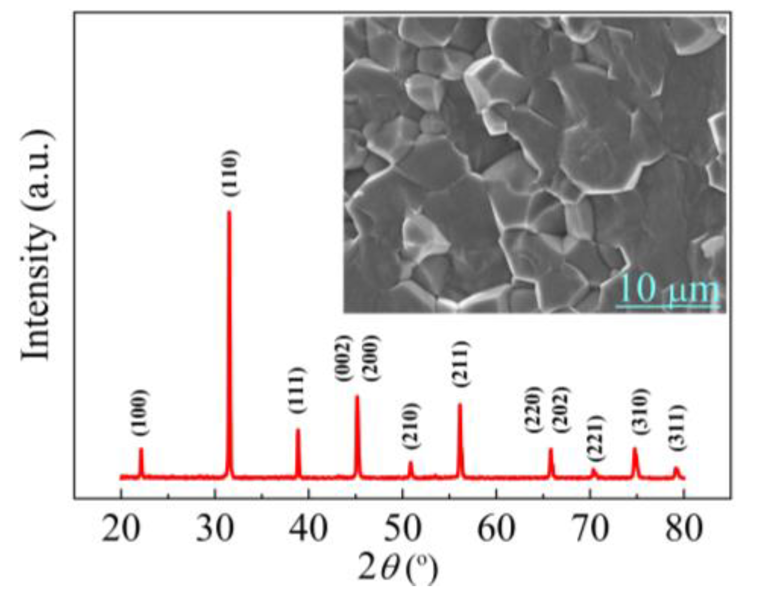
Figure 2.
The dielectric permittivity and loss tangent (tanδ) of BCZT ferroelectric in 0.1GHz~1GHz frequency range.
Figure 2.
The dielectric permittivity and loss tangent (tanδ) of BCZT ferroelectric in 0.1GHz~1GHz frequency range.
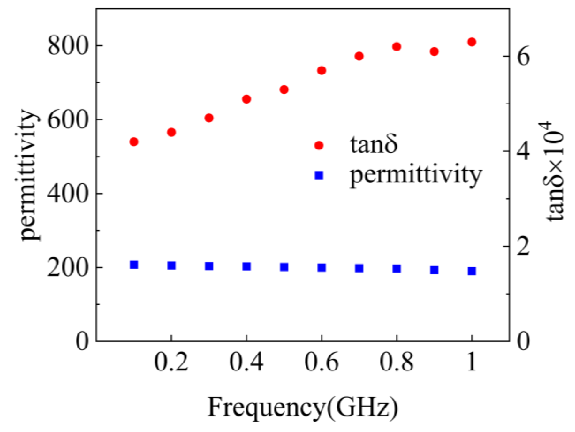
Figure 3.
(a) The variation of the simulated ECS spectra with the permittivity ε1 of the substrate (The inset shows the excitation direction of the plane wave), (b)The com-parison of ECS spectra of the ferroelectric composite die-lectric resonator vs the effective single layer LSSP reso-nator. The inset is the schematic diagram of the composite substrate, which consists of two layers. The upper layer is the BCZT ferroelectric with permittivity of 190 and lower layer is PCB dielectric with a permittivity of 2.2. The spoke electrodes of the LSSP resonator is on the surface. (c) and (d) represent the internal electric and magnetic field distribution diagram at the three resonant peaks marked as 1 (dipole), 2 (quadrupole) and 3 (hexapole) of the LSSP resonator with ε1=3.5, respectively, (e) and (f) describe the internal electric and magnetic field distribu-tion diagram at the three resonant peaks marked as 1* (dipole), 2* (quadrupole) and 3* (hexapole) of the LSSP resonator with ε1=2.9.
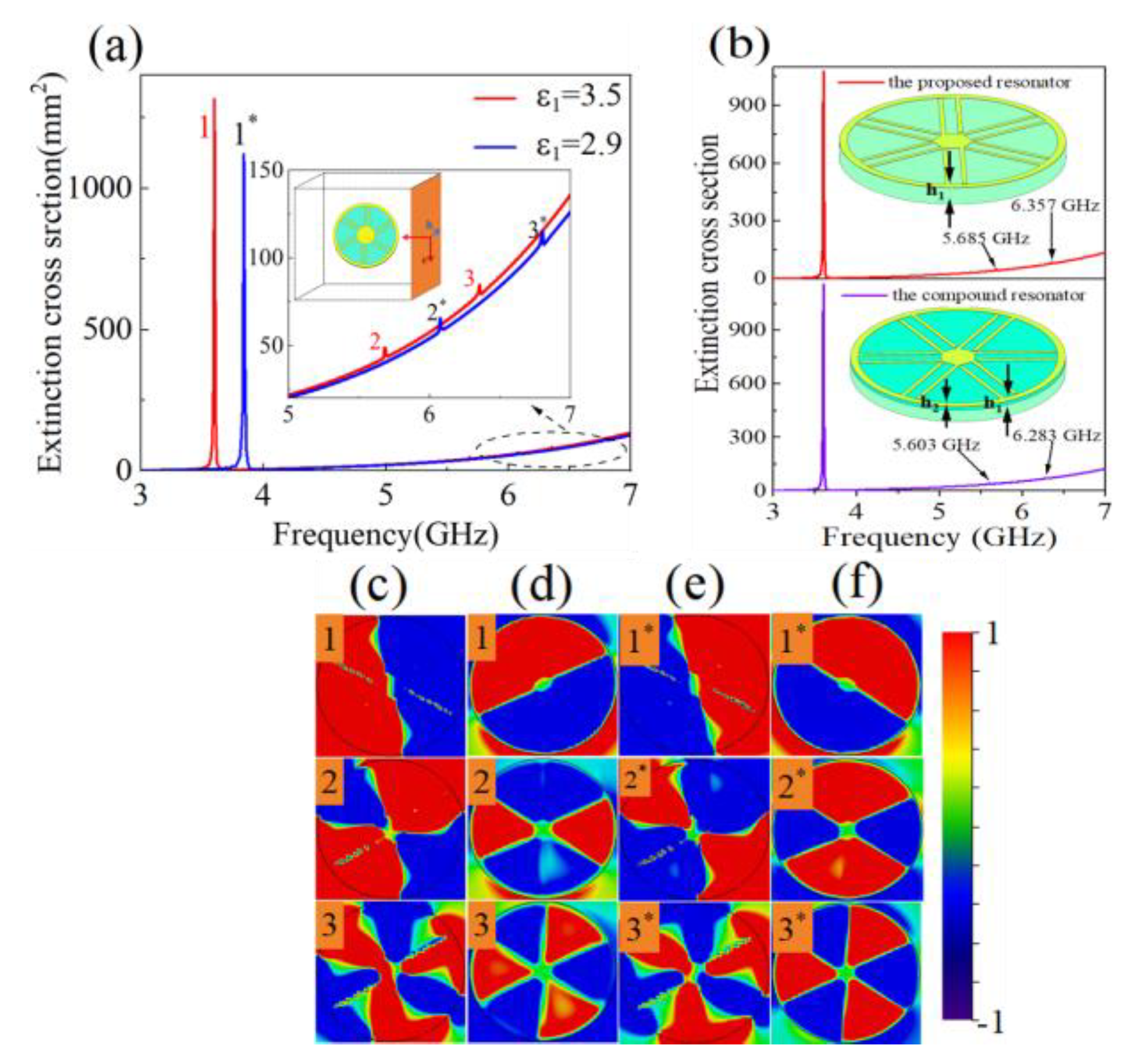
Figure 4.
(a) Schematic diagram of the top of the resona-tor, with the parameters listed in Table 1. (b) Schematic diagram of the bottom of the resonator with the LSSP structure of periodic straight spokes. (c) Local unit struc-ture diagram of the LSSP resonator with the parameters listed in Table 1. (d) Dispersion curve of the LSSP resona-tor with different substrate permittivity ε1. The substrate thickness is 0.5 mm. (e) and (f) The internal electric and magnetic field distribution diagram at three resonant points A, B and C of the LSSP resonator respectively as ε1=3.5.
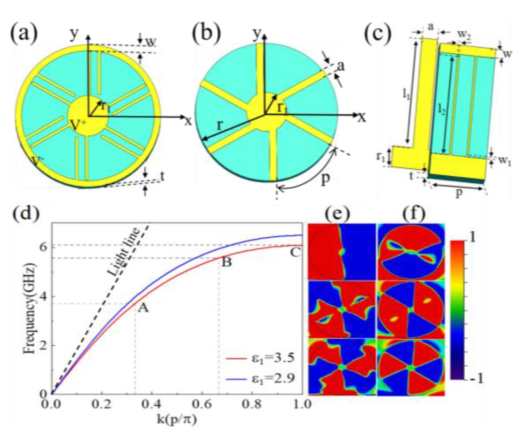
Figure 5.
(a) and (b) The schematic structure of the plas-monic waveguide. (c) the simulated transmission spectra loaded with the BCZT compound resonator. (d) and (e) The internal electric and magnetic field distribution dia-gram at three notched points 1, 2 and 3 respectively as ε1=3.5. (f) and (g)The internal electric and magnetic field distribution diagram at three notched points 1*, 2* and 3* respectively as ε1=2.9.
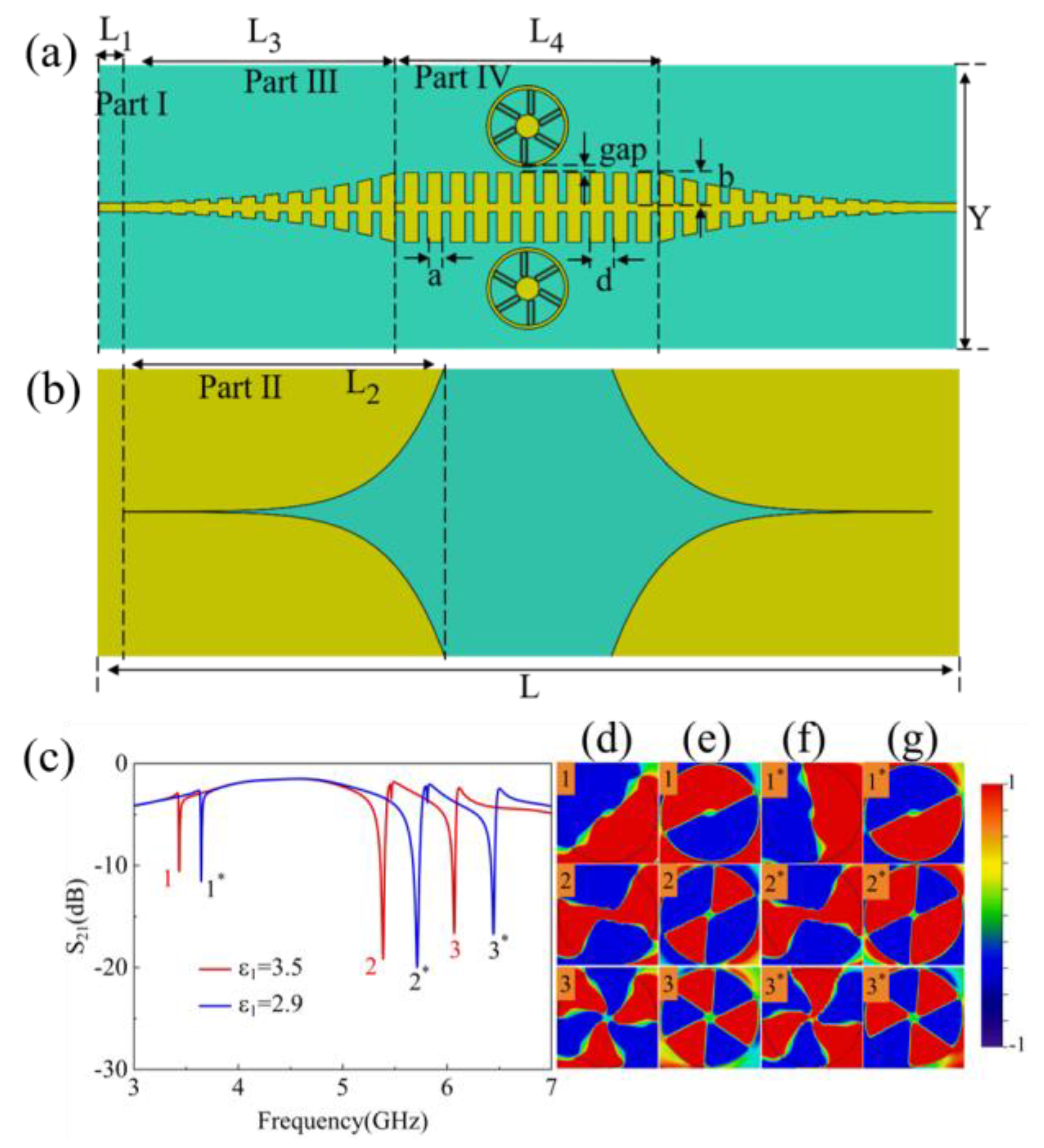
Figure 6.
Simulation and Fano fitting of (a) dipole peak, (b) quadrupole peak and (c) hexapole peak of the LSSP resonator as ε1 = 3.5.
Figure 6.
Simulation and Fano fitting of (a) dipole peak, (b) quadrupole peak and (c) hexapole peak of the LSSP resonator as ε1 = 3.5.
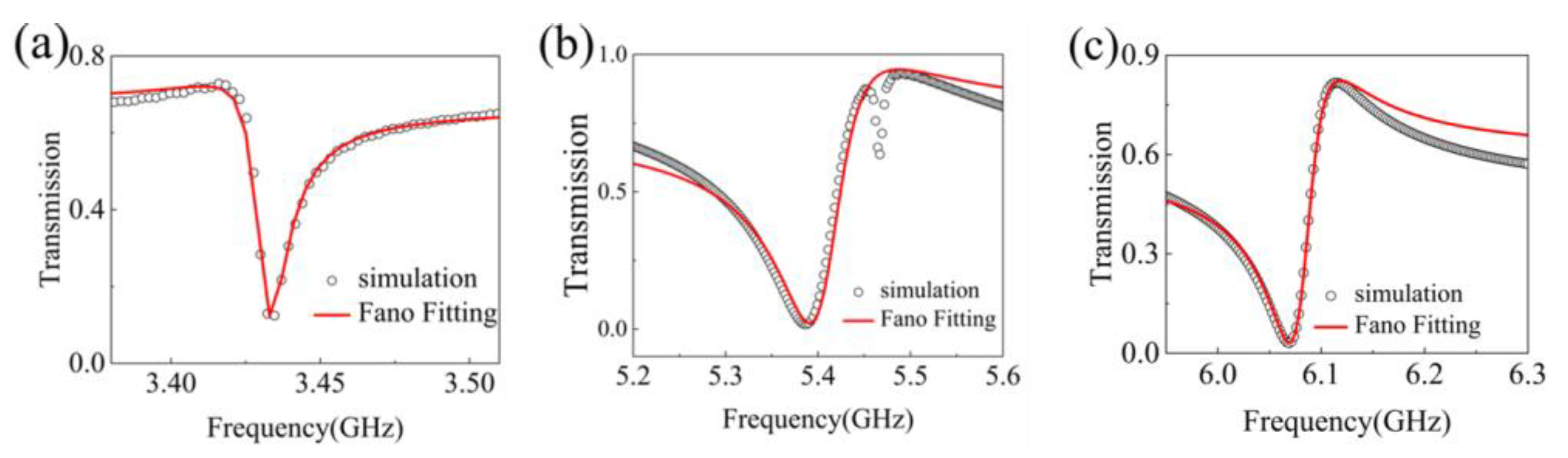
Figure 7.
When ε1 is equal to 3.5, the calculated (blue line) and simulation results (red line) of the real part ǀE2/E1ǀ in terms of TCMT. The inset shows the equivalent network model revealing the near field EM power transferring be-tween the plasmonic waveguide and the LSSP resonator.
Figure 7.
When ε1 is equal to 3.5, the calculated (blue line) and simulation results (red line) of the real part ǀE2/E1ǀ in terms of TCMT. The inset shows the equivalent network model revealing the near field EM power transferring be-tween the plasmonic waveguide and the LSSP resonator.
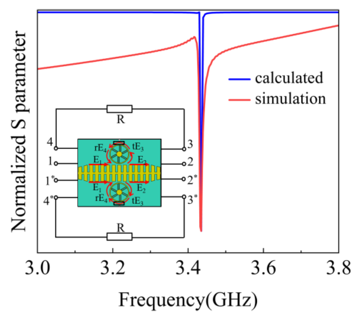

Table 1.
The denotation and physical dimensions of each part of the designed SSPP waveguide loaded with LSSP resonator.
Table 1.
The denotation and physical dimensions of each part of the designed SSPP waveguide loaded with LSSP resonator.
| Structure | Symbol | Size (mm) |
|---|---|---|
| the lower surface metal strip length | l1 | 5.25 |
| the upper metal strip length | l2 | 4.71 |
| the gap between upper center circle and metal strip | w1 | 0.1 |
| the upper surface metal strip width | w2 | 0.08 |
| the upper and lower center metal circle radius | r1 | 1 |
| the upper metal ring width | w | 0.44 |
| the lower surface metal strip width | a | 0.7 |
| the periodic of the circle slots | p | 6.545 |
| the thickness of the dielectric substrate | t | 0.65 |
Disclaimer/Publisher’s Note: The statements, opinions and data contained in all publications are solely those of the individual author(s) and contributor(s) and not of MDPI and/or the editor(s). MDPI and/or the editor(s) disclaim responsibility for any injury to people or property resulting from any ideas, methods, instructions or products referred to in the content. |
© 2025 by the authors. Licensee MDPI, Basel, Switzerland. This article is an open access article distributed under the terms and conditions of the Creative Commons Attribution (CC BY) license (http://creativecommons.org/licenses/by/4.0/).
Copyright: This open access article is published under a Creative Commons CC BY 4.0 license, which permit the free download, distribution, and reuse, provided that the author and preprint are cited in any reuse.


