
Submitted:
14 February 2025
Posted:
17 February 2025
You are already at the latest version
Abstract
Here a graphene-based photodetectors with ability to integrate with various energy thermoelectric, electromagnetic and piezoelectric devices is reported. The fabrication of the proposed device is based on magnetic field assisted pulsed laser deposition (MFPLD) for growth of few layers graphene and intercalated chemical vapor deposition (CVD) graphene grown following by a wet transfer of the layers to the electrode surface. The key influential parameter in the graphene growth such as density and smoothness of surface, as well as the plasma plume particles charge type and velocity have been optimized to obtain the best quality of the graphene and consequently improve the performance of the device. For the electrical contacts a tapered aluminum microelectrode (TAM) has been used to improve the detection of photogenerated carriers during the illumination. The results reveal the acceptable wide band response, leading to a responsivity of up to 0.13 AW-1, quantum efficiency of 9.5% and room temperature specific detectivity of 1.27x10+7 Jones at wavelength of 1700 nm.
Keywords:
Photodetector
; Graphene
; Pulsed laser deposition
; chemical vapor deposition
; tapered aluminum microelectrode
1. Introduction
Photodetectors (PDs), which convert light into electrical signals, play a crucial role in various fields such as data transmission [1], night vision imaging [2], wearable devices [3], military applications [4,5]. For the visible light detection, silicon (Si) photodetectors have been the main platform due to its compatibility with CMOS technology and all the advances occurred in technology for integration with photonic and electronic platforms. The main challenge for Si PDs is due to its fixed band gap width of 1.1 eV and the limited detection range to cover broad band applications beyond visible light region. When it comes to near infrared (NIR) and short–wavelength infrared (SWIR) several material systems have been used for detection; each of those material systems has its own advantages and disadvantages. II-IV material system, and technologically matured mercury–cadmium–telluride (HgCdTe) is capable of detection of the entire infrared spectral range, [6,7,8,9] but certain issues, such as complex material growth and fabrication processes [10,11] are still limiting factors. High performance III-V materials such as InxGa1-xAs compounds photodetectors (if lattice–matched to InP substrate) are great candidate for NIR and SWIR photodetection, but their performance sometimes is drastically affected by mismatch–induced defects for certain wavelengths [12,13]. A strained layer superlattice III-V based material is also another strong candidate for infrared photodetection [14,15,16,17], this material is under development to deliver high performance for NIR and SWIR detection [18,19].
Various two dimensional (2D) materials such as transition metal disulfide (TMD) [20], metal nitrides/carbonitrides (MXenes) [21], hexagonal boron nitride (h-BN) [21], perovskite [22] and graphene [23,24] has been implemented in photodetectors to improve the photodetection and imaging in the broad range of electromagnetic spectrum and infrared detection [25,26]. Graphene and graphene-based materials hold suitable optical and electrical properties which lend itself toward novel applications in photo detection. Graphene provides an opportunity for low cost, large area, broad band photodetectors given to high-speed operation (∼1.5 THz), low carrier effective mass and high mobility (2x105 cm2 V−1 S−1) [27,28,29]. However, a single layer graphene (SLG) absorbs only 2.3% of light, which is exceptional for a mono layer material but not sufficient for high efficiency IR detection device. On the other hand, its zero-bandgap nature not helping to keep the dark current low, which poses a serious limitation for practical applications. Alternative structures such as forming graphene heterojunctions with other 2D materials [30,31], introducing lateral confinement [32], applying an electric field perpendicular to a heterojunction [33] and chemical doping [34] have been proposed for band gap opening in graphene. Amongst those various approached, intercalation doping of graphene with ferric chloride (FeCl3) has been theoretically and experimentally confirmed to be an effective method to reduce the sheet resistance of few-layer graphene (FLG), tune the fermi surface of graphene while maintains its transparency [35,36,37,38]. FeCl3 intercalated few-layer graphene (IFLG) also is highly stable in ambient conditions as well as high humidity and temperatures environment and can be used to define photo-active junctions. Here we took the advantage of magnetic field assisted pulsed laser deposition (MFPLD) technique for growth of high quality FLG and intercalated chemical Vapor Deposition (CVD) grown IFLG with FeCl3 to obtain a graphene-based device to operate in NIR region of electromagnetic spectrum. The details of fabrication presented here along with the operation of photodetector based on the mechanism of photodetection and charge transfer in the active region of illuminated device.
2. Material and Methods
2.1. Graphene Growth
For the graphene growth two approaches were used. Based on the design of photodetector device, which consist of a few layers of pristine graphene (i.e FLG) and intercalated few layer graphene (IFLG), the pristine FLG was grown through MFPLD and CVD approach was used for IFLG growth. PLD has some advantages when compared to CVD or other physical vapour deposition (PVD) methods, particularly for the deposition of multilayer graphene. Some of those advantages are having less growth complexity, lower amorphous carbon formation, the milder deposition conditions (substrate temperature and vacuum) and better film stoichiometry control. Moreover, PLD enables the growth of graphene films on relatively large areas, with a higher growth rate, thus providing a comparatively facile and inexpensive route to the desired material. With applying magnetic field, the layer thickness and the quality of graphene can be controlled effectively, which is crucial for photocarriers transport and device performance. On the other hand, for intercalation of graphene with FeCl3, PLD graphene is not a suitable choice since the existence of grain boundaries which act as nucleation sites for FeCl3 leads to a non-uniform intercalation, which is not desired. Worth noting that FeCl3-intercalated CVD graphene has been shown to achieve high conductivity while maintaining transparency.
The schematic of the MFPLD growth chamber is presented in Figure 1a. For the growth a Lambda Physik pulsed KrF excimer laser (λ = 248 nm) was used. Nickel sheet of 99.8% purity and highly ordered pyrolytic graphite (HOPG) pellet were used as the target for Ni and graphene deposition, respectively. The process starts with preparing a Si/SiO2 (~300 nm)/Ni (~300 nm) substrate. Since the quality of the Ni surface is important factor which determines the graphene quality, the Ni layer grown using PLD through application of a stationary magnetic field with 20.000 shot of laser (10 Hz, 230 mJ) in background pressure of 2 ×10⁻⁶ Torr at room temperature exposed by magnetic field under a 180 mT NdFeB (N35) permanent magnet (Figure 1b). After the deposition samples temperature raised to 750◦C for 1 hour without breaking the vacuum to increase the crystallinity and enlarge the grain size. The top view of Ni is shown in Figure 1c. In order to grow the graphene, a rotating graphite target ablated by the same laser with 500 shot (100 mJ at 4Hz) under the effect of a NdFeB permanent magnets with surface magnetic flux densities of about 350 mT. The details of the growth and the advantage of this technique have been mentioned in ref [39].
CVD technique is a well-developed technique for the large area graphene growth. Through careful selection of substrate, SLG and FLG can be grown consequently [40]. Since this graphene is used for the intercalation purpose in the device design, FLG is well suited for intercalation. The main parameters of CVD techniques are the flow rate of input gases, time of gas flow, deposition temperature and warming/cooling temperature. Those parameters along with temperature of deposition and the time of gas flow have been carefully evaluated and optimized. Before the CVD process the Cu substrates went through a surface preparation by ultrasonicating in acetone, ethanol and isopropanol. The flow times of 30, 90, 120 and 180 s and deposition temperature of 850, 900, 950, and 1000 ℃ have been considered.
2.2. FeCl3 Intercalation
The intercalation of graphene is performed by two zone evaporation technique [36,41]. Graphene and the intercalants were placed in two regions of a designed ampoules and pumped to Torr vacuum, then sealed in order to prevent oxidation or other exposures for the samples. Before sealing the FeCl3 has been anhydrous by keeping at 120◦C for 20 minutes. The designed ampoule with intercalant (FeCl3) and CVD graphene placed in different zones of the ampoule. Graphene zone and anhydrous FeCl3 powder zone kept at a constant temperature of 360◦C and 310◦C respectively, for 12 hours and then cooled down to room temperature naturally.
2.3. Metal Contact Fabrication
The fabrication of tapered aluminium microelectrode (TAM) is based on CMOS processing technique. The schematic of the electrode fabrication is shown in Figure 2 and the details of fabrication is explained in the supplementary.
The process started with deposition of 1.15 µm silicon oxide (SiO2) by means of plasma-enhanced-chemical-vapor-deposition (PECVD) on top of the silicon substrate (Figure 2a). The process was followed by deposition of titanium/titanium nitrite (Ti/TiN) with thickness of 60 nm/30 nm (Figure 2b). Finally, an aluminium/silicon/copper Al/Si/Cu (98/1/1 wt %) with thickness of 4.0 µm was deposited using physical vapor deposition (PVD) (Figure 2c). Photolithography was performed to transfer the square design on the Al/Si/Cu layer (Figure 3d). In order to form the resist taper profile, resist plasma etching is optimized and implemented to shape the resist profile at the sidewall prior to metal etching. Resist erosion at top of the photoresist’s sidewall is the technique to smoothing resist (Figure 2e). By appropriate controlling of the parameter such as gas flow and ratio, pressure, RF power and temperature, variety of desired resist tapered angle can be achieved (Figure 2f). The more details of the TAM fabrication parameters are given in the supporting information.
2.4. Transfer of Grown Graphene to TAM
The graphene grown using MFPLD and intercalated CVD grown graphene transferred through modified technique of graphene transfer using PMMA [42]. In this technique two layers of PMMA is used, where the role of the second layer of PMMA is to allow the pre-coated PMMA to partially or fully dissolve and mechanically relax the underlying graphene. The optical image of CVD graphene and transferred graphene are presented in the Supporting information. A solution of FeCl3 was then used to etch the Ni and Cu catalyst, allowing the FLG and IFLG to be transferred to the desired position on the TAM surface. The PMMA sacrificial layer is eliminated next through immersing graphene/PMMA in acetone vapor to minimize tearing of graphene, which appears in the direct immersion in acetone solution, and brief acetone dipping for 2 min. This was followed by annealing at 500℃ under plasma for 4 h to remove PMMA on graphene. The schematics of the final device and the experimental set up is shown in Figure 3.
2.5. Characterization and Optoelectronic Test
Raman Spectroscopy measurements performed using a Raman spectrometer, Teksan (Takram P50C0R10, laser wavelength = 532 nm). Attenuated total reflectance Fourier-transform infrared (ATR-FTIR) spectroscopy were performed using a Bruker Tensor 27 IR in room temperature deuterated triglycine sulfate (DTGS) detector, mid-IR source (4000 to 400 cm-1), and a KBr beam splitter. Each sample spectrum was collected for 15 scans with a resolution of 4 cm-1 and a total acquisition time of 2.5 min. For the optical characterization of the device a Bruker IFS 66v/s FTIR and a calibrated blackbody source was used. For the responsivity measurement, FTIR test gave the relative response spectrum with respect to the detector. The set-up works the way that two detectors are collecting the same amount of irradiation from the infrared source, and then the absolute response was extracted from electrical signal when the actual sample is facing toward the known black body source with a narrow band filter. Background spectrum is measured by placing a DTGS pyroelectric detector at the same place as the measured photodetector. For the cryogenic testing after processing, the samples were wire-bonded onto a leadless ceramic chip carrier (LCCC) and loaded into a liquid nitrogen cryostat for optical and electrical characterizations.
3. Results and Discussion
The Raman spectroscopy of the graphene grown by MFPLD is shown in Figure 4. In Table 1 the important peaks and ratios are depicted. There were four peaks at around 1358, 1582, 2670, and 2890 cm-1. The peak at 1358 cm-1 is disorder peak (D). The G (graphitic) peak at ~1582 cm−1 is associated with the doubly degenerate phonon mode (E2g symmetry) and is related to the in-plane C-C stretching in sp2 sites inclusive of sp2 chains and rings [43]. The peak at around 2670 cm-1 is the D-peak over tone and known as 2D peak. This peak is sensitive to number of layers and is closely linked to the details of the electronic band structure [40]. The I2D/IG ratio and the 2D band shape show formation of FLG in MFPLD and it can be deduced that, there were less than 5 layers in all samples. The I2D/IG ratio is more than 50%, which corresponds to the growth of bi and tri layers graphene [44,45,46].
To understand the chemical properties of the graphene under the influence of magnetic field, attenuated total reflection Fourier transform infrared (ATR-FTIR) spectroscopy of the sample have been analysed (Figure 5).
The weak band intensities of –C–O (alkoxy) and –C–O (epoxy) groups at 1020 cm–1 and 1180 cm–1, respectively, were mainly due to the negligible dangling bond in the sample. In this condition, most of the oxygen groups will functionalize the edge of the graphene planes without producing lattice distortions and defects at the basal planes [47]. In the graphene oxide there is a dominant peak at around 1711 cm-1 which belongs to CO bond and normally is used to obtain the amount of oxygen in the structure [48]. The lack of this peak in the grown structures indicates the lack of noticeable oxygen in the structure of the grown graphene.
Figure 6. gives Raman spectra of FLG and IFLG in three different zones. FeCl3 has eight Ramanactive
modes 4Ag+4Eg [49]. In FeCl3 intercalant graphene, only four Raman modes, 2A1g and 2Eg, were
observed at 93 cm-1, 139 cm-1, 181 cm-1 and 287 cm-1. The shift of the peaks as compared to bulk FeCl3
is in agreement with previous reports [41,49] and further validate the intercalation process (Figure
6a). The position of G peak is used for the staging. The I2D/IG ratio in the CVD graphene before
intercalation is ~ 0.37, which is corresponding to the growth of 3–4 layers of graphene [50,51].
G bands shift to ∼1625 cm-1 in IFLG in Figure 6b is also a confirmation of the intercalation for 3 or 4 layers of graphene. IFLG enhanced optical and electrical properties of graphene and is known as a new material normally called as graphexeter [52]. This material can be used to define photo-active junctions with an unprecedented property. The FeCl3 layer sandwiched between two graphene layers accepts electrons from both adjacent layers, leading to hole-doped graphene [53,54]. It is well known that the strong charge-transfer between graphene and FeCl3 molecules induces large p-doping of graphene and drastically changes the carriers’ dynamics. The Photodetector was fabricated through wet transfer of graphene grown by MFPLD and IFLG to the TAM surface (Figure 7a and 7b).
After characterization of grown graphene and transfer process for the device, optical and electrical measurement performed. Responsivity is a figure of merit of a photodetector and is defined as the output signal divided by the input optical power. If the output signal type is current, then the current responsivity is the ratio of photocurrent Iph and incident power:
where Iph (Amper) is the output signal of the detector and Pin (Watt) is the input optical power. A more useful parameter in measurement of the photodetector is quantum efficiency (QE) which describes the optical performance by determining the percentage of the photons arriving on the detector, generated photo-carriers, and contribute to the photocurrent. QE is defined as the number of (e–h) pairs per second collected to produce the photocurrent Iph, divided by the number of incident/absorbed photons per second. Therefore, it can be written as QE = (Iph/q)/ϕin where q is the electron charge, ϕin = Pin/Eph. The incoming photon flux ϕin is related to incident photon energy hv and power Pin, thus we get the following known equation for QE calculation:
The responsivity and the QE of the photodetector spectra of the photodetector in NIR region at -0.5 negative bias voltages at 300 oK is presented in Figs. 8(a) and (b) respectively.
The highest responsivity was obtained with a maximum of 130 mA/W at λ = 1700 nm and the corresponding 9.5% QE in the device under investigation. To find out the reason for the obtained results we need to find out the mechanism of photocurrent formation and transformation in IFLG and FLG. The intercalation of graphene with FeCl3 modifies the electronic transport properties in graphene by accepting electrons from the top and the bottom graphene layers and turn them into a p-type. In addition, the intercalation increases the effective distance between the graphene layers and thus the electronic structure of IFLG becomes similar to that of SLG. The additional electronic states introduced in IFLG facilitate photoexcited electron transition between lower and higher energy levels with the assistance of optical phonons. Optical phonons can be emitted and reabsorbed by the carriers in the higher energy states, thus slowing down the energy relaxation of the photoexcited electrons. This emission and reabsorption of optical phonons causes the number of photoexcited electrons to be built up slowly [55]. The intercalants in the graphene structure act as a transient energy reservoir which results in the back-and-forth inelastic scattering of nonequilibrium electrons, causing a retardation of the internal thermalization. This effect has been reported in similar structures and can create a strong photovoltage at the IFLG/FLG interfaces [52]. Photothermoelectric effect is the origin of the observed signal at the interface between IFLG/FLG. At the interface, there is an asymmetric heating and therefore, a temperature gradient is created [56]. This leads to the diffusion of the hot carriers from the IFLG to the FLG layer. This charge motion yields a Seebeck voltage across the source-drain contacts, giving rise to the enhanced photothermoelectric effect inside each FLG. The reported temperature difference of around T = 5 K [56], poses as a good reason that IFLG-FLG NIR photodetectors exhibit a responsivity of R = 130 mV/W. It should be noted that due to the significant shift in the Dirac point which is an indication of the metallic behavior of IFLG a very limited gate modulation effect is reported in the similar devices. However, applying a negative bias to the FLG contact enhances the induced injection of photo-excited holes from the IFLG into FLG. If similar metal contacts implemented for applying a bias voltage to the graphene photodetectors, due to the semi-metal behavior of graphene, the bias voltage would drive a large dark current and a strong shot noise which is a serious limitation for the device performance. With the application of an electric bias, the charge transfer takes place between FeCl3 and graphene. Therefore, the FeCl3 band can shift and contract as the magnitude of electric bias increases. Therefore, it is possible to control the hole doping of the FeCl3 intercalation by the electric bias [37]. The tapered design of microelectrodes in TAM creates a nonuniform electric field through the interface of IFLG/FLG. This non uniform electric field is stronger in FLG/TAM and getting weaker as we get away from the contact. The nonuniform field sweep the created photo carriers toward the contact and improves the efficiency of the photodetector.
Specific detectivity (D*) is another figure of merit of photodetector which can be expressed as [57]:
where A is the area of the detector in unit of cm2, ∆f is the bandwidth of the measuring instrument, and in is the system noise. This quantity can be interpreted as the signal to noise ratio from a 1 cm2 detector illuminated with 1Watt of incident radiant power, with a noise equivalent bandwidth of 1 Hz. Based on the following equation for the average of system noise:
and using current-voltage characteristics, the general expression for D*can be written as [57,58]:
where Jdc is the dark current density, and the RA is the differential resistance-area product. The dark current of the device at various temperature is given in the supporting information. In this approach, the noise other than thermal and shot noise is ignored. To increase the D*, a balance and optimization for higher responsivity and corresponding quantum efficiency, lower dark current density, and larger RA are desired.
The specific detectivity of the device at 300oK is shown in Figure 9a (detectivity values at different temperature is provided in the Supporting information). At 300oK, the photodetector exhibits a maximum detectivity of 1.3 x 10⁷ Jones at 1.7 mm. As the temperature decreases, the Fermi distribution blurs, which, according to the theory, leads to an increase in dIph/dT inversely proportional to temperature, and hence to an increase in the photocurrent. In Figure 9b the specific detectivity is presented at different temperatures from 150 to 300 K, demonstrating a raise with decreasing the temperature, as expected. With the applying bias to the device and band gap opening of IFLG, it is expected that charge transfer between FeCl3, graphene and IFLG/FLG increases since the IFLG resistivity is dropping with lowering the temperature.
4. Conclusions
In conclusion, we have fabricated a full graphene-based photodetector for operation in the NIR region of the electromagnetic spectrum. The photoactive region of the detector was based on the FLG/IFLG junction formation. To improve the quality of base pristine graphene which acts as the main platform for photogenerated carriers transport, we used a modify technique of MFPLD which improve the crystallinity of the grown graphene significantly. The TAM microelectrode also plays a critical role for band gap opening and fermi energy modification of IFLG. The photodetector presents QE of around 10% and a responsivity of 130 mA/W at room temperature. The room temperature specific detectivity of 1.3x10⁷ Jones is measured and by decreasing the temperature it improved up to 4x10¹⁰ Jones. The IFLG structure present an extraordinary property which can be considered as a main building block for the future graphene-based photodetectors as well as other optoelectronics and photovoltaic devices. In future works, the effect of improved graphene crystallinity using MFPLD on the properties of the IFLG and staging effect on the optimized structures, spatial charge distributions, charge variations, band structures, and density of states need to be investigated by more details. Moreover, this structure needs to be implemented in other photodetectors configuration and find out the new horizon for its application.
Acknowledgments
This work was supported by the Iranian National Elites Foundation (Grant No. 130/2-925) and Iran National Science Foundation (Grant No. 96008756).
Conflicts of Interest
The authors declare no conflicts of interest.
References
- Marconi, S.; Giambra, M.A.; Montanaro, A.; Mišeikis, V.; Soresi, S.; Tirelli, S.; Galli, P.; Buchali, F.; Templ, W.; Coletti, C.; et al. Photo thermal effect graphene detector featuring 105 Gbit s−1 NRZ and 120 Gbit s−1 PAM4 direct detection. Nat. Commun. 2021, 12, 1–10. [Google Scholar] [CrossRef] [PubMed]
- Kwon, M.G.; Kim, C.; Chang, K.E.; Yoo, T.J.; Kim, S.-Y.; Hwang, H.J.; Lee, S.; Lee, B.H. Performance enhancement of graphene/Ge near-infrared photodetector by modulating the doping level of graphene. APL Photon- 2022, 7, 026101. [Google Scholar] [CrossRef]
- Polat, E.O.; Mercier, G.; Nikitskiy, I.; Puma, E.; Galan, T.; Gupta, S.; Montagut, M.; Piqueras, J.J.; Bouwens, M.; Durduran, T.; et al. Flexible graphene photodetectors for wearable fitness monitoring. Sci. Adv. 2019, 5, eaaw7846. [Google Scholar] [CrossRef] [PubMed]
- Corsi, C. Infrared: A Key Technology for Security Systems. Adv. Opt. Technol. 2012, 2012, 1–15. [Google Scholar] [CrossRef]
- Esfandiari, M.; Lalbakhsh, A.; Shehni, P.N.; Jarchi, S.; Ghaffari-Miab, M.; Mahtaj, H.N.; Reisenfeld, S.; Alibakhshikenari, M.; Koziel, S.; Szczepanski, S. Recent and emerging applications of Graphene-based metamaterials in electromagnetics. Mater. Des. 2022, 221. [Google Scholar] [CrossRef]
- Hansen, M.P. and D.S. Malchow. Overview of SWIR detectors, cameras, and applications. in SPIE Defense and Security Symposium. 2008. SPIE.
- Rogalski, A. HgCdTe infrared detector material: history, status and outlook. Rep. Prog. Phys. 2005, 68, 2267–2336. [Google Scholar] [CrossRef]
- Dehzangi, A. , et al., Impact of annealing time on copper doping concentration for mid-wave and long-wave mercury cadmium telluride. Journal of Electronic Materials, 54, 2025.
- Kinch, M.A. HgCdTe: Recent Trends in the Ultimate IR Semiconductor. J. Electron. Mater. 2010, 39, 1043–1052. [Google Scholar] [CrossRef]
- Henini, M.; Razeghi, M. Handbook of Infra-red Detection Technologies; Elsevier: Amsterdam, NX, Netherlands, 2002. [Google Scholar]
- Razeghi, M. , et al. Recent advances in InAs/InAs1-xSbx/AlAs1-xSbx gap-engineered type-II superlattice-based photodetectors. in Proc. SPIE 10177, Infrared Technology and Applications XLIII, 1017705 2017. SPIE.
- Arslan, Y.; Oguz, F.; Besikci, C. Extended wavelength SWIR InGaAs focal plane array: Characteristics and limitations. Infrared Phys. Technol. 2015, 70, 134–137. [Google Scholar] [CrossRef]
- Razeghi, M. , et al. High-performance short-wavelength infrared photodetectors based on type-II InAs/InAs1-xSbx/AlAs1-xSbx superlattices. in Proc. SPIE 9819, Infrared Technology and Applications XLII. SPIE.
- Razeghi, M.; Dehzangi, A.; Li, J. Multi-band SWIR-MWIR-LWIR Type-II Superlattice Based Infrared Photodetector. 2, 1000; 54. [Google Scholar] [CrossRef]
- Dehzangi, A.; Wu, D.; McClintock, R.; Li, J.; Jaud, A.; Razeghi, M. Demonstration of Planar Type-II Superlattice-Based Photodetectors Using Silicon Ion-Implantation. Photonics 2020, 7, 68. [Google Scholar] [CrossRef]
- Sai-Halasz, G.A.; Tsu, R.; Esaki, L. A new semiconductor superlattice. Appl. Phys. Lett. 1977, 30, 651–653. [Google Scholar] [CrossRef]
- Dehzangi, A. Multiband strain balanced superlattice material system for third generation infrared detectors. 2024 IEEE Research and Applications of Photonics in Defense Conference (RAPID). LOCATION OF CONFERENCE, United StatesDATE OF CONFERENCE; pp. 01–02.
- Chevallier, R.; Dehzangi, A.; Haddadii, A.; Razeghi, M. Type-II superlattice-based extended short-wavelength infrared focal plane array with an AlAsSb/GaSb superlattice etch-stop layer to allow near-visible light detection. Opt. Lett. 2017, 42, 4299–4302. [Google Scholar] [CrossRef]
- Dehzangi, A.; Haddadi, A.; Chevallier, R.; Zhang, Y.; Razeghi, M. Fabrication of 12 µm pixel-pitch 1280 × 1024 extended short wavelength infrared focal plane array using heterojunction type-II superlattice-based photodetectors. Semicond. Sci. Technol. 2018, 34, 03LT01. [Google Scholar] [CrossRef]
- Xiong, Y.; Chen, T.; Feng, W. Broadband self-powered photodetector based on the large-area continuous WS0.9Se1.1 film. Opt. Mater. 2023, 145. [Google Scholar] [CrossRef]
- Gao, L.; Zhao, Y.; Chang, X.; Zhang, J.; Li, Y.; Wageh, S.; Al-Hartomy, O.A.; Al-Sehemi, A.G.; Zhang, H.; Ågren, H. Emerging applications of MXenes for photodetection: Recent advances and future challenges. Mater. Today 2022, 61, 169–190. [Google Scholar] [CrossRef]
- Veeder, T.; Dehhzangi, A.; Ramanathan, S.; Kats, M.; Yu, N.; Hu, J.; Roberts, C.; Polking, M.; Tibbetts, K.; Majumdar, A.; et al. Accelerating discovery of tunable optical materials (ATOM). Image Sensing Technologies: Materials, Devices, Systems, and Applications XI. LOCATION OF CONFERENCE, United StatesDATE OF CONFERENCE; p. 1303002.
- Larki, F.; Abdi, Y.; Kameli, P.; Salamati, H. An Effort Towards Full Graphene Photodetectors. Photon- Sensors 2022, 12, 31–67. [Google Scholar] [CrossRef]
- Guo, Q.; Yu, R.; Li, C.; Yuan, S.; Deng, B.; de Abajo, F.J.G.; Xia, F. Efficient electrical detection of mid-infrared graphene plasmons at room temperature. Nat. Mater. 2018, 17, 986–992. [Google Scholar] [CrossRef] [PubMed]
- Dehzangi, A.; Mohseni, H. Infrared focal plane arrays based on two-dimensional materials: possibilities and challenges. Infrared Technology and Applications L. LOCATION OF CONFERENCE, United StatesDATE OF CONFERENCE; pp. 75–327.
- Ansari, S.; Bianconi, S.; Kang, C.; Mohseni, H. From Material to Cameras: Low-Dimensional Photodetector Arrays on CMOS. Small Methods 2023, 8, e2300595. [Google Scholar] [CrossRef]
- Bolotin, K.; Sikes, K.; Jiang, Z.; Klima, M.; Fudenberg, G.; Hone, J.; Kim, P.; Stormer, H. Ultrahigh electron mobility in suspended graphene. Solid State Commun. 2008, 146, 351–355. [Google Scholar] [CrossRef]
- Mueller, T.; Xia, F.; Avouris, P. Graphene photodetectors for high-speed optical communications. Nat. Photonics 2010, 4, 297–301. [Google Scholar] [CrossRef]
- Nair, R.R.; Blake, P.; Grigorenko, A.N.; Novoselov, K.S.; Booth, T.J.; Stauber, T.; Peres, N.M.R.; Geim, A.K. Fine Structure Constant Defines Visual Transparency of Graphene. Science 2008, 320, 1308–1308. [Google Scholar] [CrossRef]
- Cao, X.; Shi, J.-J.; Zhang, M.; Jiang, X.-H.; Zhong, H.-X.; Huang, P.; Ding, Y.-M.; Wu, M. Band Gap Opening of Graphene by Forming Heterojunctions with the 2D Carbonitrides Nitrogenated Holey Graphene, g-C3N4, and g-CN: Electric Field Effect. J. Phys. Chem. C 2016, 120, 11299–11305. [Google Scholar] [CrossRef]
- Mylnikov, D.A.; Kashchenko, M.A.; Kapralov, K.N.; Ghazaryan, D.A.; Vdovin, E.E.; Morozov, S.V.; Novoselov, K.S.; Bandurin, D.A.; Chernov, A.I.; Svintsov, D.A. Infrared photodetection in graphene-based heterostructures: bolometric and thermoelectric effects at the tunneling barrier. npj 2D Mater. Appl. 2024, 8, 1–8. [Google Scholar] [CrossRef]
- Samarakoon, D.K.; Wang, X.-Q. Tunable Band Gap in Hydrogenated Bilayer Graphene. ACS Nano 2010, 4, 4126–4130. [Google Scholar] [CrossRef] [PubMed]
- Lui, C.H.; Li, Z.; Mak, K.F.; Cappelluti, E.; Heinz, T.F. Observation of an electrically tunable band gap in trilayer graphene. Nat. Phys. 2011, 7, 944–947. [Google Scholar] [CrossRef]
- Ullah, S.; Shi, Q.; Zhou, J.; Yang, X.; Ta, H.Q.; Hasan, M.; Ahmad, N.M.; Fu, L.; Bachmatiuk, A.; Rümmeli, M.H. Advances and Trends in Chemically Doped Graphene. Adv. Mater. Interfaces 2020, 7. [Google Scholar] [CrossRef]
- Senevirathna, M.K.I.; Samarakoon, D.K.; Gunasinghe, R.; Wang, X.-Q.; Williams, M.D. Bandgap opening of ferric chloride intercalated graphene by applying small electric field. AIP Adv. 2024, 14. [Google Scholar] [CrossRef]
- Zhao, W. , et al., Intercalation of few-layer graphite flakes with FeCl3: Raman determination of Fermi level, layer by layer decoupling, and stability. Journal of the American Chemical Society, 2011. 133, p. 5941-5946.
- Nathaniel, J.; Wang, X.-Q. Tunable electron and hole doping in FeCl3 intercalated graphene. Appl. Phys. Lett. 2012, 100, 213112. [Google Scholar] [CrossRef]
- Liu, W.; Kang, J.; Banerjee, K. Characterization of FeCl3Intercalation Doped CVD Few-Layer Graphene. IEEE Electron Device Lett. 2016, 37, 1246–1249. [Google Scholar] [CrossRef]
- Larki, F.; Kameli, P.; Nikmanesh, H.; Jafari, M.; Salamati, H. The influence of external magnetic field on the pulsed laser deposition growth of graphene on nickel substrate at room temperature. Diam. Relat. Mater. 2019, 93, 233–240. [Google Scholar] [CrossRef]
- Chen, X.; Zhang, L.; Chen, S. Large area CVD growth of graphene. Synth. Met. 2015, 210, 95–108. [Google Scholar] [CrossRef]
- Dresselhaus, M.; Dresselhaus, G. Intercalation compounds of graphite. Adv. Phys. 1981, 30, 139–326. [Google Scholar] [CrossRef]
- Li, X.; Zhu, Y.; Cai, W.; Borysiak, M.; Han, B.; Chen, D.; Piner, R.D.; Colombo, L.; Ruoff, R.S. Transfer of Large-Area Graphene Films for High-Performance Transparent Conductive Electrodes. Nano Lett. 2009, 9, 4359–4363. [Google Scholar] [CrossRef] [PubMed]
- Malard, L. , et al., Raman spectroscopy in graphene. Physics Reports, 2009. 473(5-6): p. 51-87.
- Kalsoom, U.; Rafique, M.S.; Shahzadi, S.; Fatima, K.; ShaheeN, R. Bi- tri- and few-layer graphene growth by PLD technique using Ni as catalyst. Mater. Sci. 2017, 35, 687–693. [Google Scholar] [CrossRef]
- Wang, K.; Tai, G.; Wong, K.H.; Lau, S.P.; Guo, W. Ni induced few-layer graphene growth at low temperature by pulsed laser deposition. AIP Adv. 2011, 1, 022141. [Google Scholar] [CrossRef]
- Pan, G.; Li, B.; Heath, M.; Horsell, D.; Wears, M.L.; Al Taan, L.; Awan, S. Transfer-free growth of graphene on SiO2 insulator substrate from sputtered carbon and nickel films. Carbon 2013, 65, 349–358. [Google Scholar] [CrossRef]
- Gupta, B.; Kumar, N.; Panda, K.; Kanan, V.; Joshi, S.; Visoly-Fisher, I. Role of oxygen functional groups in reduced graphene oxide for lubrication. Sci. Rep. 2017, 7, srep45030. [Google Scholar] [CrossRef]
- Hui, L.S.; Whiteway, E.; Hilke, M.; Turak, A. Synergistic oxidation of CVD graphene on Cu by oxygen plasma etching. Carbon 2017, 125, 500–508. [Google Scholar] [CrossRef]
- Caswell, N.; Solin, S. Vibrational excitations of pure FeCl3 and graphite intercalated with ferric chloride. Solid State Commun. 1978, 27, 961–967. [Google Scholar] [CrossRef]
- Kumar, I.; Khare, A. Multi- and few-layer graphene on insulating substrate via pulsed laser deposition technique. Appl. Surf. Sci. 2014, 317, 1004–1009. [Google Scholar] [CrossRef]
- Koh, A.T.; Foong, Y.M.; Chua, D.H. Comparison of the mechanism of low defect few-layer graphene fabricated on different metals by pulsed laser deposition. Diam. Relat. Mater. 2012, 25, 98–102. [Google Scholar] [CrossRef]
- Withers, F. , et al., All-graphene photodetectors. ACS nano, 2013. 7(6): p. 5052-5057.
- De Sanctis, A. , et al., Graphene-based light sensing: fabrication, characterisation, physical properties and performance. Materials, 2018. 11(9): p. 1762.
- Zhan, D. , et al., FeCl3-based few-layer graphene intercalation compounds: single linear dispersion electronic band structure and strong charge transfer doping. Advanced Functional Materials, 2010. 20(20): p. 3504-3509.
- Zou, X.; Zhan, D.; Fan, X.; Lee, D.; Nair, S.K.; Sun, L.; Ni, Z.; Luo, Z.; Liu, L.; Yu, T.; et al. Ultrafast carrier dynamics in pristine and FeCl3-intercalated bilayer graphene. Appl. Phys. Lett. 2010, 97, 141910. [Google Scholar] [CrossRef]
- Shabbir, M.W. and M.N. Leuenberger, Plasmonically enhanced tunable spectrally selective NIR and SWIR photodetector based on intercalation doped nanopatterned multilayer graphene. arXiv:2111.05982, 2021.
- Jones, R.C. On the Relation between the Speed of Response and the Detectivity of Lead Sulfide Photoconductive Cells. J. Opt. Soc. Am. 1953, 43, 1008–1013. [Google Scholar] [CrossRef]
- Dehzangi, A.; Li, J.; Razeghi, M. Band-structure-engineered high-gain LWIR photodetector based on a type-II superlattice. Light. Sci. Appl. 2021, 10, 1–7. [Google Scholar] [CrossRef] [PubMed]
Figure 1.
Schematic of the (a) PLD system. (b) permanent magnets configuration used for Nickle and graphene growth and (c) top view of Ni layer grown with PLD under the application of magnetic field.
Figure 1.
Schematic of the (a) PLD system. (b) permanent magnets configuration used for Nickle and graphene growth and (c) top view of Ni layer grown with PLD under the application of magnetic field.
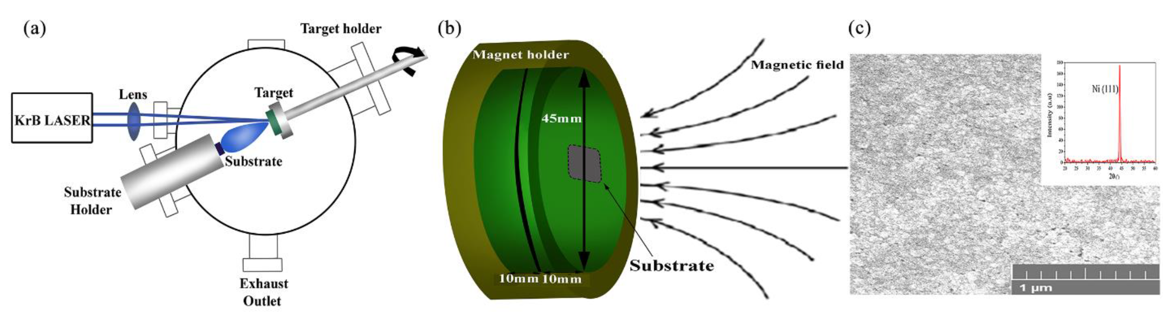
Figure 2.
Schematic of process flow for the TAM fabrication. (a) Deposition of 1.15-μm silicon oxide (SiO2) on top of the silicon substrate using PECVD, (b) deposition of Ti/TiN with a thickness of 60/30 nm using PVD, (c) deposition of Al/Si/Cu (98/1/1 wt. %) with a thickness of 4.0 μm is using PVD, (d) photoresist patterning and formation of predesigned tapered resist, (e) photoresist angel formation and Al/Si/Cu etching, and (f) photoresist removal.
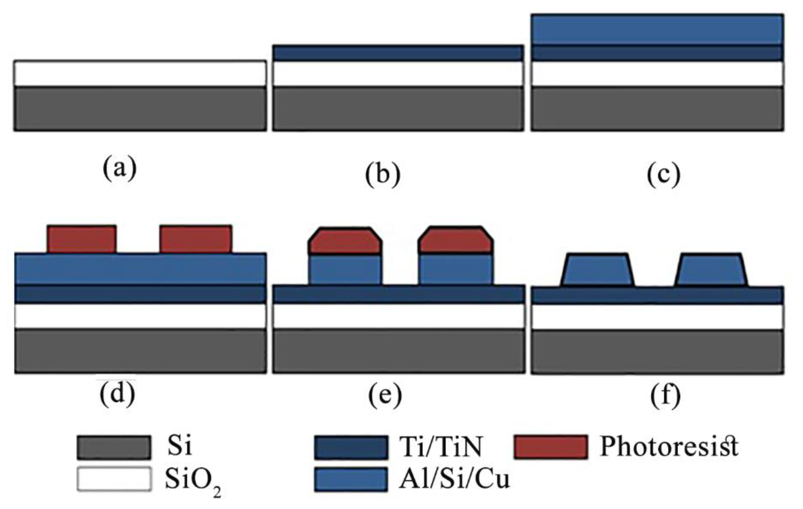
Figure 3.
Schematic of device design and experimental set up for measurement.
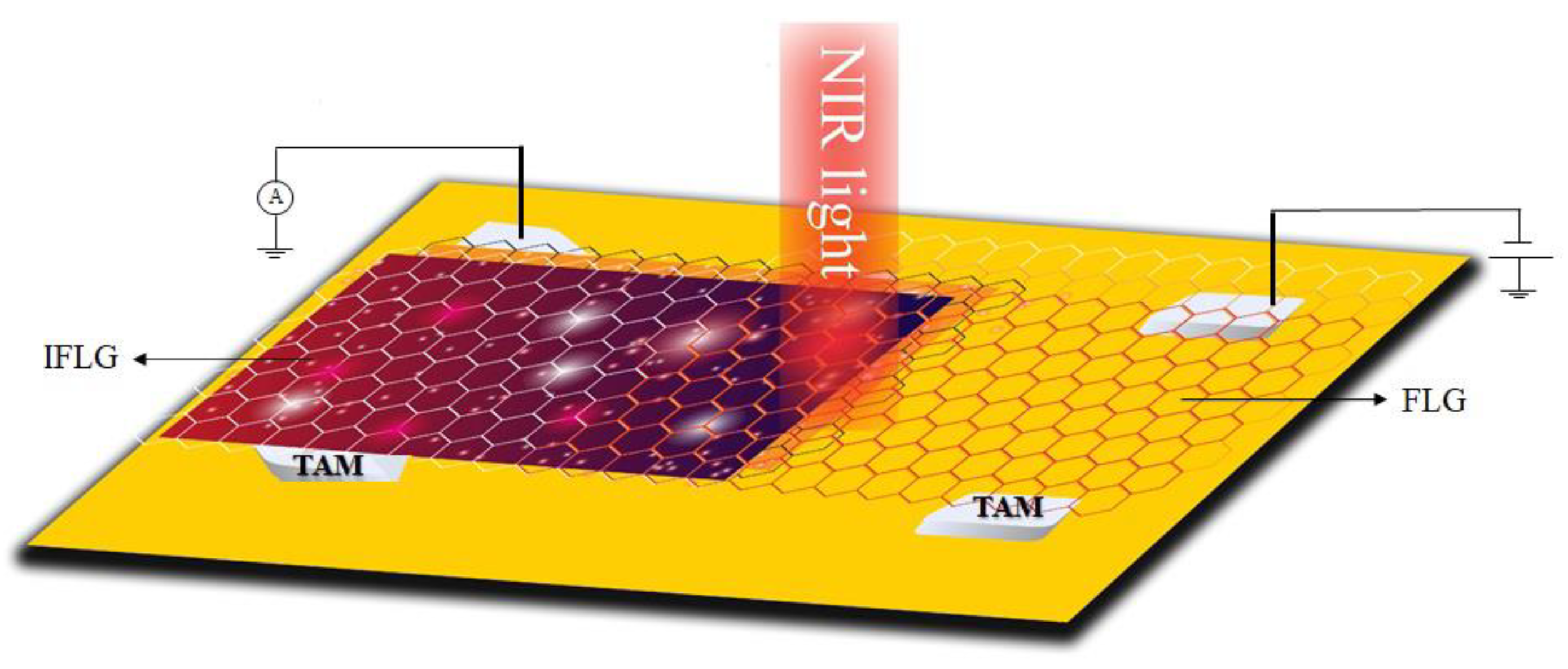
Figure 4.
Raman spectroscopy of MFPLD grown graphene under 350 mT magnetic field.
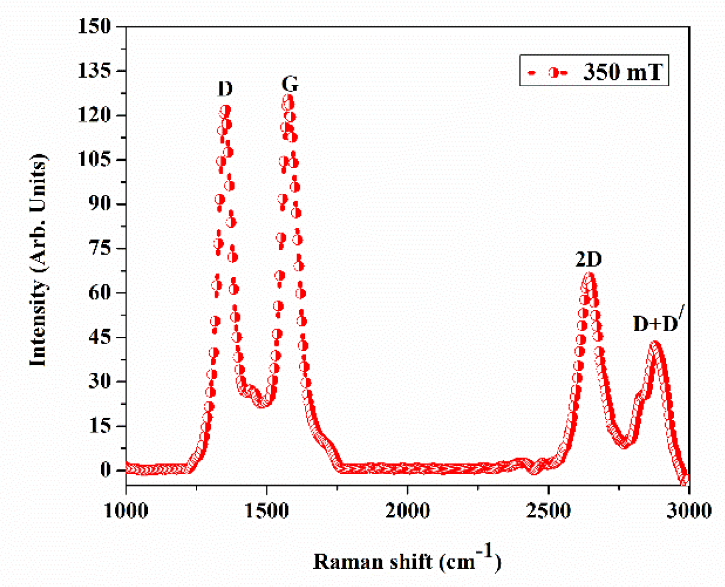
Figure 5.
ATR-FTIR spectrum of a of graphene grown by MFPLD under 350 mT magnetic field.
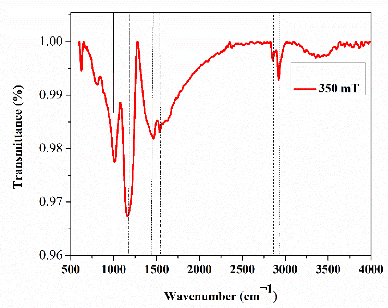
Figure 6.
Raman spectra of FLG and IFLG measured for 532 nm excitation: (a) low frequency region; (b) d G-band region, and (c) 2D-band region.
Figure 6.
Raman spectra of FLG and IFLG measured for 532 nm excitation: (a) low frequency region; (b) d G-band region, and (c) 2D-band region.
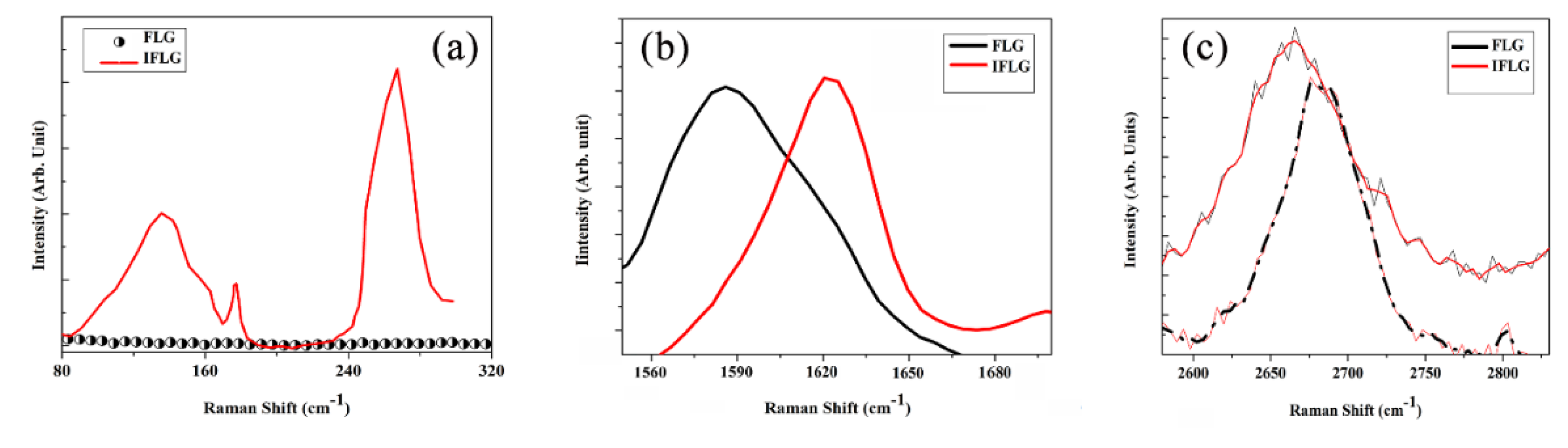
Figure 7.
Scanning Electron Microscope (SEM) image of (a) Tapered resist profile etch using resist plasma etching process (b) aluminium tapered microelectrode after aluminium etch process.
Figure 7.
Scanning Electron Microscope (SEM) image of (a) Tapered resist profile etch using resist plasma etching process (b) aluminium tapered microelectrode after aluminium etch process.
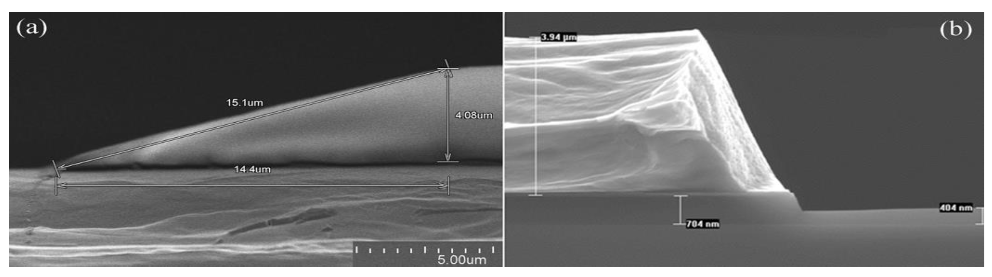
Figure 8.
(a) Responsivity and Quantum Efficiency (QE) spectra of the photodetector in NIR region at -0.5 negative bias voltages.
Figure 8.
(a) Responsivity and Quantum Efficiency (QE) spectra of the photodetector in NIR region at -0.5 negative bias voltages.
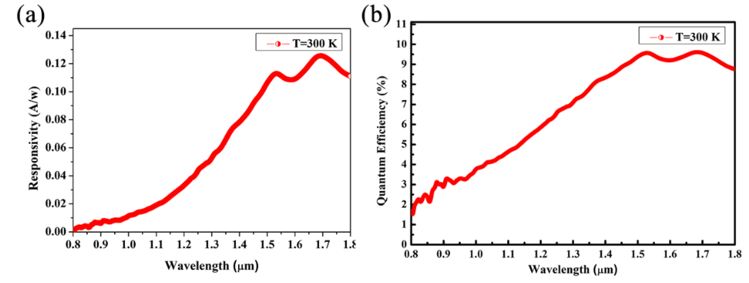
Figure 9.
Specific detectivity, (a) in NIR region at 300oK, and (b) at 176 THz (1.7 mm) vs temperature.
Figure 9.
Specific detectivity, (a) in NIR region at 300oK, and (b) at 176 THz (1.7 mm) vs temperature.
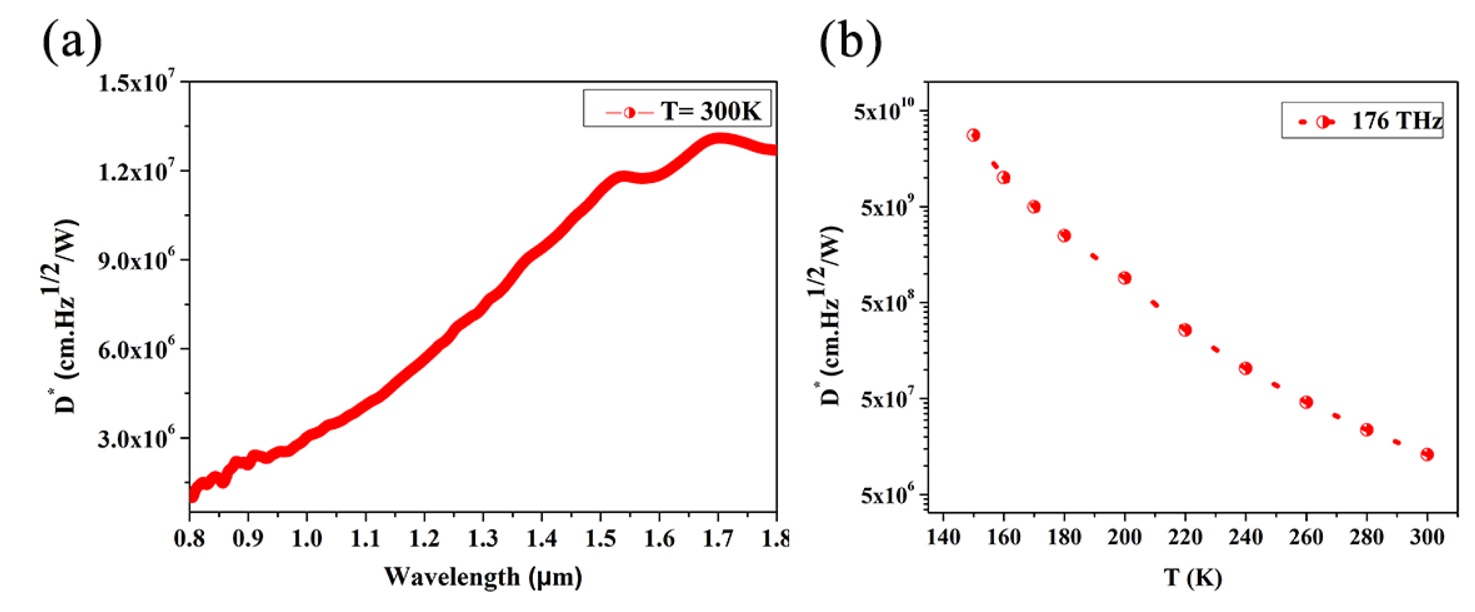

Table 1.
Raman peaks intensity and position for ID, IG, I2D, ID+D, ID/IG and I2D/IG of graphene grown by MFPLD under 350 mT magnetic field.
Table 1.
Raman peaks intensity and position for ID, IG, I2D, ID+D, ID/IG and I2D/IG of graphene grown by MFPLD under 350 mT magnetic field.
| Intensity | ID(a.u) | IG(a.u) | I2D(a.u) | ID+D’(a.u) | ID/IG | I2D/IG | |
|---|---|---|---|---|---|---|---|
| Growth | |||||||
| 350 mT magnet | 128 (1359) | 120 (1580) | 80(2645) | 44.5(2890) | 1.06 | 0.66 | |
Table 2.
Main ATR-FTIR peak position (PP) of graphene grown under 350 mT magnet.
| PP | 1010.65 | 1162.24 | 1464.32 | 1537.04 | 2856.03 | 2924.10 | 3356.78 |
Disclaimer/Publisher’s Note: The statements, opinions and data contained in all publications are solely those of the individual author(s) and contributor(s) and not of MDPI and/or the editor(s). MDPI and/or the editor(s) disclaim responsibility for any injury to people or property resulting from any ideas, methods, instructions or products referred to in the content. |
© 2025 by the authors. Licensee MDPI, Basel, Switzerland. This article is an open access article distributed under the terms and conditions of the Creative Commons Attribution (CC BY) license (http://creativecommons.org/licenses/by/4.0/).
Copyright: This open access article is published under a Creative Commons CC BY 4.0 license, which permit the free download, distribution, and reuse, provided that the author and preprint are cited in any reuse.


