Submitted:
07 February 2025
Posted:
07 February 2025
You are already at the latest version
Abstract
Continuous wave tunable klystron is a microwave amplifier widely used in satellite earth stations. This type of klystron has outstanding characteristics of high efficiency and long lifespan. This article proposes a design scheme of an electron optical system for Ku-band continuous wave tunable klystron. The klystron adopts a depressed collector to improve the overall efficiency of the device, and the collector area is cooled by forced air. The emission current density of the cathode and the temperature of the drift channel and collector in klystron during the rated operating condition directly affect the device lifespan. The distribution of electron trajectories is simulated using 2-D and 3-D electromagnetic calculation software, and a thermal analysis simulation of the klystron structure is conducted. A reliable klystron design scheme was obtained through the above process, and it is experimentally verified under the testing of a klystron sample tube. The DC electron beam transmission rate of the klystron exceeds 99%, and high-frequency output state beam transmission rate is above 97.5%. During the testing process, the klystron can maintain a stable working state. This study laid an important technical foundation for the development of Ku-band tunable klystrons.
Keywords:
tunable klystron
; depressed collector
; electron optical system
; thermal analysis
1. Introduction
Klystron is a vacuum electronic [1] microwave amplifier with a wide range of applications [2,3,4]. Among them, tunable klystron is a relatively special type of wideband klystron. Due to its continuously tunable cavity frequency, the klystron can be tuned to different frequency points for operation. This type of klystron is widely used in earth stations that transmit ground signals to satellites, and has outstanding characteristics of high power, high efficiency, and long lifespan [5]. CPI Corporation has developed related klystron products covering the C-band and Ku-band, with continuous wave output power in the kilowatt range and a maximum operating bandwidth of 800MHz for Ku band products [6,7]. In addition, the article [8] introduces a high peak power Ku-band tunable klystron.
This article proposes a design scheme for a 6-cavity klystron electron optical system [9] with a Ku-band operating bandwidth of 1.2 GHz. The electron trajectories were calculated using 2-D and 3-D software, and the simulation results show that the electron beam has a high transmission rate, which can meet the requirements of continuous wave output of the klystron. In order to ensure the lifespan and high efficiency of the klystron, thermal analysis [10,11,12] calculations on the relevant components of the klystron are carried out. The calculation results showed that the temperature distribution was within a reasonable range. In addition, the testing of the developed sample tube further verified that the design of the electron optical system can ensure the stable operation of the klystron.
2. Calculation of Basic Parameters
The main electrical property parameter of the Ku-band tunable klystron are listed as follows: output power of about 2.5 kW, electron gun perveance of about 1.15 μP, electron efficiency of beam wave interaction of about 24%, and working center frequency in the range of 14 GHz-15 GHz. The high-frequency structure of the entire tube adopts 6 tunable rectangular cavities. The basic structure of the optical system is shown in Figure 1.
According to the general design method of the klystron [13], based on the above parameters, it can be calculated that the cathode voltage of the klystron is -9.5 kV, the cathode emission current is 1.05 A, and the axial propagation constant of the electron beam is:
ω is the angular frequency of the electromagnetic wave, and v0 is the axial velocity of the electron beam. The radial propagation constant is:
Assuming the electron beam radius is b and γeb is around 0.8, the estimated electron beam radius is 0.53 mm. If the filling ratio of the electron beam is 70% of the drift channel, the drift channel radius is 0.75 mm.
Another important parameter of the electron optical system is the size of the focusing magnetic field. Firstly, the value of the Brillouin magnetic field can be obtained through current, voltage, and electron beam radius, where Bb is in Gs and b is in cm.
The magnetic field of this klystron adopts a partially restricted flow focusing method, and the working magnetic field B0 in the uniform magnetic field region is about 3400 Gs with a size of more than 2Bb.
According to the theory of space charge waves, the plasma angular frequency ωp is an important parameter for describing the electron beam bunching process and is an important basis for selecting the drift tube length between resonant cavities. For a drift tube of finite size, the plasma angular frequency ωq is relatively reduced compared to the case of an infinite electron beam, and the reduction ratio is represented by F. It is calculated as follows:
The corresponding plasma wavelength is:
When the distance between adjacent resonant cavities is 1/4 of the amendatory plasma wavelength, the maximum beam density modulation can be achieved, with a center distance of approximately 11 mm between cavity 1 and cavity 2. As the fundamental component of the beam current increases, the reduction of plasma frequency also increases, and the length of the drift tube needs to be correspondingly reduced. Taking into account the above factors, the optimization results of the beam wave interaction using 1-D software Kly based on large signal theory [14] show that the entire drift tube length formed by the six cavities is at least 42 mm. In the next section, the calculation of electron optical system will be based on a structure of 42 mm drift tube length and a 0.75 mm drift tube radius.
3. Simulation and Experimental Results
The following will describe the calculation results of the permanent magnet focusing magnetic field, electron trajectory in the electron gun region and the depressed collector region, and the thermal analysis of the tube body and depressed collector. Finally, based on this, the sample tube was tested.
3.1. Electrostatic Focusing Trajectory of the Electron Gun
Based on 2.5 D Arsenal-MSU [15], by optimizing the radius of the focusing electrode and the curvature radius of the cathode surface, the electron beam waist can be adjusted to the channel entrance position. To ensure the emission current of 1.05 A, the distance between the anode head and the cathode should be optimized. The adjusted electrostatic focusing electron trajectory of the electron gun is shown in Figure 2(a), and the radial distribution of emission current density on cathode surface is shown in Figure 2(b). From the figure, it can be seen that the current density at the cathode edge reaches the maximum value of 4.5 A/cm ² within the region. Low current density is suitable for klystron continuous wave operating conditions.
3.2. Electron Trajectories Under Permanent Magnet Focusing
In order to leave space for the tuning mechanism, the klystron adopts a C-shaped permanent magnet focusing structure as can be seen in Figure 3(a). The magnetic steel material is made of NdFeB.
To obtain a uniform magnetic field in the drift zone of the electron beam and a suitable magnetic field in the transition zone of the electron gun, the position of the electron gun pole shoes and the shape of the magnetic steel were simulated and optimized in CST [16]. The axial magnetic field distribution obtained is shown in the Figure 3(b). The maximum magnetic induction intensity on the axis region reaches 0.34 T. Under the condition of adding a focused magnetic field, the trajectories of electrons calculated in Arsenal for the entire tube are shown in Figure 4. As shown in the figure, the beam fluctuation is small, ensuring a high beam transmission rate.
In order to obtain an appropriate current distribution in the depressed collector [17,18,19] region, electron trajectories simulations are conducted under DC and high-frequency output states, respectively. To obtain the electron trajectory distribution in the depressed collector region under high-frequency output state, it is necessary to obtain the state parameters of electrons that have interacted with high-frequency field. In the PIC simulation model of the output cavity in Figure 5(a). In Figure 5(b), a 2-D cross-section near the inlet of the depressed collector can obtain parameters such as the velocities and charges of the electrons flow in the cross-section over a period of time.
The above data can be used as the electron source for the collection electrode in the particle trajectory simulation model. The following two figures show the electron trajectory distribution in the depressed collector region under DC and high-frequency states, respectively.
Figure 6.
(a) Electron trajectories diagram in DC state. (b) Electron trajectories diagram in high-frequency output state.
Figure 6.
(a) Electron trajectories diagram in DC state. (b) Electron trajectories diagram in high-frequency output state.
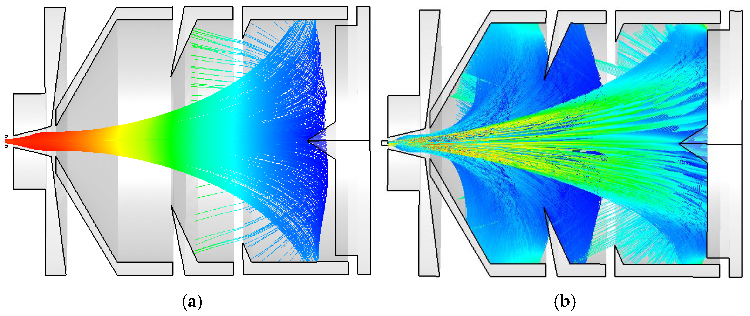
The collector voltage of each state remains constant. From the above figure, it can be seen that in the DC state, due to the electrons do not convert kinetic energy to the high-frequency field, most of the electrons hit the third collector surface. In the high-frequency output state, more low-energy electrons are intercepted by the front two collector poles, and high-energy electrons hit the rear two collector poles. The current and voltage of the depressed collector in the two states are shown in the Table 1.
3.3. Thermal Analysis of the Tube Body and Depressed Collector
To verify the feasibility of the structure, thermal analysis simulations with Ansys [20] were also conducted on the two main heating components, the tube body and the depressed collector. Both the collector and the tube body adopt forced air cooling for heat dissipation. Considering the actual situation, high-frequency interaction structures may intercept some electrons to form tube currents. Under the premise of a 97% electron transmission rate, the tube current will reach approximately 31mA and the heat dissipation power will be 295 W. In Ansys model, assuming that the heat source is uniformly dispersed inside the channel, and the temperature distribution of the channel under forced air cooling is shown in Figure 7. From the figure, it can be seen that the high temperature points of the tube are all located at the drift gap, with the highest temperature reaching 122 ℃. In actual, the interception location may be concentrated at a certain point within the channel, causing higher temperatures and even causing the drift head to melt and damage the klystron. The tube current below 30 mA is a necessary condition for continuous wave testing.
In addition, based on the distribution of collector current and voltage in high-frequency state obtained in section 3.2, the dissipated power of each collector can be calculated. Assuming Vk is the cathode voltage, Vc is the collector voltage, and Ic is the collector current, then the dissipated power of the collector is:
The collector temperature distribution obtained under the conditions calculated by equation (6) in the ANSYS model is shown in Figure 8. All collector poles are equipped with heat sinks, and the cooling air volume reaches 800 m³/h. It can be seen that the first collector pole, due to its high power, has a highest surface temperature of 435 ℃ in the entire region. The collector material is copper. In order to prevent excessive surface temperature, a molybdenum layer should be sputtered on the collector poles surface in the experimental sample tube.
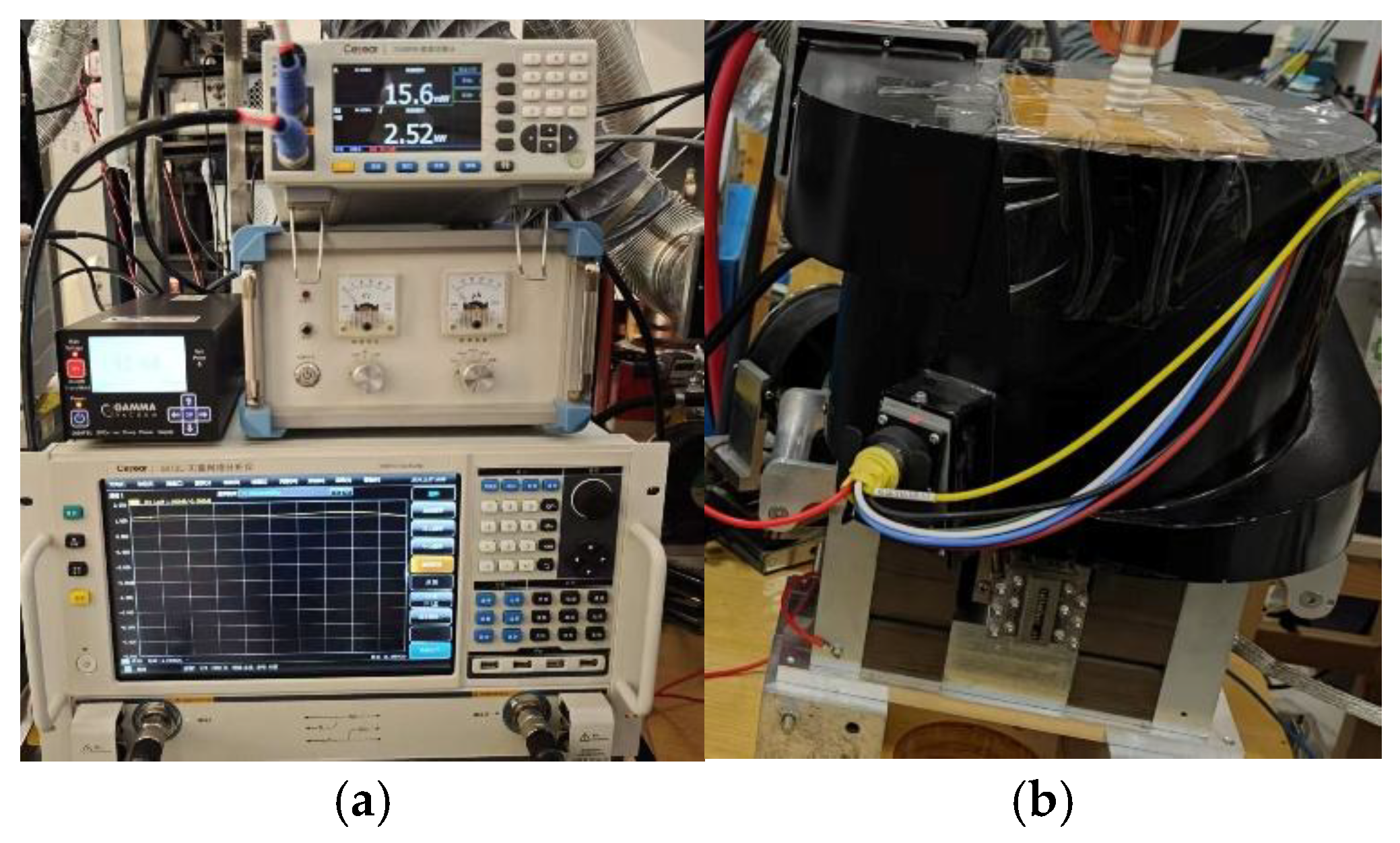
3.4. Testing of the Sample Tube
On the basis of the above simulation, the development and testing of sample tube are carried out.
Under the condition of -9.5 kV continuous wave cathode voltage, the total current of cathode emission reaches 1060 mA. The DC transmission rate of electron beam is over 99%, and the transmission rate in high-frequency output state is above 97.5%. The temperature of the outer wall of the tube body remains stable at around 60℃,The air temperature at the outlet of the collector fan do not exceed 60℃ when operating at rated power. The test results have well demonstrated the feasibility of the electron optical system.
Figure 9.
(a) Power testing of the sample tube. (b) Photo of the sample tube.
4. Discussion
In the high-frequency range, small size klystrons are often damaged due to deterioration of internal vacuum degree. One of the important reasons is the gas discharge caused by high temperature in the tube and the collector region. In this article, an electron optical system for Ku-band 6-cavity tunable klystron with depressed collector is proposed. The simulation results of particle trajectories indicate that the focused electron beam exhibits small fluctuations, a high transmission rate, and uniform current distribution within the collector region. The thermal analysis indicates that the primary heating components of the entire tube are within an appropriate temperature range. In the testing process, the electron transmission rate in DC state exceeds 99%, while the transmission rate in the high-frequency output state is above 97.5%. The klystron is capable of maintaining stable operation in a continuous wave output mode. In this simulation, the peak temperature within the collector region is observed at the surface of the first collector pole, which may lead to overheating. To alleviate the impact, potential structural modifications and surface treatments for the first collector pole will be further investigated.
Author Contributions
Conceptualization, X. Guo, B. Shen and H. H. Gu; methodology, X. Guo, Z. Q. Zhang, B. Shen and H. H. Gu; software, X. Guo, Y. Liang; validation, Z. Q. Zhang, H. B. Ding, and B. Shen; formal analysis, X. Guo; investigation, X. Guo; resources, X. Guo; data curation, X. Guo; writing—original draft preparation, X. Guo; writing—review and editing, X. Guo, Z. Q. Zhang, Y. Liang; visualization, X. Guo; supervision, H. B. Ding; project administration, Z. Q. Zhang, B. Shen, H. B. Ding. All authors have read and agreed to the published version of the manuscript.
Funding
This research received no external funding.
Data Availability Statement
Data are unavailable due to the requirements of confidentiality review by the research department of this study.
Conflicts of Interest
The authors declare no conflicts of interest.
References
- R.K. Parker, R.H. Abrams, B.G. Danly, and B. Levush, Vacuum Electronics. IEEE Trans. Microwave Theory Tech. 2002, vol. 50, no. 3, pp. 835-845. [CrossRef]
- A. Beunas, R. Marchesin, J. C. Bellemere, F. Kazarian, L. Delpech, M. Prou, C. Goletto, and E. Bertrand, High-Power CW Klystron for Fusion Experiments. IEEE Trans. Plasma Sci. 2009, vol. 56, no. 5, pp. 864-869. [CrossRef]
- A. Y. Baikov, C. Marrelli, and I. Syratchev, Toward High-Power Klystrons With RF Power Conversion Efficiency on the Order of 90%. IEEE Trans. Electron Devices. 2015, vol. 62, no. 10, pp. 3406-3412. [CrossRef]
- R. A. Cormier, and A. Mizuhara, 250 kW CW klystron amplifier for planetary radar. IEEE Trans. Microwave Theory Tech. 1992, vol. 40, no. 6, pp. 1056-1062. [CrossRef]
- H. Sato, M. Shintani, Y. Suzuki, T. Kageyama, T. Shinozaki, Y. Morizumi, and E. Watanabe. A 30 GHz, 500 W klystron amplifier for satellite earth stations. In IEDM, Washington, DC, USA, 05 Dec 1977. [CrossRef]
- T. Habermann, R. Begum, B. Stockwell, and L. Zitelli. Development of a tunable, air-cooled, all-gun PM-focused Ku-band klystron. In Third IVEC, Monterey, CA, USA, 25 Apr 2002. [CrossRef]
- Communications & Power Industries. Available online: https://www.cpii.com/product.cfm/4/13 (accessed on 05 Feb 2025).
- J. Page, A. Balkcum, R. Begum, L. Cox, T. Habermann, M. Henderson, T. Hunter, A. Staprans, B. Stockwell, and L. Zitelli. Design and Operation of a Pulsed 25 KW, MSDC Ku-Band Klystron. In 2010 IVEC, Monterey, CA, USA, 18 May 2010. [CrossRef]
- R. Zhang, Y. Wang, H. P. Han, and J. X. Xie. Electron Optics System of a 100-MW S-Band Klystron. IEEE Trans. Electron Devices. 2010, vol. 57, no. 5, pp. 1146-1151. [CrossRef]
- A. K. Bandyopadhyay, A. Nagaraju, R. Guha, R. K. Sharma, and D. Pal. Thermal simulation of a Multiple Beam Electron gun for Ku-Band Klystron. In 2019 IVEC, Busan, South Korea, 01 May 2019. 01 May. [CrossRef]
- L. K. Behnke, K. L. Montgomery, D. R. Whaley, R. B. True. Electron Gun Thermal Design, Analysis and Experimental Validation. In 2006 IVEC, Monterey, CA, USA, 25 Apr 2006. [CrossRef]
- A. V. Konnov, A. P. Nikitin, P. I. Akimov, V. I. Ppanizkov, I. S. Vladykina. Thermal analysis of multibeam klystron collector with forced air cooling. In 2014 IVESC, St. Petersburg, Russia, 04 Jul 2014. [CrossRef]
- Y. G. Ding. General design of klystron. In Book Design, Manufacture and Application of High Power Klystron, 1st ed.; Editor 1, B. S., Editor 2, D. P. Gao; National Defense Industry Press: Beijing, China, 2010; Volume 3, pp. 49–61.
- T. Kageyama, Y. Morizumi, and E. Watanabe. A large-signal analysis of broad-band klystrons with design applications. IEEE Trans. Electron Devices, 1977, vol. 24, no. 1, pp. 3-12. [CrossRef]
- Y. G. Ding, X. H. Xiao, V. E. Rodiakin, and A. N. Sandalov. Theoretical and experimental investigations of the high power MBK, based on 2.5 D Arsenal-MSU computer code. In ICMMT 2000, Beijing, China, 14 Sep 2000. [CrossRef]
- CST Studio Suite. Available online: https://www.3ds.com/products/simulia/cst-studio-suite (accessed on 5 February 2025).
- H. G. Kosmahl. Modern multistage depressed collectors—A review. Proc. IEEE. 1982, vol. 70, no. 11, pp. 1325-1334. [CrossRef]
- A. M. Latha, R. K. Sharma, Y. Kumar, and S. K. Ghosh. Techniques for the Development of Multistage Depressed Collectors. IEEE Trans. Electron Devices. 2015, vol. 62, no. 6, pp. 2038-2043. 2038; 62. [CrossRef]
- X. He, Y. M. Zhang, S. W. Feng, W. J. Yu, and M. P. Yang. A New Method for Measuring Thermal Characteristics of Multistage Depressed Collectors. IEEE Trans. Electron Devices. 2019, vol. 66, no. 12, pp. 5404-5406. [CrossRef]
- Ansys Software. Available online: https://www.ansys.com/ (accessed on 5 February 2025).
Figure 1.
Schematic diagram of klystron optical system structure.
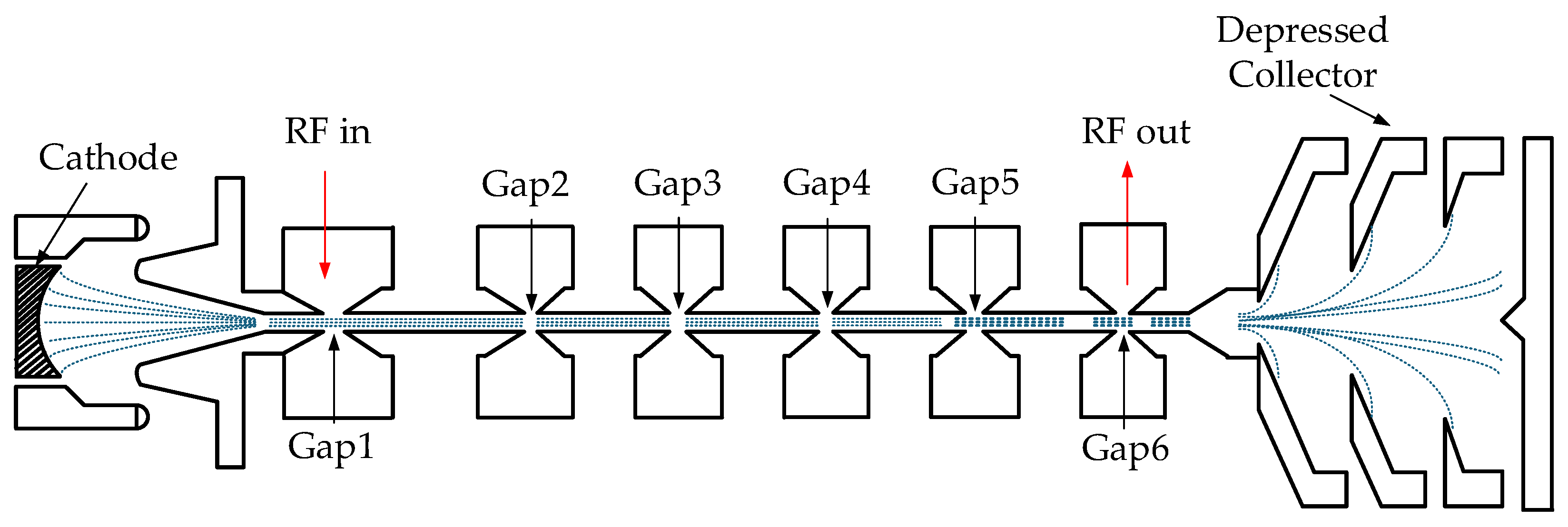
Figure 2.
Simulation results of electrostatic focusing of the electron gun. (a) Electron trajectories; (b) Radial distribution of current density on cathode surface.
Figure 2.
Simulation results of electrostatic focusing of the electron gun. (a) Electron trajectories; (b) Radial distribution of current density on cathode surface.
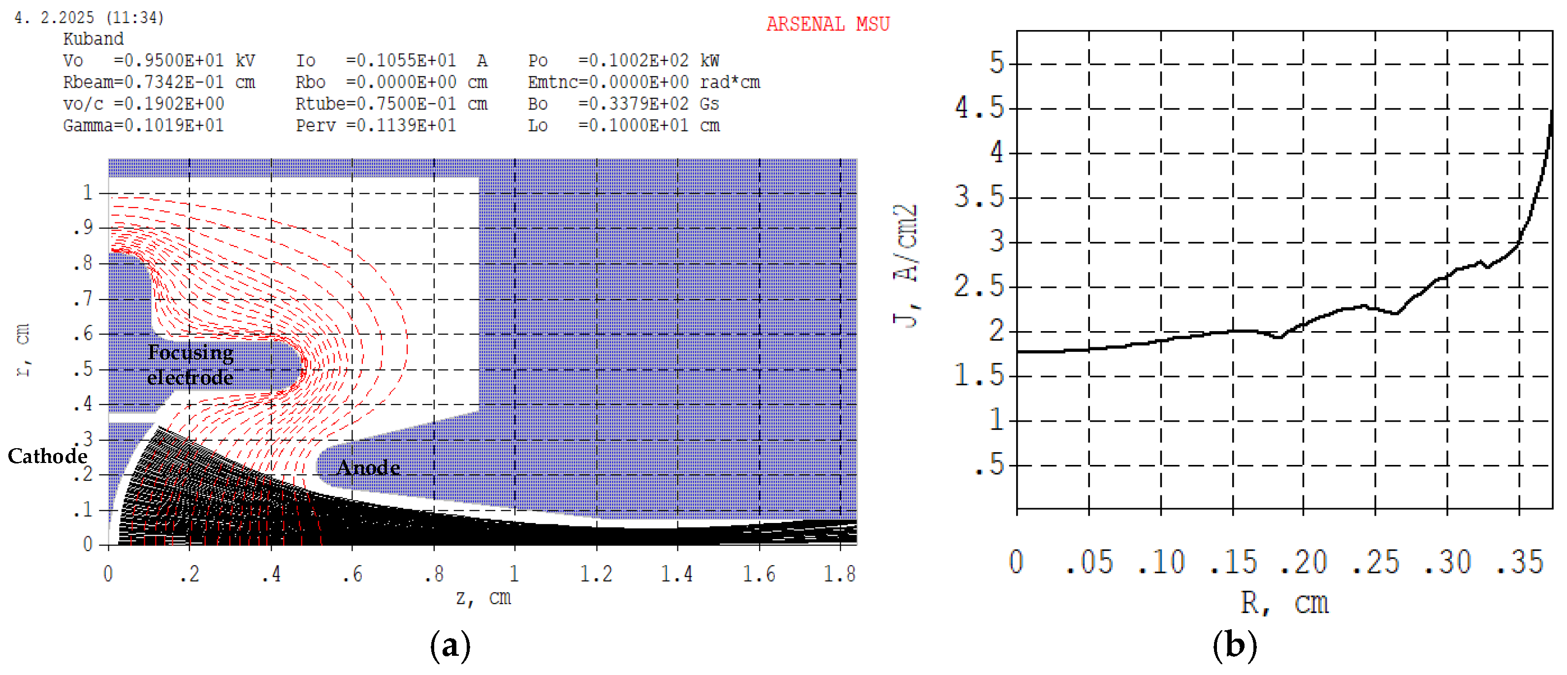
Figure 3.
The permanent magnet focusing system. (a) Permanent magnet structure; (b) Axial magnetic field distribution.
Figure 3.
The permanent magnet focusing system. (a) Permanent magnet structure; (b) Axial magnetic field distribution.
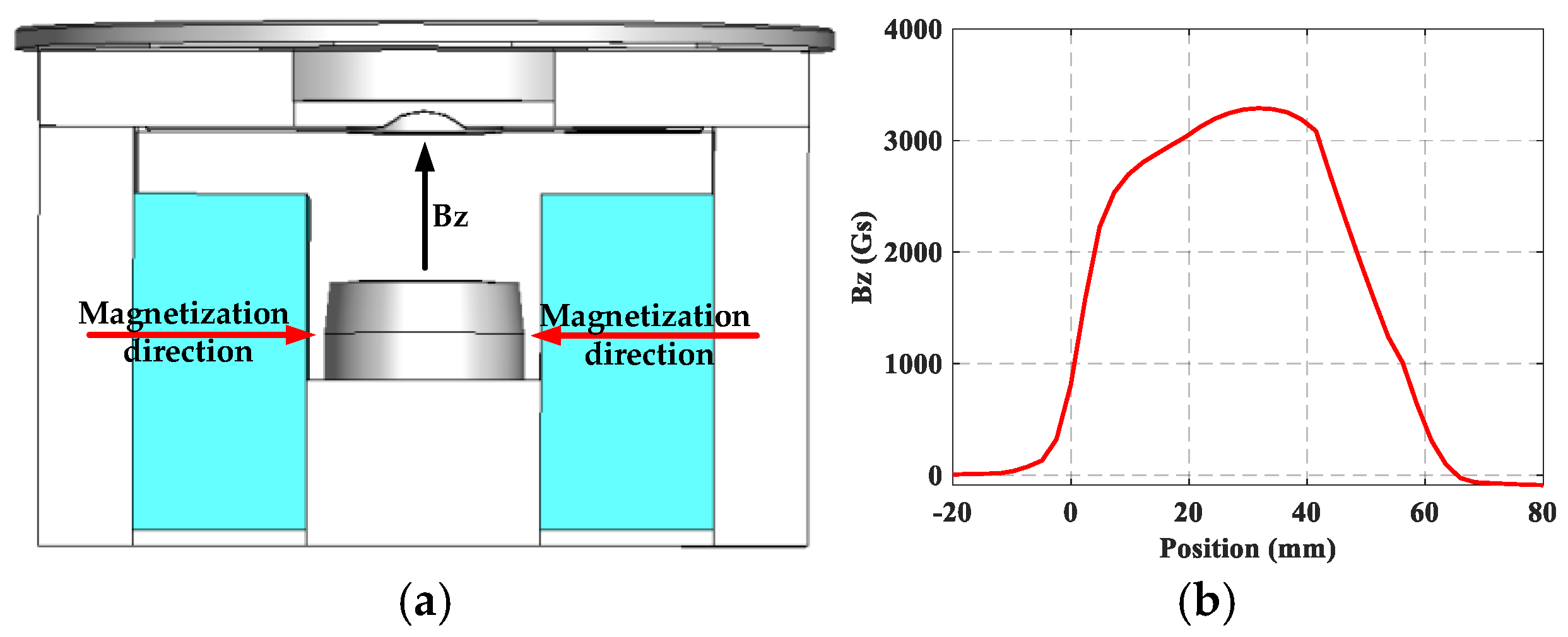
Figure 4.
Electron trajectories of the entire tube simulated in Arsenal.
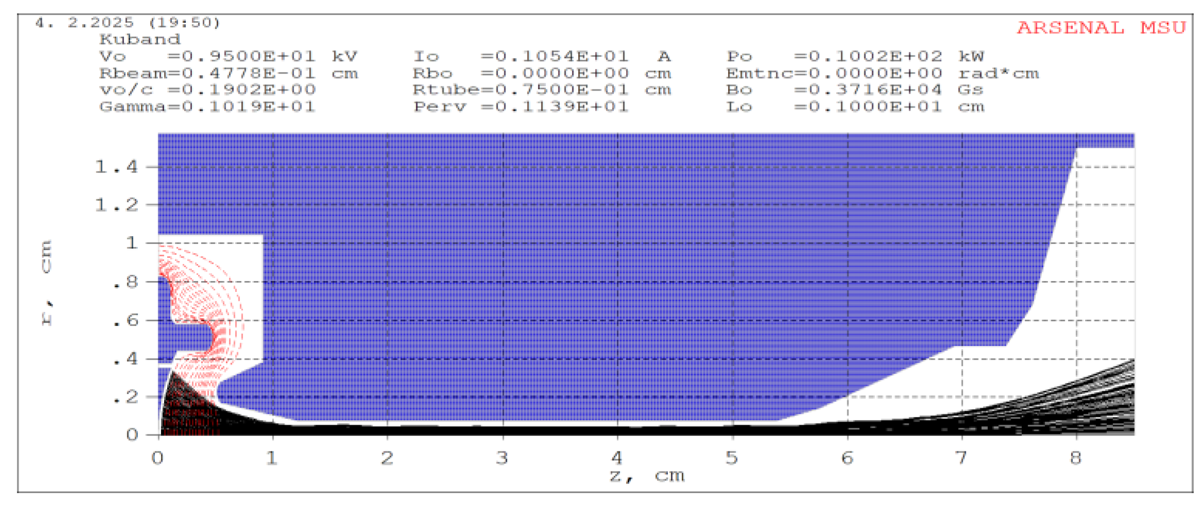
Figure 5.
(a) Electron bunches diagram in the output cavity.(b) Electrons in 2-D cross-section near the inlet of the depressed collector.
Figure 5.
(a) Electron bunches diagram in the output cavity.(b) Electrons in 2-D cross-section near the inlet of the depressed collector.
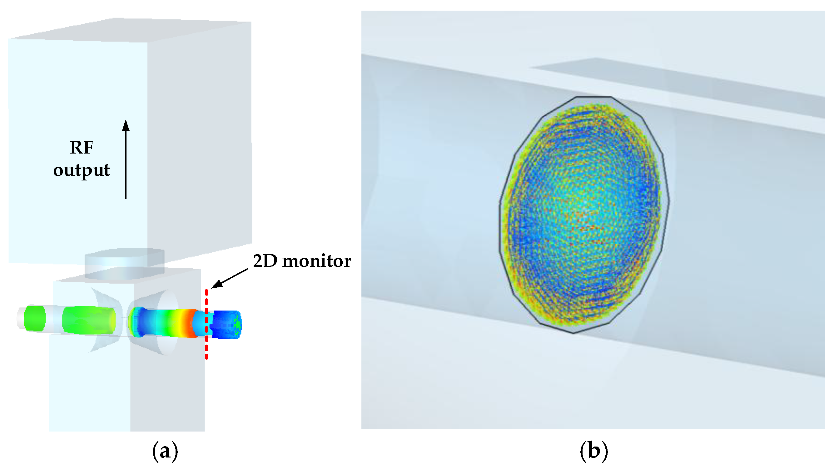
Figure 7.
Temperature distribution inside the tube body.
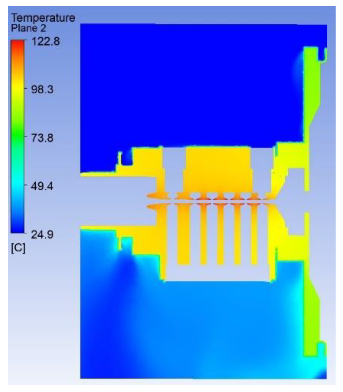
Figure 8.
Temperature distribution inside the depressed collector.
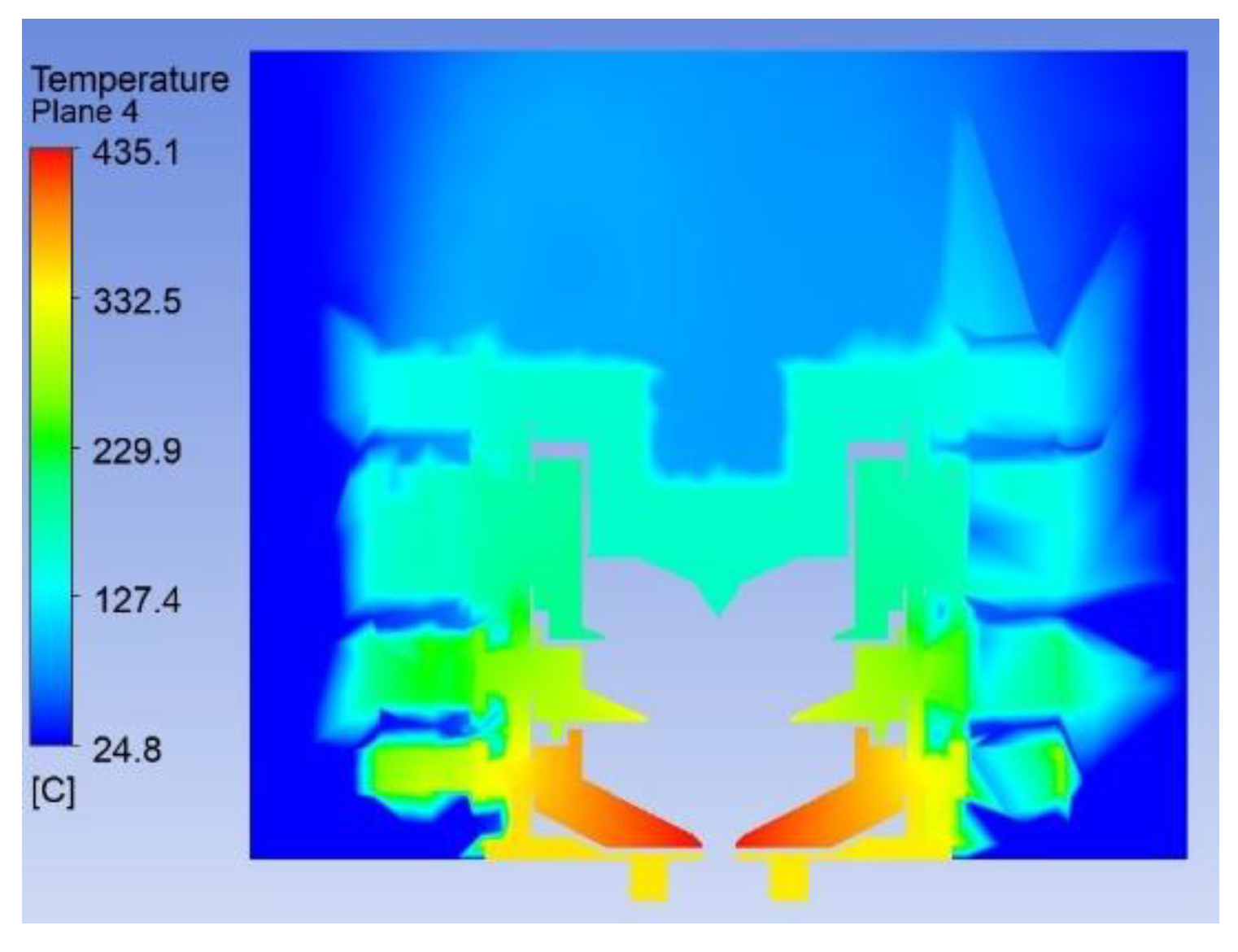

Table 1.
Collector parameters under DC and high-frequency output states.
| Title 1 | DC state | High-Frequency state |
| 1st collector voltage | 0 kV | 0 kV |
| 2nd collector voltage | -4 kV | -4 kV |
| 3rd collector voltage | -7.5 kV | -7.5 kV |
| 4th collector voltage | -9.5 kV | -9.5 kV |
| 1st collector current | 120 mA | 420 mA |
| 2nd collector current | 210 mA | 255 mA |
| 3rd collector current | 690 mA | 225 mA |
| 4th collector current | 30 mA | 150 mA |
Disclaimer/Publisher’s Note: The statements, opinions and data contained in all publications are solely those of the individual author(s) and contributor(s) and not of MDPI and/or the editor(s). MDPI and/or the editor(s) disclaim responsibility for any injury to people or property resulting from any ideas, methods, instructions or products referred to in the content. |
© 2025 by the authors. Licensee MDPI, Basel, Switzerland. This article is an open access article distributed under the terms and conditions of the Creative Commons Attribution (CC BY) license (http://creativecommons.org/licenses/by/4.0/).
Copyright: This open access article is published under a Creative Commons CC BY 4.0 license, which permit the free download, distribution, and reuse, provided that the author and preprint are cited in any reuse.


