Submitted:
26 January 2025
Posted:
28 January 2025
You are already at the latest version
Abstract
The article proposes a synchronous step-down converter implemented with P-channel and N-channel transistors. The transistors are controlled by a single driver, and “dead time” is implemented with external circuits. When an initial problem occurs with ensuring this time in practical implementation, the influence of the Schottky diode capacitance on “dead time” is considered. Mathematical expressions were derived, showing the ratio of the value of this capacitance and the input capacitance of the transistor, and the influence of this ratio on the shape of the leading edge of the pulse for switching on the transistor. Results of computer simulation are given for different ratios of the two capacitances. The results of the mathematical description and computer simulation were used to select a suitable transistor and Schottky diode and are applied in the subsequent practical implementation. Conclusions and recommendations were done, for the synchronous step-down converter, as well as for other cases of implementing dead time in the manner considered.
Keywords:
synchronous step-down converter
; dead time
; P-channel MOSFET
; N-channel MOSFET
; Schottky diode
; junction capacitance
1. Introduction
The main issues in the design of DC/DC converters are presented in [1]. The difference between continuous and discontinuous current mode through the inductance is discussed for example in [2]. Typically, the synchronous step-down converter is implemented with two N-channel MOSFETs [3]. Issues related to the efficiency of such a converter are considered, for example, in [4,5,6,7]. The requirements for controlling MOSFETs are considered in many scientific works, such as [8,9,10,11,12,13]. In cases where the supply voltage does not exceed the maximum allowable gate-source voltage of a P-channel MOSFET, the upper N-channel transistor in the synchronous buck converter can be replaced by a P-channel transistor. This provides certain advantages in terms of controlling both transistors. It can be implemented by a single driver with push-pull output as shown in Figure 1. In this way, some additional elements are avoided to provide the control voltage of the upper transistor in case it is also N-channel – capacitor, diode and additional circuits [14]. However, it should be noted that in the proposed control in Figure 1, one of the two transistors is always on, while in the case of two N-channel transistors, both can be turned off under certain circumstances. This is a known disadvantage of the variant considered in this study, which is suitable, for example, when charging low-power energy storage elements - batteries, ultracapacitors. In this case, the constant current regulation and voltage limitation can be carried out, and when the maximum charging voltage is reached, the electronic regulator for this voltage remains to work, i.e. both transistors can be switched. Issues related to regulation and the rest of the control system are not the subject of consideration in this research. The charging circuits of the input capacitances of the two transistors is presented on Figure 1 (red lines) and the discharge circuits (blue lines). The additional elements to the gates of the transistors (the two resistors and the Schottky diode) are known and often recommended. Through these circuits, the so-called “dead time” is implemented when controlling the transistors. The goal is to turn one transistor on with a certain delay compared to turning the other off. This problem is known and also exists in other converters using phase leg transistors [15]. Different methods for realization “dead time” are known [16,17,18,19,20]. For the circuit of a synchronous converter using two N-channel MOSFETs, controllers in an integrated circuit are proposed, containing different methods for “dead time” realization [21,22]. The present work focuses on the realization with the circuits shown in Figure 1. The operating principle is as follows:
At a low level at the driver output (the lower transistor at its output is turned on), the input capacitance of the lower N-channel transistor is discharged through the diode and the driver output. At the same time, the input capacitance of the upper P-channel transistor is charged through the resistor to a voltage approximately equal to the supply +U (the difference is due to the voltage on the transistor at the driver output). At a high level at the driver output (the upper transistor at its output is turned on), the input capacitance of the upper P-channel transistor is discharged through the diode and the driver output. At the same time, the input capacitance of the lower N-channel transistor is charged through the resistor to a voltage approximately equal to the supply +U (the difference is due to the voltage on the transistor at the driver output). Since the charging of the input capacitances occurs through a resistor, the idea is to change its value and the charging time constant to change the turn-on delay time. It can be larger than that during turn-off, because the capacitance discharge occurs through the low-resistance Schottky diode [23].
In the literature known to the authors no methodology for sizing these circuits is described, especially with regard to the problem described below. This problem may occur in low-power converters, where the input power sources are small photovoltaics, piezoelectric elements, etc. In these cases, the transistors used are low-power. Characteristic features of low-power MOSFETs are the low threshold voltage (usually 0.7 – 1.5V) and the small value of the input capacitance (usually tens to hundreds of pF). When controlling power MOSFETs, the described problem could not arise, since their threshold voltage is high (usually above 4.5V), and their input capacitance is larger (up to several tens of nF).
Description of the problem: When controlling the transistors in the manner shown in Figure 1, the authors observed the oscillograms shown in Figure 2 and Figure 3. The supply voltage of the converter is 3.3V. In Figure 2 - CH2, a steep trailing front is observed in the voltage of the drains of both transistors (point A – Figure 1), i.e. the lower transistor turns on very quickly. At the same moment, a sharp decrease is observed in the supply voltage on CH1. These are signs of simultaneous conduction of both transistors, i.e. a single-arm short circuit. From CH1 in Figure 3, it can be seen that at the same moment in time, the gate-source voltage of the lower transistor increases steeply, and it has been established that the rate of increase is not affected by a change in the value of the resistor R1 from Figure 1. This prompted a more detailed study of these circuits, described below.
2. Mathematical Descriptions and Study
Essential to the solution of the described question is the consideration of the influence of the Schottky diode capacitance when applying a signal to turn on the transistor. The study was carried out using the circuit shown in Figure 4, where the Schottky diode capacitance and the input capacitance of the transistor are added to the elements existing in Figure 1. The equivalent circuit for mathematical description is presented in Figure 5.
It is assumed that the input voltage is increased stepwise to a value of 1 (single input pulse) and the change in the output voltage , which is the gate-source voltage of the transistor, is examined.
The expressions for the impedances from the circuit on Figure 5 in operator form are:
For a single input, the output voltage has the form:
It can be represented also:
where,
When switching from Laplace form to the original, the change in output voltage over time is obtained:
Figure 5 presents the two terms of expression (5) – the first with a blue line, the second – with a green line, and their sum – with a red line.
From Figure 6 it can be seen that the output voltage , which is the gate-source voltage of the transistor, has a sharp increase at the initial moment, which depends on the ratio of the two capacitances (the capacitance of the Schottky diode) and (the input capacitance of the MOSFET). For example, if the value of the initial increase will be of a negligible value. If the two capacitances are equal, this value will be equal to half the value of the input voltage. However, if, the initial increase may be close to the value of the input voltage. This is the effect that is observed in the upper oscillogram of Figure 3. The problem is that depending on the ratio of the two capacitances, the value of the initial increase may be greater than the value of the threshold voltage of the transistor. In such a situation, “dead time” is not realized and the effect described in the introduction is observed.
Formula (5) can be used to determine the value of the “dead time” depending on the value of the resistor at known other values. For this purpose, it is presented in the form:
When replacing and the expression is obtained:
By substituting in (7) the quantities from formula (4) we get:
Because dependencies were derived at unit input, then the value of should be set in units relative to the maximum value of the driver's output voltage. So, for example, if it is 3V and the threshold voltage is 1.8V, in formula (8) for value 0.6 should be substituted.
In formula (8), the capacitance values are known from the reference data for the selected elements – Schottky diode, MOSFET and Zener diode parallel to the gate-source transition. The value of resistor is usually 10K. It remains for different values of to calculate the value of and choose the appropriate value of the resistor.
So, for example, for variant 4 of table 1 considered below, the values are as follows: ; ; . With a minimum threshold voltage of 1V for the MOSFET and an output voltage from the driver of 3V in formula (8) is placed . After calculation at resistor value a value is obtained for 111 ns.
A computer simulation was performed using models of real diodes and transistors. The results are shown and commented below.
Variant 1 – Schottky diode 1N5819 with a capacitance of 150 pF [24], input capacitance of the transistor 150 pF. The input signal has a maximum value of 5V. The simulation scheme and the results are shown on Figure 7.
It can be seen that when a signal is applied to turn on, the initial peak of the output voltage is 2.5 V in accordance with the coefficient A from Figure 6. When switched off, an initial retention of about 0.3 V (the voltage across the switched-on Schottky diode) is observed. It is clear that with such a combination, the realization of dead time will not be obtained for transistors with a threshold voltage below 2.5 V.
Variant 2 - Schottky diode 1N5819 with a capacitance of 150 pF [24], input capacitance of the transistor 500 pF. The input signal has a maximum value of 5V. The simulation scheme and the results are shown on Figure 8.
It can be seen, when a signal is applied to turn on, the initial peak of the output voltage is approximately 1V in accordance with the coefficient A from Figure 6. When switched off, an initial retention of about 0.3 V (the voltage across the switched-on Schottky diode) is observed. It is clear that with such a combination, the realization of “dead time” will not be obtained for transistors with a threshold voltage below 1V. When the input capacitance of the transistor increases, the initial jump of the gate-source voltage decreases.
Variant 3 – Silicon diode 1N4148 with a capacitance of 3 pF [25], input capacitance of the transistor 500 pF. The input signal has a maximum value of 5V. The simulation scheme and the results are presented on Figure 9. This option was chosen because pulse diodes with a PN junction are characterized by significantly smaller capacitance values.
This variant corresponds to the condition It can be seen that when a signal is applied to turn on, the initial peak of the output voltage is negligibly small in accordance with the coefficient A - Figure 6. It is clear that with such a combination the implementation of “dead time” when turning on the lower transistor will be the easiest even at low threshold voltages. When turning off, an initial hold of a value of about 0.7 V (the voltage on the switched-on diode) is observed. However, this is unpleasant, since at the same moment a signal is applied to turn on the upper transistor of the synchronous converter and at threshold voltages of the lower one about 0.7 V the latter may remain on for a short time. This would make it difficult to implement “dead time” when turning on the upper transistor. For this reason, the authors recommend using Schottky diodes, as in the scheme on Figure 1.
Variant 4 – Connecting a zener diode in parallel with the gate-source junction of the transistor. The diode has protective functions and are described in the literature [8,9]. The schematic diagram together with the capacitances is shown on Figure 10. - Schottky diode 1N5819 with a capacitance of 150 pF [24], input capacitance of the transistor 500 pF, zener diode BZX84C5V6 SMD with a capacitance of 200 pF [26]. The input signal has a maximum value of 5V. The simulation scheme and the results are shown on Figure 11.
This variant differs from variant 2 only in the inclusion of the zener diode. From the comparison of the timing diagrams on Figure 11 with those on Figure 8, it is seen that the initial peak is reduced to about 0.9 V, which would facilitate the implementation of “dead time” for transistors with a threshold voltage above 1V. In addition to the protective function, the authors recommend placing a zener diode also from the point of view of the issue considered in this article.
3. Experimental
The initially implemented variant for the lower transistor on Figure 1 is the following: transistor BSS214N with capacitance and threshold voltage [27] and Schottky diode SS34 with capacitance [28]. The oscillograms shown on Figure 2 and Figure 3 correspond to this variant. From the previous consideration, it is clear that this variant is unsuitable. Table 1 shows various possible variants for implementation - combinations of Schottky diodes and transistors with or without a zener diode. Those shown in red are unsuitable, the one in yellow is not preferable, since the results are close to the limit. From the point of view of “dead time”, variants 4, 5 and 6 are suitable - shown in green. Variants 5 and 6 are not preferred due to the considerations expressed when commenting on the results in Figure 9. The preferred implementation variant is 4, shown in blue in the first column of Table 1. It uses a Schottky diode SS14 with a significantly smaller capacitance than SS34 [29].
The last three variants from Table 1 were evaluated from the following point of view: When turning on the upper transistor from Figure 1 and increasing the voltage in point A, through the feedback capacitance of the lower transistor, its gate-source capacitance is charged (Miller effect) [30]. Shortly before this (to ensure the “dead time”) there is a low level at the driver output. In this situation, due to the feedback, the input capacitance would be charged to a voltage equal to the sum of the drop on the Schottky diode (or the pulse diode with a PN junction) and the voltage on the lower transistor of the driver. This sum of voltages must remain less than the threshold voltage of the lower transistor, otherwise it is possible to turn it on as well. With a sharp increase in the voltage at point A, the consideration made in the previous part can be applied. The results from Table 2 show that from such a point of view, variants 5 and 6 are borderline (shown in yellow). Variant 4 (in green) is also suitable for this consideration.
After the implementation assessment, variant 4 was chosen, and the part of the board corresponding to the scheme under consideration is shown in Figure 12. All electronic elements correspond to this variant 4.
Schottky diodes and are SS14 and correspond to and in Figure 1. Resistors and consist of two parallel-connected resistors with a value of 1K and correspond to and in Figure 1. Resistors and have a value of 10K and correspond to and in Figure 1. zener diodes BZM55C5V1 are soldered to these resistors. The transistor M1 (P-channel) is BSP250. The transistor M2 (N-channel) is UT6402G. The two drains pins are connected externally together with the left terminal of the inductance in the diagram of Figure 1 (point A – Figure 1).
Figure 13 and Figure 14 show the recorded oscillograms. The operating frequency of the converter is 17 kHz, and the supply voltage is 3.3 V.
From CN2 on Figure 13, the gradual increase in the gate-emitter voltage of the N-channel transistor when turned on (to realize “dead time” when turning off the P-channel transistor) and a rapid decrease (to realize “dead time” when turning on the P-channel transistor) are observed.
From CN2 in Figure 14, it can be seen that there are no short-term dips in the supply voltage both during switching on and during switching off of the N-channel transistor. The measured current, consumed by the power source in this case is significantly less than that in the case of Figure 2. These are proofs of correct implementation of dead time according to the scheme of Figure 10 for the two transistors of the synchronous step-down converter.
4. Conclusions
The article presents the results of the study of a synchronous step-down converter implemented with P-channel and N-channel MOSFET. The realization of “dead time” with external elements when controlled by a driver with push-pull output is considered. Main attention is paid to the influence of the Schottky diode capacitance. The main conclusions are as follows:
- It is recommended to implement the external circuits to the gate of the transistor according to the scheme in Figure 10.
- When designing “dead time’ circuits, it is necessary that the Schottky diode capacitance be significantly smaller than the input capacitance of the transistor.
- Based on formula (5) and Figure 6, the compliance with the threshold voltage of the MOSFET must also be checked.
- It is not recommended to use a pulse diode with a PN junction instead of a Schottky diode due to possible parasitic charging of the input capacitance of the transistor through the feedback capacitance when the upper transistor is turned off and possible reaching the threshold voltage of the lower.
- It is recommended to include zener diodes in parallel with the gate-source junction of the transistors with the lowest possible reference voltage, but greater than the maximum threshold (zener diodes with lower reference voltage have greater capacitance). In addition to their protective function, these diodes also facilitate the realization of “dead time”.
- Formula (8) can be used to determine the value of the dead time at different values of the resistor and known values of the other quantities as described above.
Acknowledgments
The authors express their gratitude to the rector and management of the University of Chemical Technology and Metallurgy, Sofia, Bulgaria for the financial support in publishing this article.
Conflicts of Interest
The authors declare no conflicts of interest.
References
- Jaunay, S.; Broun, J. DC-to-DC Design Guide, Vishay Siliconix, Application note AN607, Document number 71917, 10 Oct 2002. https://www.vishay.com/docs/71917/71917.pdf.
- Hudson, T. The Difference between CCM and DCM Explained, Monolithic Power System, Article #A-0022 Rev. 1.0, 5/27/2022.
- Maxim Integrated. Synchronous Rectification Aids Low-Voltage Power Supplies, Application note 652, Jan 31, 2001. https://www.maximintegrated.com/an652.
- Rohm Co. Efficiency of Buck converter, Application note No. 64AN035E Rev.004. November 2022.
- Raj, A. Calculating efficiency, Texas Instruments Application report SLVA390A-February 2010- Revised March 2020.
- He, X.; Li, D.; Zhang, V. An Accurate Approach for Calculating Efficiency of a Synchronous Buck Converter Using the MOSFET Plateau Voltage, Texas Instruments Application report SLVAEQ9-July 2020.
- Klein, J. “Shoot-through”in Synchronous Buck Converter, Fairchild, Application note AN-6003, 04/25/2003, www.fairchildsemi.com.
- Rohm, Co. , Basics and Design Guidelines for Gate Drive Circuits, Application note, No.66AN032E Rev.003, 2023.11.
- Toshiba, MOSFET Gate Drive Circuit, Application note, 2018-07-26.
- Green, P.B.; Zheng, L. Gate drive for power MOSFET in switching applications. A guide for device characteristics and gate drive techniques, Infineon Application note, AN 2203 PL18 2204 004502, V1.0 2022-04-20.
- Texas Instruments, Fundamentals of MOSFET and IGBT Gate Drive Circuits, Application Report, SLUA618A-March2017-RevisedOctober2018.
- On Semiconductor, Drive and Layout Requirements for Fast Switching High Voltage MOSFETs. https://www.onsemi.co/pub/collateral/tnd6242.pdf.
- On Semiconductor, Drive and Layout Requirements for Fast Switching High Voltage MOSFETs. https://www.onsemi.co/pub/collateral/tnd6242.pdf.
- Fairchild, Design and Application Guide of Bootstrap Circuit for High-Voltage Gate-Drive IC, Application note, AN-6076, 2008, Rev. 1.4*12/18/14. https://www.onsemi.jppub/collateral/an-6076jp.
- Ji, Y.; Yang, Y.; Zhou, J.; Ding, H.; Guo, X.; Padmanaban, S. Control strategies of mitigating dead-time effect on power converters: An overview. Electronics (Switzerland), 8(2), 2019, Article 196. [CrossRef]
- Zhen, S.; Zhang, B.; Luo, P.; Yang, K.; Zhu, X.; Li, J. A high efficiency synchronous buck converter with adaptive dead time control for dynamic voltage scaling applications, 2011 IEEE/IFIP 19th International Conference on VLSI and System-on-Chip, Hong Kong, 2011, pp. 43-48. [CrossRef]
- Lee, S.; Jung, S.; Park, C.; Rim, C.T.; Cho, G.H. Accurate Dead-Time Control for Synchronous Buck Converter With Fast Error Sensing Circuits, IEEE Transactions on Circuits and Systems I: Regular Papers, vol. 60, no. 11, pp. 3080-3089, Nov. 2013. [CrossRef]
- Floriberto, A.L.; Santos, M.B.; Barata, J.; Aguiar, J. Dead-Time Control System for a Synchronous Buck dc-dc Converter.” 2007 International Conference on Power Engineering, Energy and Electrical Drives, 2007, pp. 423-428.
- Zhou, M.; Low, Q.; Siek, L. A high efficiency synchronous buck converter with adaptive dead-time control, 2016 International Symposium on Integrated Circuits (ISIC), Singapore, 2016, pp. 1-4. [CrossRef]
- Yan, W.; Pi, C.; Li, W.; Liu, R. Dynamic dead-time controller for synchronous buck DC-DC converters, Electronics Letters Volume 46, Issue 2. Issue 2. [CrossRef]
- Texas Instruments, TPS2836, TPS2837 Synchronous-Buck MOSFET Driver with Dead-time Control, Application note SLVS 224B-November 1999- Revised August 2002.
- Zhang, Y.; Wang, J. Understanding Dead-time Based on TPS51225/275/285, Texas Instruments Application report SLUA919-August 2018.
- Nexperia, Trench Schottky diodes in modern swithing applications, Application note AN90056, Rev.1.0-9 September 2024.
- Vishay, 1N5817, 1N5818, 1N5819 Schottky Barier Plastic Rectifier, data sheet, Document Number 88525, Revision 01-Jul-2020.
- Vishay, 1N4148WS Small Signal Switching Diode, data sheet, Document Number 85751, Revision 06-Jul-2017.
- On Semiconductors, BZX84C3V3- BZX84C33 Zeners, data sheet, November 2015.
- Infineon, BSS214N OptiMOS 2 Small-Signal Transistor, data sheet, Rev.2, 08-07-2011.
- Vishay, SS32, SS33, SS34, SS35, SS36 Surface-Mount Schottky Barier Rectifier, data sheet, Document number 88751, 23-Apr-2020.
- Vishay, SS12,SS13,SS14, SS15,SS16 SS36 Surface-Mount Schottky Barier Rectifier, data sheet, Document number 88746, 23-Apr-2020.
- Bakhordarian, V. Power MOSFET Basics, International Rectifier, an-1084, p1-p65.
Figure 1.
Implementation with P-channel and N-channel MOSFET and control with a driver with push-pull output
Figure 1.
Implementation with P-channel and N-channel MOSFET and control with a driver with push-pull output
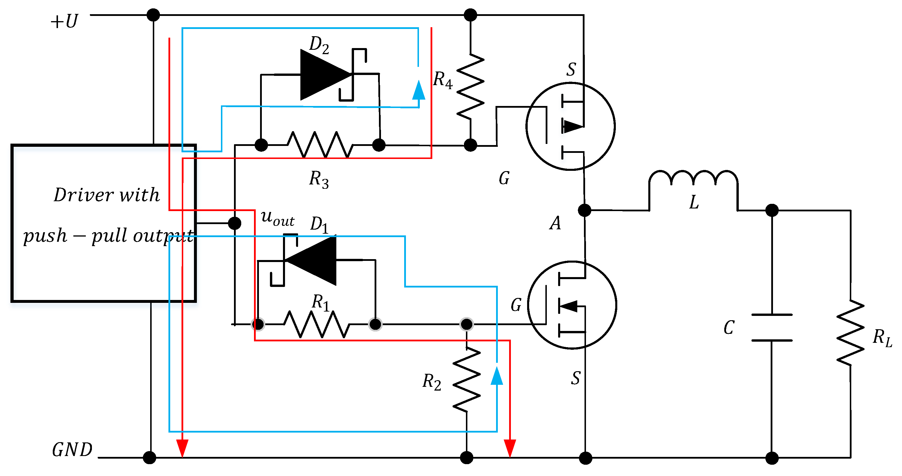
Figure 2.
CH1 – supply voltage 3.3V, CH2 – voltage at point A.
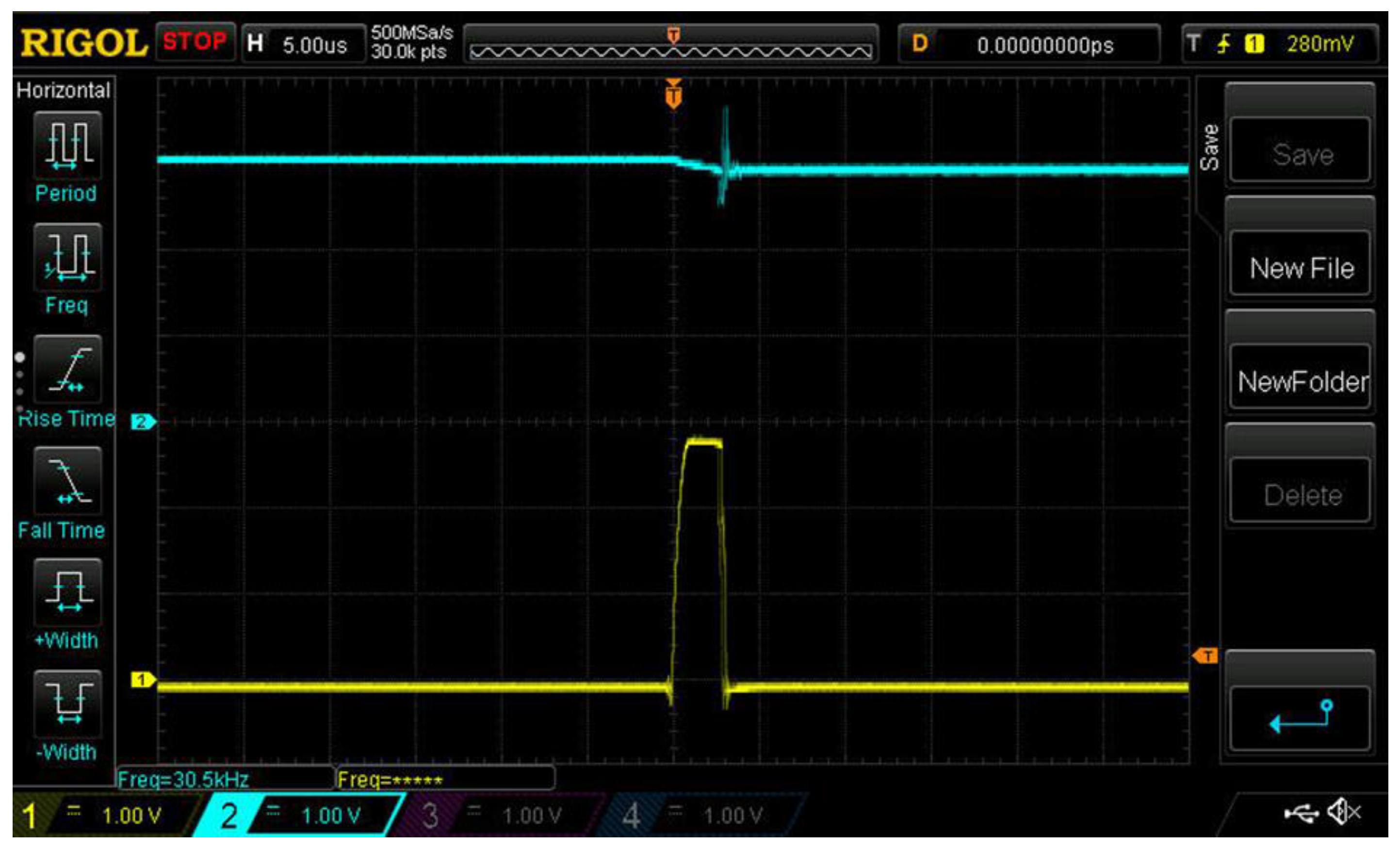
Figure 3.
CH1 – the impulse of the lower transistor, CH2 – the voltage at point A.
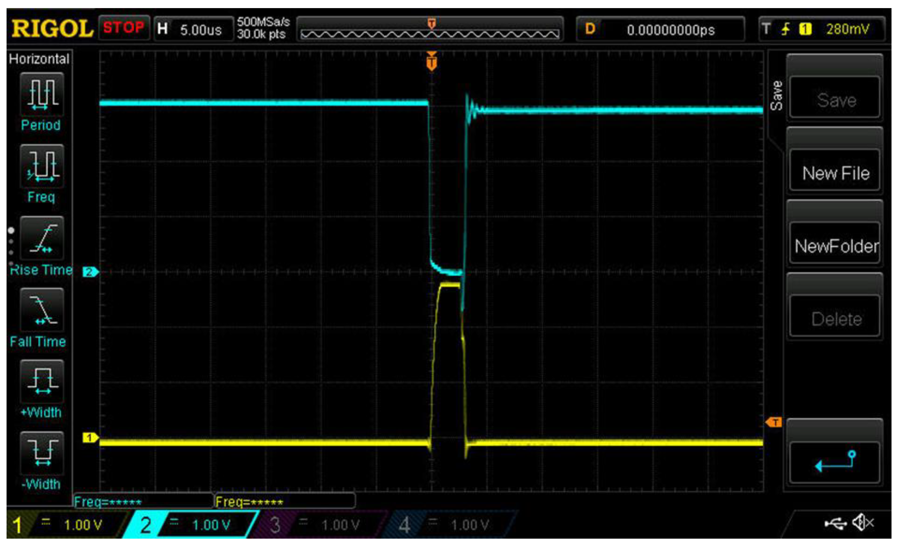
Figure 4.
Scheme for studying the influence of the Schottky diode capacitance when applying a signal to turn on the transistor.
Figure 4.
Scheme for studying the influence of the Schottky diode capacitance when applying a signal to turn on the transistor.
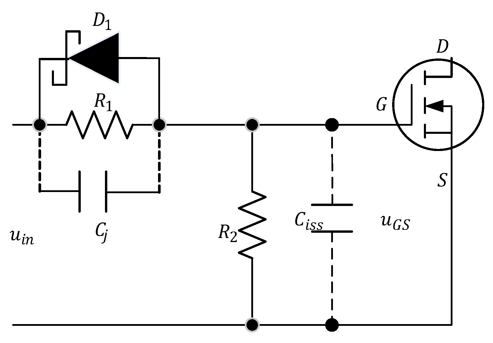
Figure 5.
Mathematical description scheme -.
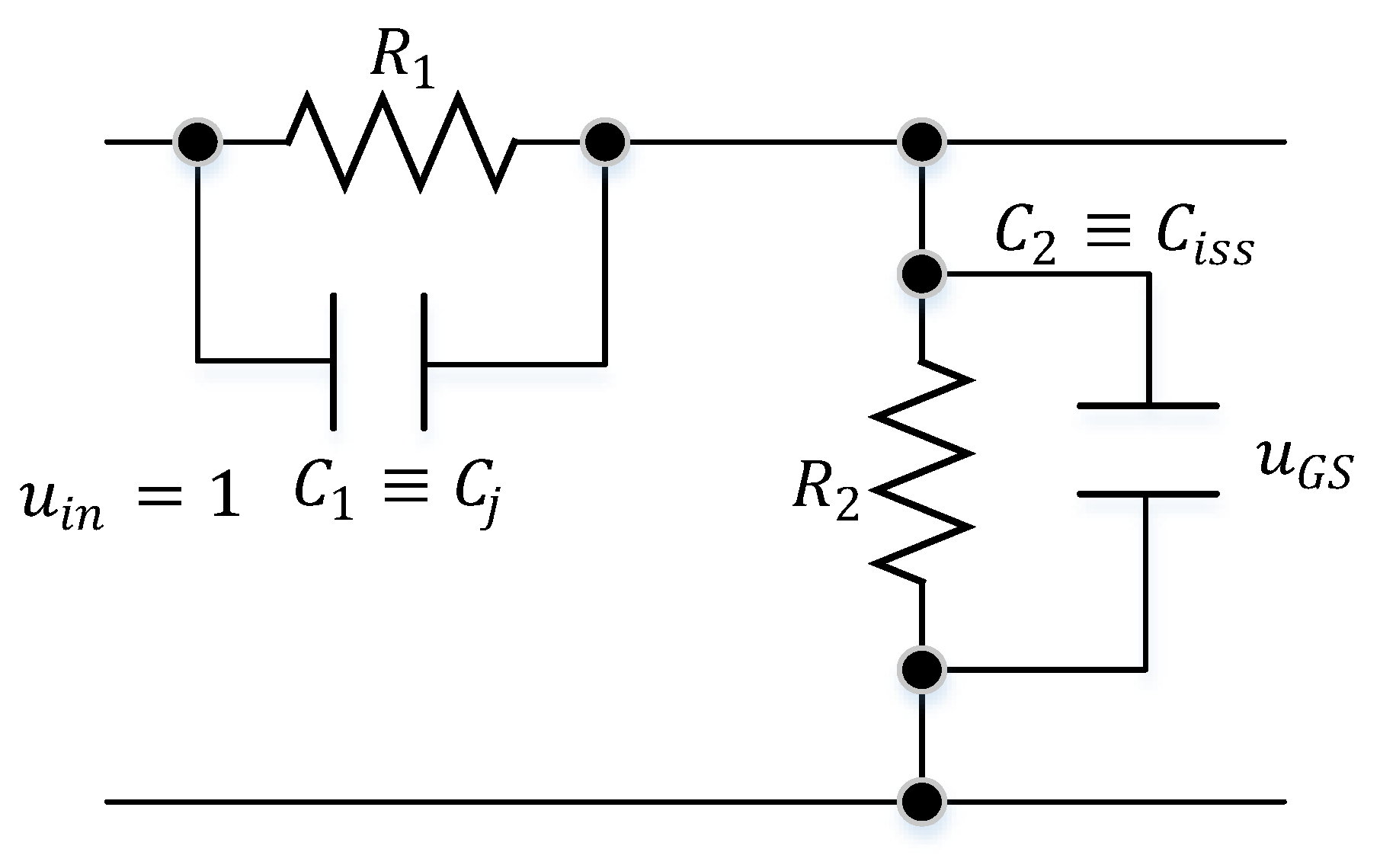
Figure 6.
Variation of the output voltage over time - the red line.
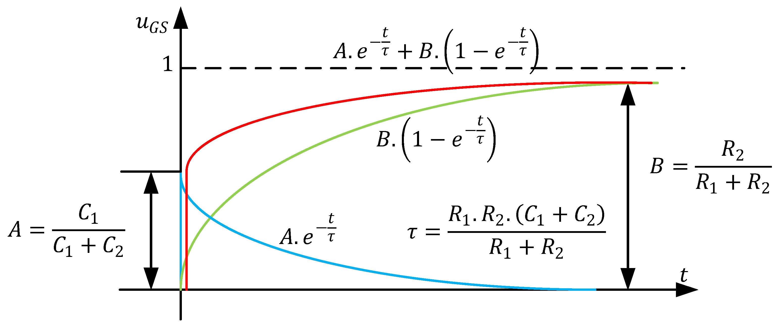
Figure 7.
Simulation scheme and results for variant 1.
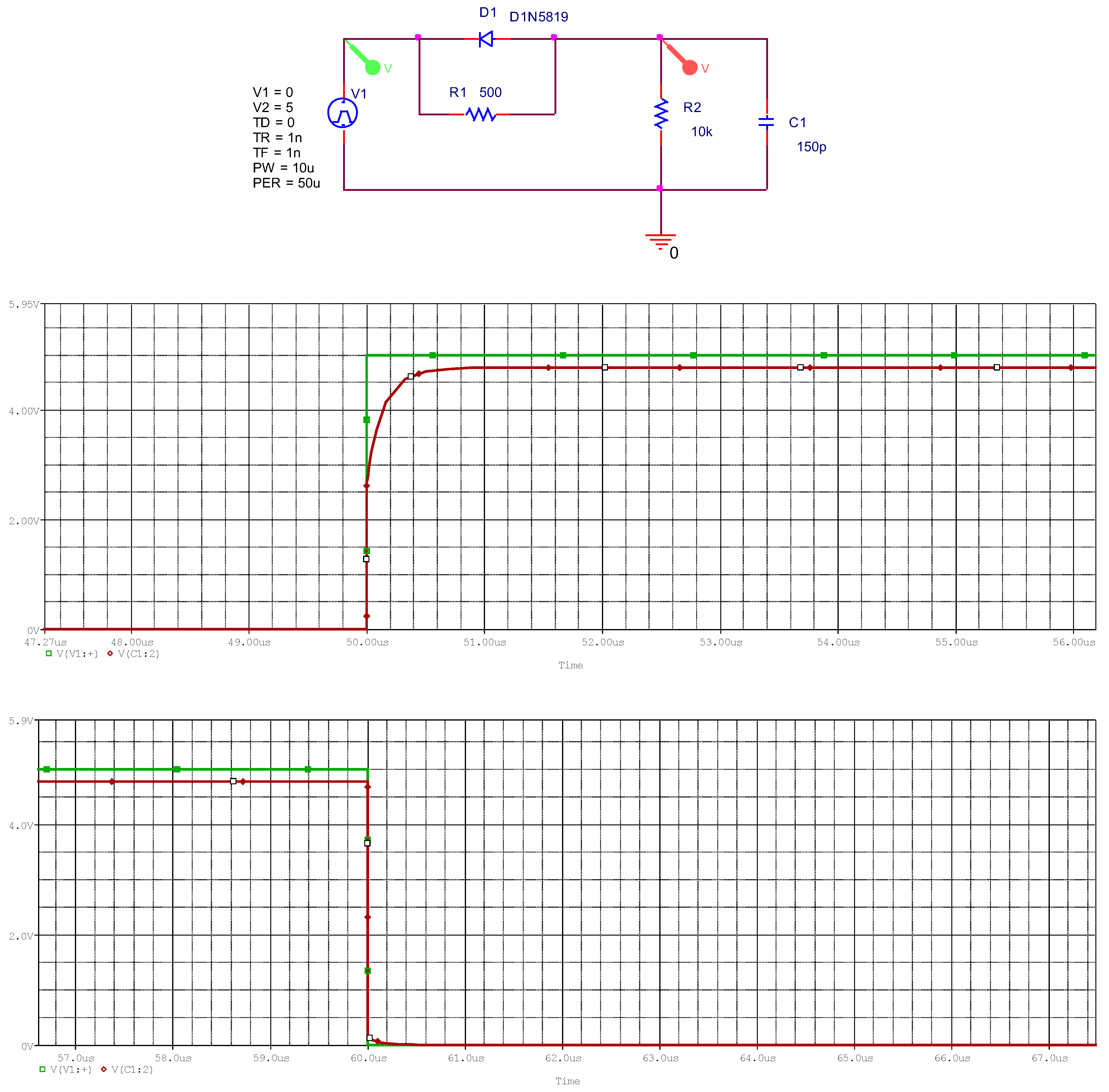
Figure 8.
Simulation scheme and results for variant 2.
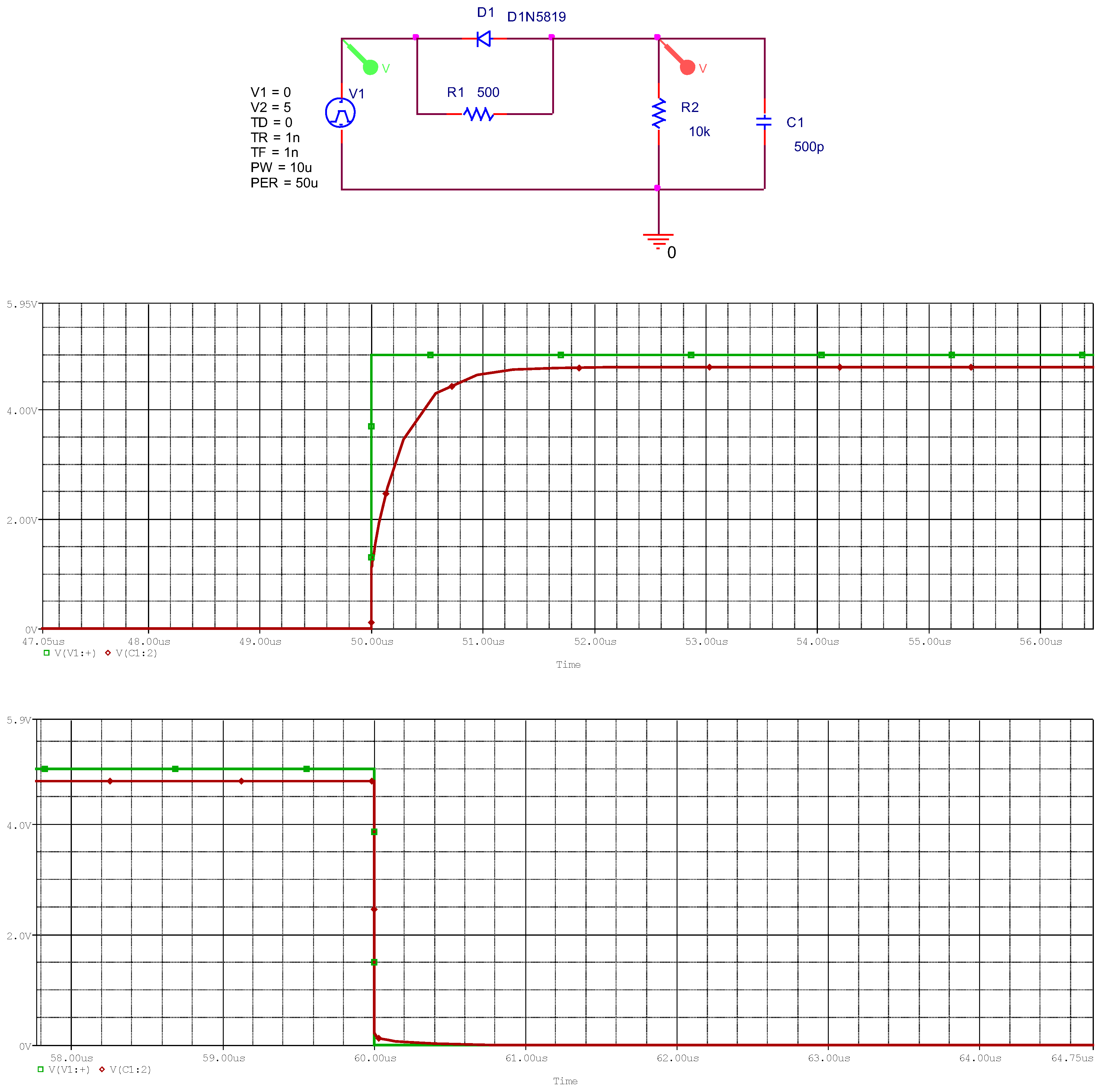
Figure 9.
Simulation scheme and results for variant 3.
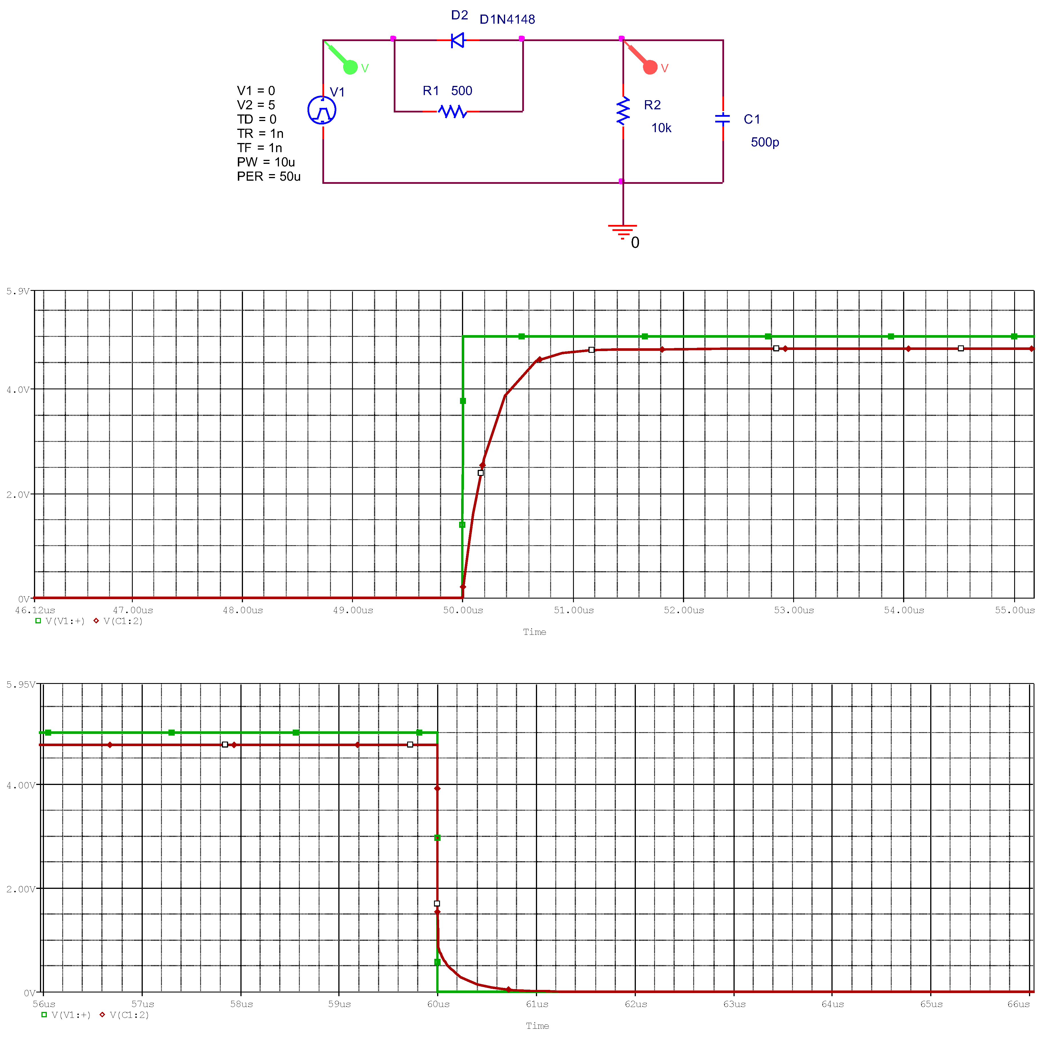
Figure 10.
Connecting a zener diode in parallel with the gate-source junction of the transistor.
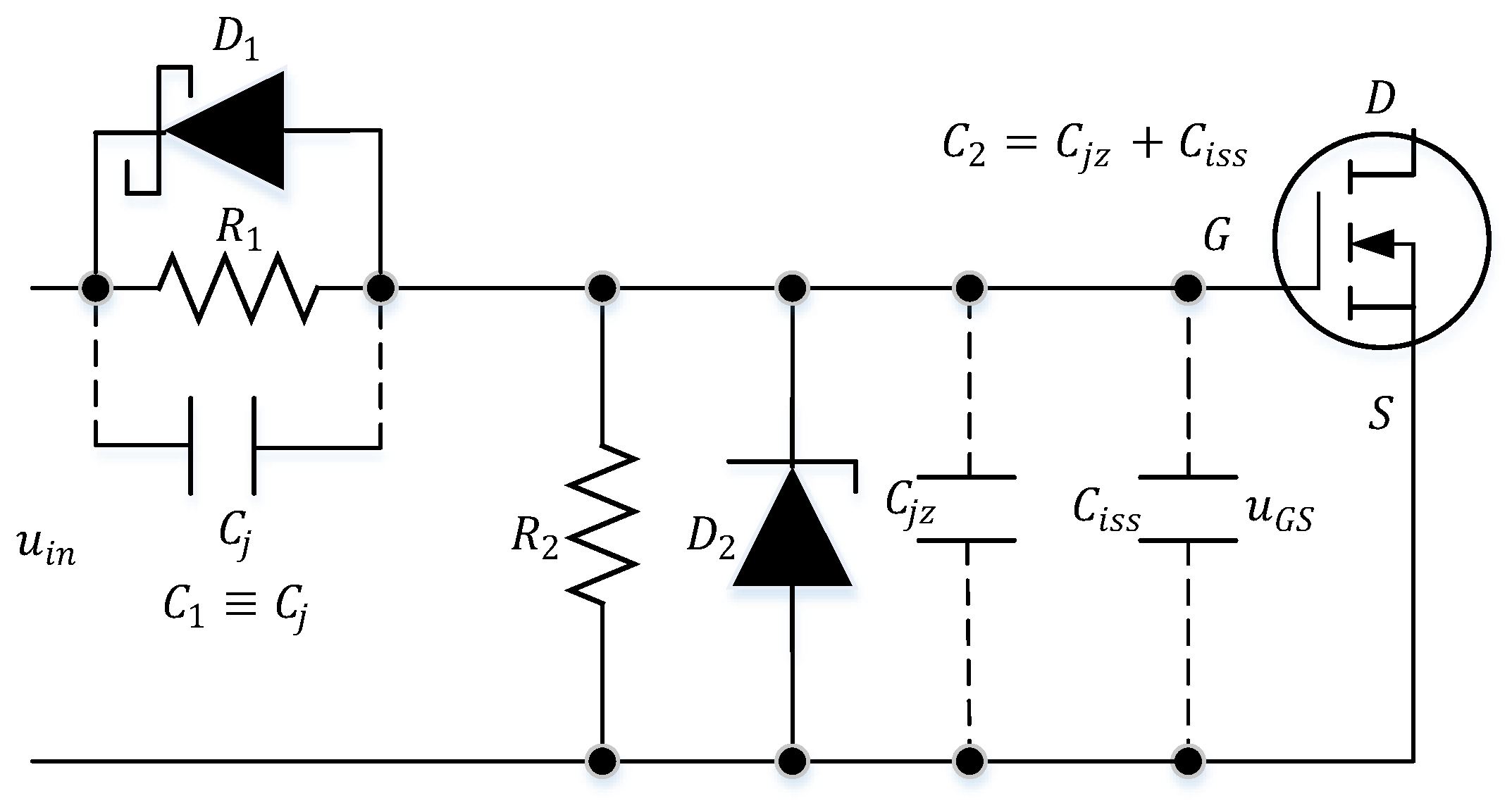
Figure 11.
Simulation scheme and results for variant 4.

Figure 12.
A picture of the power schematic part.
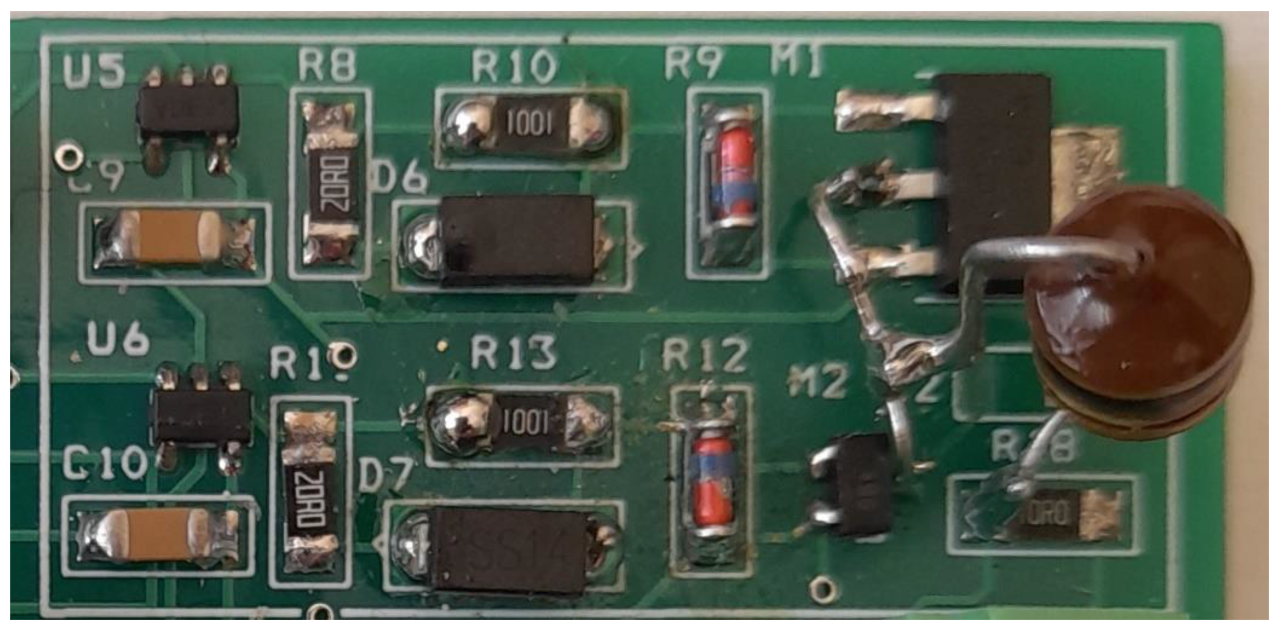
Figure 13.
CH1 - the voltage in point A; below it CH2 - pulses to control the lower transistor.
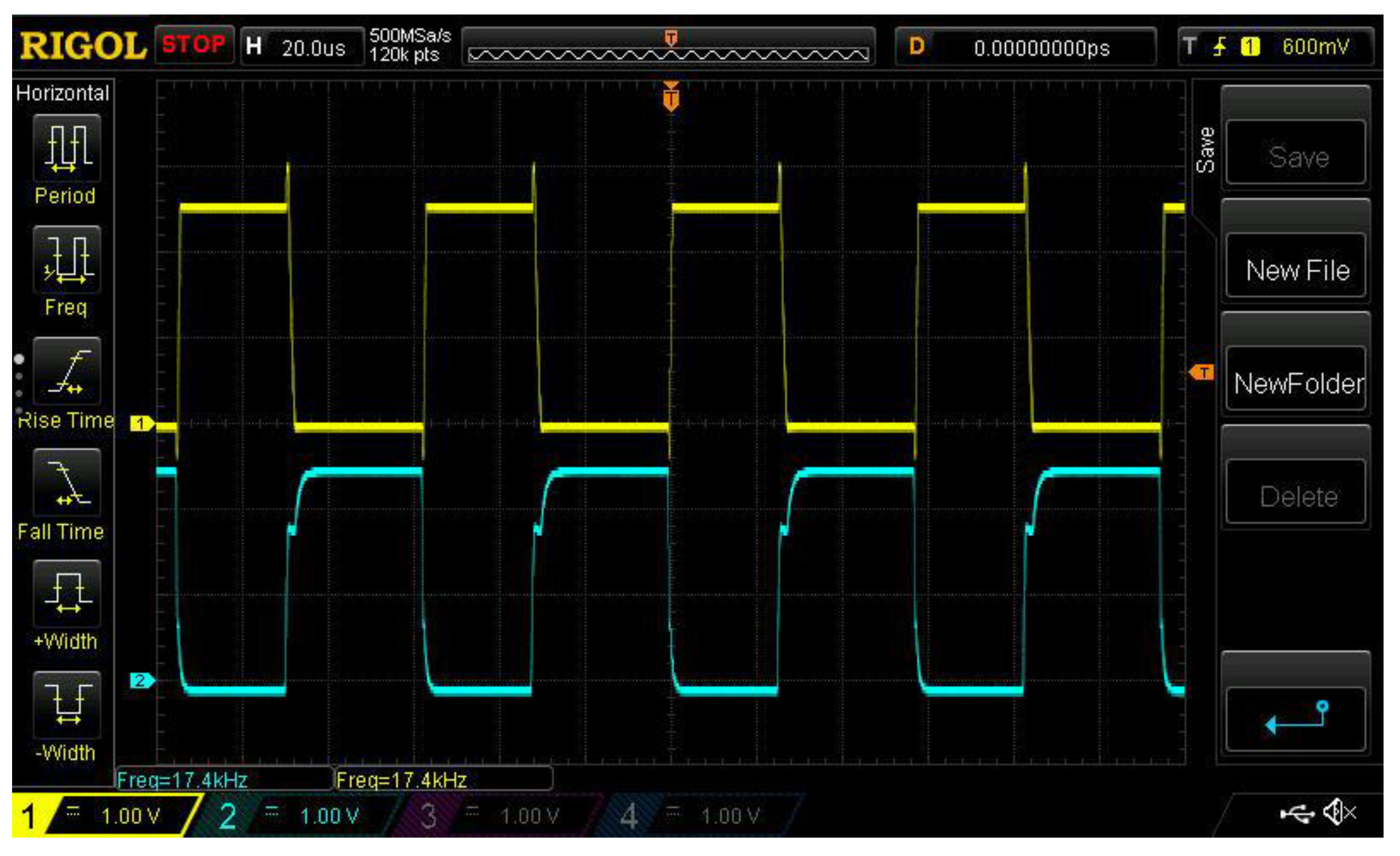
Figure 14.
CH1 - the control pulses of the lower transistor, below them CN2 - the supply voltage.
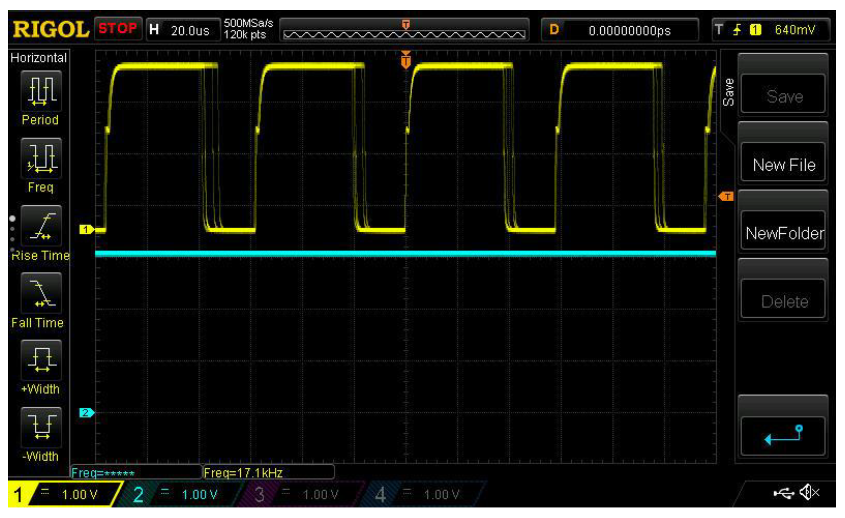

Table 1.
Variants for providing “dead time” for a signal to turn on the lower transistor.
| Schottky diode (Diode) Capacitance, pF | Transistor, Zener diode Capacitance, pF |
Value of A, Starting voltage G-S at 3V from the driver, V |
, min. value, V | |
|---|---|---|---|---|
| Variant 1 | SS34, | BSS214N, |
0.837, 2,51V |
0.7 |
| Variant 2 | SS34, | UT6402G, |
0.654, 1.962V |
1.0 |
| Variant 3 | SS14, | UT6402G, |
0.345, 1.035V |
1.0 |
| Variant 4 | SS14, | UT6402G, , BZM55C5V1, |
0.277, 0.831V |
1.0 |
| Variant 5 | 1N4148W-G, |
UT6402G, |
0.0075, 0.0225V |
1.0 |
| Variant 6 | 1N4148W-G, |
UT6402G, , BZM55C5V1, |
0.00544, 0.0163V |
1.0 |
Table 2.
Ensuring the off state of the lower transistor through the feedback capacitance when the upper transistor is turned on.
Table 2.
Ensuring the off state of the lower transistor through the feedback capacitance when the upper transistor is turned on.
| Schottky diode (Diode), forward voltage, V Driver output low voltage, V |
UT6402G, |
Value of sstarting voltage G-S at 3V from D-S,V | , min. value, V | |
|---|---|---|---|---|
| Variant 4 |
SS14, , LPV7215, Total 0.6V<1V |
UT6402G, , BZM55C5V1, |
0.4V | 1.0 |
| Variant 5 |
1N4148W-G, LPV7215, Total 1.05V>1V |
UT6402G, |
0.523V | 1.0 |
| Variant 6 | 1N4148W-G, LPV7215, Total 1.05V>1V |
UT6402G, , BZM55C5V1, |
0.4V | 1.0 |
Disclaimer/Publisher’s Note: The statements, opinions and data contained in all publications are solely those of the individual author(s) and contributor(s) and not of MDPI and/or the editor(s). MDPI and/or the editor(s) disclaim responsibility for any injury to people or property resulting from any ideas, methods, instructions or products referred to in the content. |
© 2025 by the authors. Licensee MDPI, Basel, Switzerland. This article is an open access article distributed under the terms and conditions of the Creative Commons Attribution (CC BY) license (http://creativecommons.org/licenses/by/4.0/).
Copyright: This open access article is published under a Creative Commons CC BY 4.0 license, which permit the free download, distribution, and reuse, provided that the author and preprint are cited in any reuse.


