1. Introduction
Compared to traditional fuel vehicles, new energy vehicles produce significantly lower carbon emissions, which plays a critical role in reducing air pollution and addressing climate change. As China has already surpassed the United States to become the largest emitter of carbon dioxide, transitioning to electric vehicles is one of the key measures to achieve carbon peaking and carbon neutrality goals. The Insulated Gate Bipolar Transistor (IGBT) plays an indispensable role in today’s new energy vehicle technology. As a core component of the electronic power system in electric vehicles, IGBTs are responsible for efficiently converting and controlling electric energy. Most of the energy losses in inverters are caused by IGBT devices, and these losses directly impact the energy efficiency of electric vehicles while significantly affecting their driving range and reliability [
1]. Excessive losses not only reduce the efficiency of the inverter but also increase the junction temperature of the IGBT module, thereby shortening its lifespan. Moreover, IGBTs are the most failure-prone components within inverters, and the reliability of their operation is closely linked to the overall reliability of the inverter system.
Since the electrical and thermal characteristics of IGBTs are strongly coupled, their simulation studies must comprehensively account for these coupling effects to reliably simulate the real-world operating conditions of IGBT modules and accurately calculate their power losses. Literature [
2] used electro-thermal coupled simulation to incorporate the dynamic relationship between electrical parameters such as current and voltage and temperature variations during switching transients into the IGBT switching model. Meanwhile, literature [
3] analyzed the impact of IGBT device parameters on power losses during their switching operation.
Loss calculation methods can be broadly classified into two categories: physical structure-based methods and mathematical model-based methods. Physical structure-based methods calculate losses by deeply analyzing the internal components of the IGBT, such as resistors, capacitors, and inductors, which provide high accuracy but require significant expertise. In contrast, mathematical model-based methods estimate losses using parameters provided in datasheets, relying on mathematical computations. These methods are more straightforward and user-friendly but may not achieve the same level of precision as the physical structure-based approaches [4-6].
This paper leverages the unique loss analysis functionality of the PLECS simulation software to analyze the losses of IGBT modules. By comparing the errors between simulation experiments and theoretical calculations, this study aims to provide a deeper understanding and effective solutions for improving the energy efficiency and optimizing the systems of electric vehicles.
2. Thermal Simulation of IGBT
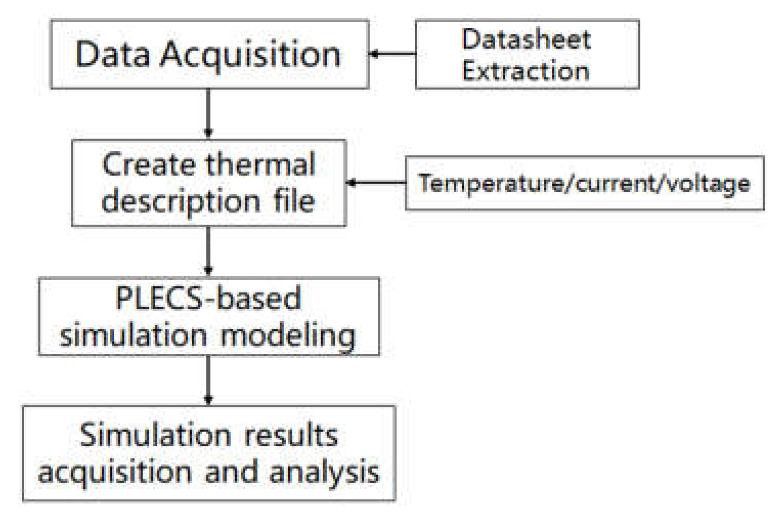
The thermal simulation of IGBT modules aims to accurately estimate their power losses and thermal behavior under various operating conditions, thereby optimizing the thermal management design of the modules. Typically, the thermal simulation process for IGBT modules relies on output characteristics, transfer characteristics, and other data provided in the datasheets from the manufacturers. These datasheets are used to establish thermal description files for IGBTs and anti-parallel diodes within the PLECS simulation software. These files include loss curves for IGBTs and diodes under different temperatures, voltages, and operating currents. In more advanced versions of PLECS, users can directly extract curve data from switch characteristics graphs in datasheets, making it more convenient and efficient to create thermal description files[
7].
Figure 1.
Thermal Simulation Flowchart.
Figure 1.
Thermal Simulation Flowchart.
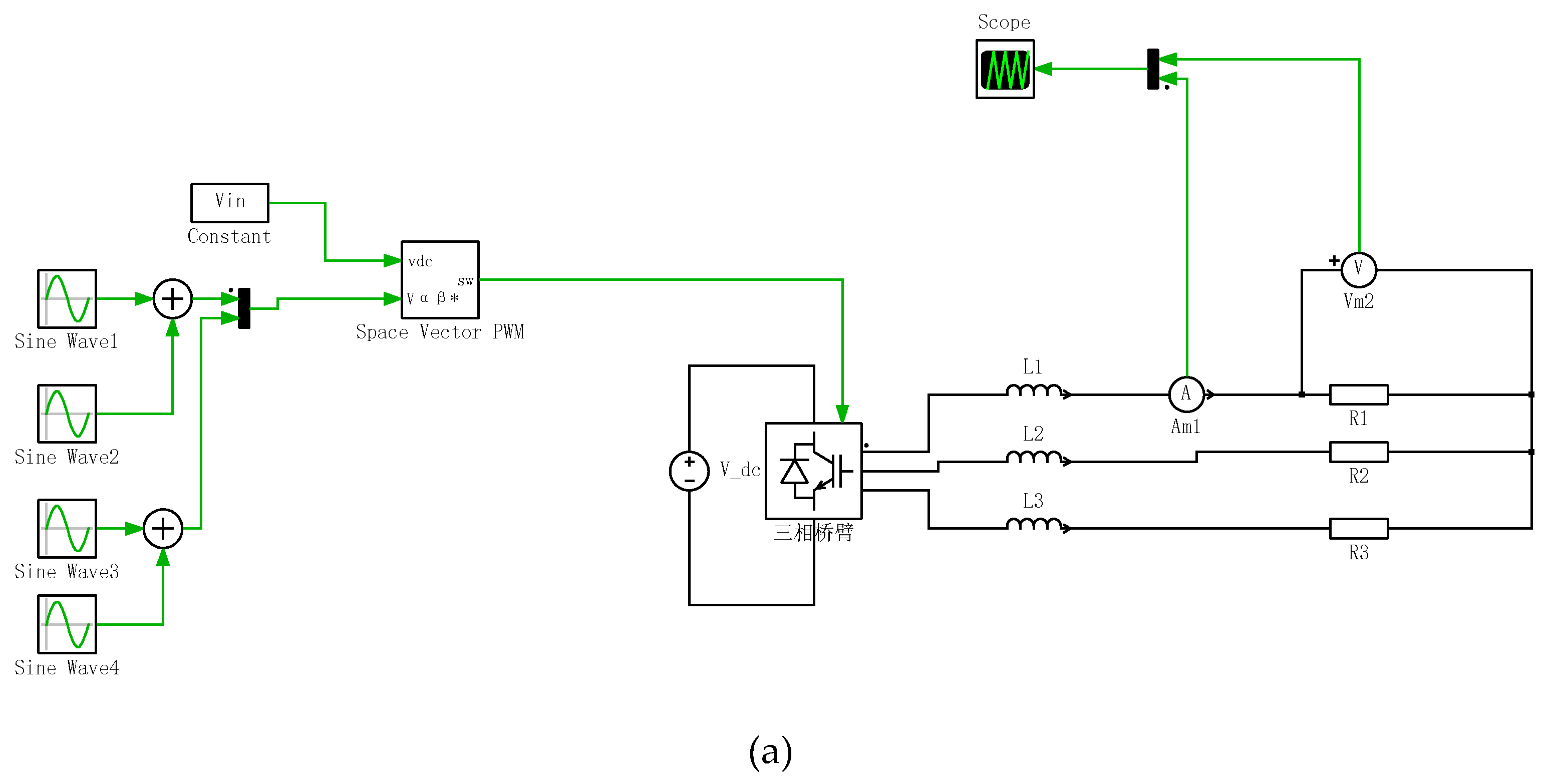
For this study, we selected the SGM820PB8B3TFM IGBT module (820A/750V) from Silan Microelectronics, which is developed using a proprietary high-density trench process, to investigate the loss characteristics of high-power IGBT modules used in electric vehicles. Based on the inverter environment, an open-loop control system simulation model was developed in PLECS, as shown in
Figure 2(a). To study the temperature rise of the Heat Sink module caused by power losses, the heat dissipation module was modeled as a thermal chain composed of thermal resistance and thermal capacitance, connected to an external constant-temperature source. Initially, the temperature of the heat sink, environment, and thermal components was set to 25°C. The number of layers in the thermal chain, ranging from the IGBT chip to the environment, determines the thermal resistance and capacitance of each layer, with values derived from the datasheet. When thermal equilibrium is reached, the heat sink temperature stabilizes. Given that the duty cycle of the control signal varies between 0 and 1, calculating the conduction losses during post-processing can be cumbersome. Therefore, the average losses were calculated using a periodic averaging module and a pulse averaging module, both configured with switching frequency parameters.
Using Space Vector Pulse Width Modulation (SVPWM), this modulation strategy can control the turn-on and turn-off states of the IGBTs in a three-phase bridge arm, converting DC power into AC power for three-phase resistive-inductive loads. The module generates a reference voltage vector at the AC terminals of the three-phase voltage source inverter, which is defined in the coordinate system as a reference voltage. This reference voltage is defined in the coordinate system as: The output, marked as "sw," consists of three switching control signals [Sa, Sb, Sc], which control the upper and lower switches of the inverter branches A, B, and C, respectively. Each switching signal controls the upper and lower switches in its corresponding branch. Unlike calculating the conduction times of switch vectors and zero vectors, this module uses an equivalent index-based modulation method to manipulate the three-phase sinusoidal modulation indices through various zero-sequence injection patterns, thereby achieving different SVPWM modulation strategies.
The module is implemented as a series connection of a modulation module based on three-phase indices and a symmetric PWM module. The symmetric PWM module is configured to use a conventional sampling scheme (minimum single update), where the incoming modulation indices are sampled only at the minimum points of the symmetric triangular carrier waveform. The module allows setting different modulation strategies, including Symmetrical, DPWM0, DPWM1, DPWM2, DPWM3, DPWMMIN, and DPWMMAX. The symmetrical strategy always uses two zero vectors (V0 and V7), placing one in the center of the period and evenly spacing the other at the start and end of the period. DPWM1, DPWM2, and DPWMMAX produce identical switching patterns within 30-degree intervals, using only one zero vector (V7) in this interval, evenly distributed at the start and end of the period. DPWM0, DPWM3, and DPWMMIN also generate identical switching patterns within the 30-degree intervals, using a single zero vector (V0), which is placed at the center of the period. All these strategies adhere to the same space vector modulation theory, with the primary differences lying in how the two available zero vectors (V0 and V7) are distributed within each switching cycle across different sector intervals.
The output switching values alternate between high and low states. The selection of these values should match the gate control logic of the inverter, where a high value turns on the upper switch in the bridge arm, and a low value turns on the lower switch. The default values are [-1, 1]. Calculations show that the amplitudes of the four sinusoidal waveforms input to the SVPWM module are: Im*R、-2*fg*Im*Lf*pi、2*fg*Im*Lf*pi、Im*R; all frequencies are fg, and the phases are 90°, 0°, 90°, and 90°, respectively.
As shown in
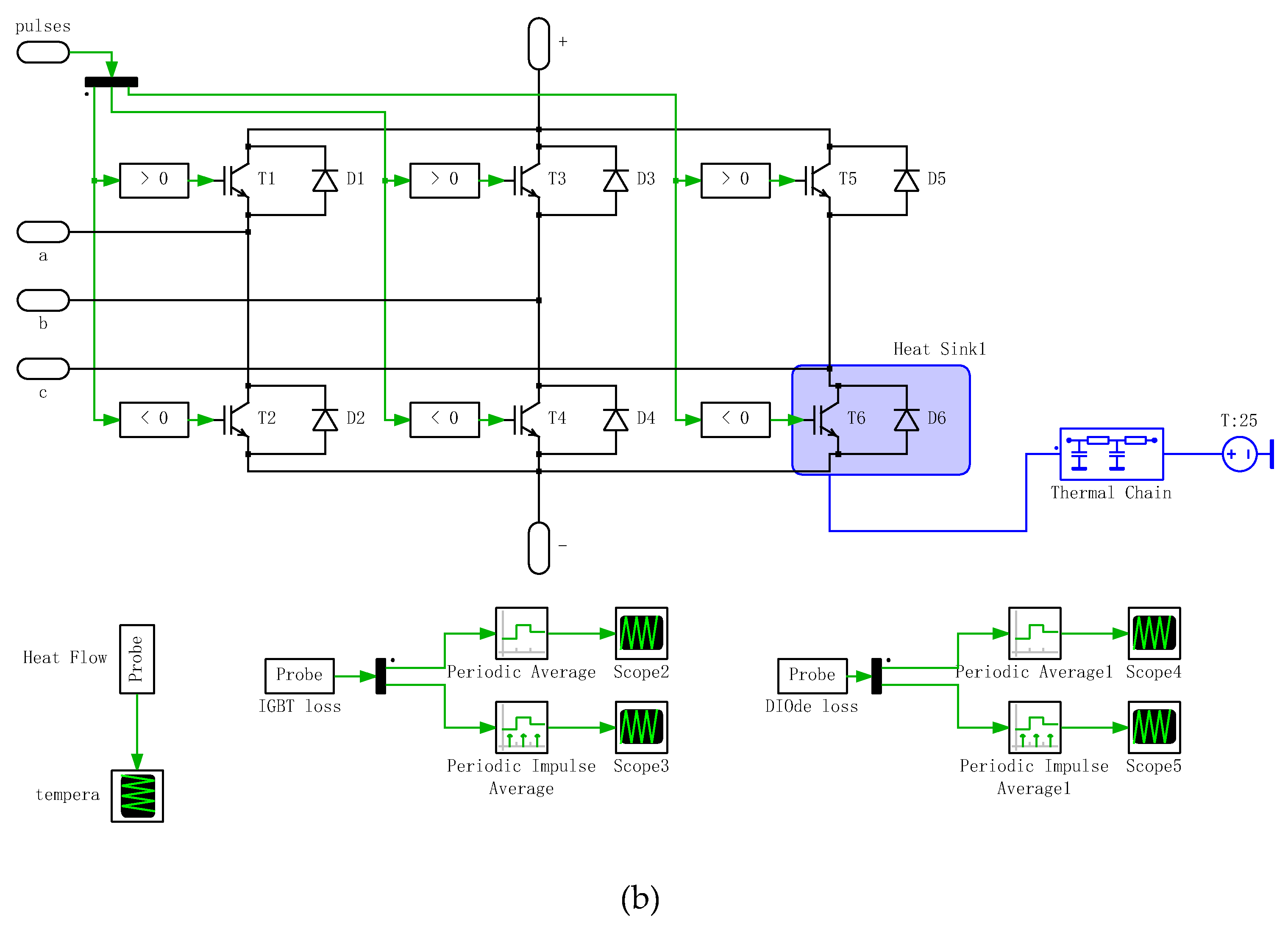
Figure 2(b), the internal structure of the three-phase bridge arm module incorporates six IGBTs with anti-parallel diodes. The parameters can be set according to the transfer characteristic curves, output characteristic curves, and other data provided in the datasheets of the IGBT modules. Through simulation, the conduction losses and switching losses of the IGBT module can be obtained.
3. Results
When building a simulation model in PLECS based on the manufacturer-provided datasheet, the typical characteristic curves of the IGBT module can be used to construct a loss model.
The simulation parameters are set as follows: switching frequency of 10 kHz, DC voltage of 500 V, AC current amplitude of 30 A, load inductance of 1 mH, and load resistance of 1 Ω.
For device losses, the specific loss values can then be obtained by consulting the three-dimensional loss table built into the software based on these operating condition data.
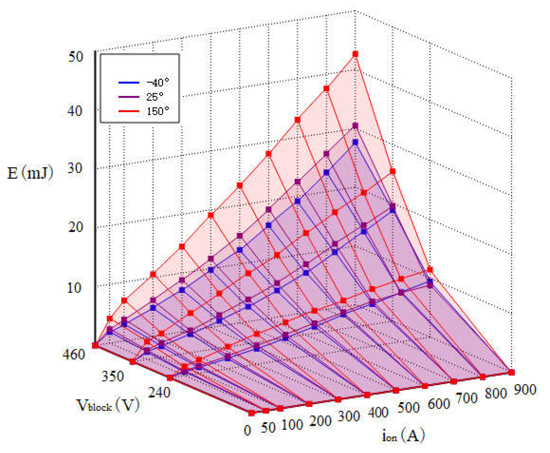
The energy losses E
on and E
off of IGBT during a switching process are not constant; they depend on the collector current and the junction temperature. From the switching characteristics, it is evident that E
on and E
off increase with higher current. When the current is constant, higher junction temperatures also result in larger E
on and E
off, indicating a positive temperature coefficient. Therefore, establishing an accurate switching model in PLECS is essential, as illustrated in
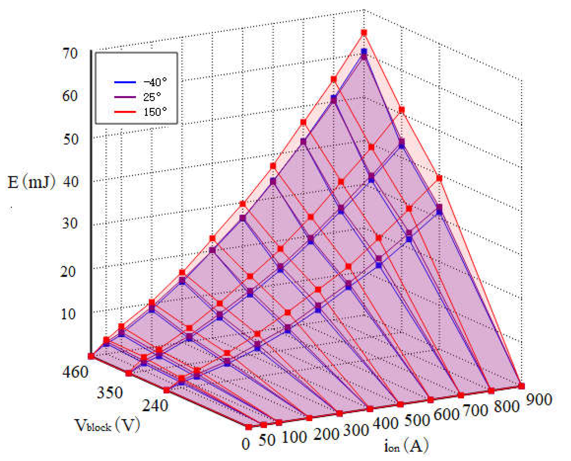
Figure 3 and
Figure 4.
Figure 3 and
Figure 4 show the turn-on losses and turn-off losses of the IGBT module in different states during simulation. Through these results, we can closely observe the loss behavior of the IGBT module under specific operating conditions, particularly the impact of temperature and current variations on switching losses.
Figure 3 shows the loss curve of the IGBT module during the turn-on process. The shape of the curve indicates that the turn-on losses increase gradually as the collector current increases. This relationship can be explained by the positive temperature coefficient in the thermal model, where the turn-on losses of the IGBT significantly increase under high-temperature conditions.
Figure 4 illustrates the loss characteristics of the IGBT module during the turn-off process. Similar to turn-on losses, turn-off losses also increase with rising current and temperature. These simulation results demonstrate the significant impact of temperature and current on the switching performance of the IGBT module, providing data support for subsequent optimization efforts.
Detailed analysis of the simulation results reveals distinct differences in the loss characteristics of the IGBT module under different switching states. Specifically, as the temperature rises, both the turn-on and turn-off losses of the IGBT increase, which is related to the nonlinear coupling effect between thermal resistance and current. Moreover, the data from
Figure 3 and
Figure 4 indicate that higher junction temperatures will significantly increase power losses, posing greater challenges for thermal management design in electric vehicle systems. Therefore, with the precise calculations of the PLECS simulation model, we can provide effective guidance and optimization strategies for managing the losses of IGBT modules under various operating conditions.
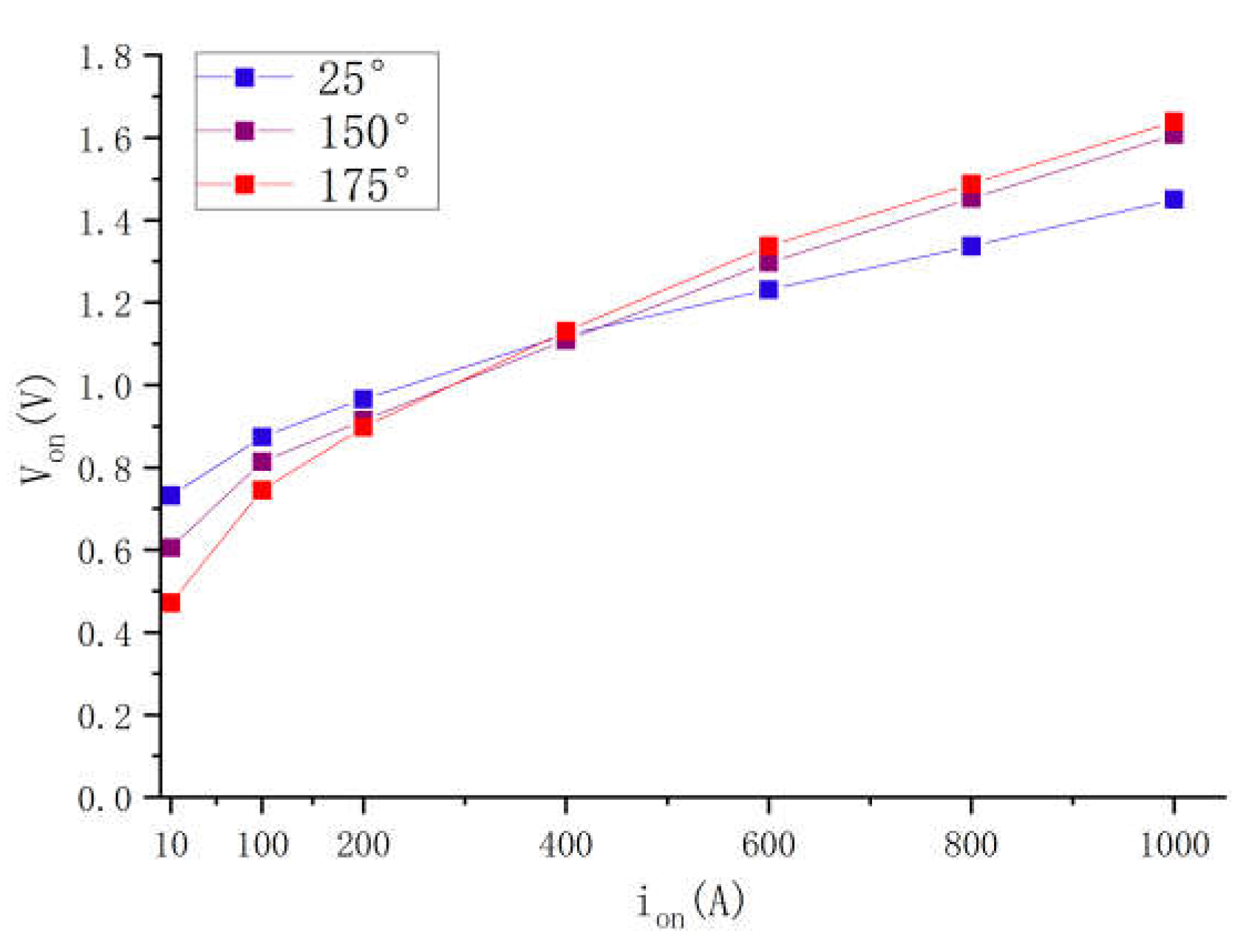
To gain a deeper understanding of the causes of changes in IGBT module losses, we also need to investigate its internal electrical parameters, particularly the interaction between the collector-emitter voltage (VCE), temperature, current, and other conditions on the overall loss characteristics. The collector-emitter voltage (VCE) is a key factor affecting IGBT losses, and we will further analyze its characteristics and variation patterns below.
The collector-emitter voltage (V
CE) continuously varies and is associated with its current and junction temperature. Its output characteristic curve in the thermal loss model in PLECS is shown in
Figure 5. From its characteristics, it can be seen that when the current is higher, the junction temperature under the same current is also higher, and the collector-emitter voltage is larger, indicating a positive temperature coefficient. Conversely, a lower collector-emitter voltage corresponds to a negative temperature coefficient. At a given junction temperature, the larger the current, the greater the collector-emitter voltage, indicating a positive correlation between V
CE and current. Therefore, it is essential to establish an accurate thermal model in PLECS to calculate the collector-emitter voltage.
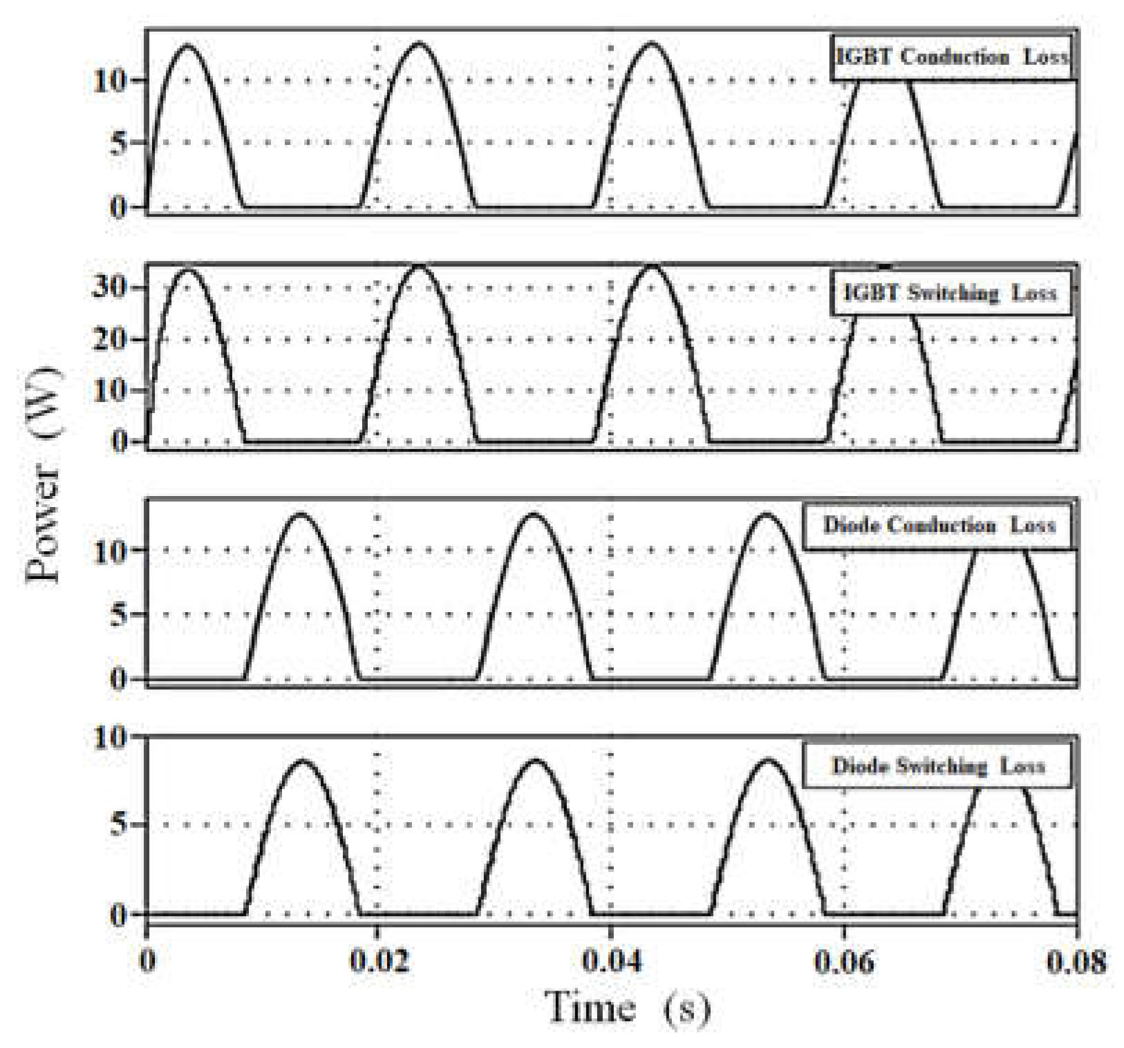
The conduction loss of the IGBT module can be obtained using the Periodic Average module in the PLECS library browser, while the switching loss can be calculated using the Periodic Impulse Average module, as shown in
Figure 6.
A validation analysis was conducted by comparing the theoretical results with the PLECS simulation results.
Based on the modulation principle of Space Vector Pulse Width Modulation (SVPWM)[8-11], taking the upper IGBT module (T and D1) of phase a bridge arm in the inverter as an example, the conduction time
ton of this semiconductor device in one switching cycle is:
The conduction duty cycle D of the upper IGBT module in the phase-a bridge arm can be calculated as:
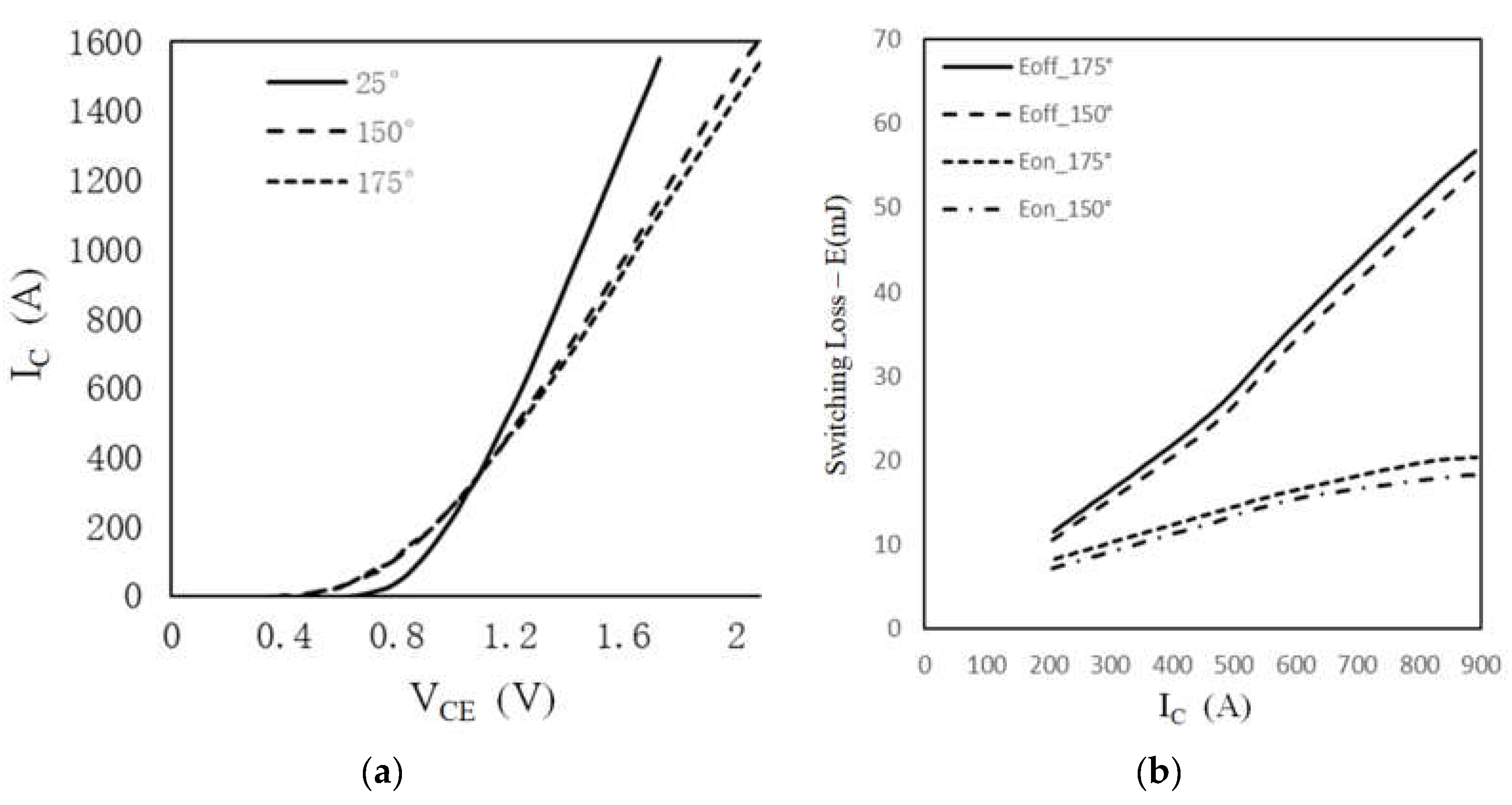
In the formula: represents the switching period, is the time from the peak of the modulation wave to the edge of the switching wave. The parameter curves of the IGBT module can be extracted from the IGBT datasheet, as shown in the figure:
The relationship curve between the conduction voltage drop V
CE , the conduction current I
C , and the junction temperature T
j is shown in
Figure 7(a). The relationship between V
CE, I
C , and T
j can be obtained through interpolation and curve fitting, expressed as:
The relationship between the energy consumed during one turn-on (E
on) and turn-off (E
off) of the IGBT module and I
C can be fitted based on
Figure 7(b), expressed as:
The relationship between E
on, E
off, and the junction temperature T
j can be expressed as:
Here, Eon-125 represents the energy loss for one turn-on at 125℃, and Eoff-125 represents the energy loss for one turn-off at 125℃. Similarly, the same principle applies to the diode, and based on this, the loss calculation model for the IGBT module can be established.
The conduction loss of the IGBT during one turn-on and turn-off cycle can be expressed as:
Here, represents the instantaneous current flowing through the IGBT.
The switching loss generated during each turn-on and turn-off of the IGBT is:
The conduction loss of the FWD (freewheeling diode) during one turn-on and turn-off cycle is:
Here, Dd represents the conduction duty cycle of the FWD within the period.
The reverse recovery loss generated by the FWD during each turn-on and turn-off is:
The simulation model results and theoretical calculation results are shown in the table below.
To verify the validity of the simulation model proposed in this paper, a comparative analysis was conducted between the simulation results and the typical algorithm. Typical algorithms usually rely on static parameters provided in the IGBT datasheet and calculate conduction and switching losses using mathematical models. However, because this method fails to fully account for the dynamic changes of IGBT devices under complex operating conditions such as temperature and frequency, its accuracy is limited under extreme conditions like high temperature or high frequency. In contrast, the simulation model proposed in this paper offers significant advantages, meeting more stringent operational requirements in terms of both accuracy and applicability.
4. Discussion
In the process of comparing the simulation results with the typical algorithm, we found that the loss characteristics of the IGBT are influenced by multiple factors simultaneously. These key factors include junction temperature, collector current, voltage, and switching frequency, all of which exhibit complex coupling relationships. Specifically, an increase in junction temperature leads to higher turn-on and turn-off losses, which is due to the decreased conductivity of semiconductor materials at elevated temperatures. Similarly, an increase in collector current also exacerbates conduction and switching losses because higher current demands more energy to drive the switching operation. Furthermore, an increase in the collector-emitter voltage (VCE) directly results in greater switching losses. These factors are often not independent but interact with and amplify each other's effects. For example, higher switching frequency not only increases switching losses but also causes further elevation of the junction temperature. Therefore, when optimizing the loss management of IGBT modules, it is essential to comprehensively consider the interactions of these factors to ensure system stability and efficiency.
5. Conclusions
For the three-phase inverter system of electric vehicles under the SVPWM modulation method, this paper studies the IGBT module losses by using the IGBT datasheet to establish a three-dimensional lookup table model in the PLECS software. The simulation speed has been improved, and the accuracy of loss calculation in the estimation of IGBT module junction temperature in the simulation model has been enhanced. The simulation results indicate that the proposed simulation model achieves high accuracy, with a calculation error of less than 4%. Therefore, this method is suitable for the precise calculation of losses in IGBT modules for electric vehicles.
Author Contributions
Conceptualization, Wang Feng and Dou Wang; methodology, Wang Feng, Dou Wang, Song Yifan, Zheng Chao Lei and Li Zhuang Zhuang; software, Wang Feng; writing—original draft preparation, Dou Wang and Song Yifan.; funding acquisition, Zheng Chao Lei and Liu Jun. All authors have read and agreed to the published version of the manuscript.
Funding
This research received no external funding.
Data Availability Statement
Data are available from the authors upon reasonable request.
Acknowledgments
This research was supported by Chongqing technology innovation and application demonstration project (CSTB2022TIAD-DEX0015) and Key project of Chongqing Natural Science Foundation Innovation and Development Joint Fund(CSTB2024NSCQ-LZX0158)
Conflicts of Interest
The authors declare no conflicts of interest.
References
- Zhang Sihui, Zhao Rui, Yan Shuai, et al. Method for Monitoring the Junction Temperature of Power Devices in Three-phase Inverters Based on the Thermal Resistance Model [J]. Journal of Power Supply, 2021, 19, 27–34. [Google Scholar]
- Tang Yong, Wang Bo, Chen Ming. Temperature Characteristics and Electro-Thermal Simulation Model of IGBT Switching Transients [J]. Transactions of China Electrotechnical Society, 2012, 27, 146–153. [Google Scholar]
- Mirizadeh A, Baroogh F A, Gheydi M, et al. Evaluation of conduction and switching losses in cascaded multilevel inverters[C]//2017 10th International Symposium on Advanced Topics in Electrical Engineering (ATEE). IEEE, 2017: 124-127.
- Yan Qingzeng, Sun Pengxiao, Zhao Rende. Design of Simulation Experiment for Three-phase Two-level Converter Based on PLECS [J]. Experimental Technology and Management, 2019, 36, 119–122+127. [Google Scholar]
- Wang Yangan, Dai Xiaoping, Wu Yibo, et al. Mechanism, Calculation, and Simulation of Power Loss in IGBT Modules [J]. High Power Converter Technology, 2015, 62-66.
- Huang H, Bryant A T, Mawby P A. Electro-thermal Modelling of Three-phase Inverters [C]//Proceedings of the 14th European Conference on Power Electronics and Applications (EPE). IEEE, 2011: 1-7.
- Yao Fang, Wang Shaojie, Li Zhigang. Electro-thermal Coupled Simulation Model of IGBT Power Module in Inverter [J]. Semiconductor Technology, 2016, 41, 440–445+472. [Google Scholar]
- Wang Zheyu, Li Min, Liu Zhiqiang. Simulation Study on the Electro-thermal Performance of Power Units [J]. Automotive Engineer, 2023, 11-15+21.
- Du Yi, Liao Meiying. Loss Calculation of IGBT Module in Inverter and Its Cooling System Design [J]. Electric Drive Automation, 2011, 33, 42–46. [Google Scholar]
- Reichl J R, Lai J S, Hefner A R, et al. Inverter dynamic electro-thermal modeling and simulation with experimental verification[C]//2005 IEEE 36th Power Electronics Specialists Conference. IEEE, 2005: 2208-2215.
- Bai Baodong, Chen Dezhi, Wang Xinbo. Calculation of IGBT Loss in Inverters and Design of Cooling Devices [J]. Transactions of China Electrotechnical Society, 2013, 28, 97–106. [Google Scholar]
|
Disclaimer/Publisher’s Note: The statements, opinions and data contained in all publications are solely those of the individual author(s) and contributor(s) and not of MDPI and/or the editor(s). MDPI and/or the editor(s) disclaim responsibility for any injury to people or property resulting from any ideas, methods, instructions or products referred to in the content. |
© 2025 by the authors. Licensee MDPI, Basel, Switzerland. This article is an open access article distributed under the terms and conditions of the Creative Commons Attribution (CC BY) license (http://creativecommons.org/licenses/by/4.0/).