
Submitted:
30 December 2024
Posted:
02 January 2025
You are already at the latest version
Abstract
This study introduces a comprehensive physical modeling framework for phototransistors based on quasi-two-dimensional (quasi-2D) transition metal dichalcogenides (TMDC), with a particular emphasis on MoS2. By integrating electromagnetic simulations of optical absorption with semiconductor transport calculations, the model captures both dark and photocurrent behaviors across diverse operating conditions. The results accurately reproduce spectral absorption peaks in MoS2 films of varying thicknesses and demonstrate strong agreement with experimental dark current transfer characteristics. A key insight from the study is the critical role of defect states, including traps, impurities, and interfacial imperfections, in governing dark current and photocurrent under channel pinch off conditions. The model successfully replicates the qualitative trends observed in experimental devices, highlighting how small variations in film thickness, doping levels, and contact geometries can significantly influence device performance, in agreement with published experimental data. These findings underscore the importance of precise defect characterization and the optimization of material and structural parameters in phototransistors based on 2D materials. The proposed modeling framework serves as a powerful tool for the design and optimization of next-generation phototransistors, facilitating the integration of 2D materials into practical electronic and optoelectronic applications.
Keywords:
Phototransistor Modeling
; Transition Metal Dichalcogenides
; MoS2 Photodetector
; Quasi-Two-Dimensional Materials
; Optoelectronics
; Photocurrent Analysis
; Optical Absorption
1. Introduction
Two-dimensional (2D) graphene-like materials have become one of the most actively studied classes of substances due to their unique electronic, optical, and mechanical properties [1]. Since the discovery of graphene, a multitude of other 2D materials have been explored, including transition metal dichalcogenides (TMDCs) such as MoS2, WS2, and MoSe2 [2]. These materials exhibit properties such as high carrier mobility, strong light-matter interaction, and mechanical flexibility, making them promising for a broad range of applications in micro- and nanoelectronics, optoelectronics, sensing, and energy storage [3,4,5,6].
Among the most promising TMDC-based devices are transistors, photodetectors, light-emitting diodes, and solar cells. Phototransistors, in particular, have garnered significant attention for their potential to achieve high sensitivity and rapid response times in detecting light across various wavelengths. This potential arises from the direct bandgap of monolayer TMDCs, which simplifies light absorption and facilitates the generation of photonic responses [7,8]. A detailed roadmap for 2D optoelectronics, including opportunities and technological barriers, is presented in [9].
Despite extensive laboratory demonstrations, commercially viable electronic and optoelectronic devices based on 2D materials are still absent from the market. The main obstacle lies in the technological challenges of synthesizing large-area, high-quality films and integrating them into silicon planar technology. Recent advancements in chemical vapor deposition, molecular beam epitaxy, and mechanical exfoliation have made it possible to control certain film parameters, such as thickness, uniformity, and defect density, with sufficient precision for laboratory applications [10]. However, the variability in synthesis methods and resulting material properties continues to hinder the reproducibility and scalability of TMDC-based devices.
Optical devices based on TMDCs are particularly attractive due to the direct bandgap of monolayer films, which enhances photon absorption and response generation. However, as numerous experiments have shown, practical results can vary significantly even for nominally identical materials. These discrepancies arise from differences in synthesis methods, defect densities, layer numbers, structure geometries, and contact configurations. Consequently, the wide range of parameters, including lateral dimensions, thickness, impurity types and concentrations, and interfacial and surface effects, makes direct comparisons between devices challenging without detailed consideration of all influencing factors [11,12].
One of the most powerful tools for addressing these challenges is physical modeling, which allows for the systematic analysis of various device configurations and parameters. Modeling not only predicts device characteristics but also provides deeper insights into the influence of specific parameters, such as film thickness, defect density, and contact geometry. Particularly relevant are models that account for the quasi-2D properties of materials, interfacial effects, and charge transport mechanisms, including thermionic emission, tunneling, and recombination. However, the number of studies performing detailed modeling of this kind remains limited, largely due to the complexity of integrating optical and electrical calculations and the need for precise material parameters such as carrier concentrations, mobilities, and absorption coefficients [13,14].
This study addresses the need for comprehensive modeling of phototransistors based on TMDCs, specifically MoS2 and its quasi-2D thicker films. By combining optical absorption calculations with semiconductor transport modeling, we investigate the role of defects, film thickness, and interfacial phenomena on device performance. The results demonstrate that the proposed model qualitatively reproduces experimental trends and highlights critical factors influencing phototransistor behavior. These findings contribute to the rational design and optimization of 2D-material-based phototransistors, paving the way for their integration into practical applications and emphasizing the importance of advanced physical modeling in modern nanoelectronics.
2. Materials and Methods
To perform reliable physical modeling, it is essential to base the simulation on the geometry of a real device. This approach not only confirms the validity of the modeling results but also ensures their relevance to practical applications by aligning closely with experimentally obtained operational characteristics. It is equally critical to use a two-dimensional material with well-documented optical and electronic properties, as relying on poorly characterized materials could reduce modeling efforts to mere parameter fitting, undermining the physical insight provided.
MoS2 has been traditionally favored for such applications due to its exceptional combination of properties. As a monolayer material, MoS2 exhibits a direct bandgap (~1.8 eV), making it highly efficient for light absorption and electron-hole pair generation in the visible spectrum. Additionally, it demonstrates strong photoconductive responses, high chemical stability, and compatibility with established fabrication techniques. These characteristics position MoS2 as the most studied and widely adopted material for 2D phototransistors [15].
Also important is the method of creating two-dimensional films. Mechanical exfoliation is the preferred approach as it ensures minimal defect density in the material. This simplifies the modeling process by reducing the complexities associated with non-uniform defects, thereby enhancing the accuracy and reliability of simulations when compared to experimental data [16].
For this study, the work [17] was chosen as an ideal reference. This selection is particularly advantageous because the authors provided not only experimental results on the optical properties and operational characteristics of the devices created but also other critical experimentally derived data on the material properties. While the referenced study employed quasi-two-dimensional MoS2 films, this does not pose a significant limitation as long as all optical and electronic parameters for the material are well-documented. Furthermore, the availability of experimental data for films with varying thicknesses and geometries enables a more thorough validation of the proposed model, ensuring its accuracy and applicability across a range of device configurations.
The schematic representation of the selected phototransistor design is shown in Figure 1. It features a quasi-two-dimensional MoS2 layer positioned on a dielectric film—50 nm of Al2O3—which, in turn, is supported by a Si substrate. Al2O₃ was chosen for its higher absorption coefficient compared to SiO2, which not only reduces the device’s energy consumption but also aids in visualizing the quasi-2D material layers.
In this study, transitioning to a 2D model geometry was deemed optimal due to the system's inherent depth symmetry. Unlike in the actual experimental setup, the electrodes in the model are connected laterally to the quasi-2D layer rather than being deposited on top. This simplification serves two purposes: first, it significantly reduces computational resource requirements; second, it ensures an accurate representation of the Schottky barrier, whose thickness substantially exceeds that of the monolayer [18].
In the model, the thickness of the gold electrodes is set to be greater than that of the quasi-2D film. However, as will be demonstrated later, this parameter has negligible influence on the simulation outcomes. Apart from these modifications, the configuration follows a conventional design paradigm.
All simulations were conducted using the Comsol Multiphysics, which provides a robust framework for modeling complex multi-physics phenomena. The software’s capabilities were essential for accurately simulating the coupled optical and electronic processes in quasi-2D phototransistors. Specifically, the Wave Optics Module was employed to model the interaction of electromagnetic radiation with the photodetector, enabling precise calculation of the electric field distribution, energy flux, and optical absorption within the thin MoS2 layer. For semiconductor properties, the Semiconductor Module facilitated the simulation of charge carrier dynamics, including the calculation of potential distribution and charge carrier concentrations under various operating conditions.
Initially, the interaction of electromagnetic radiation with the photodetector and its photosensitive layers, specifically the quasi-2D MoS2, was modeled. This stage yielded critical data, including the distribution of the electric field, energy flux, and optical absorption within the semiconductor film, serving as foundational inputs for subsequent calculations.
The next phase focused on modeling the intrinsic semiconductor properties, independent of optical effects. This allowed for the analysis of dark currents and the evaluation of the device’s performance in the absence of illumination, effectively replicating its behavior as a conventional transistor. The results—specifically the potential distribution and charge carrier concentrations—provided the necessary initial conditions for the final stage.
In the final step, the outcomes of the optical and semiconductor simulations were combined to assess the optical sensitivity of the phototransistors. This integrated approach enabled a comprehensive evaluation of the device’s performance under realistic operating conditions.
3. Results
3.1. Optical Radiation Modeling
Modeling optical absorption was the most straightforward task in terms of both computational resources and interpretation of the results. The interaction of incident electromagnetic waves with the gold electrodes was excluded from the simulations to simplify the model. This simplification is justified because the electrodes are completely opaque to the incident optical radiation, effectively shielding the quasi-2D semiconductor beneath them. Consequently, the semiconductor regions under the electrodes do not contribute to the photocurrent.
While the edges of the electrodes can cause localized scattering of light, potentially altering the power distribution in their immediate vicinity, this effect has a negligible impact on the absorption in the quasi-2D layer. According to our calculations, this contribution is less than 1% for a wavelength of 400 nm. Additionally, irradiating the metallic electrode structures may affect the photoconductive properties of the 2D films via the photothermoelectric effect [19]. However, this effect is typically non-dominant [20], and furthermore it generally reduces the overall device sensitivity by diverting a portion of the incident light into interactions with the metal rather than the semiconductor.
Based on these considerations, the metallic electrodes were excluded from the first stage of the simulation. Instead, a simplified two-dimensional configuration was used, consisting of the following layers: air/MoS2/Al2O3/Si. This assumption was made under the condition that the light was restricted to the inter-electrode gap, ensuring that the simulation remained accurate while avoiding unnecessary complexity.
All optical coefficients for the materials used in the simulations were sourced from experimentally obtained data reported in the literature. Specifically, for MoS2, the data from [21] were utilized. This reference is particularly valuable as it provides not only spectral dependencies but also absorption characteristics as a function of MoS2 thickness, which is critical for the accuracy of the modeling.
When constructing the computational mesh, special attention was given to the unique requirements of thin quasi-2D structures. The mesh size needed to be on the same order of magnitude as the subwavelength features of the material, not only within the MoS2 layer itself but also in the surrounding domains. This level of detail ensures accurate resolution of the electromagnetic field distribution.
It is important to note that, in addition to the electromagnetic field distribution, the key output for the simulations is the optical absorption within the TMDC layer. This is because absorbed photons in the semiconductor are directly converted into electron-hole pairs, which ultimately determine the photocurrent generated by the device.
The wavelength-dependent absorption in the TMDC film was calculated for various film thicknesses, and the results are shown in Figure 2 as solid lines. These calculated dependencies qualitatively correlate with experimental data presented as discrete points in [17]. Notably, there is strong agreement in the positions of the absorption peaks.
Some discrepancies between the simulated and experimental results can be attributed to the inherent challenges in obtaining precise absorption measurements in thin films. This is why the referenced study appropriately presents its results in relative units. It is also important to note that, for such systems, absorption is influenced by both conventional Beer-Lambert absorption and multi-beam interference effects [22], which slightly distort the observed dependencies. These contributions are discussed in greater detail in Supplementary 1.
It is important to note that the number of electron-hole pairs generated is proportional to photon absorption. However, this does not directly correspond to the photocurrent measured at the electrodes. As such, these absorption dependencies are intermediate results and can only be used for a rough estimation of the device's efficiency.
3.2. Dark Current Modeling
The next stage involved modeling the processes responsible for the dark current in the studied structures. Given that the contribution of air to current formation is negligible, the air region was excluded from the calculations. However, it became necessary to account for the electrodes on the surface of the 2D semiconductor and the region beneath these electrodes.
If the silicon substrate is heavily doped and can be considered equipotential (with low resistance), its role in shaping the potential distribution in the upper part of the structure is minimal. Therefore, in a simplified approach, silicon does not need to be modeled as a full-fledged semiconductor. Instead, it can be replaced entirely with a boundary condition of fixed potential, or only a small portion of the substrate can be constructed in the model.
A key feature in this context is the formation of a depletion region in the 2D material beneath the electrodes, as detailed in [18]. To accurately account for this zone in the model, an additional thin domain was introduced, with a thickness no less than the Debye length (approximately 20 nm for MoS2). The mesh in this region was refined to a high density, as this is where the Schottky barrier forms and the charge carrier distribution undergoes the sharpest changes.
At the metal–semiconductor interface, charge transport occurs via thermionic emission (described by the Richardson–Schottky equation) and tunneling, either direct or Fowler–Nordheim. At sufficiently high temperatures, carriers overcome the barrier thermally, while at lower temperatures or under high electric fields, tunneling becomes the dominant mechanism. Both processes must be incorporated into the model to avoid underestimating the dark current.
During the modeling process, several parameters of the MoS2 film were identified as critical for the calculations, but their values can vary significantly between samples, potentially affecting the results. Among these are the donor concentration and charge carrier mobility. Both parameters are influenced by the method used to synthesize the crystallite, primarily due to defects formed in the films. According to the literature, charge carrier mobility can range from 0.01 to 100 cm2/V·s, while donor concentration spans from 1016 to 1018 cm−3 [23].
In this study, the intrinsic carrier mobility of the material was used, which is a property of the material itself and independent of device structure. This differs from effective mobility, which depends on transistor operating conditions and additional scattering mechanisms. To ensure optimal convergence for the simulated transfer characteristics, a mobility of 65 cm2/V·s was chosen.
The resulting transfer characteristics for several source voltage values are shown in Figure 3 for an MoS2 film with a thickness of 20 nm. The data demonstrate good agreement across the simulations, confirming the model's validity, at least under the operating conditions of a standard transistor. The obtained curves exhibit the expected behavior for semiconductor films, showing that the channel is effectively blocked at negative effective gate voltages (Veff=Vg−Vth).
To further validate the channel blocking effect and analyze its dependence on the thickness of the MoS2 film, carrier concentration maps were generated. These are presented in Supplementary 2.
It is important to note that the MoS2 film effectively acts as an integrated channel. As a result, the film thickness has a significant impact on the effective gate voltage. Simulations revealed that the threshold voltage (Vth) exhibits a linear dependence on the thickness of the MoS2 film, as shown in the inset of Figure 3. A more detailed explanation of this relationship, along with the transfer characteristics from which it was derived, can be found in Supplementary 3.
The depletion region depth in the semiconductor, which forms under an applied bias across the Schottky barrier, was also evaluated. The results indicate that this depth varies with the thickness of the MoS2 layer and can reach up to 50 nm (see Supplementary 4).
This stage of the modeling is essential for assessing the photocurrent, as it ensures the accuracy of the geometric parameters and material properties used in the simulations. Additionally, it provides the necessary "dark state" initial conditions for the final stage, where the structure is subjected to optical excitation.
3.3. Photocurrent Modeling
In the final stage, the models developed in the previous steps were combined into a unified framework. Since the initial conditions for the "dark state" had already been established and the optical field distribution was pre-calculated, this stage required fewer computational resources compared to earlier steps. The main distinction in this phase was the inclusion of a module to simulate charge carrier generation resulting from photon absorption.
It is also important to note that in this configuration, achieving the maximum ratio of photocurrent to dark current requires operating in the pinch-off regime. Under strongly negative gate voltages (Vg−Vth), where the channel "pinches off" and the structure's conductivity decreases, leakage currents in the absence of illumination (dark current) are minimized. While this operating mode reduces the overall current level (including both dark and photocurrent), the signal-to-noise ratio improves, leading to enhanced photosensitivity. This approach is standard practice for phototransistor structures, whether based on two-dimensional films or more traditional semiconductor channels.
A significant challenge in modeling this regime is the numerical estimation of dark current, which often appears substantially lower than the "real" value due to incomplete consideration of defects. In two-dimensional materials like MoS2, even a small number of localized traps or impurities can have a critical impact on carrier generation-recombination processes, particularly under pinch-off conditions (Vg values that strongly suppress the channel). In such cases, the channel current decreases to such an extent that any additional (even minor) current component arising from defects can become dominant. As a result, if the model does not account for distributed trap states and other defect-related phenomena—whether surface defects, interlayer states, or volume-distributed gradients—the calculated dark current will be underestimated compared to experimental results. Thus, for example, the dependence of the dark current on the parameters of charge carrier mobility and defect concentration is presented in Supplementary 5. The results show that the mobility of charge carriers plays a key role.
Under illumination, these same defects can either enhance or suppress the photocurrent, depending on the specific capture and recombination mechanisms involved. This introduces additional discrepancies between the simulation and experimental results. Therefore, any mismatch between the modeled and experimental data should be attributed to the dominant contribution of defects in shaping both the dark current and the photocurrent in the pinch-off regime.
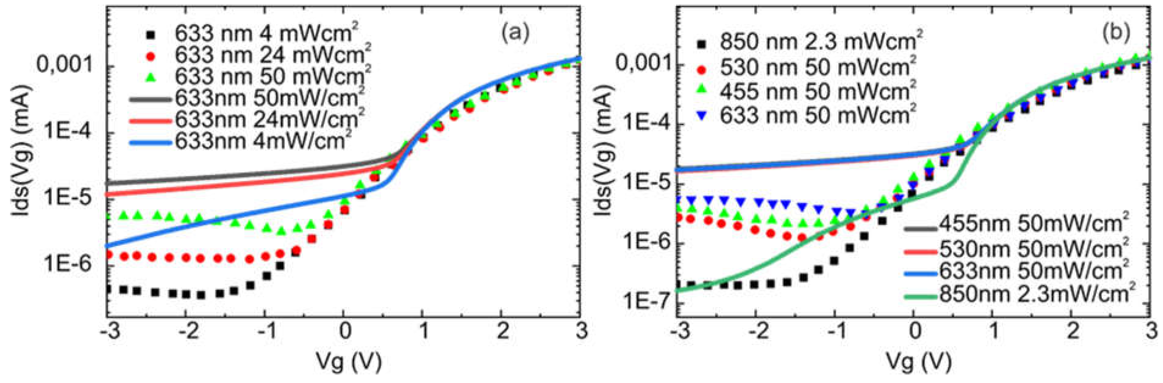
Despite efforts to account for a wide range of factors, such as trap density, donor impurities, Shockley Read Hall recombination mechanisms, and surface traps, discrepancies with experimental data persist, as illustrated in Figure 4. In some cases, the differences reach nearly a factor of five under certain combinations of voltage, wavelength, and TMDC thickness.
Additionally, uncertainties in optical absorption due to surface imperfections in quasi two-dimensional structures and at the TMDC dielectric interface significantly influence the results. Nonetheless, the calculated transfer characteristics qualitatively align with experimental data, particularly when varying optical power or illumination wavelength.
The spectral dependence for different thicknesses of MoS2 was subsequently modeled. The presented graphs reveal a relationship between the shape of the optical absorption curve and photocurrent, although the dependence on thickness is more straightforward. For example, at a wavelength of 700 nm, the absorption for thicknesses of 4 nm and 40 nm coincides (the lines in Figure (a) intersect). However, the photocurrent at this point differs by three orders of magnitude, which cannot be explained solely in terms of absorption.
This discrepancy arises from changes in the specific conductivity of the integrated channel. As the channel becomes wider with increasing thickness, the carrier concentration within it also increases. This phenomenon is consistent with the results presented in Supplementary 2, which provide further confirmation.
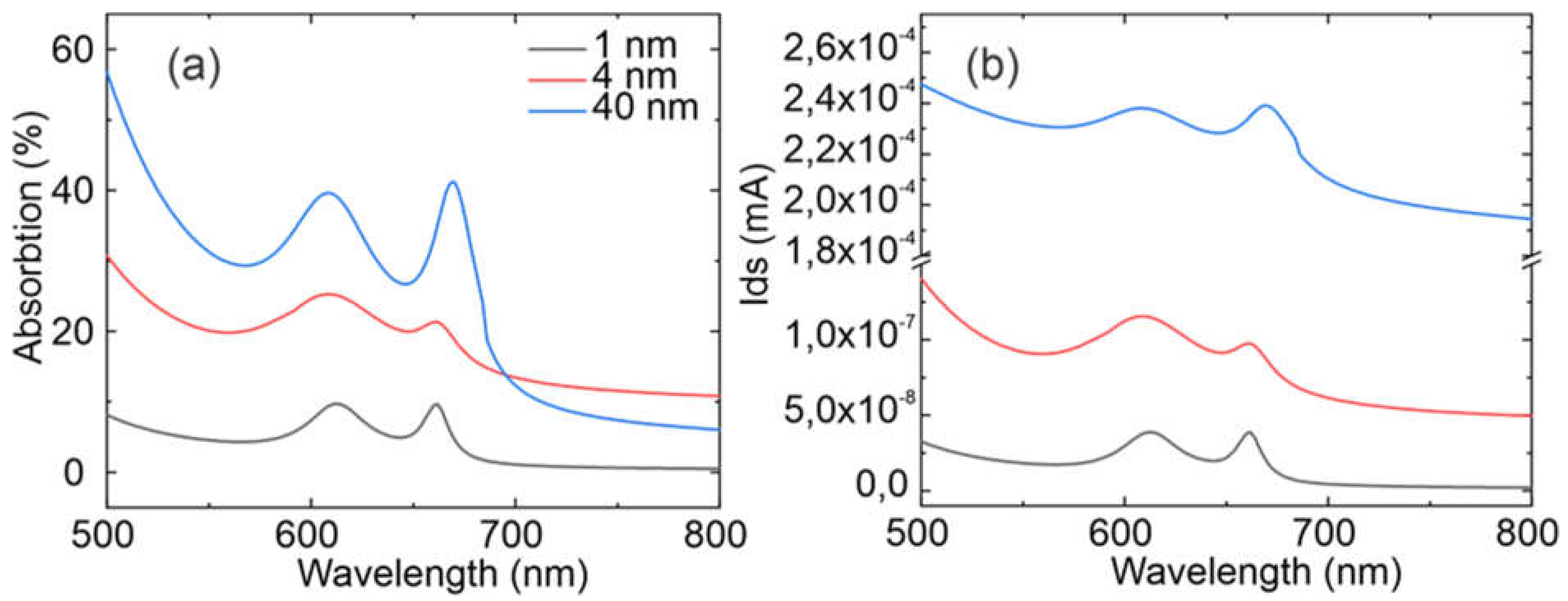
Figure 5.
(a) Spectral dependences of absorption and (b) photocurrent on optical wavelength for different MoS2 thicknesses.
Figure 5.
(a) Spectral dependences of absorption and (b) photocurrent on optical wavelength for different MoS2 thicknesses.
4. Conclusions
This study presents comprehensive modeling of a phototransistor based on quasi-two-dimensional transition metal dichalcogenides, integrating the simulation of optical absorption and semiconductor characteristics. The results demonstrate that the proposed approach successfully reproduces both dark and photocurrents under channel pinch-off conditions, highlighting the critical role of defect states (traps, impurities, and interfacial imperfections) in determining the resulting currents.
While the model may underestimate the dark current compared to experimental data, the qualitative correlation of the simulated characteristics with real measurements confirms its validity. It was observed that small variations in film thickness, doping level, and contact geometry can lead to significant deviations in device performance, consistent with published experimental results.
The obtained dependencies underscore the importance of detailed descriptions of defects and suggest the need for more precise consideration of interfacial effects and surface irregularities. Nevertheless, the modeling performed demonstrates the feasibility of designing and optimizing phototransistors based on 2D materials through the rational selection of structural and technological parameters, accelerating their integration into practical applications and emphasizing the importance of comprehensive physical modeling in modern nanoelectronics.
Supplementary Materials
The following supporting information can be downloaded at the website of this paper posted on Preprints.org, Supplementary 1 - Spectral dependence of optical absorption in a DPM film on its thickness, Supplementary 2 - Charge Carrier Concentration in the MoS2 Film, Supplementary 3 - Influence of MoS2 Thickness on Current, Supplementary 4 - Assessment of the Depletion Region in MoS2, Supplementary 5 - Dependence of Dark Current on MoS2 Characteristics.
Author Contributions
Conceptualization, S.D.L.; Validation, S.D.L.; writing—original draft preparation, S.D.L. and A.A.G.; writing—review and editing, S.D.L. and A.A.G.; visualization, A.A.G.; formal analysis, A.A.G. and S.D.L.; supervision, S.D.L.; Data curation, S.D.L. All authors have read and agreed to the published version of the manuscript.
Funding
The study was supported by the Russian Science Foundation [project number 24-79-10304] in the part of the semiconductor modeling of phototransistor characteristics and the Ministry of Science and Higher Education of the Russian Federation [project number FSFZ-2024-0047] in the part of the theoretical calculations of the optical components.
Conflicts of Interest
The authors declare no conflicts of interest.
References
- Cao, Linyou. "Two-dimensional transition-metal dichalcogenide materials: Toward an age of atomic-scale photonics." Mrs Bulletin 40.7 (2015): 592-599. [CrossRef]
- Upadhyay, Shrish Nath, Jena Akash Kumar Satrughna, and Srimanta Pakhira. "Recent advancements of two-dimensional transition metal dichalcogenides and their applications in electrocatalysis and energy storage." Emergent materials 4.4 (2021): 951-970. [CrossRef]
- Mir, Showkat Hassan, Vivek Kumar Yadav, and Jayant Kumar Singh. "Recent advances in the carrier mobility of two-dimensional materials: a theoretical perspective." ACS omega 5.24 (2020): 14203-14211. [CrossRef]
- Batool, Saima, et al. "Novel charm of 2D materials engineering in memristor: when electronics encounter layered morphology." Nanoscale Horizons 7.5 (2022): 480-507. [CrossRef]
- Zhao, Mingyue, et al. "Advances in two-dimensional materials for optoelectronics applications." Crystals 12.8 (2022): 1087. [CrossRef]
- Hassan, Jahan Zeb, et al. "2D material-based sensing devices: an update." Journal of Materials Chemistry A 11.12 (2023): 6016-6063. [CrossRef]
- Kuc, Agnieszka, Thomas Heine, and Andras Kis. "Electronic properties of transition-metal dichalcogenides." MRS bulletin 40.7 (2015): 577-584. [CrossRef]
- Dias, A. C., et al. "Band structure of monolayer transition-metal dichalcogenides and topological properties of their nanoribbons: Next-nearest-neighbor hopping." Physical Review B 98.7 (2018): 075202. [CrossRef]
- Liu, Anhan, et al. "The roadmap of 2D materials and devices toward chips." Nano-Micro Letters 16.1 (2024): 119. [CrossRef]
- Zavabeti, Ali, et al. "Two-dimensional materials in large-areas: synthesis, properties and applications." Nano-Micro Letters 12 (2020): 1-34. [CrossRef]
- Hossen, Moha Feroz, Sachin Shendokar, and Shyam Aravamudhan. "Defects and Defect Engineering of Two-Dimensional Transition Metal Dichalcogenide (2D TMDC) Materials." Nanomaterials 14.5 (2024): 410. [CrossRef]
- Liao, Wugang, et al. "Interface engineering of two-dimensional transition metal dichalcogenides towards next-generation electronic devices: recent advances and challenges." Nanoscale horizons 5.5 (2020): 787-807. [CrossRef]
- Tunga, Ashwin, et al. "Physics-based modeling and validation of 2-D Schottky barrier field-effect transistors." IEEE Transactions on Electron Devices 70.4 (2023): 2034-2041. [CrossRef]
- Jelver, Line, et al. "Schottky barrier lowering due to interface states in 2D heterophase devices." Nanoscale Advances 3.2 (2021): 567-574. [CrossRef]
- Taffelli, Alberto, et al. "MoS2 based photodetectors: a review." Sensors 21.8 (2021): 2758. [CrossRef]
- Ky, Dinh Le Cao, et al. "Friction characteristics of mechanically exfoliated and CVD-grown single-layer MoS 2." Friction 6 (2018): 395-406. [CrossRef]
- Choi, Woong, et al. "High-detectivity multilayer MoS2 phototransistors with spectral response from ultraviolet to infrared." Advanced materials 24.43 (2012): 5832. [CrossRef]
- He, Zhuoyang, HeeBong Yang, and Na Young Kim. "Device simulation study of multilayer MoS2 Schottky barrier field-effect transistors." Nanotechnology 36.3 (2024): 035701. [CrossRef]
- Buscema, Michele, et al. "Large and tunable photothermoelectric effect in single-layer MoS2." Nano letters 13.2 (2013): 358-363. [CrossRef]
- Furchi, Marco M., et al. "Mechanisms of photoconductivity in atomically thin MoS2." Nano letters 14.11 (2014): 6165-6170. [CrossRef]
- Song, Baokun, et al. "Layer-dependent dielectric function of wafer-scale 2D MoS2." Advanced Optical Materials 7.2 (2019): 1801250. [CrossRef]
- Guskov A.А., Bezvikonnyi N.V., Lavrov S.D. Kretschmann configuration as a method to enhance optical absorption in two-dimensional graphene-like semiconductors. Russian Technological Journal. 2024;12(4):96–105. [CrossRef]
- Lin, Ming-Wei, et al. "Thickness-dependent charge transport in few-layer MoS2 field-effect transistors." Nanotechnology 27.16 (2016): 165203. [CrossRef]
Figure 1.
Schematic representation of the phototransistor based on quasi-two-dimensional transition metal dichalcogenide film.
Figure 1.
Schematic representation of the phototransistor based on quasi-two-dimensional transition metal dichalcogenide film.
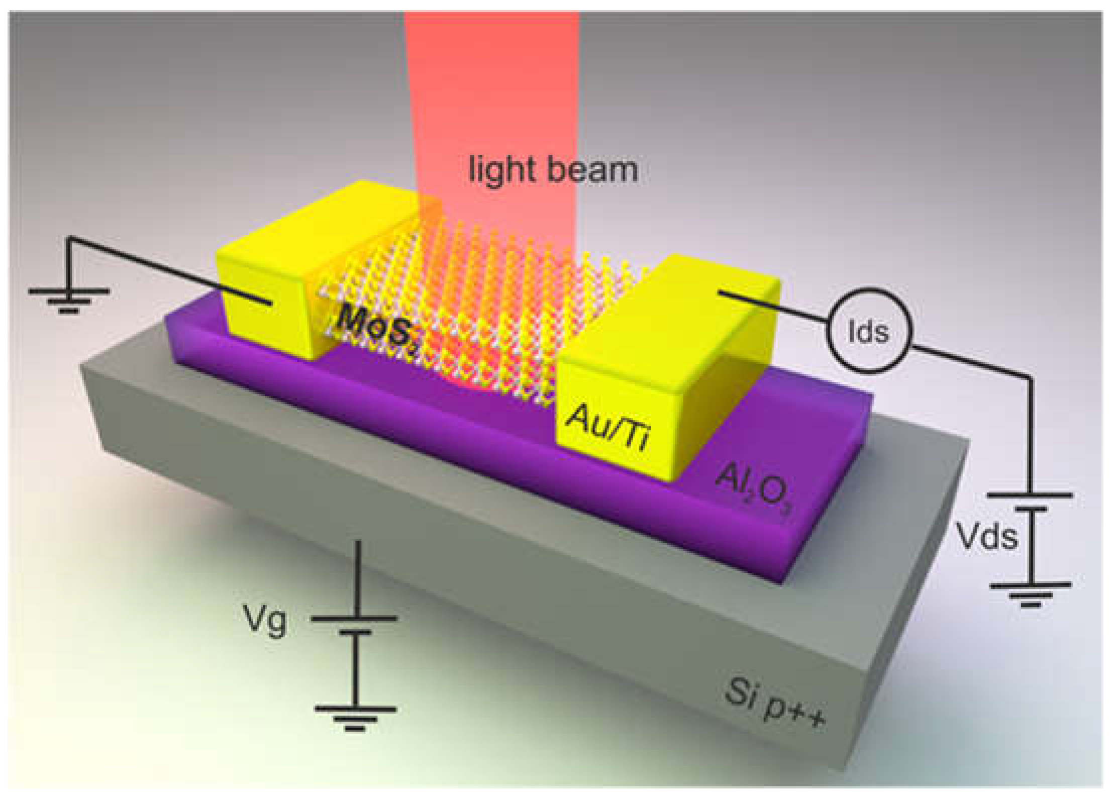
Figure 2.
Absorption spectra of MoS2 layers with varying thicknesses. The solid lines represent the calculated dependencies, while the points correspond to reference data from [17].
Figure 2.
Absorption spectra of MoS2 layers with varying thicknesses. The solid lines represent the calculated dependencies, while the points correspond to reference data from [17].
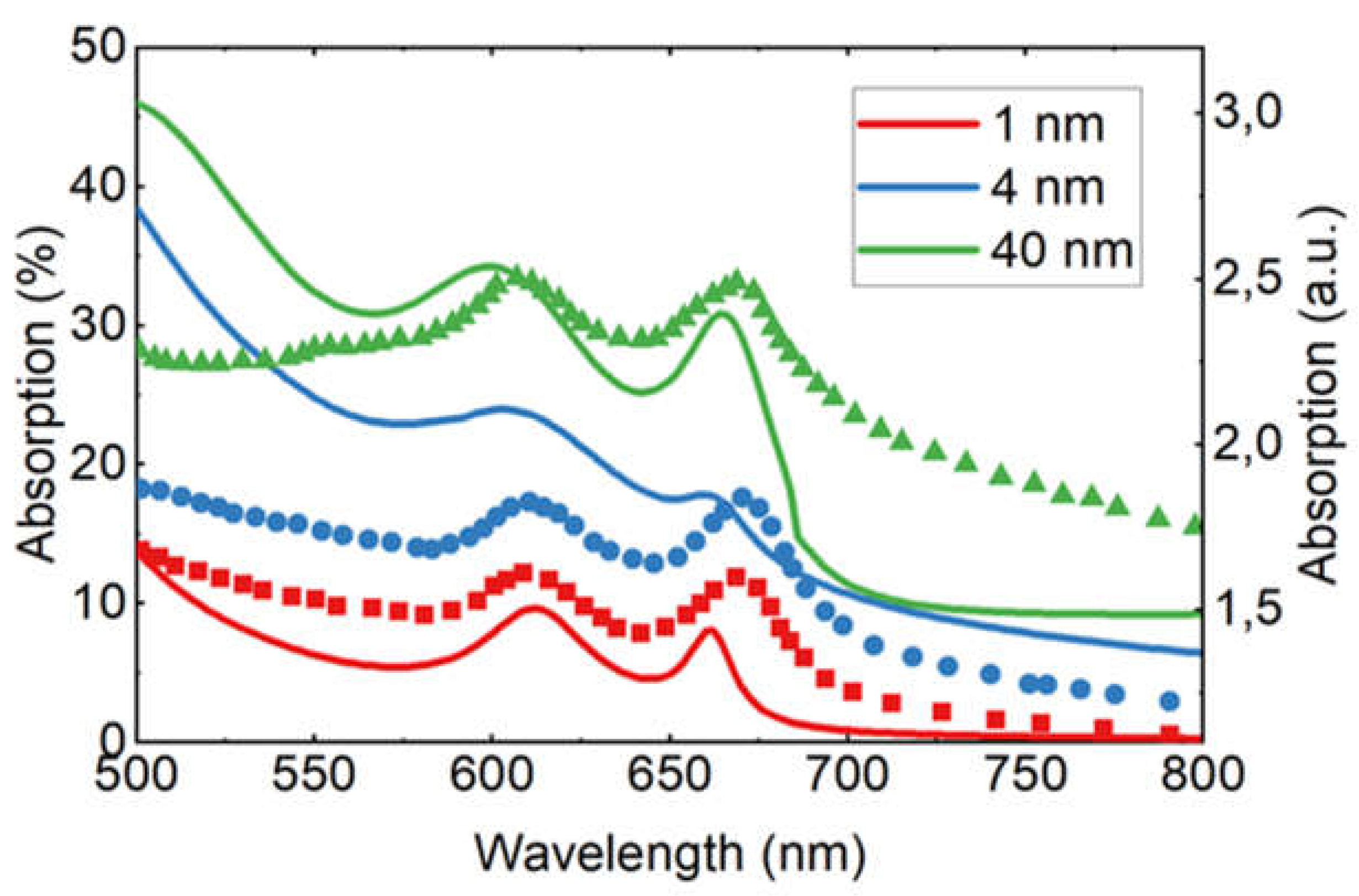
Figure 3.
Transfer characteristics for a quasi-2D MoS2 film with a thickness of 20 nm. Solid lines represent the calculated dependencies, while points correspond to reference data from [17].
Figure 3.
Transfer characteristics for a quasi-2D MoS2 film with a thickness of 20 nm. Solid lines represent the calculated dependencies, while points correspond to reference data from [17].
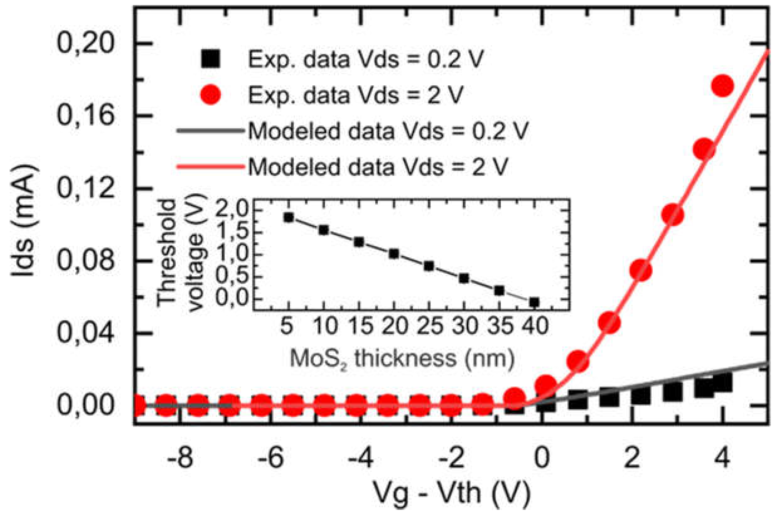
Figure 4.
Photocurrent dependence on gate voltage at a fixed wavelength of incident light (a) and at a fixed power of incident radiation (b). Solid lines represent the calculated dependencies, while points correspond to reference data from [17]. Vds = 1V.
Figure 4.
Photocurrent dependence on gate voltage at a fixed wavelength of incident light (a) and at a fixed power of incident radiation (b). Solid lines represent the calculated dependencies, while points correspond to reference data from [17]. Vds = 1V.
Disclaimer/Publisher’s Note: The statements, opinions and data contained in all publications are solely those of the individual author(s) and contributor(s) and not of MDPI and/or the editor(s). MDPI and/or the editor(s) disclaim responsibility for any injury to people or property resulting from any ideas, methods, instructions or products referred to in the content. |
© 2025 by the authors. Licensee MDPI, Basel, Switzerland. This article is an open access article distributed under the terms and conditions of the Creative Commons Attribution (CC BY) license (http://creativecommons.org/licenses/by/4.0/).
Copyright: This open access article is published under a Creative Commons CC BY 4.0 license, which permit the free download, distribution, and reuse, provided that the author and preprint are cited in any reuse.


