
Submitted:
09 December 2024
Posted:
10 December 2024
You are already at the latest version
Abstract
The thin-film lithium niobate platform, which is emerging as a promising photonic integration platform, currently lacks a polarization-insensitive grating coupler (GC), a crucial component for polarization-independent fiber interfaces. This limitation restricts its use in many applications such as polarization-insensitive modulation systems and polarization management. In this study, we propose a polarization-insensitive nonuniform GC, achieved by intersecting optimal TE- and TM-mode grating periods. Based on our simulation results, the proposed design delivers a coupling efficiency (CE) of 80% for TE and 78.5% for TM polarization, with a polarization-dependent loss of less than 0.14 dB at a wavelength of 1550 nm. The inserted gold layer, i.e., inside the substrate layer, boosts the CEs of the optimal TE- and TM-mode GC by about 50%, resulting in a highly efficient, polarization-insensitive solution. This advancement enables on-chip polarization diversity applications on the thin-film lithium niobate platform. We also investigate the fabrication and alignment tolerances of the proposed design to ensure robust performance under practical conditions.
Keywords:
Thin Film Lithium Niobate
; Optical Waveguide
; Grating Couplers
1. Introduction
The thin film Lithium niobate-on-insulator (TFLNOI) platform has recently attracted great attention because of its well-known advantages such as high integration density, strong optical confinement and complementary metal-oxide-semiconductor (CMOS) compatibility. Due to its exceptional features including a wide transparency range (0.35–5 μm) [1,2], high electro-optical and nonlinear coefficients [3,4,5], and useful properties like piezoelectricity [6], thermo-optical effects [7] and photorefractivity [8]. The TFLNOI platform is suitable for nonlinear and quantum optics [9]. However, the coupling of signals between optical fiber and submicron TFLNOI waveguides is challenging because of optical mode mismatch. Grating couplers (GCs) are commonly used for interfacing optical fibers with photonic integrated circuits due to their ease of fabrication, relaxed positional tolerance [9], and ability to facilitate multipoint wafer characterization [10]. They also eliminate the need for end-facet polishing [11], i.e., a significant challenge for TFLNOI, as the thin film can easily delaminate under the stress of grinding and polishing [12]. While GCs offer advantages like simple fiber coupling and flexible layout design, they increase the polarization dependency due to their inherent polarization-selective properties [1]. This limitation hinders their use in applications such as dual-polarization coherent modulators in telecommunications [13] and polarization controllers [14].
Polarization-dependent coupling results in large losses when interfacing a chip with optical fibers, as the polarization state in single-mode fibers (SMFs) can be unstable and unpredictable. Polarization-maintaining fibers (PMFs) offer improved stability by preserving the polarization state during transmission with some challenges. Therefore, it is crucial to engineer polarization-independent grating couplers (PIGCs) for both input and output light coupling. This characteristic enables efficient coupling of both transverse electric (TE) and transverse magnetic (TM) modes [15]. To overcome this limitation, significant research has been devoted to developing PIGCs. On silicon-on-insulator (SOI) substrates, two main approaches have emerged; one is the polarization-diversity GC, which can couple and split incoming light from a fiber into two waveguides with identical polarization [16,17], the other employs advanced techniques such as subwavelength gratings [18,19], two-way coupling [20], mixed gratings with Boolean operation [21], and inverse design methodologies to achieve polarization-independent one-dimensional (1D) GCs [19]. While many researchers have focused on the design and fabrication of TFLNOI-based GCs, their primary focus has been on improving coupling efficiency, with less attention given to the polarization-independency properties in their designs.
Simulation results on the hybrid silicon (Si) - TFLNOI grating coupler demonstrated a coupling efficiency of 51% for both TE and TM modes and a polarization-dependent loss (PDL) of 0.1 dB [22]. Although the device achieved over 70% CE for the TE mode, it exhibited relatively low efficiency for both TE and TM modes, with around 3 dB of loss and significant power coupling losses. A one-dimensional GC based on a metal layer on top of an x-cut TFLNOI substrate was demonstrated in [23]. The authors experimentally achieved CEs of -3.5 dB for TE and -3.7 dB for TM modes, with a PDL of 0.2 dB. A chirped grating coupler combined with a bottom metal layer was explored in [24]. The simulation results predicted CEs of 88.7% for TE and 67.9% for TM. Experimentally, CEs of 72% for TE and 62% for TM were achieved at 1.571 μm, showing a significant discrepancy between simulation and experimental results due to the challenge of direct etching of LN. The design was unable to achieve polarization independence. In contrast, designs that employed direct etching on dielectric materials such as Si or SiN on top of the LN waveguide exhibited better consistency between experimental and simulation results [25,26,27].
In this work, we use the easy etching benefits of Si material on top of the TFLNOI platform and explore a nonuniform PIGC using the intersection method. This approach achieves CEs of around 80% and PDL of 0.2 dB, while ensuring the fabrication process remains accessible using standard lithography and Si dry etching techniques [27]. First, the single-polarization GC structure for TE and TM modes are optimized to achieve high CEs of over 90% for each. Then, by applying mathematical intersection on the two optimized GC structures, we create a nonuniform PIGC that efficiently supports both polarizations. The combination of high efficiency, low loss, and straightforward fabrication highlights the potential of this design for a wide range of applications, including optical communication and quantum photonics.
2. Operating Principles of GC and Device Structure
A GC is a periodic structure used in integrated photonics to couple light between a waveguide platform and optical fiber, serving as an input/output device interface. The proposed design features a Si-GC on the SiO2/LN/SiO2/Au films, as shown in Figure 1. The key design parameters include the grating period (Λ), the fill factor (ff), i.e., the ratio of the groove width to the grating period, the thickness of the Si-GC (HSi), the LN waveguide thickness (HLN), the SiO2 layer thickness (HSiO2) located between the Si and LN waveguide layers; and the buried SiO2 film thickness (HBOX) underneath both the LN waveguide and SiO2 cladding layer (Hclad). The tilt angle of the single-mode fiber is denoted by θ. When the wavelength satisfies the Bragg condition, light scatters upwards and is efficiently coupled into the optical fiber through the silicon grating structure [28]. In our simulations, the refractive indices used for LN, Si, and SiO2 at a wavelength of 1550 nm are 2.22, 3.48, and 1.44, respectively [27]. Additionally, an SMF with a core diameter of 8.2 μm and a cladding diameter of 100 μm is used to collect the diffracted light. The surface grating has a length of 15 um and a width of 8.5 um. The monitor used to calculate the CE is positioned at (4.5μm, 3μm, 0) in the xyz-coordinate system as shown in Figure 1 (a).
To validate our simulation models, we first replicate the results reported in a previous study on a 2D PIGC on SOI [29]. This comparison between experimental and simulations demonstrates the accuracy of our simulation method. The design and optimization of the proposed grating coupler were conducted using the 2D finite-difference time-domain (FDTD) method. While 3D FDTD simulations account for out-of-plane effects and offer a more comprehensive analysis, 2D FDTD was chosen for this study due to its significantly reduced computational time and memory requirements. This is particularly beneficial for iterative optimization processes, where numerous simulations are needed to refine the design. Previous studies have shown that the coupling efficiency results obtained from 2D FDTD simulations closely match those from full 3D FDTD simulations for similar grating coupler designs [30]. This validates the use of 2D FDTD as an efficient and reliable method for analyzing grating couplers during the design phase.
In this paper, we simulate light coupling from a grating coupler to a single-mode. A region of 25 μm in the x-direction and 6.3 μm in the y-direction was used in our 2D FDTD simulations. The origin point used in our simulation is located at the beginning of the Si grating in x-direction, center of the Si grating in the z-direction, and top of the Si grating in the y-direction as approximately illustrated in Figure 1 (a). To ensure that the fiber effectively collects the upward optical power while minimizing high-order diffraction, we use the diffraction order m = +1 [31]. This choice maximizes both the bandwidth and coupling efficiency. In contrast, using a higher order, such as m = +2, can result in light being directed in undesirable directions due to scattering at steeper angles. To achieve an optimal efficiency-bandwidth product and a uniform grating for both TE and TM modes, we investigate several factors: the ff, Λ, HSi, HSiO2, HLN, and θ, as detailed later in Section 3. The iterative optimization process employs a For loop that sweeps through design parameters, adjusting each one by a small step size of 1 nm in each iteration. The loop iteratively refines the parameters until the optimal dimensions are reached, at which point the iteration concludes. We fixed the Hclad and the HBOX at 2 µm to comply with the fabrication standards outlined in [27].
3. Results and Discussion
3.1. Optimization of Single Polarization GCs
First, we optimize the single polarization GC structures. This optimization process focuses on key parameters, including the grating period and the fiber angle, to achieve the maximum CE for both TE and TM polarizations. The results of this optimization are illustrated in Figure 2. The variation of CE at a wavelength of 1.55 μm as a function of grating period and fiber angle are presented in Figure 2 (a) and (c), respectively, while the relationship between CE and wavelength for the optimum grating periods is demonstrated in Figure 2 (b). The parameters yielding to the highest CE for both TE and TM modes are listed in Table 1. The simulation is conducted using the FDTD method with perfectly matched layer (PML) boundary conditions and a mesh size of 5 nm [32]. Furthermore, the total grating length is 15 μm, from zero to 15 μm in the X-axis for TE and TM designs. However, the number of gratings used for TE design is 18 and 17 for TM design. As shown in Figure 2 (a) and (b), the optimal single-mode CEs of 85.5% for TE mode and 89% for TM mode are achieved with a period of 0.810 μm and 0.870 μm, respectively. It is observed that a 10 nm deviation in the grating period reduces the CE by 17% at 1.55 μm, while the peak experiences a redshift of 10 nm, as indicated in Figure 2 (a).
The CEs are calculated with varying fiber angles from 7 to 12 degrees, as shown in Figure 2 (c). For the TE design, an optimal CE of 85.5% at 1.55 μm was achieved with a fiber angle of 9 degrees. For the TM design, the optimal fiber angle was 12 degrees, with a CE of 89% at 1.55 μm. It is observed that an angular deviation of ±1 degree introduces an additional loss of around 2% in the CEs, demonstrating that the optimized structures can accommodate this misalignment tolerance. The TM mode study exhibited similar behavior to the TE mode regarding the effects of parameter deviations on coupling efficiency and additional loss. The key difference between the two designs lies in the values of the period (Figure 2 (a)) and fiber angle (Figure 2 (c)), as these parameters must be optimized to satisfy the Bragg conditions for the GC [33].
The coupling performance of the optimized TE and TM designs is visualized through their calculated field profiles, as shown in Figure 3 (a). These profiles clearly demonstrate the high coupling efficiencies achieved for both polarizations. To enhance the CE by redirecting power upward to the LN waveguide [34], a thin layer of gold (Au) is positioned below the buried SiO2 film as a reflector, and the simulated CEs for structures with and without the metal reflector for both TE and TM polarizations are depicted in Figure 3 (b) and (c), respectively. It is observed that for a TE mode single-polarization device on a 600 nm TFLNOI platform with a uniform grating design and a bottom reflector, the optimum CE is 85.5% at 1.55 μm, with a 3dB bandwidth of 90 nm. In contrast, without the metal layer, the CE drops to approximately 48%, as shown in Figure 3 (b). For a TM mode single-polarization design on the same 600 nm TFLNOI platform with a uniform grating design and a bottom reflector layer, the optimum CE is 89% at 1.55 μm, with a 3dB bandwidth of 120 nm. The CE is 75% without the metal layer, as shown in Figure 3 (c). The upward radiated powers depicted in Figure 3 (b) and (c) refer to the total power emitted in the upward direction. A portion of this power couples into the single mode fiber, which is referred to as CE, while the other portion is diffracted upward.
3.2. Polarization-Independent Grating Coupler Design Analysis
As shown in Figure 3 (d), we use the intersection of two optimum grating periods to create nonuniform gratings [29]. The primary goal of designing a PIGC is to ensure that the effective refractive indices for TE (Neff,TE) and TM (Neff _TM) are nearly equal [35]. This is typically achieved by modifying the grating parameters like period, etch depth, and fill factor [36]. Therefore, we modify the grating period by making the combination intersection method between two optimal grating periods to achieve a match for the effective index TE and TM values of the single-mode waveguide [29]. Using this intersection approach, we create a nonuniform PIGC. The effective index for the final design is calculated using the FDTD method, resulting in values of 1.93 for TE and 1.91 for TM, which are closely matched, providing the intended goal of polarization-independent coupling. The GC obtained by applying the intersection method on the optimum TE and TM designs demonstrates CEs of 81% for TE and 78% for TM with a fiber tilt angle of 10 degrees at a wavelength of 1.55 μm, as shown in Figure 4 (a). Table 2 presents a comparison of our work with other literature, illustrating that our results outperform those of previous studies in terms of CEs and polarization-dependent loss (PDL) in polarization-insensitive capabilities.
To investigate the tolerance of the final PIGC design to misalignment in terms of both angle and position, the CEs and PDL as functions of fiber angle and fiber position were calculated, and the results are demonstrated in Figure 4 (b), (c), and (d), respectively. As shown in Figure 4 (b), the optimum coupling angle is achieved by sweeping the fiber angle from 7 to 12 degrees, demonstrating an increase in CE for both TE and TM modes, alongside a reduction in PDL until 10 degrees. Beyond this point, the CE gradually decreases. The results illustrate that a 1-degree coupling misalignment relative to the optimal value of 10 degrees leads to a 10 to 20% reduction in CEs and approximately a threefold increase in PDL, which could undermine the primary goal of polarization insensitivity. Additionally, the optimal fiber position was set using the diffraction beam law [37], at 4.5 μm in the X direction and 3 μm in the Y direction. As shown in Figure 4 (c) and (d), the origin point in this figure represents the optimal values of 4.5 μm on the x-axis and 3 μm on the y-axis. Positive mispositioning (+0.5 μm) in the X and Y directions of the optical fiber relative to the optimal values leads to a reduction in CEs, while negative mispositioning (-0.5 μm) results in a greater decrease in CEs, particularly for negative mispositioning in the Y direction. This demonstrates that the device is more tolerant of positive mispositioning than negative mispositioning. However, mispositioning (±0.5 μm) of the optical fiber affects PDL differently in the X and Y directions. Misalignment along the X-axis reduces the PDL, as shown in Figure 4 (d), while misalignment along the Y-axis within the same range significantly does not change the PDL. Since the grating region begins from zero in the X-axis, the optimum location of optical fiber in the axis is 4.5 μm. Therefore, to maintain the polarization insensitivity of the proposed PIGC, accurate alignment in the Y direction is more critical than in the X direction.
To estimate the tolerance of our proposed PIGC to fabrication errors, we investigate the impact of variations in key geometrical parameters on the CEs and PDL. The calculated CEs and PDL as functions of grating width, etch depth, buffer, and waveguide thickness are presented in Figure 5. Throughout these simulations, varying the thickness of the Au layer at the bottom reflector from 50 nm to 100 nm resulted in relatively unchanged CEs for both TE and TM modes. Additionally, the thicknesses of the SiO2 layer, Hclad, and HBOX were fixed at 2 μm to meet fabrication standards [27]. Figure 5 (a) shows that varying the widths of all grating grooves by ±10 nm in the X direction, while keeping the center points unchanged, introduces an additional loss in CE for both TE and TM modes of less than 20% and increases the PDL to nearly -2 dB.
Therefore, the groove width fabrication error should be kept below ±5 nm, which is achievable using e-beam lithography [38].
For the etch depth fabrication error estimation, we varied the thickness of all grooves by ±50 nm in the y direction, and the results are demonstrated in Figure 5 (b). The results show that an etch depth fabrication tolerance of ±10 nm has a negligible impact on CEs and PDL. As shown in Figure 5 (c) and (d), variations of HLN and HSiO2 within the range of ±10 nm add an additional loss of 0.21 dB and 0.12 dB in PDL, respectively, with negligible impact on CEs. These findings indicate that the proposed PIGC design exhibits a good tolerance to fabrication errors, ensuring reliable performance in practical applications. The advantages of the proposed design include higher flexibility and the possibility of integration of different materials, and a more stable fabrication process in the TFLNOI platform [27]. We believe the fabrication of such a device will have a good match of experimental and simulation results similar to those reported in the literature [25,26,27].
4. Conclusions
In conclusion, we demonstrate a grating coupler based on a silicon grating coupler on the top of the LN thin film waveguide for high single-polarization and polarization-independent GCs. By using the intersection method for optimal single grating periods of TE and TM designs, the nonuniform PIGC is formed with PDL of 0.2dB and CEs of 80/78% for TE/TM respectively. The proposed GC archives CEs of 89/85.5% with 3 dB bandwidth 72 /120 nm at 1.55 μm for TE and TM, respectively. We discuss the alignment and fabrication tolerance for the PIGC. This work has predictions for future TFLNOI-based devices that can operate effectively regardless of polarization for varies applications in which polarization insensitive is required
Author Contributions
Conceptualization, A. S. and M. K.; methodology, A. S. and M. K; software, A. S. and M. K; validation, A. S. and M. K; formal analysis, A. S. and M. K.; writing—original draft preparation, A. S; writing—review and editing, M. K.; supervision, C.X. All authors have read and agreed to the published version of the manuscript.
Funding
This research was funded by McMaster University.
Data Availability Statement
The raw data supporting the conclusions of this article will be made available by the authors on request.
Conflicts of Interest
The authors declare no conflicts of interest.
References
- Wang, C.; et al. , Monolithic lithium niobate photonic circuits for Kerr frequency comb generation and modulation. Nature communications 2019, 10, 978. [Google Scholar] [CrossRef] [PubMed]
- Zhang, M.; et al. , Broadband electro-optic frequency comb generation in a lithium niobate microring resonator. Nature 2019, 568, 373–377. [Google Scholar] [CrossRef] [PubMed]
- Lin, J.; et al. , Advances in on-chip photonic devices based on lithium niobate on insulator. Photonics Research 2020, 8, 1910–1936. [Google Scholar] [CrossRef]
- Poberaj, G.; et al. , Lithium niobate on insulator (LNOI) for micro-photonic devices. Laser & photonics reviews 2012, 6, 488–503. [Google Scholar]
- Boes, A.; et al. , Status and potential of lithium niobate on insulator (LNOI) for photonic integrated circuits. Laser & Photonics Reviews 2018, 12, 1700256. [Google Scholar]
- Jiang, W.; et al. , Lithium niobate piezo-optomechanical crystals. Optica 2019, 6, 845–853. [Google Scholar] [CrossRef]
- Wang, J.; et al. , Thermo-optic effects in on-chip lithium niobate microdisk resonators. Optics Express 2016, 24, 21869–21879. [Google Scholar] [CrossRef]
- Jiang, H.; et al. , Fast response of photorefraction in lithium niobate microresonators. Optics letters 2017, 42, 3267–3270. [Google Scholar] [CrossRef]
- Agrell, E.; et al. , Roadmap of optical communications. Journal of optics 2016, 18, 063002. [Google Scholar] [CrossRef]
- Mahmoud, M., S. Ghosh, and G. Piazza. Lithium niobate on insulator (LNOI) grating couplers. in CLEO: Science and Innovations. 2015. Optica Publishing Group.
- Snyder, B. and P. O'Brien, Packaging process for grating-coupled silicon photonic waveguides using angle-polished fibers. IEEE Transactions on Components, Packaging and Manufacturing Technology 2013, 3, 954–959. [Google Scholar]
- Baghsiahi, H.; et al. , Optical waveguide end facet roughness and optical coupling loss. Journal of Lightwave Technology 2013, 31, 2959–2968. [Google Scholar] [CrossRef]
- Wang, Z.; et al. , Silicon–lithium niobate hybrid intensity and coherent modulators using a periodic capacitively loaded traveling-wave electrode. Acs Photonics 2022, 9, 2668–2675. [Google Scholar] [CrossRef]
- Lin, Z.; et al. , High-performance polarization management devices based on thin-film lithium niobate. Light: Science & Applications 2022, 11, 93. [Google Scholar]
- Lin, C.-C.; et al. , Design of a Completely Vertical, Polarization-Independent Two-Dimensional Grating Coupler with High Coupling Efficiency. Sensors 2023, 23, 4662. [Google Scholar] [CrossRef]
- Taillaert, D.; et al. , A compact two-dimensional grating coupler used as a polarization splitter. IEEE Photonics Technology Letters 2003, 15, 1249–1251. [Google Scholar] [CrossRef]
- Chen, B.; et al. , Two-dimensional grating coupler on silicon with a high coupling efficiency and a low polarization-dependent loss. Optics Express 2020, 28, 4001–4009. [Google Scholar] [CrossRef]
- Cheng, Z. and H.K. Tsang, Experimental demonstration of polarization-insensitive air-cladding grating couplers for silicon-on-insulator waveguides. Optics Letters 2014, 39, 2206–2209. [Google Scholar] [CrossRef]
- Hao, T.; et al. , Dual-band polarization-independent subwavelength grating coupler for wavelength demultiplexing. IEEE Photonics Technology Letters 2020, 32, 1163–1166. [Google Scholar] [CrossRef]
- Xie, H.; et al. , Ultra-compact subwavelength-grating-assisted polarization-independent directional coupler. IEEE Photonics Technology Letters 2019, 31, 1538–1541. [Google Scholar] [CrossRef]
- Wüster, J.; et al. , Nano-imprinted subwavelength gratings as polarizing beamsplitters. Journal of the European Optical Society-Rapid Publications 2021, 17, 4. [Google Scholar] [CrossRef]
- Ma, X.; et al. , Polarization-independent one-dimensional grating coupler design on hybrid silicon/LNOI platform. Optics Express 2020, 28, 17113–17121. [Google Scholar] [CrossRef] [PubMed]
- Chen, B.; et al. , One-dimensional grating coupler on lithium-niobate-on-insulator for high-efficiency and polarization-independent coupling. Optics Letters 2023, 48, 1434–1437. [Google Scholar] [CrossRef] [PubMed]
- Kang, S.; et al. , High-efficiency chirped grating couplers on lithium niobate on insulator. Optics Letters 2020, 45, 6651–6654. [Google Scholar] [CrossRef] [PubMed]
- Zhou, X.; et al. , High coupling efficiency waveguide grating couplers on lithium niobate. Optics Letters 2023, 48, 3267–3270. [Google Scholar] [CrossRef]
- Han, X.; et al. , Single-step etched grating couplers for silicon nitride loaded lithium niobate on insulator platform. Apl Photonics 2021, 6. [Google Scholar] [CrossRef]
- Jian, J.; et al. , High-efficiency hybrid amorphous silicon grating couplers for sub-micron-sized lithium niobate waveguides. Optics express 2018, 26, 29651–29658. [Google Scholar] [CrossRef]
- Chrostowski, L. and M. Hochberg, Silicon Photonics Design. 2015: Cambridge University Press.
- Song, J.H.; et al. , Polarization-independent nonuniform grating couplers on silicon-on-insulator. Optics letters 2015, 40, 3941–3944. [Google Scholar] [CrossRef]
- Chrostowski, L. and M. Hochberg, Silicon photonics design: From devices to systems. 2015: Cambridge University Press.
- Statkiewicz-Barabach, G.; et al. , Fabrication of multiple Bragg gratings in microstructured polymer fibers using a phase mask with several diffraction orders. Optics Express 2013, 21, 8521–8534. [Google Scholar] [CrossRef]
- Gedney, S.D. , Introduction to the finite-difference time-domain (FDTD) method for electromagnetics. Vol. 27. 2011: Morgan & Claypool Publishers.
- Othonos, A. , Fiber bragg gratings. Review of scientific instruments 1997, 68, 4309–4341. [Google Scholar] [CrossRef]
- Zaoui, W.S.; et al. , Cost-effective CMOS-compatible grating couplers with backside metal mirror and 69% coupling efficiency. Optics express 2012, 20, B238–B243. [Google Scholar] [CrossRef]
- Chen, X. and H.K. Tsang, Polarization-independent grating couplers for silicon-on-insulator nanophotonic waveguides. Optics letters 2011, 36, 796–798. [Google Scholar] [CrossRef] [PubMed]
- Benedikovic, D.; et al. , High-efficiency single etch step apodized surface grating coupler using subwavelength structure. Laser & Photonics Reviews 2014, 8, L93–L97. [Google Scholar]
- Reinisch, R.; et al. , Coupled-mode formalism and linear theory of diffraction for a simplified analysis of second harmonic generation at grating couplers. Optics communications, 1994, 112, 339–348. [Google Scholar] [CrossRef]
- Zeitner, U.D.; et al. , High performance diffraction gratings made by e-beam lithography. Applied Physics A 2012, 109, 789–796. [Google Scholar] [CrossRef]
Figure 1.
Schematics of grating coupler on the hybrid LNOI platform with silicon on top: (a) 3D sketch, and (b) side view.
Figure 1.
Schematics of grating coupler on the hybrid LNOI platform with silicon on top: (a) 3D sketch, and (b) side view.
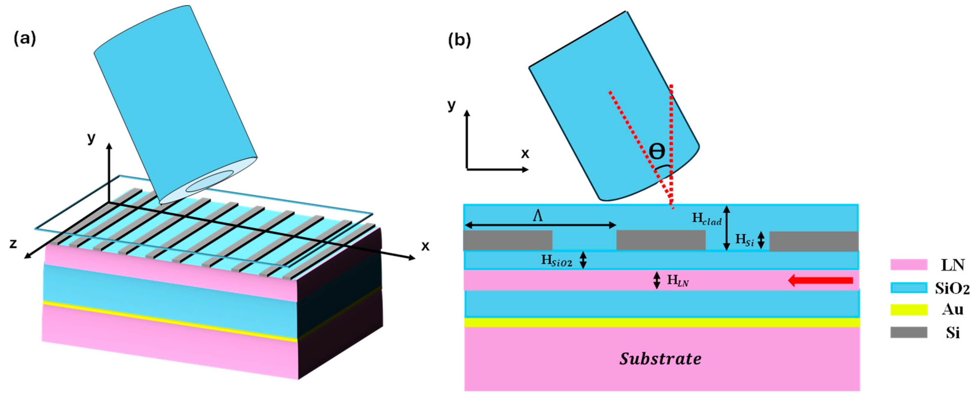
Figure 2.
(a) The coupling efficiencies and peak wavelength calculated for different periods for TE mode. (b) The coupling efficiencies for optimal periods TE and TM mode. (c) The coupling efficiencies calculated for different fiber angles for TE and TM modes.
Figure 2.
(a) The coupling efficiencies and peak wavelength calculated for different periods for TE mode. (b) The coupling efficiencies for optimal periods TE and TM mode. (c) The coupling efficiencies calculated for different fiber angles for TE and TM modes.
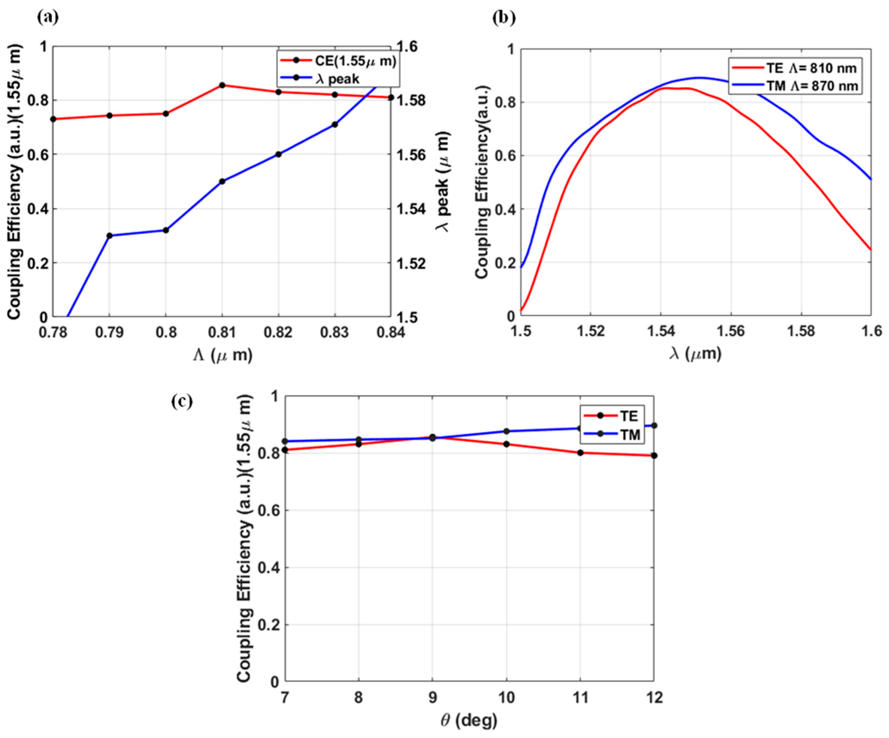
Figure 3.
(a) The field profiles of uniform grating coupler designs. CEs and total power calculated for the proposed grating couplers design for: (b) TE mode, (c) TM mode. (d) Schematic diagram shows the intersection of TE and TM grating periods to create a nonuniform grating period.
Figure 3.
(a) The field profiles of uniform grating coupler designs. CEs and total power calculated for the proposed grating couplers design for: (b) TE mode, (c) TM mode. (d) Schematic diagram shows the intersection of TE and TM grating periods to create a nonuniform grating period.
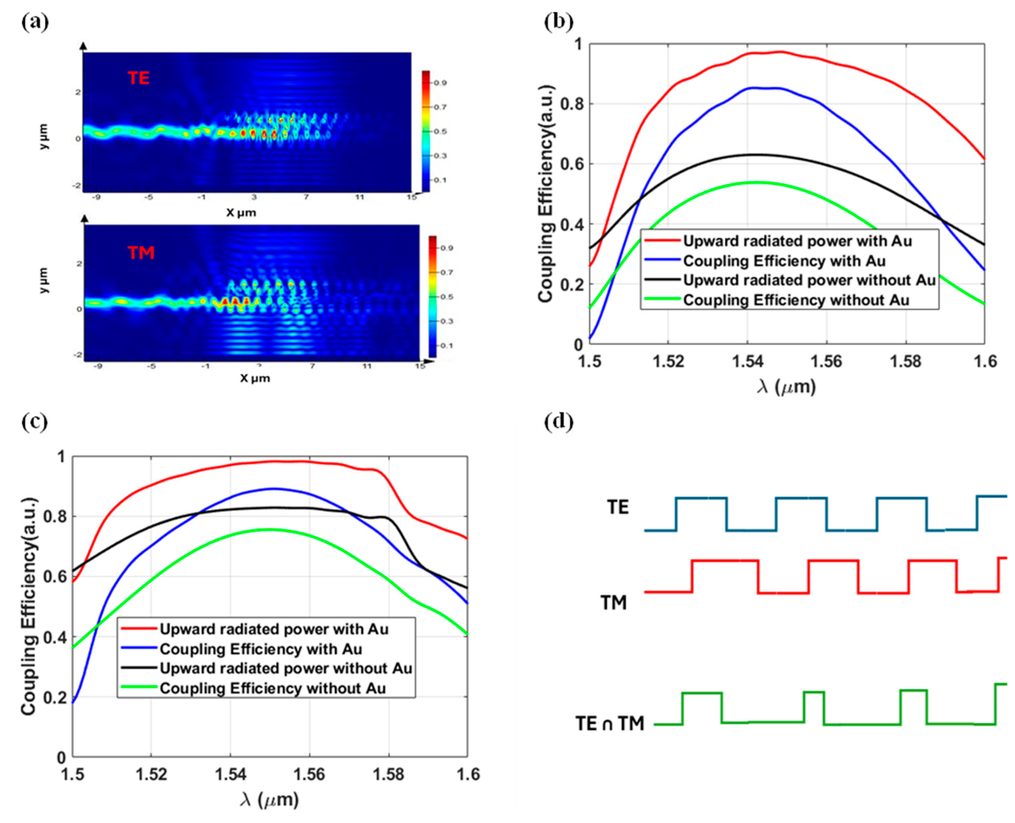
Figure 4.
(a) The calculated CE and PDL vs wavelength. (b) The calculated CE and PDL vs fiber angle. (c) The calculated CE and PDL vs fiber position (c) for displacement Δx from the optimal X position (4.5 μm) and (d) displacement Δy from the optimal Y position (3.0 μm).
Figure 4.
(a) The calculated CE and PDL vs wavelength. (b) The calculated CE and PDL vs fiber angle. (c) The calculated CE and PDL vs fiber position (c) for displacement Δx from the optimal X position (4.5 μm) and (d) displacement Δy from the optimal Y position (3.0 μm).
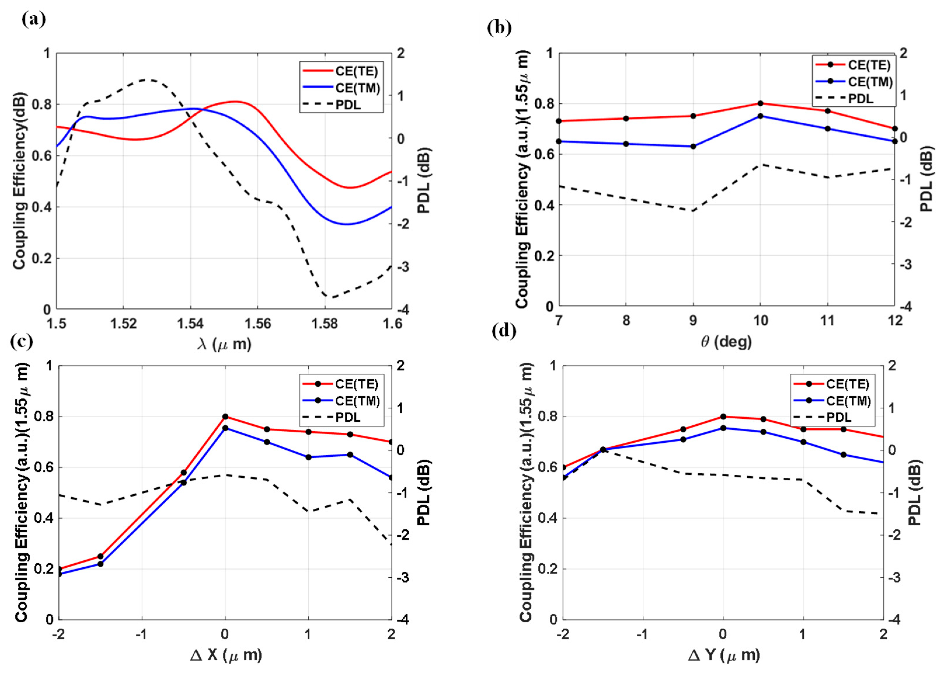
Figure 5.
The coupling efficiencies and PDL as a function of (a) the groove width of each uniform grating used in the nonuniform grating coupler; (b) the etch depth for nonuniform grating coupler; (c) the change in the HBox for the nonuniform grating coupler; (d) the change in buffer thickness (HSiO2) for nonuniform grating coupler.
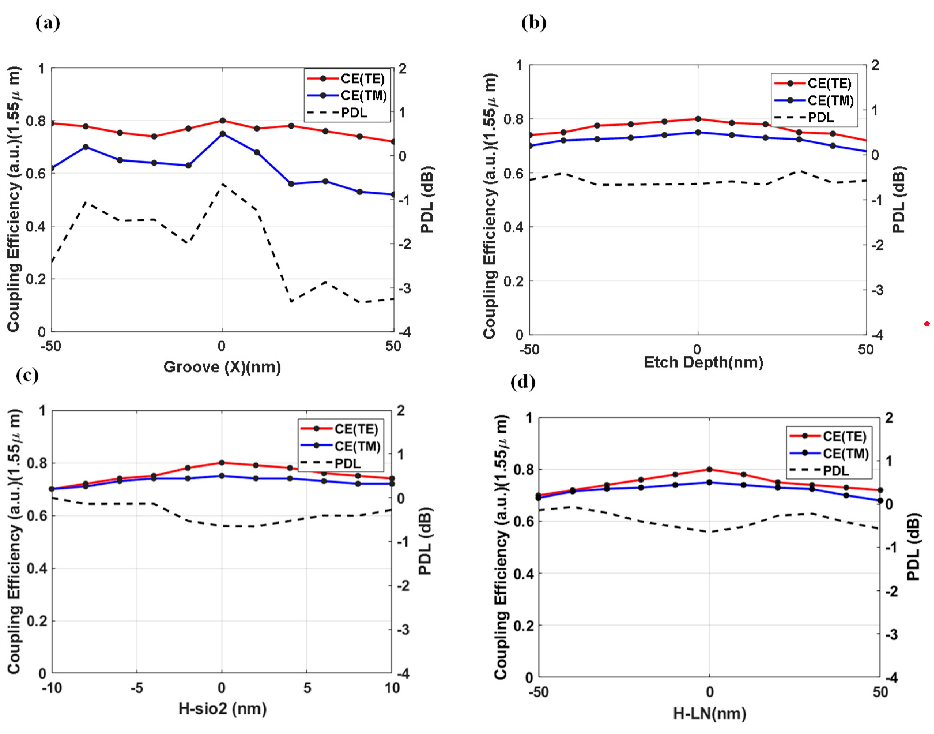

Table 1.
Coupling efficiencies and parameter values of the optimized LNOI grating couplers.
| Λ [nm] | Etch depth [nm] | Fill Factor | θ deg | CE | |
|---|---|---|---|---|---|
| TE | 810 | 340 | 0.54 | 9 | 85.5% |
| TM | 870 | 340 | 0.54 | 12 | 89% |
Table 2.
Coupling efficiencies and parameter values of the optimized TFLNOI grating couplers.
| Ref | LN height [nm] | Metal layer thickness [nm] | Simulation | Experiment | PDL [dB] | Notes | ||
|---|---|---|---|---|---|---|---|---|
| CE | 3dB Bandwidth [nm] TE/TM |
CE | 3dB Bandwidth [nm] TE/TM |
|||||
| This work | 600 | 100 | 85.5/89% | 70/120 | NA | NA | 0.14 | Hybrid GC Si on LNOI platform |
| [22] | 600 | NA | 51/51% | 83/106 | NA | NA | 0.1 | Hybrid GC Si on LNOI platform |
| [23] | 400 | 50 | -3.5/-3.7dB | 40 | 3.57/ 4 dB | 40 | 0.69 | Uniform GC Au layer on x-cur LNOI |
| [24] | 500 | 100 | 88.7/68 % | 38 | 72/62% | 38 | NA | Chirp GC on z-cut LNOI with an Au layer |
Disclaimer/Publisher’s Note: The statements, opinions and data contained in all publications are solely those of the individual author(s) and contributor(s) and not of MDPI and/or the editor(s). MDPI and/or the editor(s) disclaim responsibility for any injury to people or property resulting from any ideas, methods, instructions or products referred to in the content. |
© 2024 by the authors. Licensee MDPI, Basel, Switzerland. This article is an open access article distributed under the terms and conditions of the Creative Commons Attribution (CC BY) license (https://creativecommons.org/licenses/by/4.0/).
Copyright: This open access article is published under a Creative Commons CC BY 4.0 license, which permit the free download, distribution, and reuse, provided that the author and preprint are cited in any reuse.


