Submitted:
09 December 2024
Posted:
09 December 2024
You are already at the latest version
Abstract
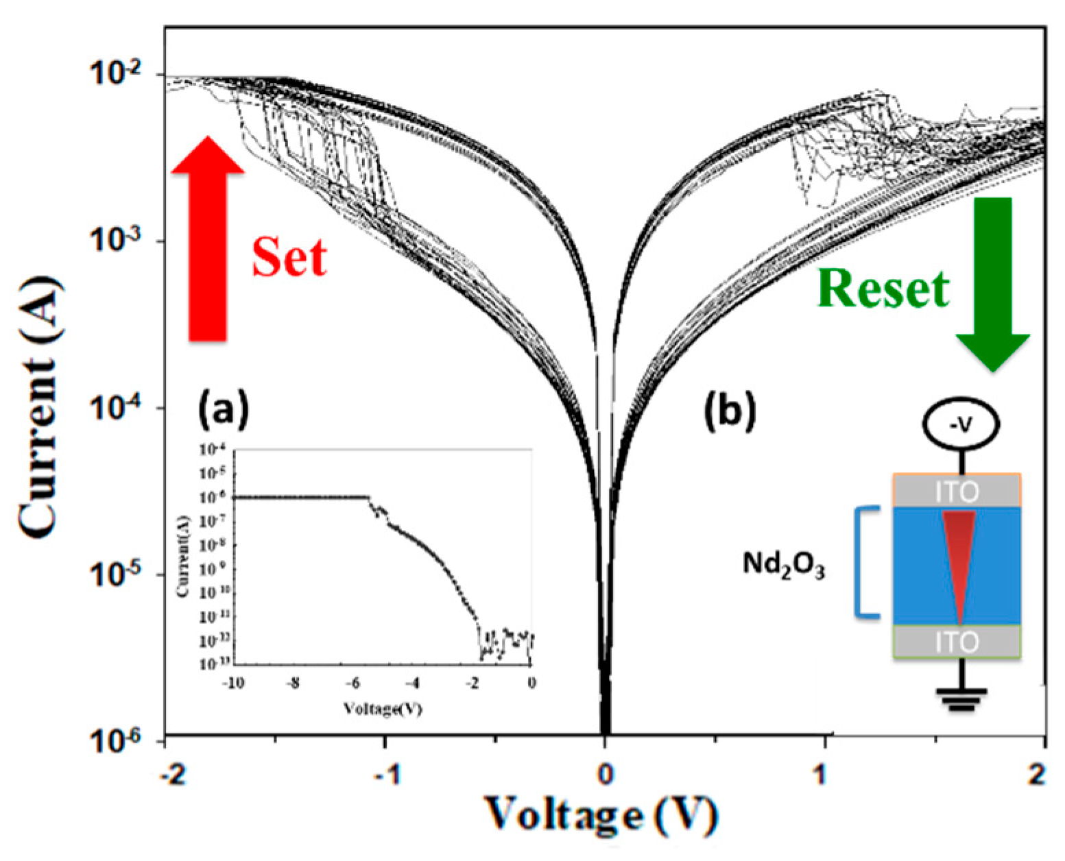
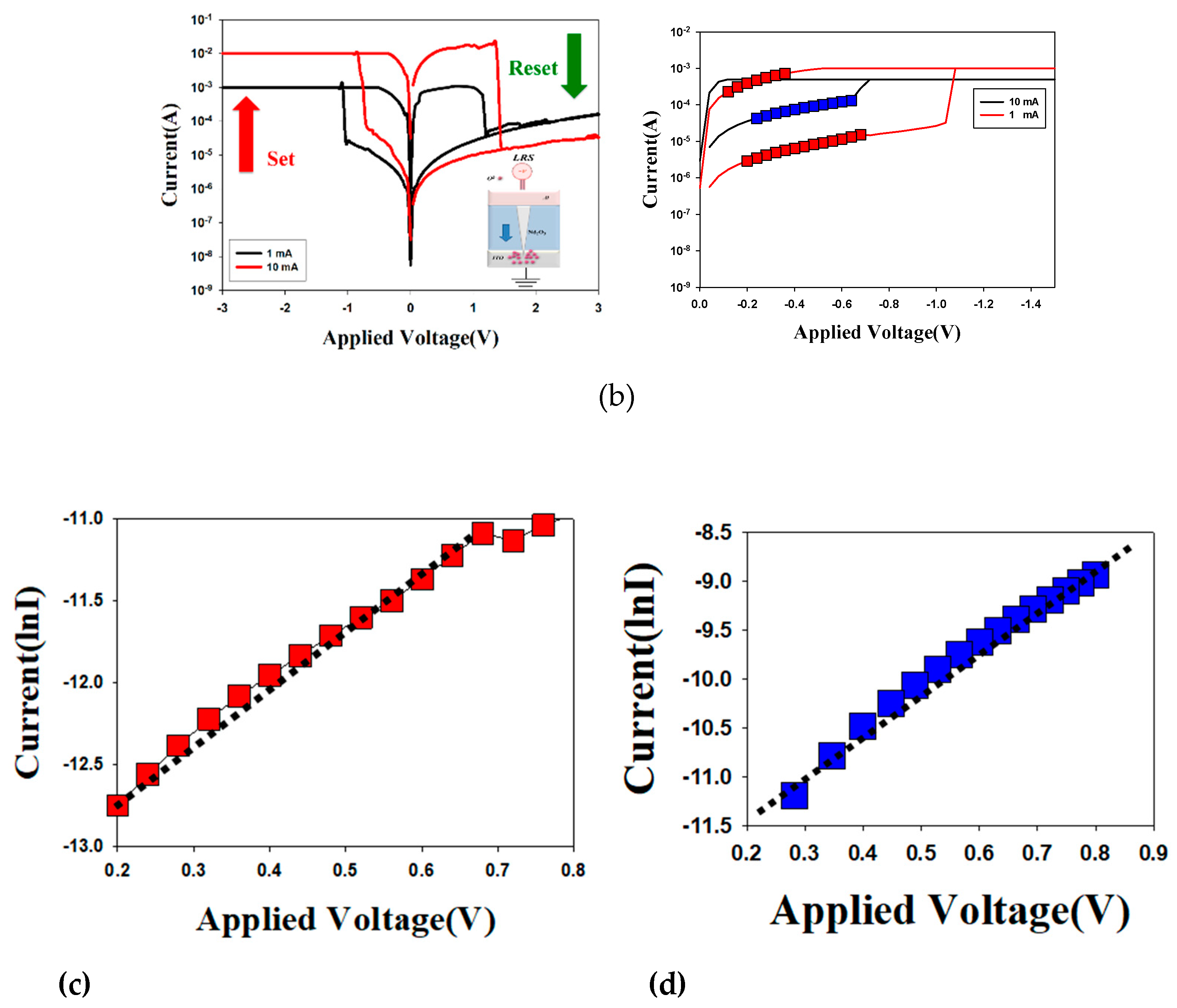
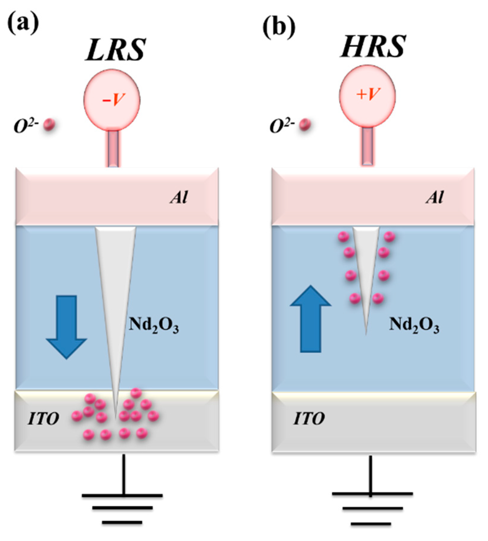
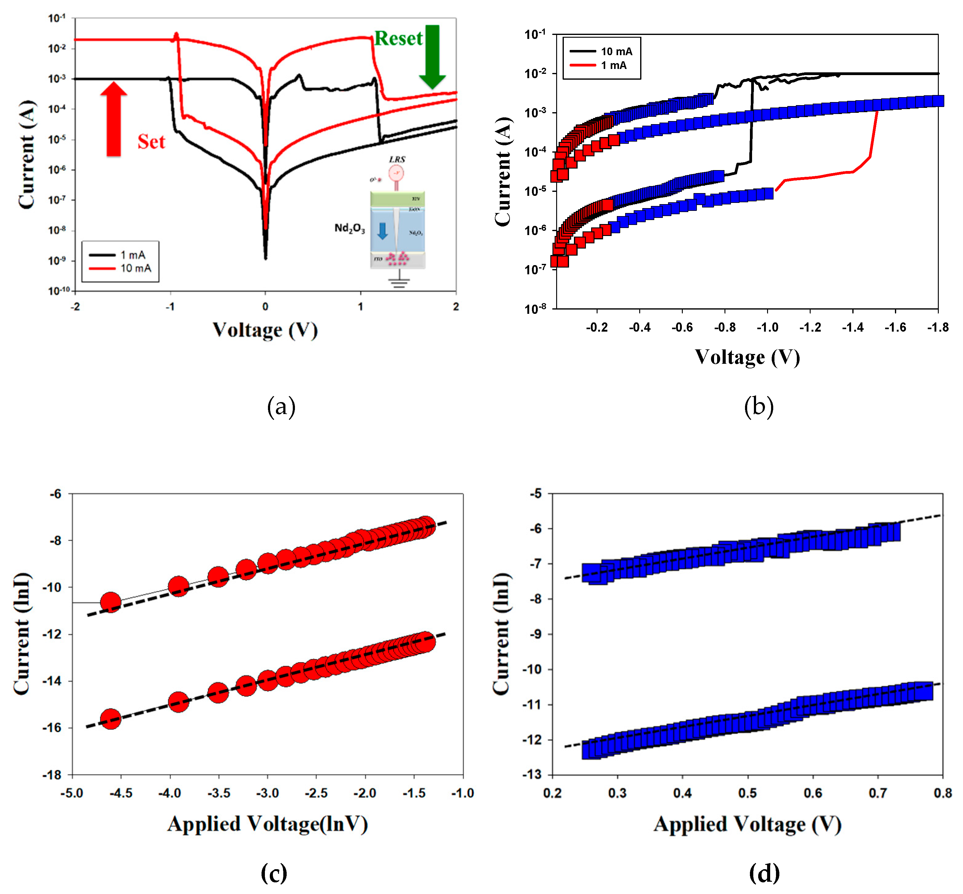
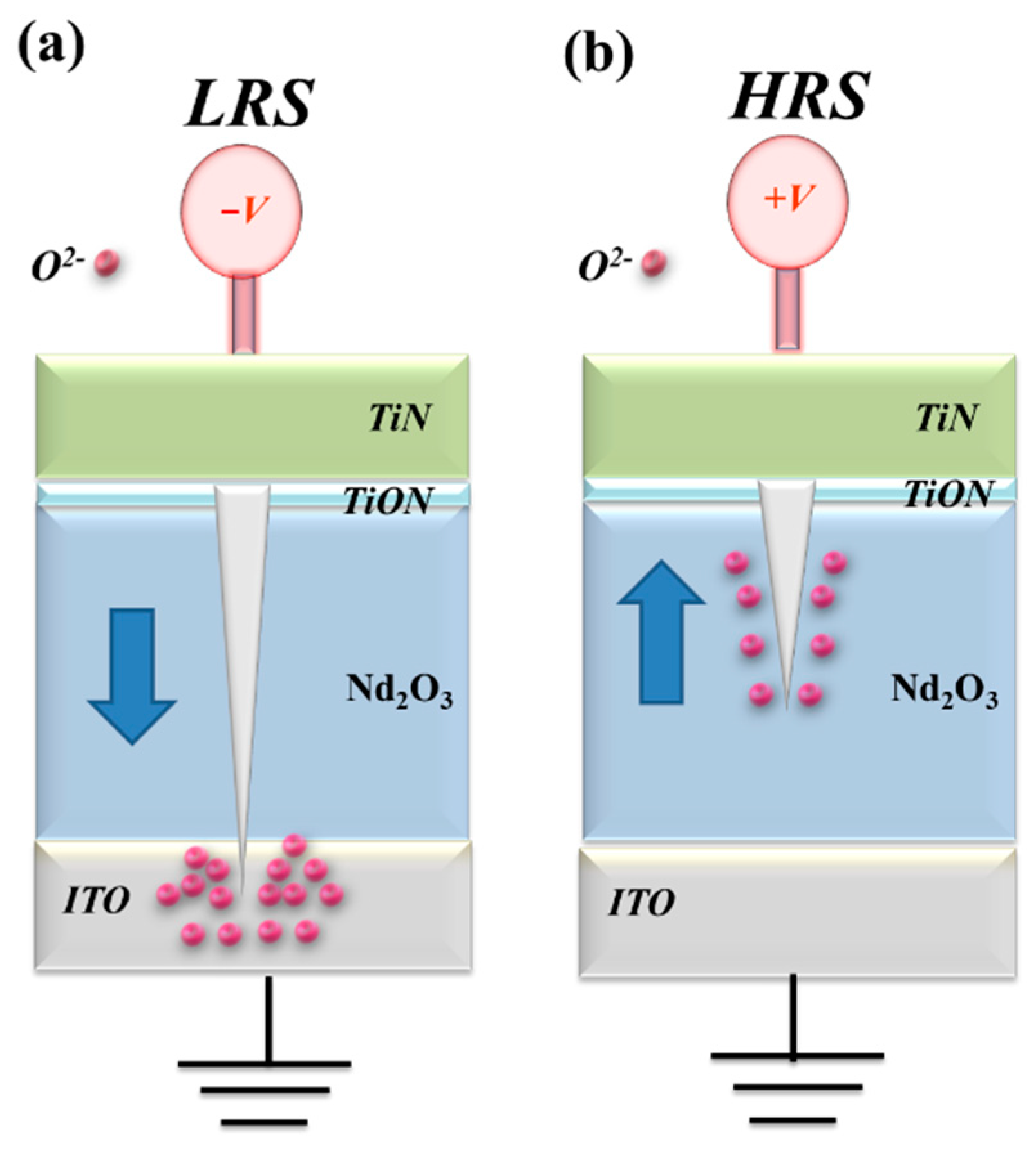
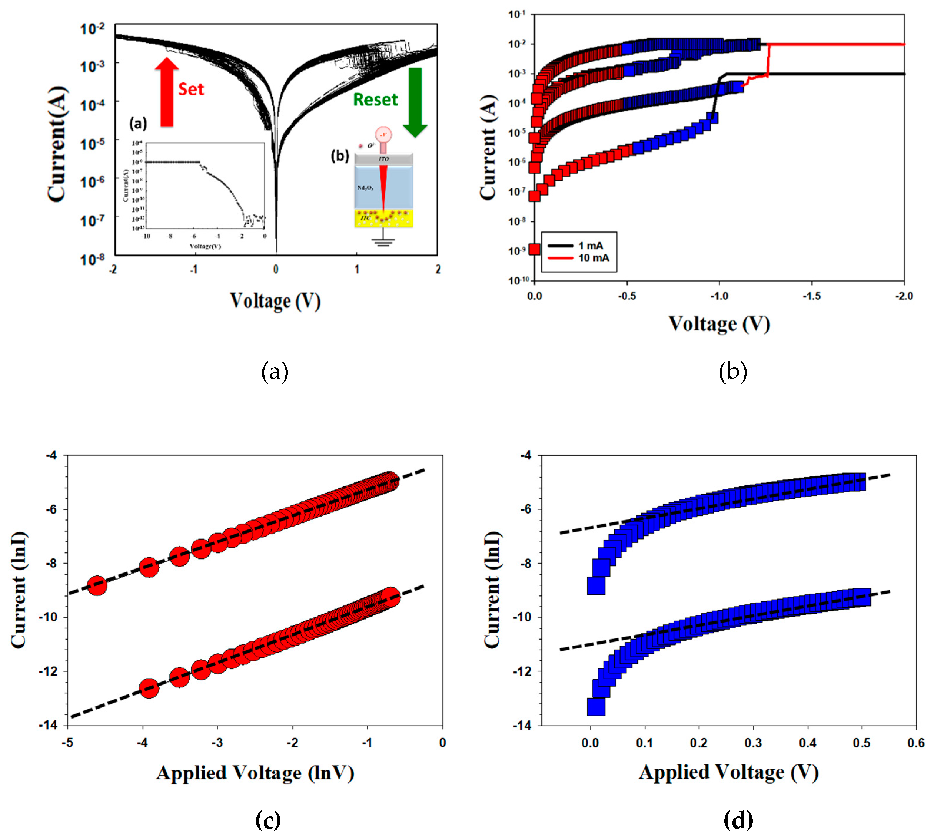
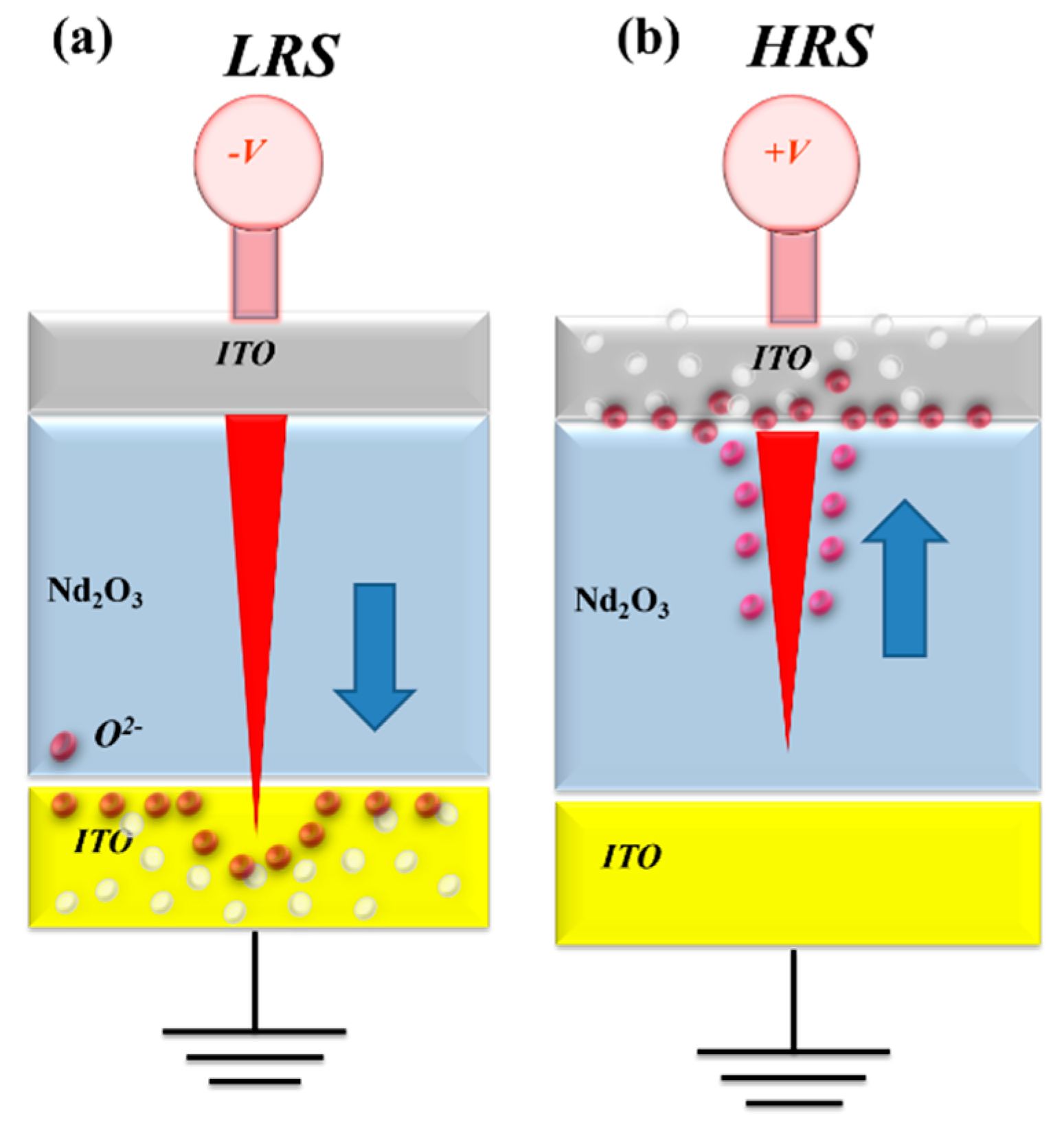
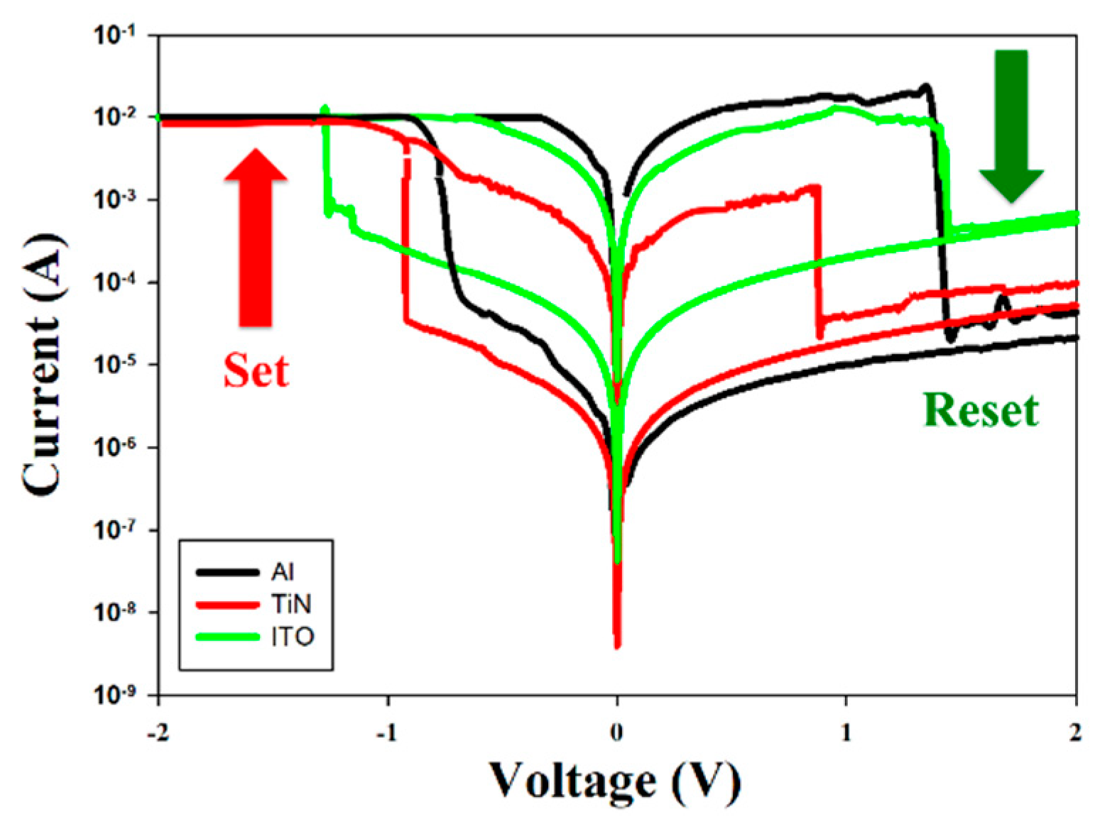
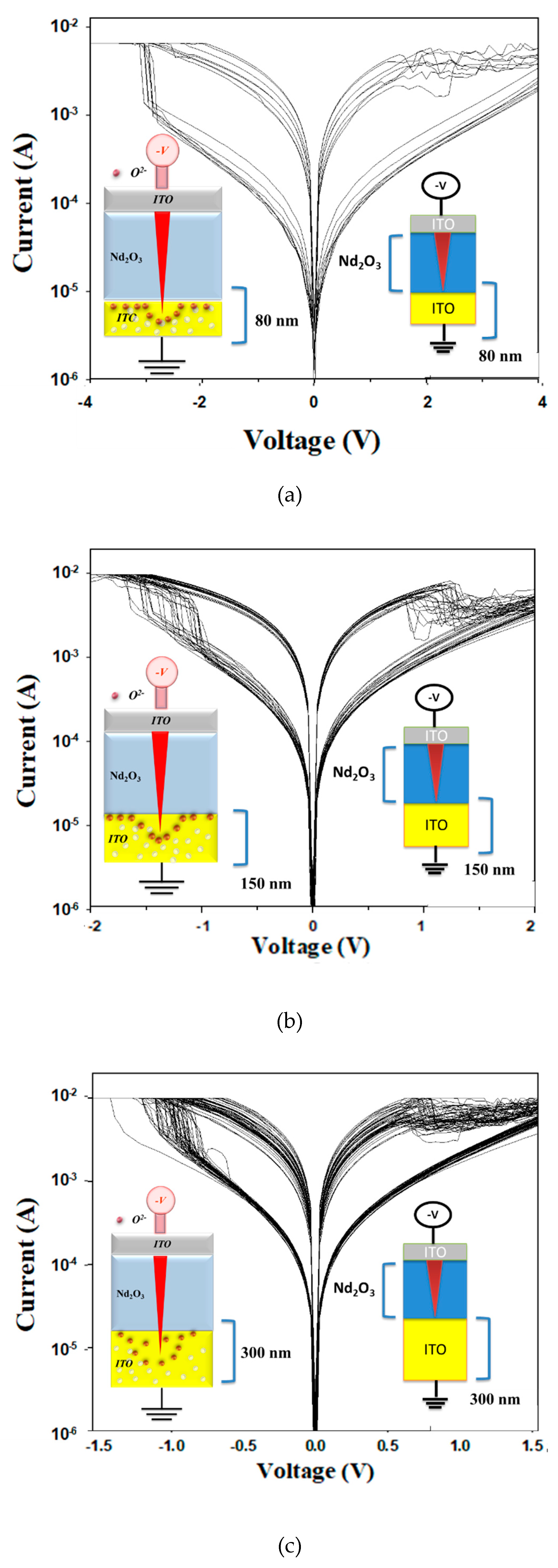
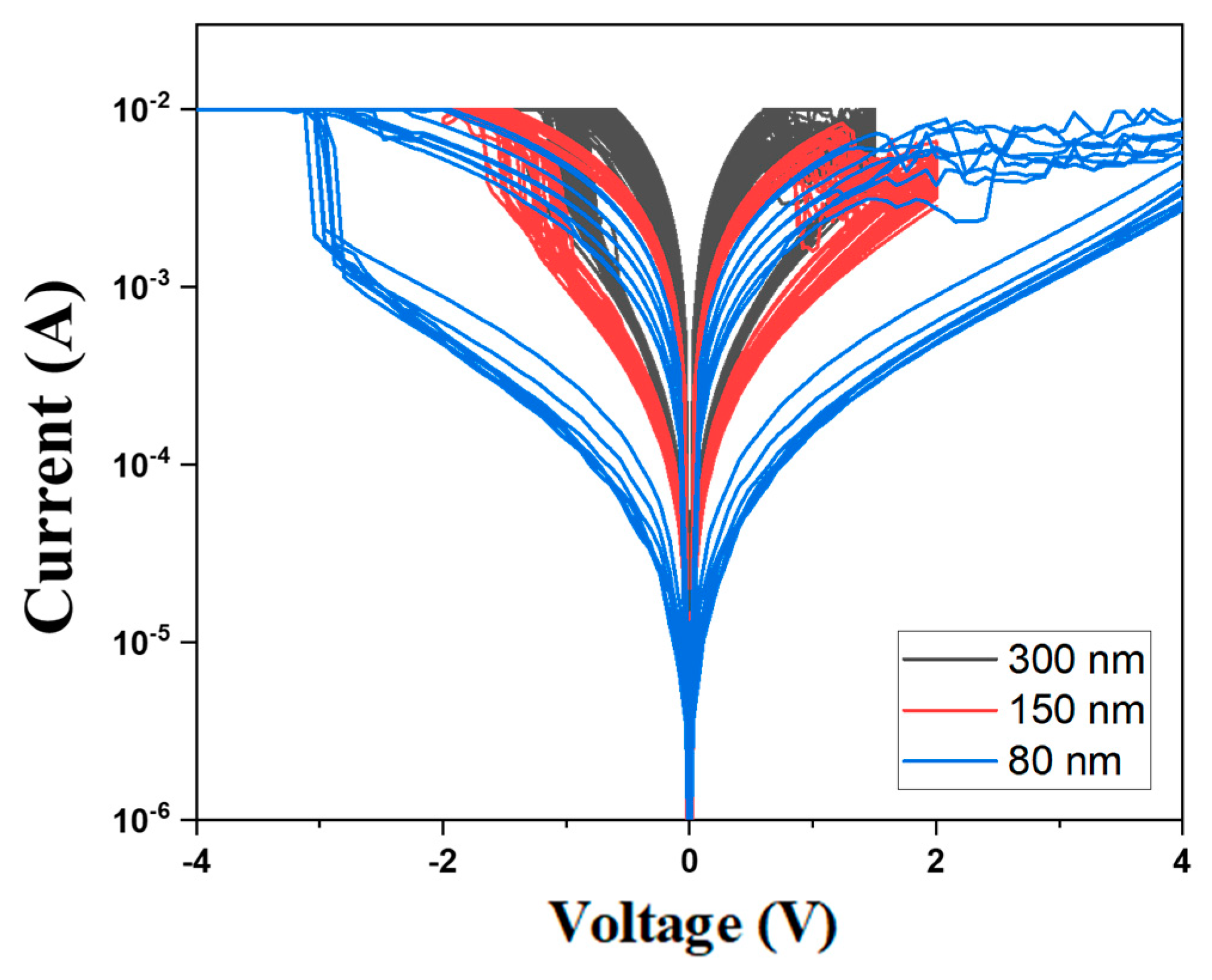
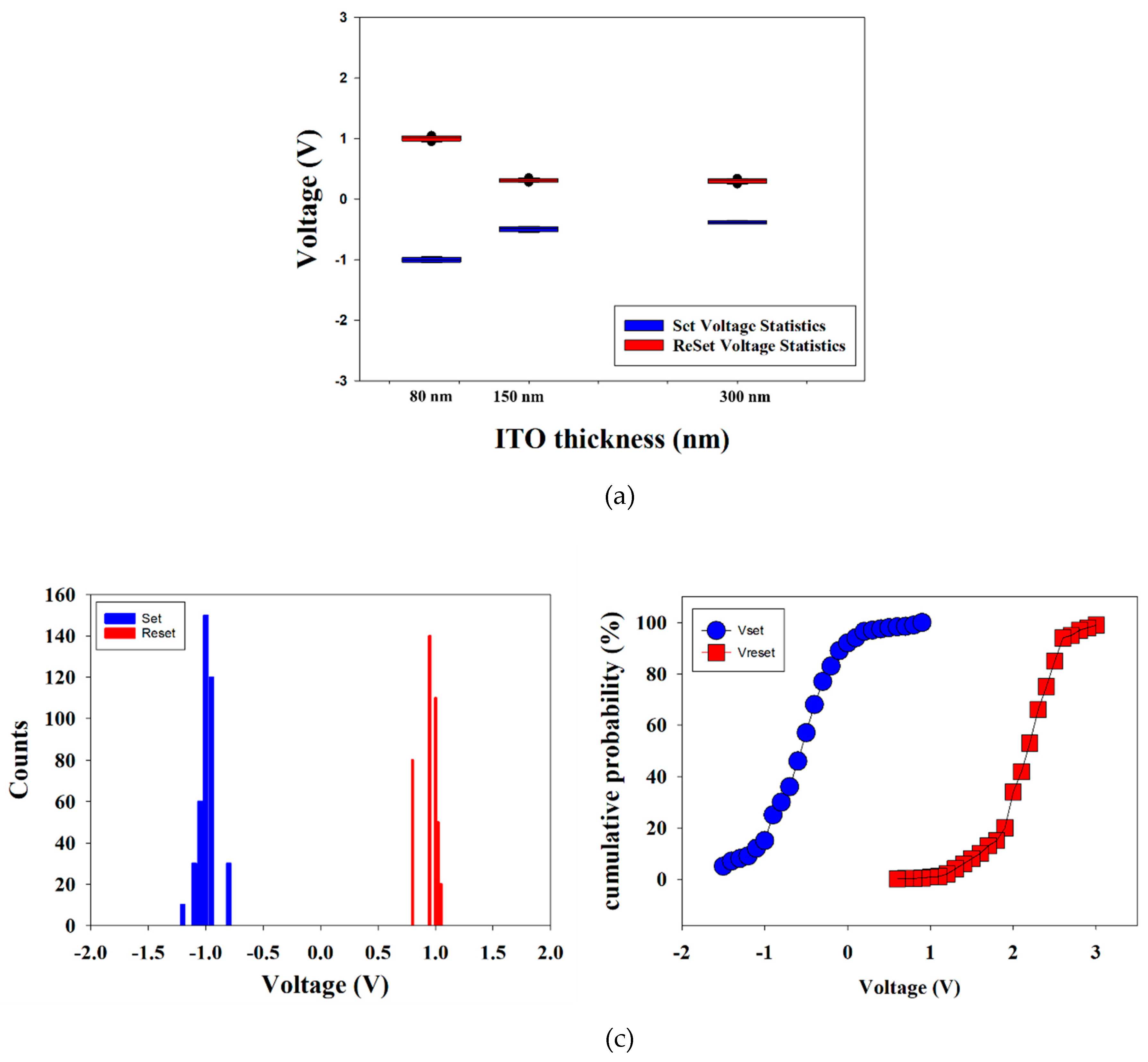
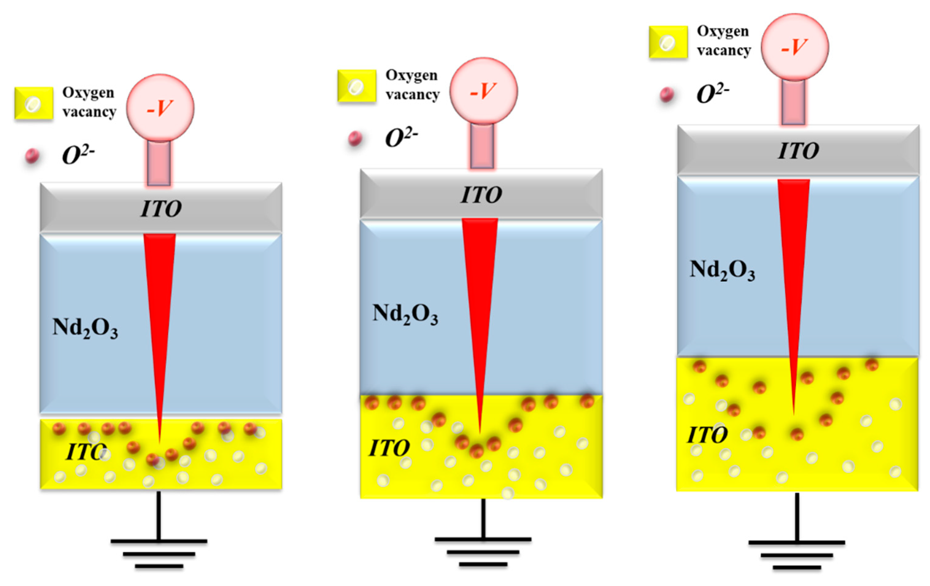
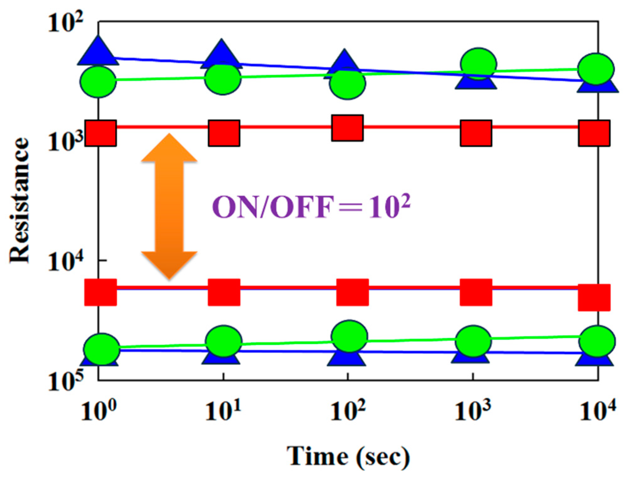
The present study observed and discussed the bipolar resistance switching behavior and electrical conduction transport properties of the neodymium oxide films resistive random access memory (RRAM) devices for the different thickness top electrode materials. Especially in ITO (Indium tin oxide) electrode materials, the conduction mechanism of neodymium oxide films RRAM devices for ITO electrode exhibits ohmic conduction behavior with 1 mA and 10 mA compliance currents in the set state for low operating voltages and low/high resistance values. In addition, at elevated operating voltages, the conduction mechanism displays hopping conduction behavior with 1 mA and 10 mA compliance currents. The observed increase in reset voltage indicates that oxygen ions have diffused into the vicinity of the ITO electrode during the set operation. Three hypothetical physical models are proposed, based on the relationship between different ITO electrode thicknesses and the oxygen concentration distribution effect. In conclusion, the neodymium oxide films RRAM devices exhibited high memory window properties, exemplary bipolar resistance switching characteristics, and non-volatile properties, rendering them suitable for incorporation into next-generation non-volatile memory applications.
Keywords:
1. Introduction
2. Experiment
3. Results and Discussion
4. Conclusions
Author Contributions
Funding
Data Availability Statement
Conflicts of Interest
References
- Li, L., Dai, T.J., Liu, K., Chang, K.C., Zhang, R., Lin, X., Liu, H.J.; Lai, Y.C.; Kuo, T.P. “Achieving Complementary Resistive Switching and Multi-Bit Storage Goals by Modulating the Dual-Ion Reaction through Supercritical Fluid-Assisted Ammonization”, Nanoscale 2021, 13, 14035–14040. [CrossRef]
- Li, L.; Chang, K.-C.; Lin, X.; Lai, Y.-C.; Zhang, R.; Kuo, T.-P. Variable-temperature activation energy extraction to clarify the physical and chemical mechanisms of the resistive switching process. Nanoscale 2020, 12, 15721–15724. [CrossRef]
- Li, L.; Chang, K.-C.; Ye, C.; Lin, X.; Zhang, R.; Xu, Z.; Zhou, Y.; Xiong, W.; Kuo, T.-P. An indirect way to achieve comprehensive performance improvement of resistive memory: when hafnium meets ITO in an electrode. Nanoscale 2019, 12, 3267–3272. [CrossRef]
- Chang, K.-C.; Dai, T.; Li, L.; Lin, X.; Zhang, S.; Lai, Y.-C.; Liu, H.-J.; Syu, Y.-E. Unveiling the influence of surrounding materials and realization of multi-level storage in resistive switching memory. Nanoscale 2020, 12, 22070–22074. [CrossRef]
- Chang, K.C.; Zhang, R.; Chang, T.C.; Tsai, T.M.; Chu, T.J.; Chen, H.L.; Shih, C.C.; Pan, C.H.; Su, Y.T.; Wu, P.J.; “ High Performance, Excellent Reliability Multifunctional Graphene Oxide Doped Memristor Achieved by Self-Protective Compliance Current Structure”, In Proceedings of the IEEE International Electron Devices Meeting (IEDM), San Francisco, CA, USA, 15–17 Dec. 2014; pp. 33–34. [CrossRef]
- Ye, C.; Xu, Z.; Chang, K.-C.; Li, L.; Lin, X.; Zhang, R.; Zhou, Y.; Xiong, W.; Kuo, T.-P. Hafnium nanocrystals observed in a HfTiO compound film bring about excellent performance of flexible selectors in memory integration. Nanoscale 2019, 11, 20792–20796. [CrossRef]
- Lanza, M.; Waser, R.; Ielmini, D.; Yang, J.J.; Goux, L.; Suñe, J.; Kenyon, A.J.; Mehonic, A.; Spiga, S.; Rana, V.; et al. Standards for the Characterization of Endurance in Resistive Switching Devices. ACS Nano 2021, 15, 17214–17231. [CrossRef]
- Sebastian, A.; Le Gallo, M.; Khaddam-Aljameh, R.; Eleftheriou, E. Memory devices and applications for in-memory computing. Nat. Nanotechnol. 2020, 15, 529–544. [CrossRef]
- Sebastian, A.; Le Gallo, M.; Khaddam-Aljameh, R.; Funck, C.; Menzel, S. “Comprehensive Model of Electron Conduction in Oxide-Based Memristive Devices”, ACS Appl. Electron. Mater. 2021, 3, 3674–3692.
- Dalgaty, T.; Castellani, N.; Turck, C.; Harabi, K.-E.; Querlioz, D.; Vianello, E. In situ learning using intrinsic memristor variability via Markov chain Monte Carlo sampling. Nat. Electron. 2021, 4, 151–161. [CrossRef]
- Lanza, M.; Wong, H.-S.P.; Pop, E.; Ielmini, D.; Strukov, D.; Regan, B.C.; Larcher, L.; Villena, M.A.; Yang, J.J.; Goux, L.; et al. Recommended Methods to Study Resistive Switching Devices. Adv. Electron. Mater. 2018, 5, 1800143. [CrossRef]
- Chen, K.-H.; Cheng, C.-M.; Wang, N.-F.; Hung, H.-W.; Li, C.-Y.; Wu, S. First Order Rate Law Analysis for Reset State in Vanadium Oxide Thin Film Resistive Random Access Memory Devices. Nanomaterials 2023, 13, 198. [CrossRef]
- Tsai, T.-M.; Chang, K.-C.; Chang, T.-C.; Zhang, R.; Wang, T.; Pan, C.-H.; Chen, K.-H.; Chen, H.-M.; Chen, M.-C.; Tseng, Y.-T.; et al. Resistive Switching Mechanism of Oxygen-Rich Indium Tin Oxide Resistance Random Access Memory. IEEE Electron Device Lett. 2016, 37, 408–411. [CrossRef]
- Zhang, R.; Young, T.-F.; Chen, M.-C.; Chen, H.-L.; Liang, S.-P.; Syu, Y.-E.; Sze, S.M.; Chang, K.-C.; Chang, T.-C.; Tsai, T.-M.; et al. Characterization of Oxygen Accumulation in Indium-Tin-Oxide for Resistance Random Access Memory. IEEE Electron Device Lett. 2014, 35, 630–632. [CrossRef]
- Yang, C.; Zou, S.; Chen, X.; Gao, J.; Liu, W.; Yang, M.; Xu, J.; Kang, J.; Bu, W.; Zheng, K.; et al. The fabrication of spin transfer torque-based magnetoresistive random access memory cell with ultra-low switching power. Jpn. J. Appl. Phys. 2024, 63, 05SP10. [CrossRef]
- Rong, N.; Liu, X.; Zhang, J.; Xu, P.; Zhang, B.; Song, W.; Song, S.; Song, Z.; Wu, L. High performance antimony-rich RexSb3Te for phase-change random access memory applications. J. Non-Crystalline Solids 2024, 635. [CrossRef]
- Chen, K.-H.; Cheng, C.-M.; Kao, M.-C.; Kao, Y.-H.; Lin, S.-F. Study of the Characteristics of Ba0.6Sr0.4Ti1-xMnxO3-Film Resistance Random Access Memory Devices. Micromachines 2024, 15, 1143. [CrossRef]
- Chen, K.-H.; Kao, M.-C.; Huang, S.-J.; Li, J.-Z. Bipolar Switching Properties of Neodymium Oxide RRAM Devices Using by a Low Temperature Improvement Method. Materials 2017, 10, 1415. [CrossRef]
- H.R. Naderi, H.R. Mortaheb, A. Zolfaghari, “Supercapacitive properties of nanostructured MnO2/exfoliated graphite synthesized by ultrasonic vibration”, J. Electroanal. Chem., 719 (2014), pp. 98-105. [CrossRef]
- Pandolfo, A.; Hollenkamp, A.F. Carbon properties and their role in supercapacitors. J. Power Sources 2006, 157, 11–27. [CrossRef]
- Khadija Tul Kubra, Rehana Sharif, Bebi Patil, Atif Javaid, Shamaila Shahzadi, Ayesha Salman, Sofia Siddique, Ghulam Ali,” Hydrothermal synthesis of neodymium oxide nanoparticles and its nanocomposites with manganese oxide as electrode materials for supercapacitor application”, Journal of Alloys and Compounds, 815, 30, 2020, 152104. [CrossRef]
- Y.E. Syu, T.C. Chang, “Redox Reaction Switching Mechanism in RRAM Device With Pt/CoSiO X /TiN Structure”, Elect. Dev. Lett.32, 545 (2011). [CrossRef]
- Chen, K.-H.; Cheng, C.-M.; Chen, M.-L.; Pan, Y.-Y. Bipolar Switching Properties of the Transparent Indium Tin Oxide Thin Film Resistance Random Access Memories. Nanomaterials 2023, 13, 688. [CrossRef]
- Chen, K.-H.; Cheng, C.-M.; Wang, N.-F.; Kao, M.-C. Activation Energy and Bipolar Switching Properties for the Co-Sputtering of ITOX:SiO2 Thin Films on Resistive Random Access Memory Devices. Nanomaterials 2023, 13, 2179. [CrossRef]
- Chen, K.-H.; Kao, M.-C.; Huang, S.-J.; Li, J.-Z. Bipolar Switching Properties of Neodymium Oxide RRAM Devices Using by a Low Temperature Improvement Method. Materials 2017, 10, 1415. [CrossRef]
- Hsu, C.-C.; Wang, S.-Y.; Lin, Y.-S.; Chen, Y.-T. Self-rectifying and interface-controlled resistive switching characteristics of molybdenum oxide. J. Alloy. Compd. 2018, 779, 609–617. [CrossRef]
- Lee, D.; Seong, D.-J.; Jo, I.; Xiang, F.; Dong, R.; Oh, S.; Hwang, H. Resistance switching of copper doped MoOx films for nonvolatile memory applications. Appl. Phys. Lett. 2007, 90, 122104. [CrossRef]
- Rasool, A.; Amiruddin, R.; Mohamed, I.R.; Kumar, M.S. Fabrication and characterization of resistive random access memory (ReRAM) devices using molybdenum trioxide (MoO3) as switching layer. Superlattices Microstruct. 2020, 147. [CrossRef]
- Yang, C.-S.; Shang, D.-S.; Chai, Y.-S.; Yan, L.-Q.; Shen, B.-G.; Sun, Y. Moisture effects on the electrochemical reaction and resistance switching at Ag/molybdenum oxide interfaces. Phys. Chem. Chem. Phys. 2016, 18, 12466–12475. [CrossRef]
- Xue, Q.; Wang, Y.-C.; Wei, X.-H. Synaptic plasticity of room-temperature fabricated amorphous MoO film based memristor. Appl. Surf. Sci. 2019, 479, 469–474. [CrossRef]
- Fatheema, J.; Shahid, T.; Mohammad, M.A.; Islam, A.; Malik, F.; Akinwande, D.; Rizwan, S. A comprehensive investigation of MoO3based resistive random access memory. RSC Adv. 2020, 10, 19337–19345. [CrossRef]
- Arita, M.; Kaji, H.; Fujii, T.; Takahashi, Y. Resistance switching properties of molybdenum oxide films. Thin Solid Films 2012, 520, 4762–4767. [CrossRef]
- J. Zhao,C. Ma,W. Mi,Di W. Yu Zhang,Liwei Zhou “Optimizing molybdenum oxide based RRAM with vacuum rapid thermal annealing and carbon quantum dots”,Vacuum,225, 2024,113266. [CrossRef]
- Wiśniewski, P.; Mazurak, A.; Jasiński, J.; Beck, R.B. Study of silicon-oxide RRAM devices based on complex impedance spectroscopy. Solid-state Electron. 2023, 208. [CrossRef]
- Qin, S.; Ma, Y.; Wang, Q.; Zhang, J.; Zhang, G.; Yang, L.; Liu, R. Study on ion dynamics of hafnium oxide RRAM by electrode thermal effect. Energy Rep. 2022, 9, 1036–1043. [CrossRef]

| ROW | STRUCTURE | VSET/VRESET (V) | On/Off RATIO | ENDURANCE $(CYCLES) | REF |
|---|---|---|---|---|---|
| 1 | Al/MoOx/Pt | 3/-3 | ∼160 | 500 | [26] |
| 2 | Cu/Cu doped MoOx/Pt | 0.5/-1.5 | ∼23 | 106 | [27] |
| 3 | Ag/MoO3/ITO | 8/-8 | ∼1.28 | 25 | [28] |
| 4 | Ag/MoO3-x/FTO | 1.8/-1.1 | ∼8 | 10 | [29] |
| 5 | Ag/MoOx/ITO | 0.4/-0.067 | >10 | – | [30] |
| 6 | Ni/MoO3/Mo | 3.3/-2.3 | <10 | 17 | [31] |
| 7 | Pt–Ir/MoOx/Pt | 3/-0.7 | ∼10 | 35 | [32] |
| 8 | Ag/MoOx/CQDs/Pt | 0.36/-0.25 | ∼70 | 107 | [33] |
| 9 | Al/SiO2/Si | 1/-2 | ∼10 | 10 | [34] |
| 10 | TiN/HfO2/TiN | 0.4/-0/4 | <10 | 10 | [35] |
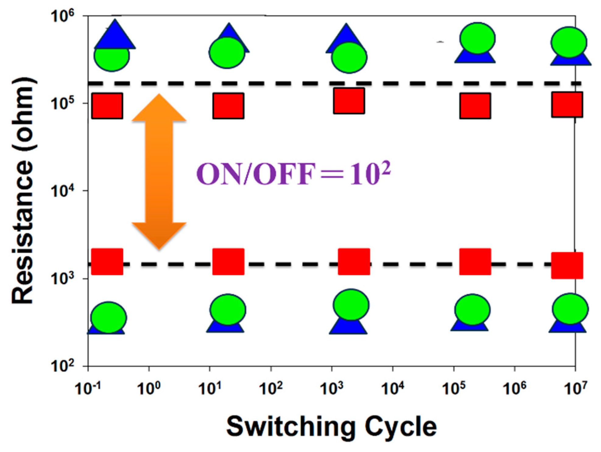
| 11 | ITO/Nd2O3/ITO | 1/-1 | >102 | 107 | This work |
Disclaimer/Publisher’s Note: The statements, opinions and data contained in all publications are solely those of the individual author(s) and contributor(s) and not of MDPI and/or the editor(s). MDPI and/or the editor(s) disclaim responsibility for any injury to people or property resulting from any ideas, methods, instructions or products referred to in the content. |
© 2024 by the authors. Licensee MDPI, Basel, Switzerland. This article is an open access article distributed under the terms and conditions of the Creative Commons Attribution (CC BY) license (http://creativecommons.org/licenses/by/4.0/).


