
Submitted:
22 November 2024
Posted:
26 November 2024
You are already at the latest version
Abstract
The possibility of inducing structural crosslinking and densification of plasma-deposited SiOx networks, by controlling low energy reaction mechanisms was investigated. For this, films were deposited for 300 s from HMDSO (2%), O2 (86%) and Ar (12%) mixtures at a working pressure of 15.7 Pa. A radiofrequency signal was used to excite the plasma in a configuration to not deliberately induce ion bombardment of the growing layers. Plasma excitation power was varied (100 to 300 W) to promote changes in the deposition mechanisms, which were investigated from deposition rate and layer thickness, chemical structure, elemental composition, topography, roughness, hardness, elastic modulus, corrosion potential, corrosion current density and porosity of the films. Under the experimental conditions studied, inorganic SiOx thin films (x=1.8-1.9) with low carbon content were deposited. The increase in the applied power during the deposition process reduced the number of silanol groups in the coatings, which became more compact, and consequently, harder and more corrosion resistant.
Keywords:
SiOx
; HMDSO
; plasma deposition
; crosslinking
; corrosion resistance
; mechanical properties
1. Introduction
Silicon oxide films have found practical applications as protective anti-scratch coatings for ophthalmic lenses [1,2], barrier-type films for food and pharmaceutical packaging [3], coatings for biocompatible materials [4], dielectric layers in microelectronics [5,6] and coatings for metal protection. This wide variety of applications is ascribed to the film’s structural flexibility, enabling the combination of a series of required properties in different applications. Another convenient aspect is the variety of practical approaches available for their preparation, including electrodeposition [7], sol gel deposition [8] , dip coating [9], atomic layer deposition [10] and plasma enhanced chemical vapor deposition [11], PECVD. Of these, the PECVD of organosilicon compounds emerges as a versatile possibility owing to its simplicity, low cost, low consumption of reagents and electrical energy, and the generation of little waste product. These attractive characteristics stimulated the investigations by PECVD of organosilanes [12,13,14,15,16] for production of SiOx films.
Among the organosilicon compounds, tetraethoxysilane (TEOS) and hexamethyldisiloxane (HMDSO) are the most common precursors for plasma deposition of SiOx films, with the deposition mechanisms having already been deeply investigated [17,18,19,20,21,22,23]. These compounds behave similarly, but HMDSO is more easily fed to the plasma because of its greater volatility (boiling point: about 100°C for HMDSO and about 170°C for TEOS).
In atmospheres containing hexamethyldisiloxane, HMDSO, ([CH3]3SiOSi[CH3]3) [2,3,4,5,6,7], the PECVD process may also provide organosilicon, silicon oxicarbides or a combination of these by varying the deposition conditions [1,2,3,4,5,6,18,19,20,24]. The production of inorganic SiOx groups in plasmas fed HMDSO and oxygen, increases with the addition of argon to the gas mixture [25], with an increase in the plasma excitation power [26] and with pressure [27]. Another possibility is the addition of an oxidant, frequently molecular oxygen, to switch from an organosilicon to an inorganic SiOx coating, by decreasing the organosilicon-to-oxygen ratio in the plasma feed [17,18,28,29]. Nitrogen-containing precursors mixed with oxygen can also be utilized for SiOx deposition [25], leading to silicon nitride-like thin films [26,27]. Besides the feed composition, other parameters also play important roles in determining the final film composition, structure, hardness and porosity: power density, excitation frequency, surface temperature and ion bombardment [19,24,30].
There is consensus in the literature that films with low organic proportions are more efficient for corrosion protection [1,3,20] than organosilicon because of their greater density and chemical inertness. Factors such as silica adhesion to the substrates (metal or polymer), mechanical stress, and especially the defects generated in the deposition process or by substrate finishing however, affect the efficiency and physical stability of the layer and, therefore, its practical application.
Petit-Etienne et al. [27] determined the porosity of silica films deposited from HMDSO plasma and found that the concentration of these defects decrease with greater ion-bombardment intensity. Therefore, although the deposition occurs at the atomic and molecular scale, defects are incorporated and their minimization is of great relevance to the barrier properties of the films.
In the work of Milella et al. [31] an increase in the SiOx film density was shown to be caused by post-deposition ion bombardment in an argon and oxygen plasma [31]. The densification and the topographical smoothening were dependent on the treatment time and voltage applied to induce ion bombardment. In another work by the same authors [2] it was shown that the bombardment of the material surface by low energy ions can lead to the breaking of chemical bonds, diffusion and heating; factors that contribute to the film densification and to a reduction in the structural disorder. Excessive bombardment energies, however, may damage the structure and cause the internal tension of the layer to grow. These results are confirmed by the work of Lefe`vre et al. [32] using molecular dynamic simulations, which show that ionic bombardment during SiOx film growth promotes structural changes, which affect density and internal stress of the films. The films deposited in the absence of ion bombardment presented high tensile stress and, consequently, reduced adhesion to the substrates and resistance to cracking. The low deposition temperature is indicated as the factor responsible for this result.
Densification of plasma-deposited organosilicone films was proposed by Blanchard et al. [33] via control of the plasma excitation power and the self-bias of the driven sample holder. In this work, the role of the excitation power on the plasma homogeneous (gas phase energetics) and heterogeneous (surface ion bombardment) reactions is discussed. Densification is proposed to be not entirely related to ion bombardment during film deposition, but also to the plasma activation state, characterized in terms of the energy delivered per molecule of the plasma phase.
Therefore, considering the importance of densification for protective layers and that the studies in the literature report the densification of silica-based material in association with ion bombardment or heating during or after the deposition process, the proposal of the present work is to investigate the possibility of increasing the density of silica-based films by tailoring homogenous and heterogeneous low energy reactions. The power of the excitation signal was selected as the key experimental variable since it directly influences the energy of the plasma species. Although several reports have already been published on the effect of the plasma excitation parameters on the properties of silicon-based films, the role of the plasma-phase reactions and plasma-surface energetic interactions on the structure densification are not fully understood [33,34].
2. Materials and Methods
Films were deposited in a parallel-plate reactor consisted of a stainless-steel cylindrical chamber, pumped by a turbomolecular-rotary pumping system. The injection of compounds into the reactor was regulated by mass flow controllers and vapor source controller (MKS Instruments, Inc.). The internal pressure was monitored by a baratron gauge and controlled by an automatic throttle valve. The lower electrode, at floating potential, was used as the sample holder.
Ultrasonically cleaned substrates were accommodated in the sample holder and the system pressure reduced to 1.7 Pa. Film deposition was performed for 300 s in an atmosphere composed of HMDSO (0.21 Pa, 4 sccm), O2 (8.11 Pa, 120 sccm) and Ar (1.15 Pa, 45 sccm). The initial pressure of the gases (9.5 Pa) was then adjusted to 15.7 Pa by reducing the pumping velocity but maintaining the proportions of the gases. The plasma was generated by applying a radiofrequency signal (13.56 MHz) to the upper electrode, while the reactor walls were grounded. In all the experiments, deposition time was 300 s. The effects of the plasma excitation power, which was varied from 100 to 300 W, on the films were investigated.
Film thickness (h) was determined from the height of a step produced by film deposition while masking part of Si wafer with a glass plate. The step height was measured in, at least, seven different regions with the aid of an Alpha-Step 500 KLA Tencor profilometer. Deposition rate (R) was derived from the ratio of the thickness and the deposition time.
The chemical structure of the films deposited onto polished silicon plates was analyzed by infrared reflectance-absorbance spectroscopy (IRRAS) in a Bruker Equinox 55 spectrometer. For each spectrum, 32 scans were performed in the 375 - 4000 cm-1 range and with resolution of 4 cm-1. Elemental composition and chemical bonding state of the film surfaces were derived from X-ray photoelectron spectroscopy (XPS). Data were acquired in a PHI 5300 ESCA spectrometer using MgKα radiation and with 0.05 eV of energy resolution. High resolution spectra (Si 2p) were registered at an electron take-off angle of 45° and after 20 s of surface cleaning using Ar+ ion sputtering (1 keV). High resolution spectra were calibrated in energy by the reference Si 2p peak at 103.4 eV (SiO2) and fitted with Gaussian peaks after subtraction of the Shirley-type background. XPS analyses were conducted on samples deposited onto silicon plates.
Mechanical and tribological properties of the films were examined, respectively, by nanoindentation and scratching tests in a Hysitron TI 750 UbiTM Nanoindentation system with the performechTM control scanning unit. Indentations were conducted at 15 different positions on each sample using a diamond Berkovich tip and a partial unload function of 5000 μN. Hardness and elastic modulus were calculated from the load displacement curves according to the Oliver Pharr method [35]. The tip area function was calibrated from the results of indentations on a fused quartz before the experimental test.
Topographic images of the surfaces were taken before and after indentations by scanning the same Berkovick tip, under a 2 µN load, over a 5 µm X 5 µm area. For the scratching experiments, a ramp function of 200 µN of maximum load was applied to the tip while displacing it by 10 µm. To evaluate the surface damage, new AFM topographic profiles (10 µm X 10 µm) were taken after the scratching procedure. All the above mentioned mechanical and tribological tests were performed in samples prepared in silicon substrates. However, for inspecting the behavior of the films under higher loads and in different substrates, scratching experiments were repeated in samples prepared on carbon steel substrates. For that, a ramp function of 30 mN of maximum load was applied to the tip while displacing it by 80 µm with 2 μm/s of speed. To evaluate the surface damage, optical images were taken using the microscope coupled to the nanoindenter system.
The corrosion resistance of the as-received and film containing carbon steel (NBR 5915) plates, in NaCl solution (3.5%), was derived from potentiodynamic polarization measurements. The analysis was carried out in a conventional electrochemical cell with three electrodes. Carbon steel samples were used as the working electrodes while the counter and reference electrodes were platinum/rhodium and silver plates, respectively. Current density was recorded while changing the potential from the cathodic region (-0.25 V) to the anodic one (0.25 V), at a rate of 0.17 mV/s. The linear regions of the anodic and cathodic portions were extrapolated to derive the corrosion potential, Ecorr, and the current density, Icorr, as proposed by Zhang et al. [36].
3. Results
3.1. Thickness and Deposition Rate
The thickness, h, and deposition rate, R, of the films are shown in Figure 1 (a) as a function of the plasma excitation power, P. There is a slight variation in h as P is increased from 100 to 200 W, but a steep drop (~50%) appears at the highest P value (300 W). As deposition time was kept constant (300 s) in all the experiments, the deposition rate follows exactly the same trend as h, decreasing from 95 to 59 nm/min (38%) as P is increased from 100 to 300 W.
In the work of Wavhal et al. [37] a reduction in the deposition rate was also observed when high O2/HMDSO ratios were used. The authors ascribed this trend to severe fragmentation and oxidation of the organosilicon molecule by the plasma. On the other hand, Vendemiatti et al. [38] reported an increase in deposition rate as the proportion of oxygen in O2/Ar/HMDSO mixtures increased from 0 to 30% (while Ar was decreased from 30 to 0%). But at the high HMDSO proportion (70%) used in that work, the oxygen content was not sufficient to fully fragment oxide groups but only to enhance the concentration of polymerizable (CH3)3-Si-O-, (CH3)3-Si-O-Si-O-(CH3)2, Si-(CH3)3 and CH3 species in the plasma phase, thus accelerating deposition rate.
Thus, the falls observed in the curves of Figure 1 (a) are ascribed to the intense dissociation of O2 and HMDSO molecules, caused by the increase in applied power. The activity of the plasma [39], defined as the product of the average electron energy and its density, increases with P turning the activation process more effective. Besides increasing the average energy and density of the activated species, increased power also increases its reactivity since a greater variety of fragments are generated. It was demonstrated, for instance, that the concentration of oxygen radicals increases with P in pure O2 plasmas, especially in high-pressures processes, such as those employed in the present work (16 Pa) [24]. The overall availability of film-forming species is reduced by oxidation while the removal of newly deposited groups by heterogeneous reactions is increased, both effects contributing to the diminishing trends shown by the curves of Figure 2.
3.2. Chemical Structure an Elemental Composition
The infrared spectra of the films investigated here are shown in Figure 1 (b). Table 1, summarizes the wavenumber of the main absorption bands found in the spectra and their respective assignments. The most prominent band, lying at 1062 cm-1, is associated to the Si-O stretching vibration of SiOx groups. When this band is centered between 1075 and 1080 cm-1, a SiO2 stoichiometric structure is expected [40]. When shifted to lower wavenumbers, however, as in the spectra of Figure 1 (b), a SiOx non-stoichiometric network is indicated. The shift of the vibrational frequency downwards derives from the replacement of Si-O by Si-Si bonds thus revealing further chain connections and a denser silicon-based material [40]. The full width at half maximum (FWHM) of this contribution is also dependent of the structural organization. In the stoichiometric SiO2 structure, the FWHM of the band is around 80 cm-1 while wider peaks, as the observed here (224 cm-1), are found in SiOx crosslinked networks [40]. The bands in 815 and in 445 cm-1, detected in all the spectra, are associated, respectively, with rocking and bending modes of Si-O.
The spectrum of the film deposited at the lowest power, 100 W, presents two other bands at 935 and 3500 cm-1 which are attributed to OH vibrations in Si-OH. The abstraction of methyl groups from the methylsilyl functional, in the solid or plasma phase, traps free radicals in the film structure. The incomplete consumption of dangling bonds by chain crosslinking keeps residual radicals active in the film. Permeation of oxygen and water vapor through the structure, as the sample is exposed to air, eventually saturates the bonds by incorporation of hydroxyl groups. The incorporation may also occur by heterogeneous low energy reactions taking place during film deposition. Besides preventing the establishment of Si-Si connections, SiOH groups act as reactive points where degradation reactions may initiate in contact with water or its vapor [41]. Therefore, the presence of the SiOH functionals suggests a more reactive and less crosslinked structure, which are negative points in relation to mechanical and chemical resistance as well as structural permeability. Finally, the presence of free-OH molecules in the structure is revealed by the increase in the low intensity band around 3650-3690 cm-1 [42].
It should be taken into account here that a diversity of fragments can be generated from the HMDSO molecule, depending on the plasma activity [39]. When deposition is conducted in the low fragmentation regime, that is, using low power or high flow ratios, the oligomerization of high molecular weight fragments gives rise to species much larger than the original precursor molecule [43]. The deposition of such huge, organic-rich molecules generates an organosilicon structure very similar to that of conventional polydimethylsiloxane (PDMS) or silicone. In this case, the presence of methylsilyl (Si(CH3)), dimethylsilyl (Si(CH3)2) and trimethylsilyl (Si(CH3)3) groups connected to the Si-O-Si backbone [44] is readily detected in the infrared spectrum of the material by an absorption band lying at 1260 cm-1. Furthermore, depending on the degree of activation, a crosslinked PDMS-like structure is generated, such as the one proposed by Blanchard et al. [33] and Rangel et al. [45].
On the other hand, when high excitation powers [46] or elevated proportions of oxygen [44,47] or both are used, there is severe fragmentation of the organosilicon precursor. In the oxygen rich atmosphere, the fragments can be further dissociated and oxidized, generating CO, H2O and OH volatile groups [44]. As these low molecular weight species have low sticking probabilities [46,48] they do not effectively contribute to film formation, being eventually removed from the deposition chamber. Heterogeneous plasma-surface reactions also contribute to abstraction of organics from the deposited material [44], generating extra pendant bonds. When such mechanisms predominate, there is the formation of a SiO2-rich structure with organics appearing just as contaminants. This regime, proposed as an explanation for the results of Figure 1 (b), is based on a deposition mechanism involving low energy deposition by ion bombardment, which is consistent with a sample holder at floating potential.
The film elemental composition and chemical bonding state were analyzed by XPS. The wide range XPS spectra of the films (not shown) revealed the presence of C, O and Si, being their atomic proportions presented in Table 2, together with the O/Si atomic ratio. Only traces of C (≤ 1%) were detected while O (65%) and Si (34%) represent the main elements of the film surface. Furthermore, no significant changes in these concentrations were detected as the applied power was varied.
In a study by Wavhal et al. [44] changes in the concentration of C and O were observed as the excitation power was changed from 25 to 125 W, however a stabilization was detected for the highest excitation powers, in good agreement with the results presented here: the low carbon content and the O/Si ratio around 1.8 - 1.9 characterize a SiO2-like structure in which an ideal ratio of 2.0 is expected. Therefore, the excess of Si with respect to O corroborates the idea of replacement of Si-O by Si-Si bonds and the structural crosslinking enhancement.
The high-resolution Si 2p spectra obtained from the films studied here are presented in Figure 2. The adjustment of the peaks was conducted considering silicon surrounded by four Si(-O4) (103.4 eV), two Si(-O2) (102.0 eV) and one (101.5 eV) oxygen atoms. These environments for Si are consistent with those used in previous reports within 0.1 eV of tolerance [30,33,44,49]. The proportion of each contribution to the total area of the peak was determined and is presented in Table 3. As can be noticed, the coating is predominantly composed of tetrahedral silicon oxide with the suboxide network appearing at low proportions (< 10%).
The rise in the SiO4 component, which is schematically represented in Figure 3 (a), reflects the high fragmentation imposed to the organosilicon molecule [44]. In these three-dimensionally connected networks, C and hydroxyl moieties are linked to suboxide groups, as depicted in the illustration of Figure 3 (b). The high proportion of SiO4 in the sample prepared at 300 W thus reveals a high-quality oxide structure, obtained without biasing the substrate holder, as normally reported in literature [24,27,50] confirming the hypothesis that ion bombardment is not the only mechanism responsible for that.
The results of this section reveal the formation of a non-stoichiometric three-dimensionally connected SiOx structure (100 W), with the degree of crosslinking rising with increasing deposition power up to 200 W and its eventual evolution into an almost complete tetrahedral network (300 W). Organic contamination was lower as compared to that found in other works [44,49]. Variation of the excitation power, in the range used here, does not change the nature of the film but its spatial organization, inducing crosslinking and preventing organic and SiOH incorporation. The schematic representation of such a structure is presented in Figure 3 (b).
3.3. Surface Topography and Roughness
As the surface finish significantly impacts the final properties of the system, the surface microstructure of the films was also examined. Figure 4 shows 2D and 3D topographic images of the bare silicon substrate and of the silicon-containing SiOx films. The polished silicon has a smooth and flat surface, as observed from the reduced value of the scale of its profile. In general, the surface is uniformly coated by the film with no evidence of cracks, detachment or uncoated areas but with a clear change in the surface morphology after plasma exposure, suggesting the presence of the film.
For the film grown at the lowest applied power (100 W), the surface presents an apparently uniform matrix with white spots sparsely spread upon it. Deposition seems to occur uniformly on the substrate surface with no preferential points for film growth. A similar topography was reported by Zanini et al. [6], when a SiOx coating was prepared from an HMDSO/O2 mixture at moderate plasma pressures.
As P is enhanced (100 - 200 W), the concentration and size of the regular rounded structures increases. The regular matrix is replaced by posts with heights of several nanometers, giving rise to a fakir-like surface, typically found in glassy SiO2 films [51].
Eventually, a topographical smoothing is detected (300 W) with a sudden reduction in the diameter and height of the spikes. As the topographic profile of this sample resembled that of the silicon wafer, new inspections were conducted to verify whether the film was still adhered. The film was readily detected by the unaided eye and infrared spectroscopy inspections, revealing the creation of a fine-grained packed structure.
The spherical particulates on the surface of SiOx films were also reported in previous works [52,53]. The concentration and size of nano-spherical agglomerates in silicon oxide coatings was observed to strongly depend on the proportion of O2 admitted to the plasma environment in the work of Huan et al. [54]. According to the same study, structures composed of larger aggregates of particles give rise to a greater number of pores, which allow gas and moisture permeation, yielding coatings with poor barrier properties.
To understand these results, it should be taken into account that the reduction in the deposition rate, demonstrated in the graph of Figure 1 (a), reveals a modification in the deposition kinetics. The first elevation of power from 100 to 200 W, without changing deposition rate and thickness, favors the plasma polymerization process and explains the enlargement of globular structures in the film. The elimination of organics from the precursor molecules with further increasing P to 300 W, reduces the size and the availability of film-forming species. A reduction in the rate that they arrive at the surface gives extra time for re-arrangements to occur. The incorporation of defects (voids) thus decreases with both the reduction in the size of the depositing fragments and their arrival rate. Therefore, the structural evolution observed here can be attributed to the heightened fragmentation process induced by low-energy reactions, which impact both the concentration and size of the agglomerates in two distinct ways.
The root mean square (RMS) roughness of the samples, derived from the total image area (5 μm X 5 μm), is shown in Figure 5 (a) as a function of P. Roughness values found for the silicon substrates, represented by the dotted line in the graph, ranged from 0.20 to 0.23 nm. These values are consistent with those found in the literature ranging between 0.01 and 0.57 nm [55,56]. The system roughness increases after film deposition, independently of the condition which was employed, with a steady rise appearing as the power is increased from 100 to 200 W. This result is ascribed to the enhancement in the pillar heights. Since film thickness is not significantly changed with this power modification, extra energy provided by the greater power process is used to change the deposition mechanisms, as discussed before. Consistently with the topographic profiles, roughness falls with increasing deposition power beyond 200 W.
Despite being more compact and inert than its organosilicon (SiOxCyHz) counterparts, silica films present defects generated during the deposition process or by the substrate mold effect. Together with these, the internal stress, incorporated in the coating during its deposition, accounts for defect creation. In the work of Petit-Etienne et al. [27], for instance, a reduction in the porosity of silica films was observed when ion bombardment was induced during deposition. Milella et al. [31] demonstrated densification and smoothing of SiOx films deposited by sputtering when post-deposition ion bombardment treatments were conducted, affecting the optical and the electrical properties of the system. In the present work, the changes in the surface topography are attributed mainly to alterations in the plasma kinetic with P since ion bombardment is not that effective when the substrate is at floating potential.
Therefore, even though the power of the plasma excitation signal barely affects chemical composition, it strongly influences the surface topography. With increasing P there was a transition of a rather uniform matrix to a fine-grained smooth SiOx structure.
3.4. Mechanical and Tribological Properties
Figure 5 (b) shows the representative nanoindentation load-displacement curves for the SiOx coatings deposited on silicon which were obtained using a partial unload function (5000 µN). In all cases, the loading and unloading segments are smooth, regular and free of discontinuities, indicating a film adhered to the substrate which did not crack under stress [57]. The maximum penetration depth is observed to decrease with increasing deposition power, indicating a greater tip penetration resistance. Besides, it is noticed that the area under the curve for the film prepared with the lowest power (100 W) differs significantly from the others, indicating a higher plastic deformation.
Figure 6a-d show 2D topographic profiles of the surfaces taken after the nanoindentation procedure. The correspondent result for the bare Si substrate is also included. All indented areas reveal plastic deformation without any cracks around the corners, region where the highest stress is concentrated. The absence of cracks indicates a material with fracture toughness and reliable results for elastic modulus and hardness [24,58].
From the topographic profiles of Figure 6, the lateral distance of the impress, D, was measured along the indent profile, as defined in the work of Tekaya et al. [59]. Results are presented in Figure 6 (e) as a function of P. It is observed a decrease in D with increasing P corroborating the idea of an elevation in the resistance to plastic deformation [59].
The hardness of the samples, determined at depths which represent 15% of the total layer thickness [60,61,62], is depicted in Figure 7 (a) as a function of the plasma excitation power. The film deposited using the lowest P (100 W) presents hardness values close to those reported for SiOx systems [57,63]. Hardness increases threefold (4.5 to 13.3 GPa) as P is changed from 100 to 300 W, overcoming the values reported for silica-like films [60,64,65,66], and approaching those measured for crosslinked SiOx networks [24] and fused silica [67].
Figure 7 (b) shows the effect of the depositing power on the reduced elastic modulus, Er, of the samples which was determined in the substrate interference free region [61,62,68]. The values found here are consistent with those of silica films and bulk glasses [65,66,67] reported in the literature. Furthermore, the upward shift of the curves suggests a structural densification when P is increased.
Figure 8 shows optical microscopy images of the surfaces which were submitted to the scratching tests, using a ramp function with 30 mN of maximum load and 80 µm of extension. Carbon steel plates were used as substrates, the reason why the correspondent result for the bare carbon steel is also included.
In all cases no crack or peeling of the portion nearby the scratched region is observed, indicating the formation of a rigid structure well adhered to the substrate [18]. Nevertheless, deposition power is observed to affect the width and depth of the tracks produced in the different samples: shorter, shallower and thinner risks are observed in the sample prepared with highest power (300 W), revealing an increment in the scratching resistance with increasing P. This is an expressive result since it would directly impact on the durability of a device coat with this film.
Scratching tests were also performed in samples prepared on silicon substrates, using smaller loads and scans than the previous ones. Figure 9 shows 10 µm x 10 µm topographic profiles of the surfaces submitted to the scratching tests using a ramp function with 200 µN, having 10 µm of extension. The correspondent result for the bare Si substrate is also included. Consistently, the same trends observed for the samples prepared on carbon steel are also detected when silicon is used as substrate at lower scale.
The improvement of the mechanical and tribological properties with increasing power is consistent with the reduction in the silanol number and with the consequent elevation of the crosslinking degree. The general best performance of the sample prepared in the highest power plasma (300 W) agrees well with the detection of a predominantly tetrahedral SiO2 network for this coating.
3.5. Barrier Properties
Figure 10 (a) shows the anodic and cathodic portions of the potentiodynamic polarization curves for the bare carbon steel (dotted line) and for the film-containing samples. The cathodic portion of the curves shifts as the carbon steel is coated with the film but its shape is preserved. This result demonstrates variation in the corrosion rate while preserving the corrosion mechanism [68]. The anodic portion of the curve also dislocates for the film-containing systems, but its form is progressively changed with varying P, showing that the corrosion proceeds in different ways when the coating is present.
The corrosion current density, Icorr, and potential, Ecorr, were evaluated from the potentiodynamic curves and are presented in Figure 10 (b) as a function of P. The corrosion potential for the bare carbon steel (-0.59 V) is observed to shift upwards after film deposition, the increase being dependent on P.
Icorr decreases from 35.00 μA for the bare carbon steel (dotted line) to 0.31 μA for the sample prepared in plasmas of 200 W. Even though the samples treated in plasmas of 100 and 200 W presented roughly the same thickness (Figure 1 (a)), the latter resulted in one order of magnitude lower corrosion current. The better result for this sample correlates well with the depletion of SiOH groups and the consequent production of a crosslinked SiOx network. Besides inhibiting crosslinking, OH groups act as reactive points where degradation may initiate. The dislocation of the Ecorr to noble potentials simultaneously with the reduction in Icorr corroborates an increase in the degree of crosslinking, in good agreement with previous results [69,70,71].
Despite possessing a higher quality silicon dioxide structure, the sample prepared at 300 W presented an Icorr ten times greater (3.00 µA) than that of the film deposited at 200 W (0.31 µA). To further understand such behavior, the porosity of the films was evaluated from data of Figure 13 [3] and is presented in Table 4 as a function of P. All the coatings present low values of porosity with a minimum occurring when deposition was conducted at 300 W. Permeation of moieties through the SiO4-rich structure should be lower than through the crosslinked SiOx. This finding indicates that thickness variation (Figure 2) is the main variable responsible for the increase in Icorr with increasing P beyond 200 W in the curve of Figure 13 (b). To confirm this assumption, a new deposition procedure was conducted in plasmas of 300 W but increasing the deposition time to 1080 s. The resulting sample presented a thickness 3 times higher (0.85 µm) and corrosion current 30 times lower (0.08 µA) than that prepared for 300 s (0.30 µm, 3.00 µA), showing the importance of the barrier thickness to the final performance of the system.
4. Conclusions
Thin films were homogeneously deposited on the surface of different substrates from HMDSO, O2 and Ar plasma mixtures. The power of the excitation signal affected the deposition rate and the film thickness but did not change the overall chemical nature of the material. A silicon oxide network was created with carbon detected only as a contaminant. The proportion of silanol moieties and, consequently, of suboxide groups in the structure were dependent on P. An amorphous tetrahedrical high quality SiO2 matrix was created at the highest P level.
Film topography and roughness were dependent on deposition power. The transition from a uniform matrix to a granular surface and, eventually, to a fine-grained SiOx smooth structure occurred with increasing P corroborated the proposed modification in the deposition kinetics in a way to reduced C and OH inclusion and to enhance structural crosslinkings. Films showed good adherence to the substrates and did not crack or peel up under stress. Their mechanical and tribological properties improved with increasing P, supporting the proposal of a better-connected structure with increasing the energy delivered to the depositing plasma. The corrosion resistance of the carbon steel was also increased upon film deposition. The degree of crosslinking and the quality of the SiOx structure were the main factors influencing the mechanical properties, while the thickness of the barrier was also a relevant factor for corrosion resistance. With the optimum deposition condition (P= 300 W) it was possible to prepare durable protective coatings on different kinds of substrates and with different thicknesses, depending on the demands of the final application.
By means of these properties it was possible to demonstrate that low energy plasma-phase and plasma-surface reactions play the main role in reticulation of the structure and on its transformation in an almost complete stoichiometric network once ion bombardment was not effective. Therefore, it is possible to tailor the density of the SiOx layer by controlling only the chemical reaction pathways.
Author Contributions
Conceptualization, R.C.C. Rangel and E.C. Rangel; methodology, R.C.C. Rangel, R.P. Ribeiro, M.E. P. de Souza; G. B. de Souza; formal analysis, R.C.C. Rangel, R.P. Ribeiro, M.E. P. de Souza and G. B. de Souza; investigation, R.C.C. Rangel, R.P. Ribeiro, and D.C.F.S.S; resources, E.C. Rangel and R.C.C. Rangel; data curation, R.C.C. Rangel, R.P. Ribeiro, M.E.P de Souza; writing—original draft preparation, R.C.C.Rangel, R.P.Ribeiro and E.C. Rangel; writing—review and editing; supervision, E.C.Rangel.; project administration, R.C.C. Rangel and E.C.Rangel; funding acquisition, R.C.C. Rangel and E.C.Rangel. All authors have read and agreed to the published version of the manuscript.
Funding
This research was funded by Fundação de Amparo à Pesquisa do Estado de São Paulo, FAPESP, grant numbers 2017/21034-1 and 2014/24707-9.
Data Availability Statement
Data will be provided by the authors as required.
Conflicts of Interest
The authors declare no conflicts of interest.
References
- Benítez, F.; Martínez, E.; Esteve, J. Improvement of Hardness in Plasma Polymerized Hexamethyldisiloxane Coatings by Silica-like Surface Modification. Thin Solid Films 2000, 377–378, 109–114. [Google Scholar] [CrossRef]
- Milella, A.; Creatore, M.; Blauw, M.A.; van de Sanden, M.C.M. Remote Plasma Deposited Silicon Sioxide-like Film Densification by Means of RF Substrate Biasing: Film Chemistry and Morphology. Plasma Processes and Polymers 2007, 4, 621–628. [Google Scholar] [CrossRef]
- Zhou, L.; Lv, G.H.; Pang, H.; Zhang, G.P.; Yang, S.Z. Comparing Deposition of Organic and Inorganic Siloxane Films by the Atmospheric Pressure Glow Discharge. Surf Coat Technol 2012, 206, 2552–2557. [Google Scholar] [CrossRef]
- Angelini, E.; Grassini, S.; Rosalbino, F.; Fracassi, F.; d’Agostino, R. Electrochemical Impedance Spectroscopy Evaluation of the Corrosion Behaviour of Mg Alloy Coated with PECVD Organosilicon Thin Film. Prog Org Coat 2003, 46, 107–111. [Google Scholar] [CrossRef]
- Wang, Y.; Zhang, J.; Shen, X. Surface Structures Tailoring of Hexamethyldisiloxane Films by Pulse Rf Plasma Polymerization. Mater Chem Phys 2006, 96, 498–505. [Google Scholar] [CrossRef]
- Grimoldi, E.; Zanini, S.; Siliprandi, R.A.; Riccardi, C. AFM and Contact Angle Investigation of Growth and Structure of Pp-HMDSO Thin Films. European Physical Journal D 2009, 54, 165–172. [Google Scholar] [CrossRef]
- Zou, X.; Ji, L.; Ge, J.; Sadoway, D.R.; Yu, E.T.; Bard, A.J. Electrodeposition of Crystalline Silicon Films from Silicon Dioxide for Low-Cost Photovoltaic Applications. Nat Commun 2019, 10. [Google Scholar] [CrossRef]
- Ng, Z.N.; Chan, K.Y.; Tohsophon, T. Effects of Annealing Temperature on ZnO and AZO Films Prepared by Sol-Gel Technique. Appl Surf Sci 2012, 258, 9604–9609. [Google Scholar] [CrossRef]
- Yang, T.C.; Chang, J.K.; Lin, C.S. The Influence of Aluminum Nitrate Pre-Treatment on High Temperature Oxidation Resistance Resistance of Dip-Coated Silica Coating on Galvanized Steel. J Chem Inf Model 2019, 53, 1689–1699. [Google Scholar] [CrossRef]
- Ma, H.P.; Yang, J.H.; Yang, J.G.; Zhu, L.Y.; Huang, W.; Yuan, G.J.; Feng, J.J.; Jen, T.C.; Lu, H.L. Systematic Study of the SiOx Film with Different Stoichiometry by Plasma-Enhanced Atomic Layer Deposition and Its Application in SiOx/SiO2 Super-Lattice. Nanomaterials 2019, 9. [Google Scholar] [CrossRef]
- Rangel, R.C.C.; Cruz, N.C.; Milella, A.; Fracassi, F.; Rangel, E.C. Barrier and Mechanical Properties of Carbon Steel Coated with SiOx/SiOxCyHz Gradual Films Prepared by PECVD. Surf Coat Technol 2019, 378. [Google Scholar] [CrossRef]
- Amri, R.; Hamed, Z. Ben; Gamra, D.; Lejeune, M.; Bouchriha, H. Optical Modeling and Investigation of Thin Films Based on Plasma-Polymerized HMDSO under Oxygen Flow Deposited by PECVD. Journal of Materials Science: Materials in Electronics 2023, 34. [Google Scholar] [CrossRef]
- Pham, D.P.; Kim, H.; Choi, J.; Oh, D.; Chung, Y. Bin; Jeon, W.S.; Jo, J.; Dao, V.A.; Dhungel, S.K.; Yi, J. In-Situ PECVD-Based Stoichiometric SiO2 Layer for Semiconductor Devices. Opt Mater (Amst) 2023, 137. [Google Scholar] [CrossRef]
- Rubner, J.; Stellmann, L.; Mertens, A.K.; Tepper, M.; Roth, H.; Kleines, L.; Dahlmann, R.; Wessling, M. Organosilica Coating Layer Prevents Aging of a Polymer with Intrinsic Microporosity. Plasma Processes and Polymers 2022, 19. [Google Scholar] [CrossRef]
- Vassallo, E.; Pedroni, M.; Aloisio, M.; Chen, H.; Firpo, G.; Pietralunga, S.M.; Ripamonti, D. Plasma Deposition to Improve Barrier Performance of Biodegradable and Recyclable Substrates Intended for Food Packaging. Plasma 2022, 5, 451–461. [Google Scholar] [CrossRef]
- Xu, G.; Zou, Y.; Lai, Q.; Tu, C.; Xiong, L.; Jin, C.; Sun, F.; Li, Y.; Zhou, L.; Yue, Z. In Situ Preparation of Double-Layered Si/SiOx Nano-Film as High Performance Anode Material for Lithium Ion Batteries. Solid State Sci 2023, 143. [Google Scholar] [CrossRef]
- Gentil, V. Corrosão; 3rd ed.; LTC: Rio de Janeiro, 1996; ISBN 9788521618041. [Google Scholar]
- Choudhury, A.J.; Barve, S.A.; Chutia, J.; Pal, A.R.; Kishore, R.; Jagannath; Pande, M. ; Patil, D.S. RF-PACVD of Water Repellent and Protective HMDSO Coatings on Bell Metal Surfaces: Correlation between Discharge Parameters and Film Properties. Appl Surf Sci 2011, 257, 8469–8477. [Google Scholar] [CrossRef]
- Vautrin-Ul, C.; Roux, F.; Boisse-Laporte, C.; Pastol, J.L.; Chausse, A. Hexamethyldisiloxane (HMDSO)-Plasma-Polymerised Coatings as Primer for Iron Corrosion Protection: Influence of RF Bias. J Mater Chem 2002, 12, 2318–2324. [Google Scholar] [CrossRef]
- Clergereaux, R.; Calafat, M.; Benitez, F.; Escaich, D.; Savin de Larclause, I.; Raynaud, P.; Esteve, J. Comparison between Continuous and Microwave Oxygen Plasma Post-Treatment on Organosilicon Plasma Deposited Layers: Effects on Structure and Properties. Thin Solid Films 2007, 515, 3452–3460. [Google Scholar] [CrossRef]
- Wang, R.; Xia, Z.; Kong, X.; Xue, S.; Wang, H. Uniform Deposition of Silicon Oxide Film on Cylindrical Substrate by Radially Arranged Plasma Jet Array. Surf Coat Technol 2022, 437. [Google Scholar] [CrossRef]
- Ribeiro, R.P.; Rangel, R.D.C.C.; Fernandes, F.O.; Cruz, N.C.; Rangel, E.C. Effect of Plasma Oxidation Treatment on Production of a SiOx/SiOxCyHz Bilayer to Protect Carbon Steel against Corrosion. Materials Research 2021, 24, 1–19. [Google Scholar] [CrossRef]
- Framil, D.; Van Gompel, M.; Bourgeois, F.; Furno, I.; Leterrier, Y. The Influence of Microstructure on Nanomechanical and Diffusion Barrier Properties of Thin PECVD SiOx Films Deposited on Parylene C Substrates. Front Mater 2019, 6. [Google Scholar] [CrossRef]
- Zajíkov, L.; Buríkov, V.; Kuerov, Z.; Franta, D.; Dvok, P.; Míd, R.; Peina, V.; MacKov, A. Deposition of Protective Coatings in Rf Organosilicon Discharges. Plasma Sources Sci Technol 2007, 16. [Google Scholar] [CrossRef]
- Angelini, E.; d’Agostino, R.; Fracassi, F.; Grassini, S.; Rosalbino, F. Surface Analysis of PECVD Organosilicon Films for Corrosion Protection of Steel Substrates. Surface and Interface Analysis 2002, 34, 155–159. [Google Scholar] [CrossRef]
- Choudhury, A.J.; Chutia, J.; Kakati, H.; Barve, S.A.; Pal, A.R.; Sarma, N. Sen; Chowdhury, D.; Patil, D.S. Studies of Radiofrequency Plasma Deposition of Hexamethyldisiloxane Films and Their Thermal Stability and Corrosion Resistance Behavior. Vacuum 2010, 84, 1327–1333. [Google Scholar] [CrossRef]
- Petit-Etienne, C.; Tatoulian, M.; Mabille, I.; Sutter, E.; Arefi-Khonsari, F. Deposition of SiOx-like Thin Films from a Mixture of HMDSO and Oxygen by Low Pressure and DBD Discharges to Improve the Corrosion Behaviour of Steel. Plasma Processes and Polymers 2007, 4, 562–567. [Google Scholar] [CrossRef]
- Patelli, A.; Vezzù, S.; Zottarel, L.; Menin, E.; Sada, C.; Martucci, A.; Costacurta, S. SiOx-Based Multilayer Barrier Coatings Produced by a Single PECVD Process. In Proceedings of the Plasma Processes and Polymers; 2009; Vol. 6. [Google Scholar]
- Perevalov, T. V.; Volodin, V.A.; Kamaev, G.N.; Krivyakin, G.K.; Gritsenko, V.A.; Prosvirin, I.P. Electronic Structure and Nanoscale Potential Fluctuations in Strongly Nonstoichiometric PECVD SiOx. J Non Cryst Solids 2020, 529. [Google Scholar] [CrossRef]
- Vassallo, E.; Cremona, A.; Laguardia, L.; Mesto, E. Preparation of Plasma-Polymerized SiOx-like Thin Films from a Mixture of Hexamethyldisiloxane and Oxygen to Improve the Corrosion Behaviour. Surf Coat Technol 2006, 200, 3035–3040. [Google Scholar] [CrossRef]
- Milella, A.; Creatore, M.; Milella, A.; Van De Sanden, M.C.M.; Tomozeiu, N. SiOx Structural Modifications by Ion Bombardment and Their Influence on Electrical Properties Catholytes for Intermediate Temperature Sodium Sulfur (IT-NaS) Battery View Project Atomic Layer Deposition Processes for Li-Ion Batteries: Novel Chemistries, Surface Reactions and Film Properties View Project SiO x Structural Modifications by Ion Bombardment and Their Influence on Electrical Properties; 2006; Vol. 8.
- Lefèvre, A.; Lewis, L.J.; Martinu, L.; Wertheimer, M.R. Structural Properties of Silicon Dioxide Thin Films Densified by Medium-Energy Particles. Phys Rev B Condens Matter Mater Phys 2001, 64, 1154291–1154299. [Google Scholar] [CrossRef]
- Blanchard, N.E.; Hanselmann, B.; Drosten, J.; Heuberger, M.; Hegemann, D. Densification and Hydration of HMDSO Plasma Polymers. Plasma Processes and Polymers 2015, 12, 32–41. [Google Scholar] [CrossRef]
- Barni, R.; Zanini, S.; Riccardi, C. Characterization of the Chemical Kinetics in an O2/HMDSO RF Plasma for Material Processing. Advances in Physical Chemistry 2012, 2012. [Google Scholar] [CrossRef]
- Oliver, W.C.; Pharr, G.M. Measurement of Hardness and Elastic Modulus by Instrumented Indentation: Advances in Understanding and Refinements to Methodology; 2004; A.
- Zhang, X.; Xiao, G.Y.; Liu, B.; Jiang, C.C.; Lu, Y.P. Influence of Processing Time on the Phase, Microstructure and Electrochemical Properties of Hopeite Coating on Stainless Steel by Chemical Conversion Method. New Journal of Chemistry 2015, 39, 5813–5822. [Google Scholar] [CrossRef]
- Wavhal, D.S.; Zhang, J.; Steen, M.L.; Fisher, E.R. Investigation of Gas Phase Species and Deposition of SiO2 Films from HMDSO/O2 Plasmas. Plasma Processes and Polymers 2006, 3, 276–287. [Google Scholar] [CrossRef]
- Vendemiatti, C.; Hosokawa, R.S.; Rangel, R.C.C.; Bortoleto, J.R.R.; Cruz, N.C.; Rangel, E.C. Wettability and Surface Microstructure of Polyamide 6 Coated with SiOXCYHZ Films. Surf Coat Technol 2015, 275, 32–40. [Google Scholar] [CrossRef]
- Durrant, S.F.; Mota, R.P.; de Moraes, M.A.B. Fluorinated Polymer Films from r.f. Plasmas Containing Benzene and Sulfur Hexafluorine. Thin Solid Films 1992, 220, 295–302. [Google Scholar] [CrossRef]
- Lucovsky, G. Low-Temperature Growth of Silicon Dioxide Films: A Study of Chemical Bonding by Ellipsometry and Infrared Spectroscopy. Journal of Vacuum Science & Technology B: Microelectronics and Nanometer Structures 1987, 5, 530. [Google Scholar] [CrossRef]
- Fracassi, F.; d’Agostino, R.; Palumbo, F.; Angelini, E.; Grassini, S.; Rosalbino, F. Application of Plasma Deposited Organosilicon Thin Films for the Corrosion Protection of Metals. Surf Coat Technol 2003, 174–175, 107–111. [Google Scholar] [CrossRef]
- Williams, D.H.; Fleming, I. Spectroscopic Methods in Organic Chemistry; 1st ed.; McGraw Hill: London, 1966;
- Fanelli, F.; D’Agostino, R.; Fracassi, F. GC-MS Investigation of Hexamethyldisiloxane-Oxygen Fed Cold Plasmas: Low Pressure versus Atmospheric Pressure Operation. Plasma Processes and Polymers 2011, 8, 932–941. [Google Scholar] [CrossRef]
- Wavhal, D.S.; Zhang, J.; Steen, M.L.; Fisher, E.R. Investigation of Gas Phase Species and Deposition of SiO2 Films from HMDSO/O2 Plasmas. Plasma Processes and Polymers 2006, 3, 276–287. [Google Scholar] [CrossRef]
- Rangel, R.C.C.; Cruz, N.C.; Rangel, E.C. Role of the Plasma Activation Degree on Densification of Organosilicon Films. Materials 2020, 13, 25. [Google Scholar] [CrossRef]
- Benissad, N.; Boisse-Laporte, C.; Vallée, C. ; Granier, a; Goullet, a Silicon Dioxide Deposition in a Microwave Plasma Reactor. Surf Coat Technol 1999, 116–119, 868–873. [Google Scholar] [CrossRef]
- Coclite, A.M.; Milella, A.; Palumbo, F.; Le Pen, C.; D’Agostino, R. Plasma Deposited Organosilicon Multistacks for High-Performance Low-Carbon Steel Protection. Plasma Processes and Polymers 2010, 7, 802–812. [Google Scholar] [CrossRef]
- Tochitani, G.; Shimozuma, M.; Tagashira, H. Deposition of Silicon Oxide Films from TEOS by Low Frequency Plasma Chemical Vapor Deposition. Journal of Vacuum Science & Technology A: Vacuum, Surfaces, and Films 1993, 11, 400–405. [Google Scholar] [CrossRef]
- Alexander, M.R.; Short, R.D.; Jones, F.R.; Michaeli, W.; Blomfield, C.J. A Study of HMDSO/O2 Plasma Deposits Using a High-Sensitivity and -Energy Resolution XPS Instrument: Curve Fitting of the Si 2p Core Level. Appl Surf Sci 1999, 137, 179–183. [Google Scholar] [CrossRef]
- Jin, S.B.; Kim, S.I.; Choi, Y.S.; Choi, I.S.; Han, J.G. Effect of Bipolar Pulsed Dc Bias on the Mechanical Properties of Silicon Oxide Thin Film by Plasma Enhanced Chemical Vapor Deposition. Current Applied Physics 2011, 11, 1107–1110. [Google Scholar] [CrossRef]
- Fei, F.; Qiang, C.; Zhongwei, L.; Fuping, L.; Solodovnyk, A. The Application of Nano-Siox Coatings as Migration Resistance Layer by Plasma Enhanced Chemical Vapor Deposition. Plasma Chemistry and Plasma Processing 2012, 32, 755–766. [Google Scholar] [CrossRef]
- Huang, C.; Liu, C.H.; Wu, S.Y. Surface Characterization of the SiOx Films Prepared by a Remote Atmospheric Pressure Plasma Jet. Surface and Interface Analysis 2009, 41, 44–48. [Google Scholar] [CrossRef]
- Yang, S.H.; Liu, C.H.; Su, C.H.; Chen, H. Atmospheric-Pressure Plasma Deposition of SiOx Films for Super-Hydrophobic Application. Thin Solid Films 2009, 517, 5284–5287. [Google Scholar] [CrossRef]
- Huan, W.; Qiang, C. Investigation of Microwave Surface-Wave Plasma Deposited SiO x Coatings on Polymeric Substrates ∗. Plasma Science and Technology 2014, 16, 37–40. [Google Scholar] [CrossRef]
- Teichert, C.; MacKay, J.F.; Savage, D.E.; Lagally, M.G.; Brohl, M.; Wagner, P. Comparison of Surface Roughness of Polished Silicon Wafers Measured by Light Scattering Topography, Soft-x-Ray Scattering, and Atomic-Force Microscopy. Appl Phys Lett 1995, 2346. [Google Scholar] [CrossRef]
- OPUS by uMASCH. Roughness of Si Wafer.
- Naganuma, Y.; Horiuchi, T.; Kato, C.; Tanaka, S. Low-Temperature Synthesis of Silica Coating on a Poly(Ethylene Terephthalate) Film from Perhydropolysilazane Using Vacuum Ultraviolet Light Irradiation. Surf Coat Technol 2013, 225, 40–46. [Google Scholar] [CrossRef]
- Raghavan, R.; Elias, J.; Erni, R.; Parlinska, M.; Philippe, L.; Michler, J. Mechanical Behavior of Intragranular, Nano-Porous Electrodeposited Zinc Oxide. Thin Solid Films 2015, 578, 174–179. [Google Scholar] [CrossRef]
- Tekaya, A.; Ghulman, H.A.; Benameur, T.; Labdi, S. Cyclic Nanoindentation and Finite Element Analysis of Ti/TiN and CrN Nanocoatings on Zr-Based Metallic Glasses Mechanical Performance. J Mater Eng Perform 2014, 23, 4259–4270. [Google Scholar] [CrossRef]
- Cao, Z.; Zhang, X. Nanoindentation Creep of Plasma-Enhanced Chemical Vapor Deposited Silicon Oxide Thin Films. Scr Mater 2007, 56, 249–252. [Google Scholar] [CrossRef]
- Zeng, K.; Chen, Z.K.; Shen, L.; Liu, B. Study of Mechanical Properties of Light-Emitting Polymer Films by Nano-Indentation Technique. In Proceedings of the Thin Solid Films; April 22 2005; Vol. 477, pp. 111–118.
- Martinatti, J.F.; Santos, L. V.; Durrant, S.F.; Cruz, N.C.; Rangel, E.C. Lubricating Coating Prepared by PIIID on a Forming Tool. In Proceedings of the Journal of Physics: Conference Series; Institute of Physics Publishing, 2012; Vol. 370.
- Charitidis, C.A.; Kassavetis, S.; Logothetidis, S. Nanomechanical and Nanotribological Properties of Silicon Oxide Thin Films on Polymeric Membranes.
- Jin, S.B.; Lee, J.S.; Choi, Y.S.; Choi, I.S.; Han, J.G. High-Rate Deposition and Mechanical Properties of SiOx Film at Low Temperature by Plasma Enhanced Chemical Vapor Deposition with the Dual Frequencies Ultra High Frequency and High Frequency. Thin Solid Films 2011, 519, 6334–6338. [Google Scholar] [CrossRef]
- Maria Coclite, A.; De Luca, F.; Gleason, K.K. Mechanically Robust Silica-like Coatings Deposited by Microwave Plasmas for Barrier Applications. Journal of Vacuum Science & Technology A: Vacuum, Surfaces, and Films 2012, 30, 061502. [Google Scholar] [CrossRef]
- Jung, Y.G.; Lawn, B.R.; Martyniuk, M.; Huang, H.; Hu, X.Z. Evaluation of Elastic Modulus and Hardness of Thin Films by Nanoindentation. J Mater Res 2004, 19, 3076–3080. [Google Scholar] [CrossRef]
- Lopes, B.B.; Rangel, R.C.C.; Antonio, C.A.; Durrant, S.F.; Cruz, N.C.; Rangel, E.C. Mechanical and Tribological Properties of Plasma Deposited A-C : H : Si : O Films. In Nanoindentation in Materials Science; Nemeck, J., Ed.; InTech: Rijeka, 2012; pp. 179–202. [Google Scholar]
- Amin, M.A.; Khaled, K.F.; Mohsen, Q.; Arida, H.A. A Study of the Inhibition of Iron Corrosion in HCl Solutions by Some Amino Acids. Corros Sci 2010, 52, 1684–1695. [Google Scholar] [CrossRef]
- Delimi, A.; Galopin, E.; Coffinier, Y.; Pisarek, M.; Boukherroub, R.; Talhi, B.; Szunerits, S. Investigation of the Corrosion Behavior of Carbon Steel Coated with Fluoropolymer Thin Films. Surf Coat Technol 2011, 205, 4011–4017. [Google Scholar] [CrossRef]
- Mello, C.B.; Ueda, M.; Oliveira, R.M.; Garcia, J.A. Corrosion Effects of Plasma Immersion Ion Implantation-Enhanced Cr Deposition on SAE 1070 Carbon Steel. Surf Coat Technol 2011, 205. [Google Scholar] [CrossRef]
- Wang, Y.; Jiang, Z.; Yao, Z.; Tang, H. Microstructure and Corrosion Resistance of Ceramic Coating on Carbon Steel Prepared by Plasma Electrolytic Oxidation. Surf Coat Technol 2010, 204, 1685–1688. [Google Scholar] [CrossRef]
Figure 1.
(a) Thickness and deposition rate of the films as a function of the plasma excitation power. (b) Infrared spectra of films deposited in plasmas of different powers.
Figure 1.
(a) Thickness and deposition rate of the films as a function of the plasma excitation power. (b) Infrared spectra of films deposited in plasmas of different powers.
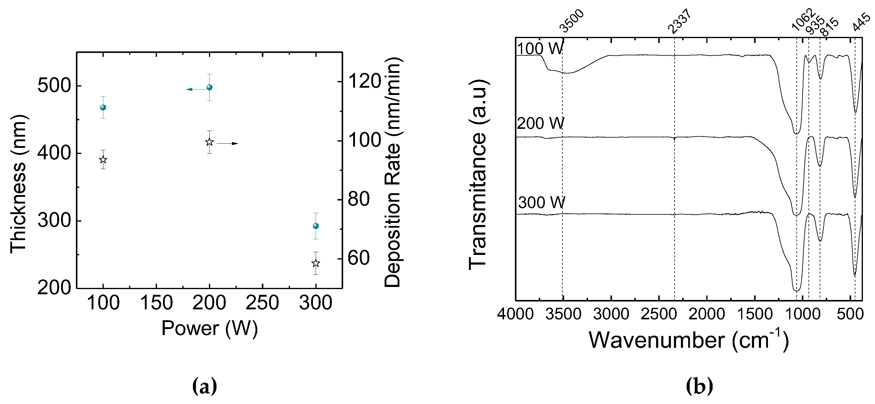
Figure 2.
Si 2p high-resolution XPS peak of films deposited in plasmas of different powers: (a) 100 W, (b) 200 W, (c) 300 W.
Figure 2.
Si 2p high-resolution XPS peak of films deposited in plasmas of different powers: (a) 100 W, (b) 200 W, (c) 300 W.
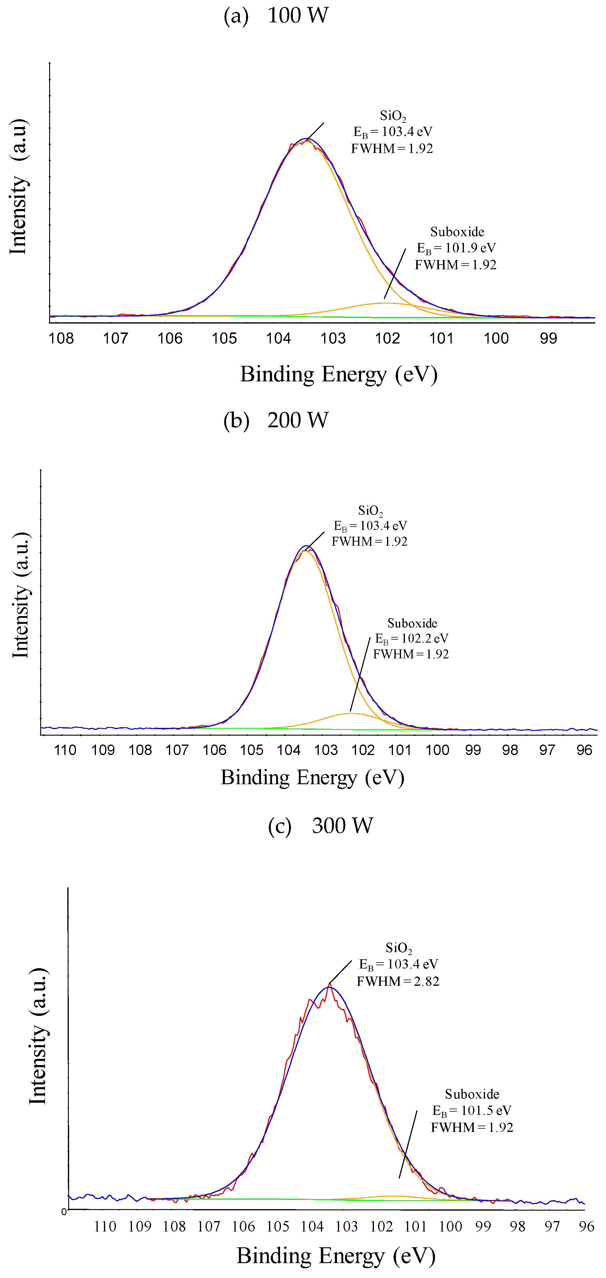
Figure 3.
Schematic illustration of the (a) silicon dioxide group in the tetrahedral configuration and (b) silicon dioxide amorphous structure proposed in the present work. Green highlights detail the silanol moieties and carbon contaminations, as well as the Si-Si crosslinks. Dashed lines indicate binding points with the substrate or adjacent chains.
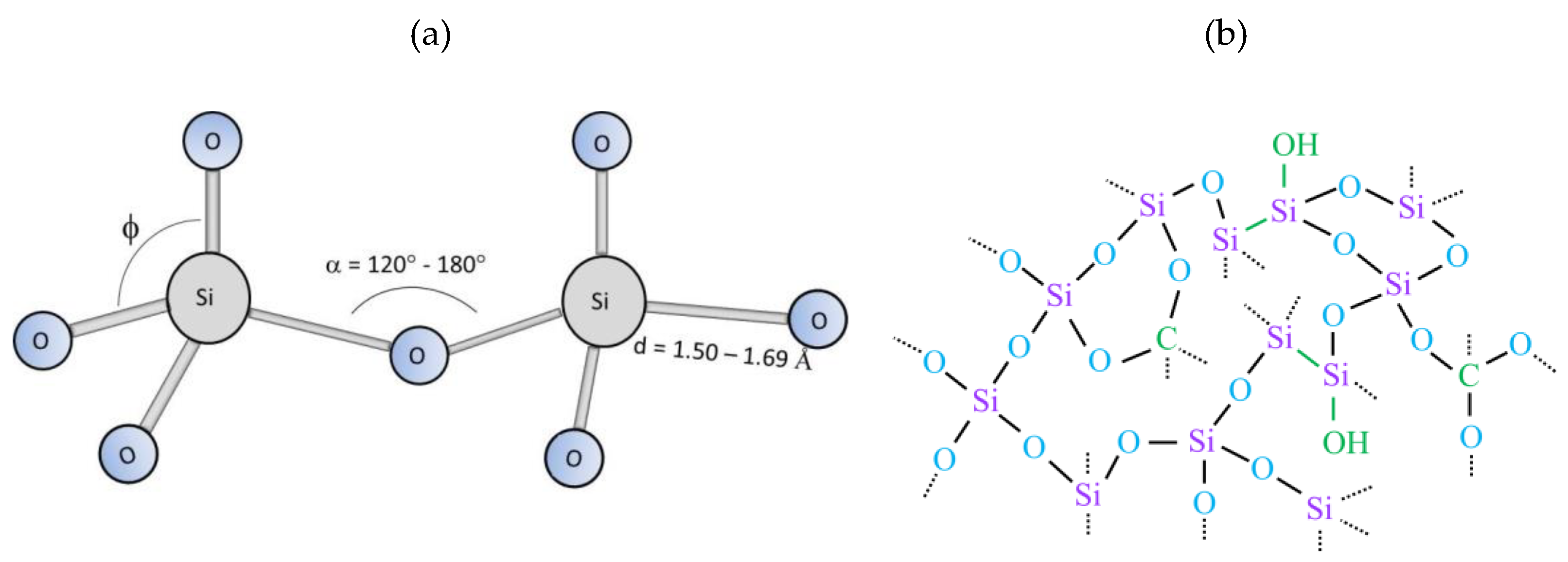
Figure 4.
Two- (left) and three- (right) dimensional surface topographic images (5 μm X 5 μm) of the bare silicon substrate and of the silicon-containing films deposited in plasma of different powers.
Figure 4.
Two- (left) and three- (right) dimensional surface topographic images (5 μm X 5 μm) of the bare silicon substrate and of the silicon-containing films deposited in plasma of different powers.
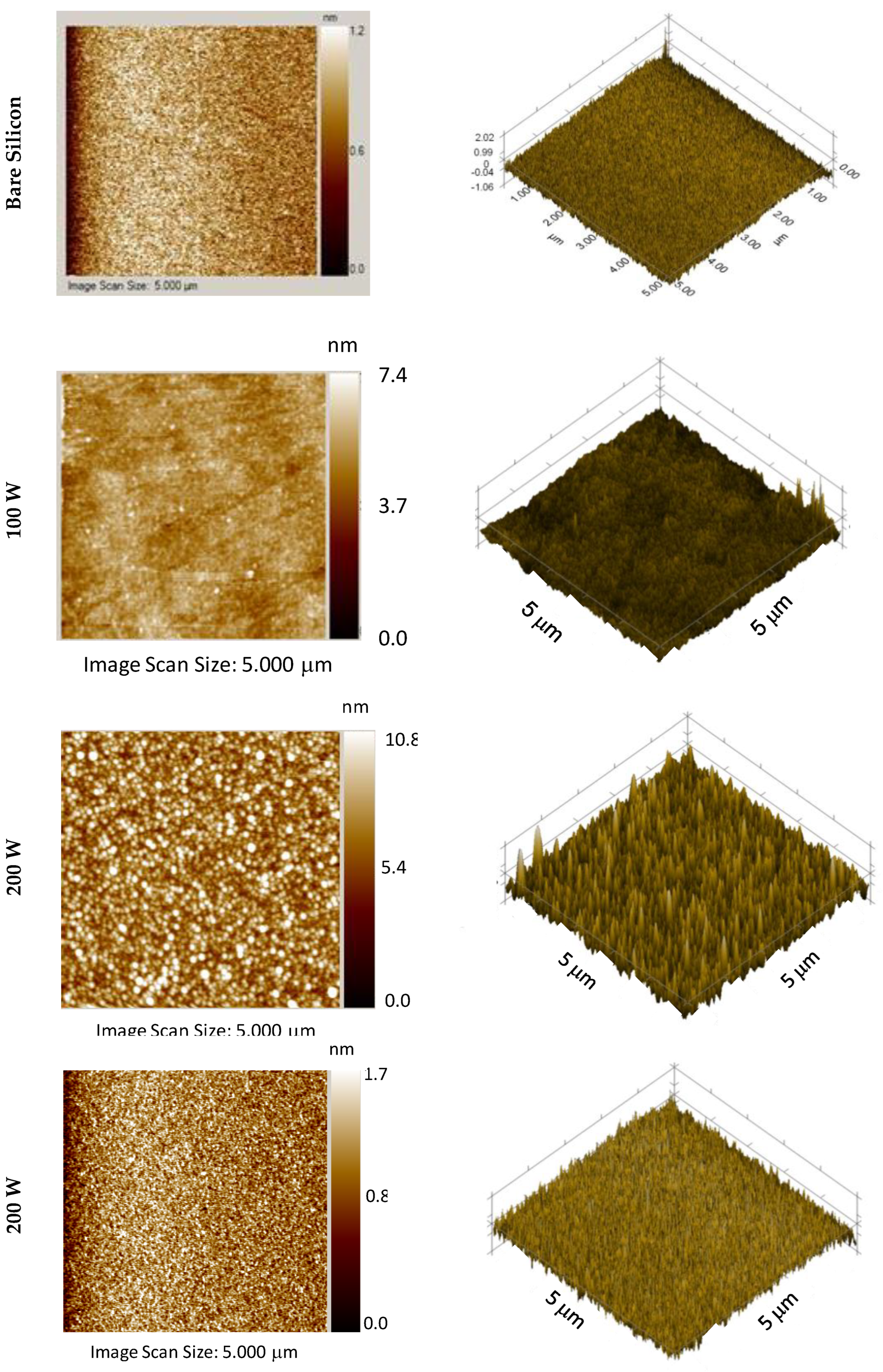
Figure 5.
(a) Root mean square roughness of samples as a function of the plasma excitation power. Dotted line in the graph represents the root mean square roughness values for the bare silicon substrate. (b) Load-displacement curves obtained in nanoindentation experiments from films deposited in plasmas of different powers. A partial unload charge function of 5000 μN was used in the tests.
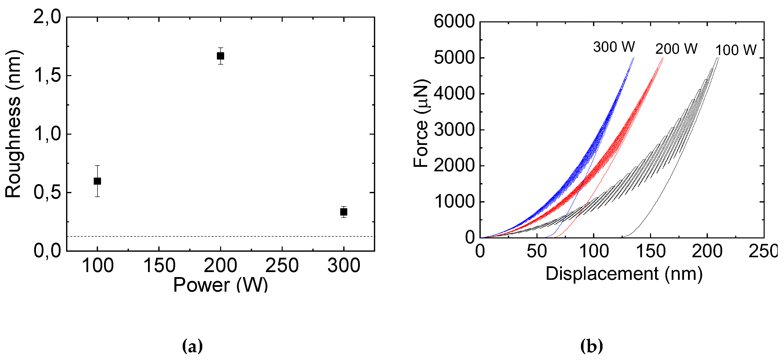
Figure 6.
Atomic force microscopy profiles (a) of the bare silicon and (b – d) of the samples submitted to depositing plasmas of different powers and after indentation with a multiple load function with 5000 µN of maximum force. The inspected area has an extension of 5 μm X 5 μm. In (f) is presented the lateral distance along the indention profile as a function of P.
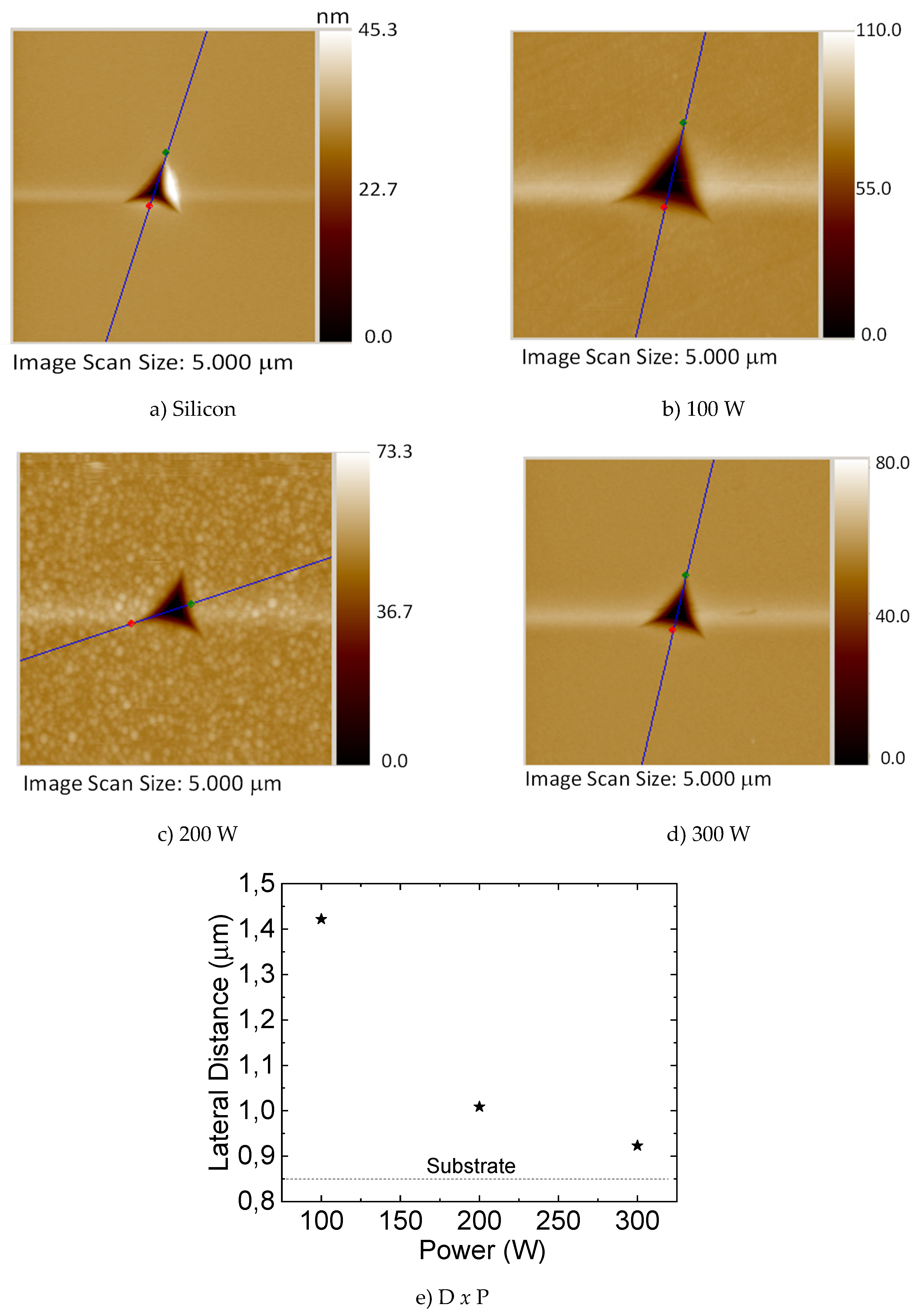
Figure 7.
(a) Hardness and (b) modulus of elasticity of the films as a function of the plasma excitation power. Dashed lines in both graphs represent, respectively, the hardness and the elastic modulus of the bare silicon substrate.
Figure 7.
(a) Hardness and (b) modulus of elasticity of the films as a function of the plasma excitation power. Dashed lines in both graphs represent, respectively, the hardness and the elastic modulus of the bare silicon substrate.
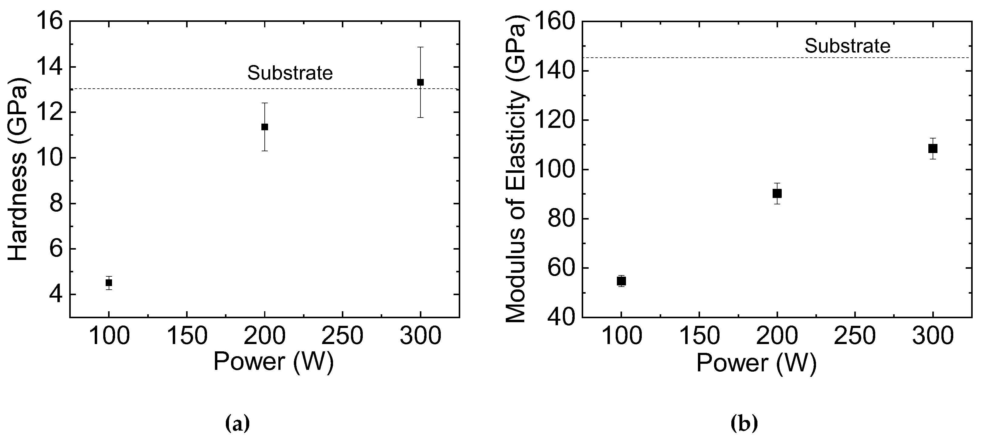
Figure 8.
Optical microscopy images of the surfaces which were submitted to the scratching tests: (a) bare carbon steel substrate and carbon steel exposed to depositing plasmas of (b) 100 W, (c) 200 W and (d) 300 W, after the scratching test using a ramp function with 30 mN of maximum load and 80 µm of extension.
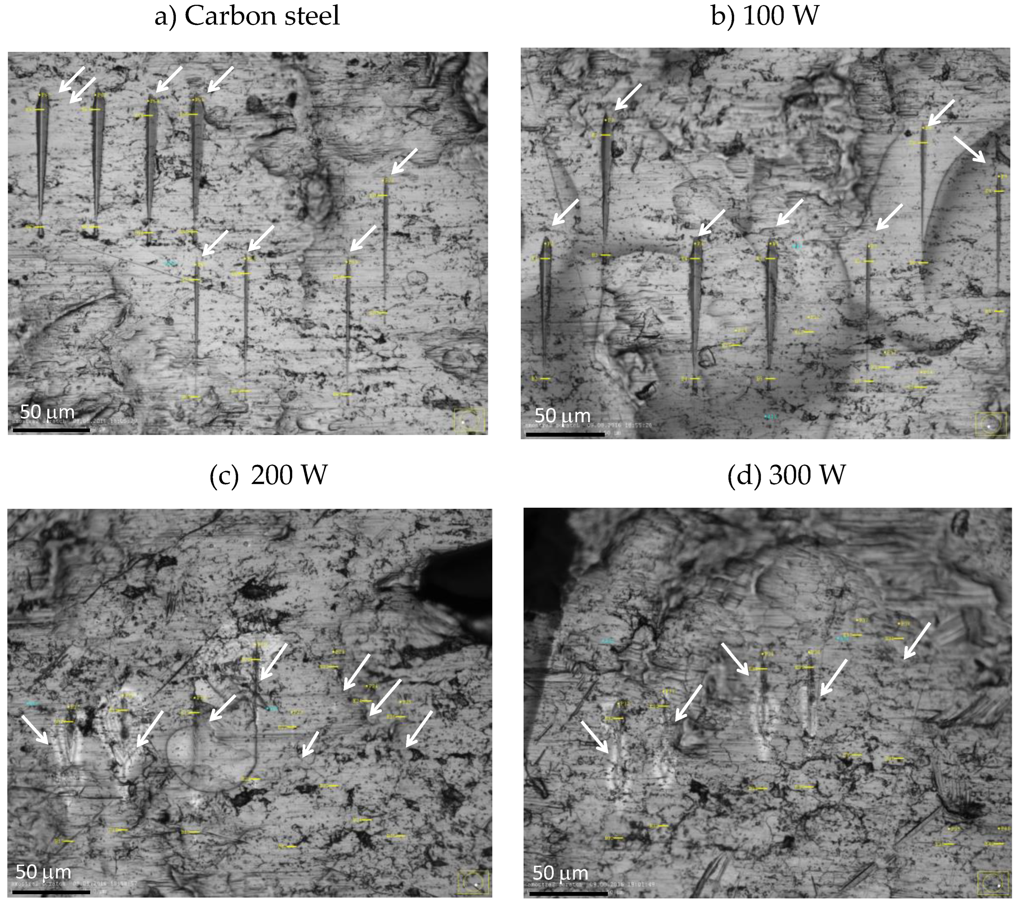
Figure 9.
Atomic force microscopy profiles of the (a) bare silicon substrate and of the silicon exposed to depositing plasmas of (b) 100 W, (c) 200 W and (d) 300 W, after the scratching test using a normal force of 200 μN. The inspected has an extension of 10 μm X 10 μm.
Figure 9.
Atomic force microscopy profiles of the (a) bare silicon substrate and of the silicon exposed to depositing plasmas of (b) 100 W, (c) 200 W and (d) 300 W, after the scratching test using a normal force of 200 μN. The inspected has an extension of 10 μm X 10 μm.
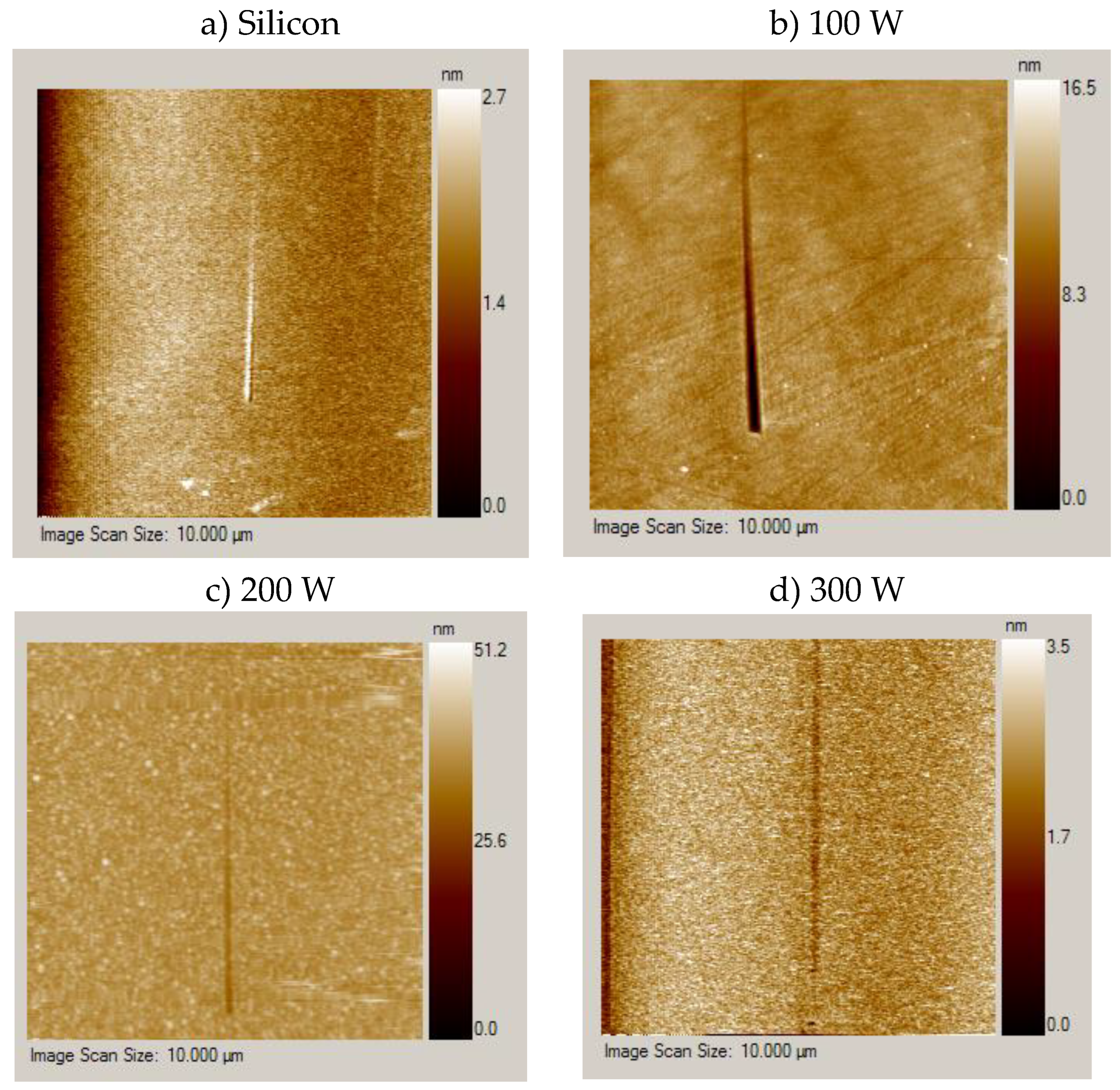
Figure 10.
(a) Potentiodynamic polarization curves for the bare substrate and for the film containing samples. (b) Corrosion current density and potential as a function of the power employed in the plasma deposition process. Dotted and dashed lines indicate the corresponding properties for the bare carbon steel.
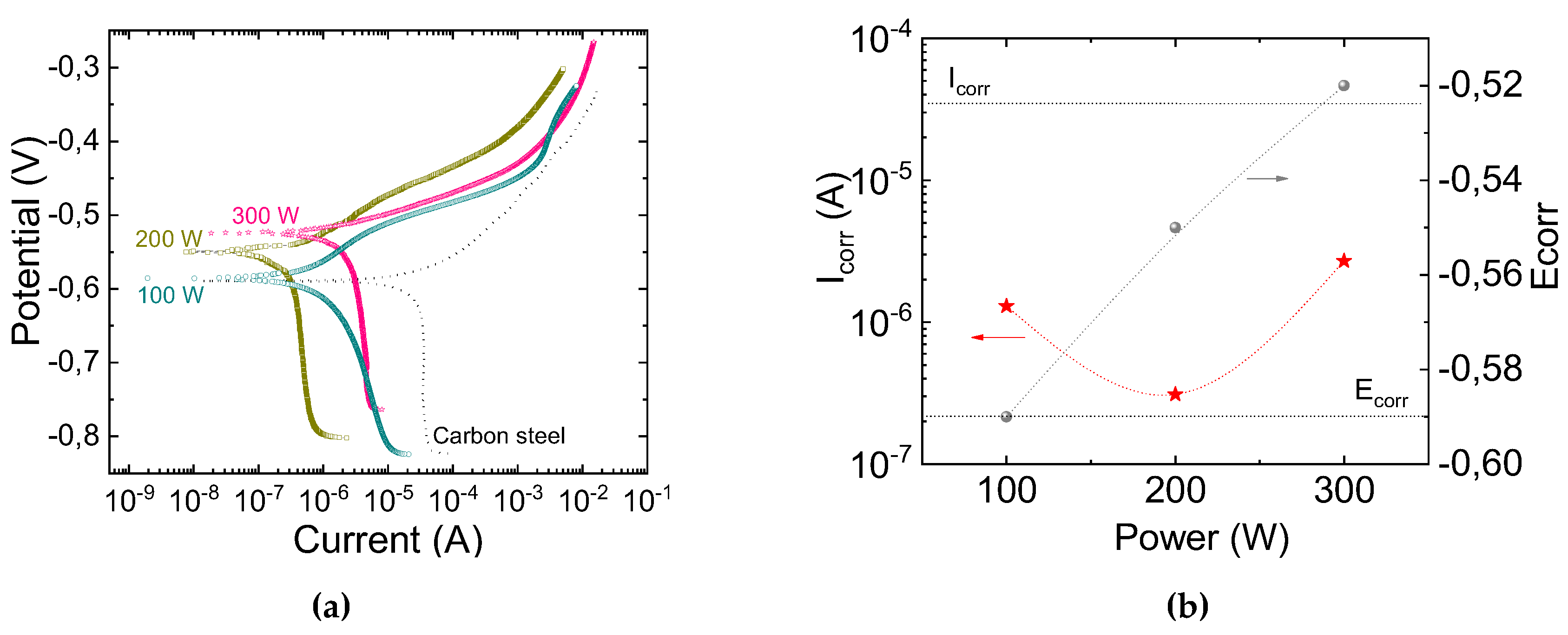

Table 1.
Wavenumber and assignments of the bands detected in the infrared spectra of the films.
| Wavenumbers (cm-1) | Vibrational Modes |
| 445 | Si-O-Si (rocking) |
| 815 | Si-O-Si (bending) |
| 935 | OH in Si-OH (stretching) |
| 1062 | Si-O-Si in SiOx (stretching) |
| 3500 | OH in Si-OH (stretching) |
Table 2.
Atomic proportion of C, O and Si on the surface of the films deposited in plasmas of different excitation powers. The O/Si atomic ratios are also presented.
Table 2.
Atomic proportion of C, O and Si on the surface of the films deposited in plasmas of different excitation powers. The O/Si atomic ratios are also presented.
| Atomic Proportion | ||||
| Plasma Excitation Power (W) | C (% ) | O (% ) | Si (% ) | O/Si |
| 100 | 0.9 | 63.9 | 35.2 | 1.8 |
| 200 | 0.0 | 64.3 | 35.0 | 1.8 |
| 300 | 1.0 | 64.0 | 33.9 | 1.9 |
Table 3.
Proportions of the SiO4 (103.4 eV), SiO2 (102.0 eV) and Si-O (101.5 eV) groups in the total area of the high-resolution Si peak.
Table 3.
Proportions of the SiO4 (103.4 eV), SiO2 (102.0 eV) and Si-O (101.5 eV) groups in the total area of the high-resolution Si peak.
| Plasma Excitation Power (W) | Si-O4 (103.4 eV) |
Si-O2 (102.0 eV) |
Si-O1 (101.5 eV) |
| 100 | 92.3 | 7.7 | - |
| 200 | 91.6 | 8.4 | - |
| 300 | 98.5 | - | 1.5 |
Table 4.
Porosity of the films as a function of P.
| P (W) | Porosity (%) |
| 100 | 0.096 |
| 200 | 0.002 |
| 300 | 0.001 |
Disclaimer/Publisher’s Note: The statements, opinions and data contained in all publications are solely those of the individual author(s) and contributor(s) and not of MDPI and/or the editor(s). MDPI and/or the editor(s) disclaim responsibility for any injury to people or property resulting from any ideas, methods, instructions or products referred to in the content. |
© 2024 by the authors. Licensee MDPI, Basel, Switzerland. This article is an open access article distributed under the terms and conditions of the Creative Commons Attribution (CC BY) license (http://creativecommons.org/licenses/by/4.0/).
Copyright: This open access article is published under a Creative Commons CC BY 4.0 license, which permit the free download, distribution, and reuse, provided that the author and preprint are cited in any reuse.


