1. Introduction
Tungsten diselenide (WSe
2) belongs to a family of van der Waals materials which attract exceptional attention since the isolation of graphene in 2004 [
1] due to their extraordinary electrical, optical and magnetic properties. Being a transition metal dichalcogenide (TMDC), WSe
2 has a layered crystalline structure, where neighboring hexagonal, closely packed monolayers of tungsten and selenium are stacked by weak van der Waals (vdW) forces (see
Figure 1a). The unique material structure of TMDCs leads to their outstanding mechanical properties (exfoliation down to atomically thin flakes [
2,
3]), electronic (electronic structure engineering [
4]) and optical (high refractive index and giant anisotropy [
5,
6]) characteristics, which drive the extensive TMDC research for medical [
7,
8,
9], electronic [
10,
11], optical [
12,
13,
14,
15] and space [
16] scientific communities.
Among a set of common transition metals of TMDCs, tungsten atom is the heaviest one, which sufficiently impacts the WSe
2 properties. For example, the WSe
2 monolayer valence band splitting is three times larger than that for MoS
2 monolayer, which makes it promising for valleytronic and spintronic applications [
17,
18]. Unlike the most TMDC materials [
19,
20,
21,
22], which exhibit n-type conductivity without doping, WSe
2 is hole-conducting and is among the most frequently used p-type 2D materials [
23,
24]. In contrast to WSe
2 single- and few-layered state, its bulk form is much less elaborated in terms of applications, despite the abundance of shapes already reported: nanosheets assembled into nanoflowers [
25], nanotubes [
26], vertically aligned nanosheets [
27] and quantum dots [
28]. Notably, bulk WSe
2, however, has a set of advantageous characteristics for optics, inherited from TMDC material family: a high refractive index
in the visible and infrared spectral ranges, a prominent (20–30%) optical anisotropy, as well as a set of excitonic transitions in visible range at room temperature. Importantly, WSe
2 has a resonant excitonic absorption peak at
nm, which is exceptionally interesting for the photoheating and theranostic applications in NIR-I transparency window of biological tissues. The key issue of exploting the high refractive index of WSe
2 in photonic nanostructures is efficiency and output quality of fabrication methods.
For van der Waals materials, naturally occurring in a layered plane geometry, their shape transformation into spherical nanoparticles is a challenging task[
29]. It was already shown that the femtosecond pulsed laser ablation in liquid (PLAL) approach allows synthesis of spherical vdW NPs, which inherit the crystalline and optical properties of bulk target, demonstrate onion-like or polycrystalline structure and have a broad size distribution from 5 to 250 nm [
30,
31,
32]. For the first time, it was demonstrated for MoS
2 and WS
2 materials[
30,
31], then for MoSe
2 as well[
32]. Interestingly, in case of MoS
2 NPs, the laser fragmentation can be employed to further tune their atomic composition and yield oxidized MoO
3-x NPs[
31]. In the case of MoSe
2 target, the femtosecond ablation revealed the 2H/1T phase transition in NPs[
32].
In our work, we study the possibilities and features of the synthesis of spherical WSe
2 nanoparticles by the femtosecond laser ablation method. Previously, we have successfully used PLAL for preparing NPs of Si [
33], TiN [
34], MoS
2 [
30,
31] and other materials, including core-satellite nanocomposites [
35,
36]. Here, we demonstrate that PLAL yields crystalline WSe
2 NPs with a nearly spherical shape and diameters ranging from
nm up to
nm. Importantly, prepared NPs conserve the high refractive index and excitonic response of an initial bulk WSe
2 target. The latter is illustrated via the photoheating experiments with a tunable Ti:sapphire laser in a wavelength range from 700 nm to 870 nm, which passes through the WSe
2 A-exciton position (
nm). We believe that the proposed high-yield and substrate-free technique will unlock new optical and theranostic applications of WSe
2 NPs.
2. Materials and Methods
2.1. Sample Preparation
Femtosecond pulsed laser ablation in liquids (PLAL) was used to synthesize WSe2 nanoparticles (NPs). A high-purity, synthetically grown bulk WSe2 crystal (2D Semiconductors Inc., dimensions: 1 × 4 × 4 mm) served as the target material. The crystal was placed inside a 10 mL glass vessel filled with 2 mL of DI water. A height of water column above the crystal surface was 10 mm and was kept constant in all experiments. A femtosecond Yb:KGW laser system (TETA-10, Avesta, Moscow, Russia) operating at a wavelength of 1033 nm was employed for the ablation process. The laser delivered pulses with a duration of 270 fs, pulse energy of 100 μJ, and a repetition rate of 1 kHz. The laser beam was focused by a lens with a working distance of 100 mm. The lens-to-crystal distance was carefully adjusted between 95–105 mm to maximize the efficiency of nanoparticle synthesis. Beam scanning in XY plane across the target surface was achieved using two mutually perpendicular linear translation motorized stages, which perform a cyclic sweep of a square pattern at a speed of 5 mm/s. A standard ablation duration was set at 10 minutes. After ablation, the prepared colloidal solutions of WSe2 NPs were collected and analyzed without any further purification or chemical treatment, except differential centrifugation.
2.2. Sample Characterization
Crystalline structure of single NPs was characterized by the high-resolution TEM system (JEM 2010; JEOL) at 200 kV. Drops 2 µl of sample colloids were drop-casted on carbon-coated TEM copper grids and dried at ambient conditions.
A scanning SEM system (MAIA 3; Tescan) with an integrated EDX detector (X-act; Oxford Instruments) was used to examine large NPs shape at inclined view and EDX characterization of the bulk crystal ablation target. Samples were prepared by dropping 2 µl of colloids on a clean Si substrate and drying at ambient conditions.
For SERS measurements drops 20 µl of sample colloids were drop-casted on aluminum surface and spin-coated to get thin films. As-prepared SERS substrates were covered with 2 µl of dye of various concentrations M and dried at ambient conditions during 1 hour. Raman spectroscopy was performed using Horiba LabRAM HR Evolution setup with excitation wavelengths 532 nm and 633 nm, diffraction grating 600 lines/mm and microscope objective 100×, NA 0.9. A good reproducibility of spectra was observed during the measurements.
3. Results and Discussion
3.1. Laser Ablation Synthesis of WSe2 NPs
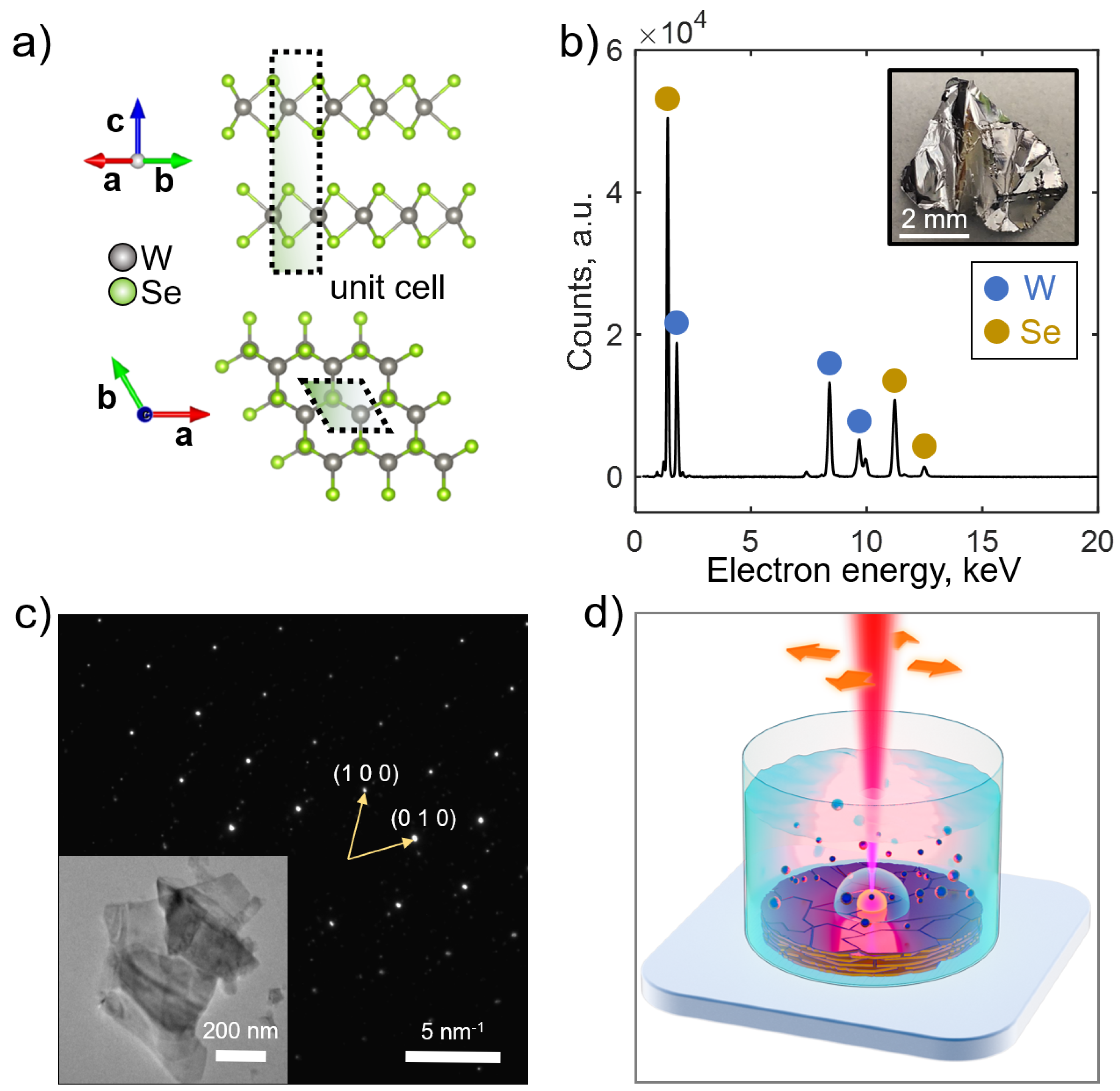
Bulk tungsten diselenide has a layered structure typical for TMDCs materials. Inside every layer tungsten atoms have a trigonal prismatic coordination with regard to selenium, therefore the hexagonal lattice visible from the top is composed of selenium, tungsten and again selenium sandwich planes (see
Figure 1a). A distance between neighboring sandwich layers is
[
37].
Bulk WSe
2 crystal for PLAL was purchased from 2D Semiconductors Inc. The Energy-dispersive X-ray spectroscopy (EDX) of the crystal confirms the stoichiometry quality (
Figure 1b), whereas the selected-area electron diffraction (SAED) of microscopic WSe
2 flake demonstrates a typical hexagonal pattern of monocrystalline TMDCs (
Figure 1c).
The PLAL setup is schematically shown in
Figure 1d. The bulk crystal is placed at the bottom of the glass vessel, filled with DI water. The free surface of the liquid is 1 cm above the top surface of the crystal. Femtosecond laser pulses (1030 nm, 280 fs, 100 μJ) are focused on the bulk crystal surface via the lens (focal distance 100 mm) and generate cavity bubbles with ionized plasma. The plasma cooling and cavity bubbles deflation leads to the plasma condensation into crystalline NPs of different size. The prepared colloid demonstrates a good stability (during at least a month after the synthesis) due to the significant charge of WSe
2 NPs with an electrostatic potential reaching
mV (see Supplementary Note 1).
3.2. Morphology of WSe2 Nanoparticles
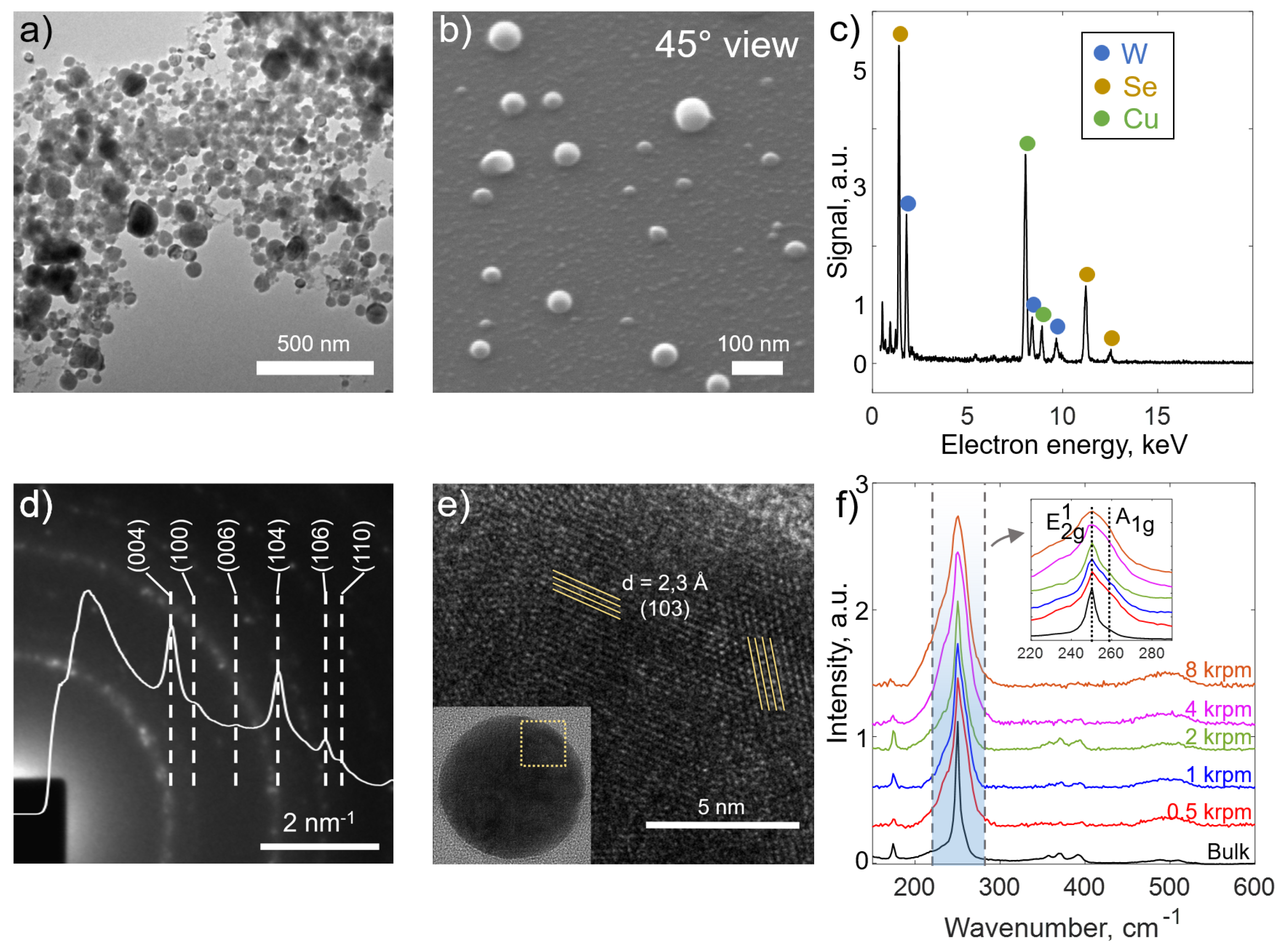
The structural characteristics of WSe
2 nanoparticles synthesized by pulsed laser diffraction (PLAL) in liquids are presented on
Figure 2. Transmission electron microscopy (TEM) image (
Figure 2a) shows the distribution of the nanoparticles. Most of them have a near-spherical morphology. To further confirm that, we performed a tilted Scanning Electron Microscopy (SEM) (
Figure 2b) at an inclination angle of 45 degrees and found that NPs retain a round shape in the image. EDX spectrum (
Figure 1c) confirms that NPs conserve the atomic composition of the original crystal; some additional peaks correspond to the TEM grid copper. SAED pattern (
Figure 1d) reveals distinct diffraction rings, which correspond to the interplanar spacings of crystalline WSe
2. The distances corresponding to the planes (0 0 4), (1 0 0), (0 0 6), (1 0 4), (1 0 6), (1 1 0) are in a good agreement with theoretically calculated values (see Supplementary Materials). High-resolution TEM (HRTEM) of a single WSe
2 NP (
Figure 2e) further confirmes its polycrystalline structure; there are visible zones with different orientations of crystallites. The differential centrifugation of the synthesized colloid was performed in order to separate various average NPs sizes (see the next Section). The fact, that Raman spectra of the as-prepared colloids (
Figure 2f) demonstrate characteristic WSe
2 peak at 250 cm
-1 and generally repeat spectral features of the bulk crystal, indicates the quality of WSe
2 NPs in a broad range of sizes.
3.3. Optical Response of WSe2 Nanoparticles
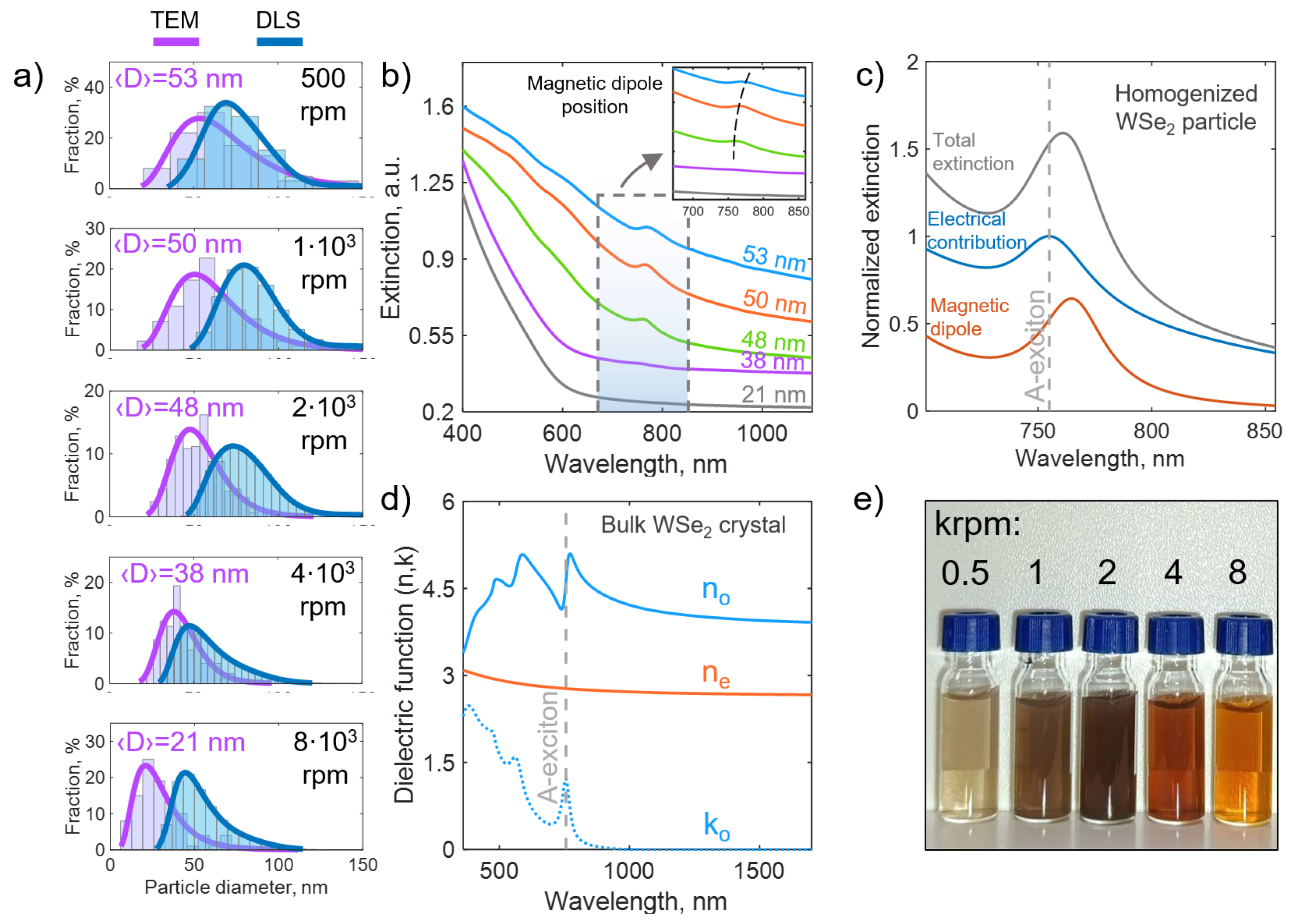
PLAL approach inherently produces a polydisperse colloid. Remarkably, the colloid remained stable for over a month with a negligible aggregation/precipitation, due to a significant negative zeta potential
mV (see Supplementary Information). Given the high refractive index of WSe
2 in the visible spectrum, pronounced changes in optical properties may be achieved due to variations in nanoparticle size. To obtain solutions with different NPs average diameters the initial colloid underwent differential centrifugation. Particle size distributions obtained from manual analysis of TEM images and Dynamic Light Scattering (DLS) measurements confirmed log-normal size distributions, with the average particle size shifting to smaller values with increasing revolutions per minute (rpm). Taking into account that the size distribution of initial colloid is log-normal as well, it leads to different mass concentrations of samples and, consequently, to different colour saturations (transparencies) of the solutions at different centrifugation speeds (
Figure 3e). The most transparent solutions were obtained for lowest and highest centrifugation speeds (see
Figure 3e). Moreover, the difference in solutions hues indicates the difference in extinction properties (see
Figure 3b). Firstly, solutions with smaller NPs possess more rapid extinction fall at shorter wavelength (
), typical for Rayleigh scattering regime. Secondly, the excitonic peak, located at
nm for colloids with smaller average NPs size, is red-shifted for larger NPs (see the inset in
Figure 3b). The presence of the excitonic peak, which originates from the bulk crystal (see
Figure 3d) indicates a NPs crystallinity. The peak shifting is caused by the fact that for WSe
2 NPs large enough (i.e., 130 nm in diameter) the total extinction peak consists of two components (see
Figure 3c): material excitonic feature (visible as a peak in electrical total extinction contribution) and a magnetic dipole resonance (visible in magnetic dipole channel). For WSe
2 NPs large enough the magnetic dipole resonance, as well as other magnetic and electric multipoles, shifts towards longer wavelengths with increasing the particle size, which is an important feature of Mie scattering regime. Thus, the synthesized particles might have applications not only as Rayleigh scatterers, but as Mie-resonators as well after more methodical separation of large WSe
2 NPs.
3.4. Photothermal Applications of WSe2 Nanoparticles
WSe
2 as an efficient absorber in visible and near-IR bands gained much attention as a perspective thin film solar cell absorber [
38,
39,
40]. In this regard, we examine photothermal properties of WSe
2 NPs in visible range at a wavelength of 532 nm, which is readily accessible in our Raman setup and is close to the peak wavelength of solar irradiance at Earth’s surface [
41].
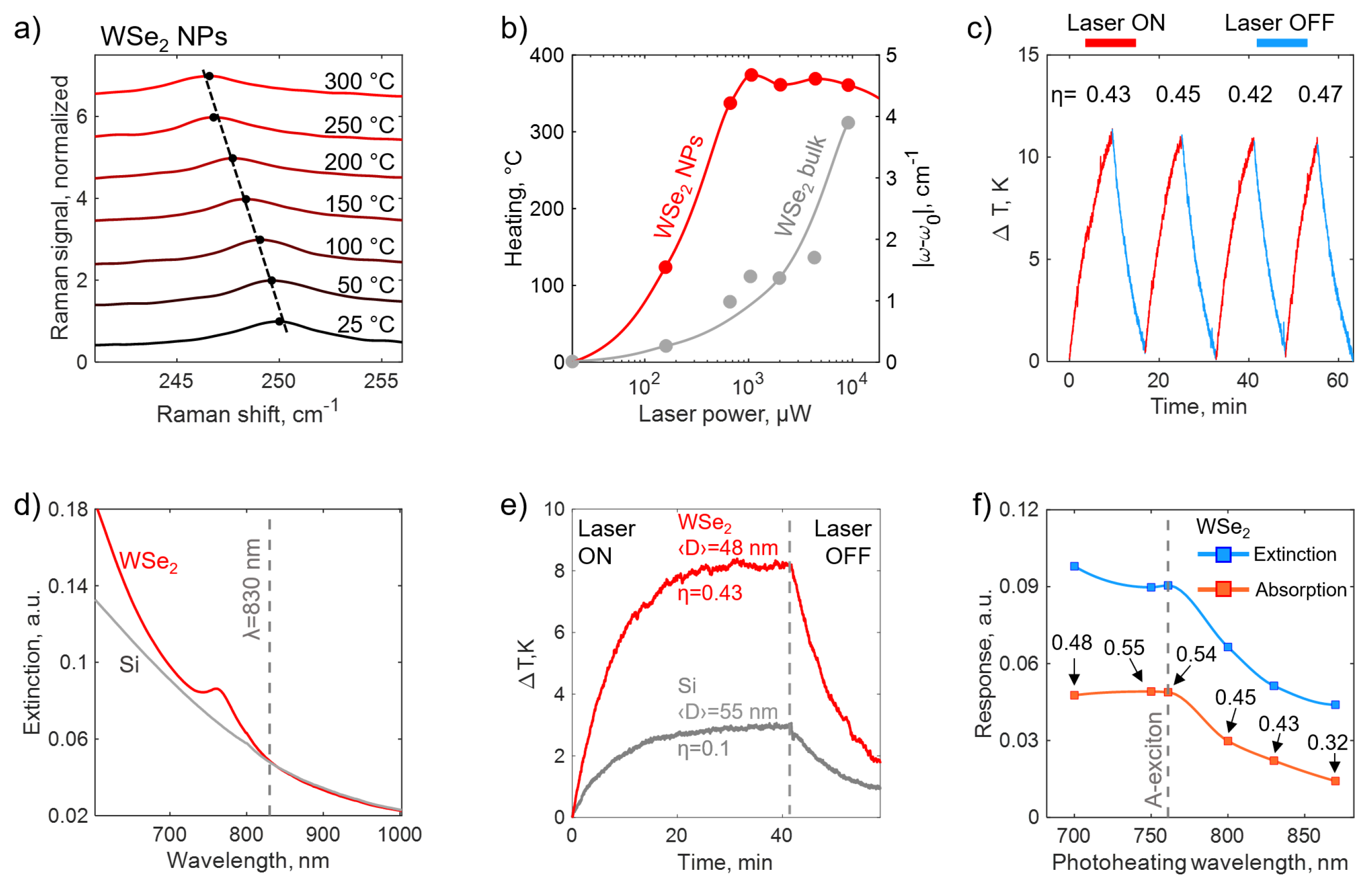
Figure 4a demonstrates a temperature-dependent shift of Raman
peak of WSe
2 NPs, drop-casted on a cover glass substrate, in range from 25 ℃ up to 300 ℃. The sample temperature was monitored via LINKAM temperature control stage, Raman excitation was set 20 μW at 532 nm. We assume a linear dependence of the Raman peak position
on temperature
T due to relatively small temperature range examined in the study:
where
is
peak position at 25 ℃,
is the first-order temperature coefficient, obtained from linear fitting of experimental data from
Figure 4a. The obtained
is within 10% deviation tolerance with values reported in recent works on multilayered WSe
2 flakes[
42,
43] (see Supplementary Materials). Then, we use Eq.
1 to retrieve the local sample temperature from temperature-dependent Raman spectra. The excitation laser 532 nm with different powers was focused into diffraction-limited spot via 100x microscope objective, thus revealing the laser-induced heating efficiency, see
Figure 4b. Interestingly, at quite low irradiation power of 0.7 mW WSe
2 NPs are heated by almost 350 ℃ and therefore have more than 4 times higher photothermal efficiency in comparison with WSe
2 bulk crystal, what originates from an enhanced nanoresonators absorption.
Photothermal antibacterial and cancer therapy nowadays attract a growing attention as a minimally invasive nanomedicine approach. Due to the bacteria inability to adapt and elaborate anti-thermal mechanisms, efficient nanosensitizers are highly required for successive method implementation. Thermal agents should possess a sensitivity to the NIR-I optical window, as well as have a symmetrical (spherical) shape and small (less than 100 nm) size to facilitate their uptake by biological cells. We examine the phototermal response of synthesized crystalline WSe
2 NPs in the NIR-I optical window (700 nm - 980 nm). A collimated beam of 830 nm laser source passes through a cuvette with 1 ml of heated colloid. Solution temperature as a function of time was recorded by thermal imaging camera. Consequent heating-cooling cycles of the same WSe
2 colloid confirmed a good reproducibility of a photothermal conversion coefficient [
44]
(see
Figure 4c). The photothermal response of WSe
2 NPs was compared with Si NPs with the same extinction of water solutions at 830 nm (see
Figure 4d). Due to the presence of excitonic transitions in visible range, which are red-shifted as compared with those in Si, WSe
2 NPs possess higher absorption component in the total extinction cross-section in near-IR (see Supplementary Materials), which results in 4-fold enhancement of the photothermal efficiency, see
Figure 4e.
Photoheating experiments analogous to those presented in
Figure 4e were performed with a tunable titanium-sapphire laser source for wavelengths in range from 700 nm to 870 nm, which includes the WSe
2 A-exciton, see
Figure 4f. Experimentally observed photothermal conversion efficiency
is 0.48 for the shortest utilized wavelength 700 nm, reaches the maximum value of 0.55 close to the excitonic resonance at 750 nm and drops down at longer wavelengths. Colloidal extinction was measured using transmission through a cuvette with a deionized water as a baseline; colloidal absorption curve was obtained by multiplying the values of extinction by
(see Supplementary Materials). This approach allows retrieving colloidal optical absorption properties from photoheating experiments.
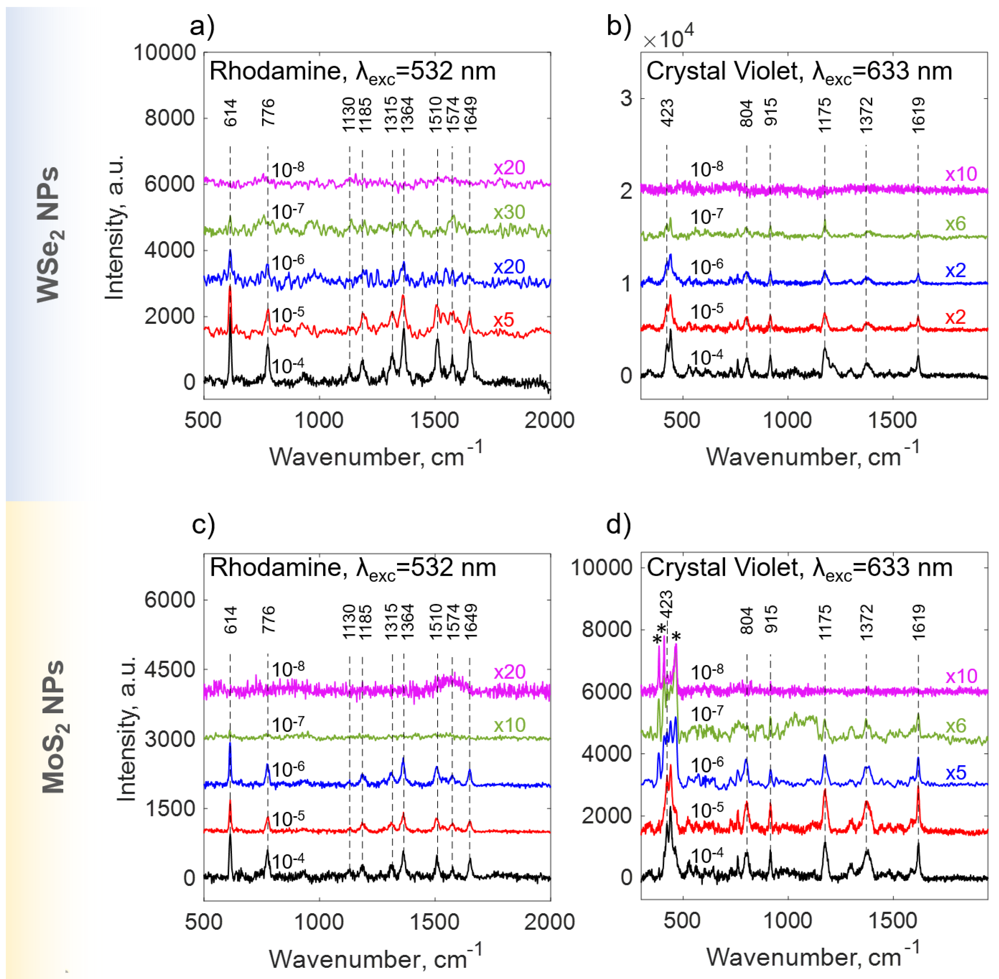
3.5. WSe2 NPs for SERS
Figure 5a,b presents Raman spectra of rhodamine 6G (R6G) and Crystal Violet (CV), respectively, in the concentration range
M which were enhanced by means of WSe
2 substrates.
Raman spectra of R6G molecules acquired from the WSe
2 substrate exhibit strong lines at 614, 776, 1130, 1185, 1315, 1364, 1510, 1574 and 1649 cm
−1 respectively with excitation at 532 nm. All peaks obtained are in good agreement with earlier Raman R6G reports[
45,
46].
Pronounced line on 614 cm
−1 corresponds to the C–C–C ring in-plane bending vibration. The C–H out-of-plane bending vibration for R6G is observed at 776 cm
−1, while the C–H in-plane bending vibration is observed at 1130 cm
−1. The C-O-C stretching frequency appears at 1187 cm
−1. Peaks at 1315, 1364, 1510, 1574, and 1649 cm
−1 correspond to the aromatic C-C stretch of the R6G molecule [
47].
The SERS spectrum of CV contains peaks at 1619 and 1588 cm
−1, which correspond to the C–C stretching vibration of the phenyl ring. The peak at 1372 cm
−1 is the C–C center stretching vibration, and those at 1175 and 804 cm
−1 are C–H bending vibrations. The radical-ring skeletal vibration and C–N bending vibration occur at 915 and 423 cm
−1, respectively [
48,
49].
As expected, the SERS intensity was gradually weakened with decreasing R6G and CV concentration. When the concentration goes down to
M, the R6G and CV peaks can still be detected in range of 400 – 1700 cm
−1 with feeble intensity (see
Figure 5), demonstrating that the detection limit of the WSe
2 substrate has been reached. Current works[
50,
51] approve the high efficiency of SERS sensors based on WSe
2 structures, with LOD values in the range
M.
We perform the analogous SERS experiments on substrates with crystalline MoS
2 NPs, synthesized by the same PLAL approach. Interestingly, nanoparticles from both TMDCs demonstrate a pronounced SERS effect (see
Figure 5). The LOD values for MoS
2 are also moderate (
M), which might be caused by SERS chemical mechanism (CM)[
52]. In
Figure 5d MoS
2 peaks (marked by asterisks) at low dye concentrations
M were observed in the range of 370 – 470 cm
−1 of CV spectra. The MoS
2 modes were identified as
at 385 cm
−1, A
1g at 409 cm
−1, 2LA(M) at 460 cm
−1. The appearance of these spectral lines is caused by a CV signal weakness at low dye concentrations.
In such a way, the possibility to tune the bandgap and optical absorption via the appropriate choice of TMDC NPs, as well as their high colloidal stability[
30] may be desirable in applications.
The obtained structures have scope for improvement. For example, considering particles with a larger specific surface area and more intense absorption at excitation wavelengths may be attractive for SERS. Moreover, Raman signal can be enhanced[
50,
53,
54,
55] by means of creating hybrid structures (TMDC – TMDC) or core – shell / core – satellite structures (TMDCs - Au NPs) with a lower detection threshold.
4. Conclusions
In conclusion, we adapted the femtosecond laser ablation method for the production of WSe
2 NPs from bulk crystal. Importantly, the synthesized NPs retain the crystalline (polycrystalline) structure of the target and inherits the high refractive index and excitonic absorption. The high phototermal response 4 times stronger than that of conventional Si scatterers might be attractive for medical purposes like cancer therapy [
56], whereas the high refractive index and variety of accessible sizes unblocks WSe
2 NPs for Mie-tronics [
57]. Generally, highly symmetrical, nano-sized, crystalline and highly refractive NPs are promising for various applications in postsilicon nanotechnologies.
Author Contributions
Conceptualization, A.B., A.A. and V.v.; methodology, G.Ts., A.K. and A.U.; validation, A.A., A.P. and A.I.; formal analysis, I.K., G.E. and A.V.; investigation, D.D., I.M., D.Y., A.S., G.T., D.Ts., N.B. and A.U.; resources, A.C., D.G. and A.M.; data curation, I.K., A.U. and N.B.; writing—original draft preparation, A.U., D.D. and I.K.; writing—review and editing, A.B. and A.V.; visualization, A.U.; supervision, A.B., A.A. and V.V.; project administration, A.U.; funding acquisition, A.A., A.B. and V.V.; All authors have read and agreed to the published version of the manuscript.
Funding
This research was funded by the Ministry of Science and Higher Education of the Russian Federation, agreement 075-15-2024-560
Data Availability Statement
The original contributions presented in the study are included in the article and Supplementary Materials; further inquiries can be directed to the corresponding author.
Acknowledgments
The authors acknowledge Dr. Valentyn Solovey for the graphical illustration of the PLAL setup.
Conflicts of Interest
The authors declare no conflicts of interest.
Abbreviations
The following abbreviations are used in this manuscript:
| TMDC |
Transition Metal Dichalcogenide |
| NP |
Nanoparticle |
| PLAL |
Pulsed Laser Ablation in Liquid |
| SEM |
Scanning Electron Microscope |
| TEM |
Transmission Electron Microscope |
| SAED |
Selected Area Electron Diffraction |
| EDX |
Energy-dispersive X-ray spectroscopy |
| SERS |
Surface-Enhanced Raman Scattering |
| R6G |
Rhodamine 6G |
| CV |
Crystal Violet |
References
- Novoselov, K.S.; Geim, A.K.; Morozov, S.V.; Jiang, D.e.; Zhang, Y.; Dubonos, S.V.; Grigorieva, I.V.; Firsov, A.A. Electric field effect in atomically thin carbon films. science 2004, 306, 666–669. [Google Scholar] [CrossRef] [PubMed]
- Hossen, M.F.; Shendokar, S.; Aravamudhan, S. Defects and Defect Engineering of Two-Dimensional Transition Metal Dichalcogenide (2D TMDC) Materials. Nanomaterials 2024, 14, 410. [Google Scholar] [CrossRef]
- Falin, A.; Holwill, M.; Lv, H.; Gan, W.; Cheng, J.; Zhang, R.; Qian, D.; Barnett, M.R.; Santos, E.J.; Novoselov, K.S.; et al. Mechanical properties of atomically thin tungsten dichalcogenides: WS2, WSe2, and WTe2. ACS nano 2021, 15, 2600–2610. [Google Scholar] [CrossRef] [PubMed]
- Zhao, Y.H.; Yang, F.; Wang, J.; Guo, H.; Ji, W. Continuously tunable electronic structure of transition metal dichalcogenides superlattices. Scientific Reports 2015, 5, 8356. [Google Scholar] [CrossRef] [PubMed]
- Ermolaev, G.A.; Stebunov, Y.V.; Vyshnevyy, A.A.; Tatarkin, D.E.; Yakubovsky, D.I.; Novikov, S.M.; Baranov, D.G.; Shegai, T.; Nikitin, A.Y.; Arsenin, A.V.; et al. Broadband optical properties of monolayer and bulk MoS2. npj 2D Materials and Applications 2020, 4, 21. [Google Scholar] [CrossRef]
- Ermolaev, G.; Grudinin, D.; Stebunov, Y.; Voronin, K.V.; Kravets, V.; Duan, J.; Mazitov, A.; Tselikov, G.; Bylinkin, A.; Yakubovsky, D.; et al. Giant optical anisotropy in transition metal dichalcogenides for next-generation photonics. Nature communications 2021, 12, 854. [Google Scholar] [CrossRef]
- Lin, T.; Zhong, L.; Guo, L.; Fu, F.; Chen, G. Seeing diabetes: visual detection of glucose based on the intrinsic peroxidase-like activity of MoS 2 nanosheets. Nanoscale 2014, 6, 11856–11862. [Google Scholar] [CrossRef]
- Fusco, L.; Gazzi, A.; Peng, G.; Shin, Y.; Vranic, S.; Bedognetti, D.; Vitale, F.; Yilmazer, A.; Feng, X.; Fadeel, B.; et al. Graphene and other 2D materials: a multidisciplinary analysis to uncover the hidden potential as cancer theranostics. Theranostics 2020, 10, 5435. [Google Scholar] [CrossRef]
- Anju, S.; Mohanan, P. Biomedical applications of transition metal dichalcogenides (TMDCs). Synthetic Metals 2021, 271, 116610. [Google Scholar] [CrossRef]
- Jiang, D.; Liu, Z.; Xiao, Z.; Qian, Z.; Sun, Y.; Zeng, Z.; Wang, R. Flexible electronics based on 2D transition metal dichalcogenides. Journal of Materials Chemistry A 2022, 10, 89–121. [Google Scholar] [CrossRef]
- Kang, T.; Tang, T.W.; Pan, B.; Liu, H.; Zhang, K.; Luo, Z. Strategies for controlled growth of transition metal dichalcogenides by chemical vapor deposition for integrated electronics. ACS materials Au 2022, 2, 665–685. [Google Scholar] [CrossRef] [PubMed]
- Verre, R.; Baranov, D.G.; Munkhbat, B.; Cuadra, J.; Käll, M.; Shegai, T. Transition metal dichalcogenide nanodisks as high-index dielectric Mie nanoresonators. Nature nanotechnology 2019, 14, 679–683. [Google Scholar] [CrossRef] [PubMed]
- Munkhbat, B.; Küçüköz, B.; Baranov, D.G.; Antosiewicz, T.J.; Shegai, T.O. Nanostructured transition metal dichalcogenide multilayers for advanced nanophotonics. Laser & Photonics Reviews 2023, 17, 2200057. [Google Scholar]
- Ermolaev, G.; Grudinin, D.; Voronin, K.; Vyshnevyy, A.; Arsenin, A.; Volkov, V. Van der Waals materials for subdiffractional light guidance. Photonics 2022, 9, 744. [Google Scholar] [CrossRef]
- Stuhrenberg, M.; Munkhbat, B.; Baranov, D.G.; Cuadra, J.; Yankovich, A.B.; Antosiewicz, T.J.; Olsson, E.; Shegai, T. Strong light–matter coupling between plasmons in individual gold bi-pyramids and excitons in mono-and multilayer WSe2. Nano letters 2018, 18, 5938–5945. [Google Scholar] [CrossRef] [PubMed]
- Roy, S.; Bermel, P. Tungsten-disulfide-based ultrathin solar cells for space applications. IEEE Journal of Photovoltaics 2022, 12, 1184–1191. [Google Scholar] [CrossRef]
- Xiao, D.; Liu, G.B.; Feng, W.; Xu, X.; Yao, W. Coupled spin and valley physics in monolayers of MoS 2 and other group-VI dichalcogenides. Physical review letters 2012, 108, 196802. [Google Scholar] [CrossRef]
- Yuan, H.; Bahramy, M.S.; Morimoto, K.; Wu, S.; Nomura, K.; Yang, B.J.; Shimotani, H.; Suzuki, R.; Toh, M.; Kloc, C.; et al. Zeeman-type spin splitting controlled by an electric field. Nature Physics 2013, 9, 563–569. [Google Scholar] [CrossRef]
- Quereda, J.; Ghiasi, T.S.; You, J.S.; van den Brink, J.; van Wees, B.J.; van der Wal, C.H. Symmetry regimes for circular photocurrents in monolayer MoSe2. Nature communications 2018, 9, 3346. [Google Scholar] [CrossRef]
- Lundt, N.; Cherotchenko, E.; Iff, O.; Fan, X.; Shen, Y.; Bigenwald, P.; Kavokin, A.; Höfling, S.; Schneider, C. The interplay between excitons and trions in a monolayer of MoSe2. Applied Physics Letters 2018, 112. [Google Scholar] [CrossRef]
- Liu, Y.; Hu, X.; Wang, T.; Liu, D. Reduced binding energy and layer-dependent exciton dynamics in monolayer and multilayer WS2. ACS nano 2019, 13, 14416–14425. [Google Scholar] [CrossRef] [PubMed]
- Blackburn, J.L.; Zhang, H.; Myers, A.R.; Dunklin, J.R.; Coffey, D.C.; Hirsch, R.N.; Vigil-Fowler, D.; Yun, S.J.; Cho, B.W.; Lee, Y.H.; et al. Measuring photoexcited free charge carriers in mono-to few-layer transition-metal dichalcogenides with steady-state microwave conductivity. The Journal of Physical Chemistry Letters 2019, 11, 99–107. [Google Scholar] [CrossRef] [PubMed]
- Zhao, P.; Kiriya, D.; Azcatl, A.; Zhang, C.; Tosun, M.; Liu, Y.S.; Hettick, M.; Kang, J.S.; McDonnell, S.; Kc, S.; et al. Air stable p-doping of WSe2 by covalent functionalization. ACS nano 2014, 8, 10808–10814. [Google Scholar] [CrossRef] [PubMed]
- Cheng, Q.; Pang, J.; Sun, D.; Wang, J.; Zhang, S.; Liu, F.; Chen, Y.; Yang, R.; Liang, N.; Lu, X.; et al. WSe2 2D p-type semiconductor-based electronic devices for information technology: design, preparation, and applications. InfoMat 2020, 2, 656–697. [Google Scholar] [CrossRef]
- Sokolikova, M.S.; Sherrell, P.C.; Palczynski, P.; Bemmer, V.L.; Mattevi, C. Direct solution-phase synthesis of 1T’WSe2 nanosheets. Nature communications 2019, 10, 712. [Google Scholar] [CrossRef]
- Xu, K.; Wang, F.; Wang, Z.; Zhan, X.; Wang, Q.; Cheng, Z.; Safdar, M.; He, J. Component-controllable WS2 (1–x) Se2 x nanotubes for efficient hydrogen evolution reaction. ACS nano 2014, 8, 8468–8476. [Google Scholar] [CrossRef]
- Sierra-Castillo, A.; Haye, E.; Acosta, S.; Bittencourt, C.; Colomer, J.F. Synthesis and characterization of highly crystalline vertically aligned WSe2 nanosheets. Applied Sciences 2020, 10, 874. [Google Scholar] [CrossRef]
- Azam, A.; Yang, J.; Li, W.; Huang, J.K.; Li, S. Tungsten diselenides (WSe2) quantum dots: Fundamental, properties, synthesis and applications. Progress in Materials Science 2023, 132, 101042. [Google Scholar] [CrossRef]
- Ye, F.; Musselman, K.P. Synthesis of low dimensional nanomaterials by pulsed laser ablation in liquid. APL Materials 2024, 12. [Google Scholar] [CrossRef]
- Tselikov, G.I.; Ermolaev, G.A.; Popov, A.A.; Tikhonowski, G.V.; Panova, D.A.; Taradin, A.S.; Vyshnevyy, A.A.; Syuy, A.V.; Klimentov, S.M.; Novikov, S.M.; et al. Transition metal dichalcogenide nanospheres for high-refractive-index nanophotonics and biomedical theranostics. Proceedings of the National Academy of Sciences 2022, 119, e2208830119. [Google Scholar] [CrossRef]
- Chernikov, A.S.; Tselikov, G.I.; Gubin, M.Y.; Shesterikov, A.V.; Khorkov, K.S.; Syuy, A.V.; Ermolaev, G.A.; Kazantsev, I.S.; Romanov, R.I.; Markeev, A.M.; et al. Tunable optical properties of transition metal dichalcogenide nanoparticles synthesized by femtosecond laser ablation and fragmentation. Journal of Materials Chemistry C 2023, 11, 3493–3503. [Google Scholar] [CrossRef]
- Ye, F.; Ayub, A.; Karimi, R.; Wettig, S.; Sanderson, J.; Musselman, K.P. Defect-Rich MoSe2 2H/1T Hybrid Nanoparticles Prepared from Femtosecond Laser Ablation in Liquid and Their Enhanced Photothermal Conversion Efficiencies. Advanced Materials 2023, 35, 2301129. [Google Scholar] [CrossRef] [PubMed]
- Al-Kattan, A.; Nirwan, V.P.; Popov, A.; Ryabchikov, Y.V.; Tselikov, G.; Sentis, M.; Fahmi, A.; Kabashin, A.V. Recent advances in laser-ablative synthesis of bare Au and Si nanoparticles and assessment of their prospects for tissue engineering applications. International Journal of Molecular Sciences 2018, 19, 1563. [Google Scholar] [CrossRef] [PubMed]
- Popov, A.A.; Tselikov, G.; Dumas, N.; Berard, C.; Metwally, K.; Jones, N.; Al-Kattan, A.; Larrat, B.; Braguer, D.; Mensah, S.; et al. Laser-synthesized TiN nanoparticles as promising plasmonic alternative for biomedical applications. Scientific reports 2019, 9, 1194. [Google Scholar] [CrossRef] [PubMed]
- Popov, A.A.; Swiatkowska-Warkocka, Z.; Marszalek, M.; Tselikov, G.; Zelepukin, I.V.; Al-Kattan, A.; Deyev, S.M.; Klimentov, S.M.; Itina, T.E.; Kabashin, A.V. Laser-ablative synthesis of ultrapure magneto-plasmonic core-satellite nanocomposites for biomedical applications. Nanomaterials 2022, 12, 649. [Google Scholar] [CrossRef]
- Al-Kattan, A.; Tselikov, G.; Metwally, K.; Popov, A.A.; Mensah, S.; Kabashin, A.V. Laser ablation-assisted synthesis of plasmonic Si@ Au core-satellite nanocomposites for biomedical applications. Nanomaterials 2021, 11, 592. [Google Scholar] [CrossRef]
- Voß, D.; Krüger, P.; Mazur, A.; Pollmann, J. Atomic and electronic structure of WSe 2 from ab initio theory: Bulk crystal and thin film systems. Physical Review B 1999, 60, 14311. [Google Scholar] [CrossRef]
- Neilson, K.M.; Hamtaei, S.; Nassiri Nazif, K.; Carr, J.M.; Rahimisheikh, S.; Nitta, F.U.; Brammertz, G.; Blackburn, J.L.; Hadermann, J.; Saraswat, K.C.; et al. Toward Mass Production of Transition Metal Dichalcogenide Solar Cells: Scalable Growth of Photovoltaic-Grade Multilayer WSe2 by Tungsten Selenization. ACS nano 2024, 18, 24819–24828. [Google Scholar] [CrossRef]
- Nassiri Nazif, K.; Nitta, F.U.; Daus, A.; Saraswat, K.C.; Pop, E. Efficiency limit of transition metal dichalcogenide solar cells. Communications Physics 2023, 6, 367. [Google Scholar] [CrossRef]
- Rahman, M.A. Performance analysis of WSe2-based bifacial solar cells with different electron transport and hole transport materials by SCAPS-1D. Heliyon 2022, 8. [Google Scholar]
- Wang, L.; Yu, J. Chapter 1 - Principles of photocatalysis. In S-scheme Heterojunction Photocatalysts; Yu, J.; Zhang, L.; Wang, L.; Zhu, B., Eds.; Elsevier, 2023; Vol. 35, Interface Science and Technology, pp. 1–52. [CrossRef]
- Easy, E.; Gao, Y.; Wang, Y.; Yan, D.; Goushehgir, S.M.; Yang, E.H.; Xu, B.; Zhang, X. Experimental and computational investigation of layer-dependent thermal conductivities and interfacial thermal conductance of one-to three-layer WSe2. ACS Applied Materials & Interfaces 2021, 13, 13063–13071. [Google Scholar]
- Li, Z.; Wang, Y.; Jiang, J.; Liang, Y.; Zhong, B.; Zhang, H.; Yu, K.; Kan, G.; Zou, M. Temperature-dependent Raman spectroscopy studies of 1–5-layer WSe2. Nano Research 2020, 13, 591–595. [Google Scholar] [CrossRef]
- Abu Serea, E.S.; Orue, I.; Garcia, J.A.; Lanceros-Mendez, S.; Reguera, J. Enhancement and tunability of plasmonic-magnetic hyperthermia through shape and size control of Au: fe3O4 janus nanoparticles. ACS Applied Nano Materials 2023, 6, 18466–18479. [Google Scholar] [CrossRef]
- He, X.N.; Gao, Y.; Mahjouri-Samani, M.; Black, P.; Allen, J.; Mitchell, M.; Xiong, W.; Zhou, Y.; Jiang, L.; Lu, Y. Surface-enhanced Raman spectroscopy using gold-coated horizontally aligned carbon nanotubes. Nanotechnology 2012, 23, 205702. [Google Scholar] [CrossRef] [PubMed]
- Sil, S.; Kuhar, N.; Acharya, S.; Umapathy, S. Is chemically synthesized graphene ‘really’a unique substrate for SERS and fluorescence quenching? Scientific Reports 2013, 3, 3336. [Google Scholar] [CrossRef]
- Watanabe, H.; Hayazawa, N.; Inouye, Y.; Kawata, S. DFT vibrational calculations of rhodamine 6G adsorbed on silver: analysis of tip-enhanced Raman spectroscopy. The Journal of Physical Chemistry B 2005, 109, 5012–5020. [Google Scholar] [CrossRef]
- Meng, W.; Hu, F.; Jiang, X.; Lu, L. Preparation of silver colloids with improved uniformity and stable surface-enhanced Raman scattering. Nanoscale research letters 2015, 10, 1–8. [Google Scholar] [CrossRef]
- Lai, K.; Zhang, Y.; Du, R.; Zhai, F.; Rasco, B.A.; Huang, Y. Determination of chloramphenicol and crystal violet with surface enhanced Raman spectroscopy. Sensing and Instrumentation for Food Quality and Safety 2011, 5, 19–24. [Google Scholar] [CrossRef]
- Jebakumari, K.E.; Murugasenapathi, N.; Palanisamy, T. Engineered two-dimensional nanostructures as SERS substrates for biomolecule sensing: A review. Biosensors 2023, 13, 102. [Google Scholar] [CrossRef]
- Lv, Q.; Tan, J.; Wang, Z.; Yu, L.; Liu, B.; Lin, J.; Li, J.; Huang, Z.H.; Kang, F.; Lv, R. Femtomolar-level molecular sensing of monolayer tungsten diselenide induced by heteroatom doping with long-term stability. Advanced Functional Materials 2022, 32, 2200273. [Google Scholar] [CrossRef]
- Le Ru, E.; Etchegoin, P. Principles of Surface-Enhanced Raman Spectroscopy: and related plasmonic effects; Elsevier, 2008.
- Majumdar, D.; Jana, S.; Ray, S.K. Gold nanoparticles decorated 2D-WSe2 as a SERS substrate. Spectrochimica Acta Part A: Molecular and Biomolecular Spectroscopy 2022, 278, 121349. [Google Scholar] [CrossRef] [PubMed]
- Chen, M.; Liu, D.; Du, X.; Lo, K.H.; Wang, S.; Zhou, B.; Pan, H. 2D materials: Excellent substrates for surface-enhanced Raman scattering (SERS) in chemical sensing and biosensing. TrAC Trends in Analytical Chemistry 2020, 130, 115983. [Google Scholar] [CrossRef]
- Tang, X.; Hao, Q.; Hou, X.; Lan, L.; Li, M.; Yao, L.; Zhao, X.; Ni, Z.; Fan, X.; Qiu, T. Exploring and Engineering 2D Transition Metal Dichalcogenides toward Ultimate SERS Performance. Advanced Materials 2024, 2312348. [Google Scholar] [CrossRef] [PubMed]
- Zograf, G.P.; Petrov, M.I.; Makarov, S.V.; Kivshar, Y.S. All-dielectric thermonanophotonics. Advances in Optics and Photonics 2021, 13, 643–702. [Google Scholar] [CrossRef]
- Kivshar, Y. The rise of Mie-tronics, 2022.
|
Disclaimer/Publisher’s Note: The statements, opinions and data contained in all publications are solely those of the individual author(s) and contributor(s) and not of MDPI and/or the editor(s). MDPI and/or the editor(s) disclaim responsibility for any injury to people or property resulting from any ideas, methods, instructions or products referred to in the content. |
© 2024 by the authors. Licensee MDPI, Basel, Switzerland. This article is an open access article distributed under the terms and conditions of the Creative Commons Attribution (CC BY) license (http://creativecommons.org/licenses/by/4.0/).