
Submitted:
11 November 2024
Posted:
12 November 2024
You are already at the latest version
Abstract
Two-dimensional materials with nanostructure have been introduced as promising candidates for SERS platform for sensing application. However, dynamic control and tuning SERS remains a long-standing problem. Here, we demonstrated active tuning of enhancement factor of the first and second-order Raman mode of monolayer(1L) MoS2 transferred onto flexible metallic nanotip array. Using mechanical strain, the enhancement factor of 1L MoS2/nanotip is modulated from 1.23 to 8.72 for 2LA mode. For the same mode, the SERS intensity is enhanced by ~31 times when silver nanoparticles of ~10 nm diameter are deposited on 1L MoS2/nanotip, which is tuned up to ~ 34 times by compressive strain. The change in SERS enhancement factor is due to the decrease (increase) in gap-width as the sample is bent inwardly (outwardly). This is corroborated by FEM structural and electromagnetic simulation. We also observed significant control over mode peak and linewidth, which may find application in biosensing, chemical detetction, optoelectronics.
Keywords:
Tunable SERS
; multi-order Raman scattering
; MoS2
; flexible nano-tip
; enhancement factor
1. Introduction
Surface enhanced Raman scattering (SERS) is an enhanced version of Raman scattering enabled by metallic nanostructure. It is now well documented that enhanced Raman signal i.e., SERS is attributed to electromagnetic and chemical enhancement. While the chemical enhancement mainly comes from the interaction between the molecule and metallic substrate, the architecture of the substrates plays an important role towards electromagnetic enhancement[1,2]. Metallic nanostructure decorated substrate[3] such as nanospheres or nanoparticles[4,5], nanorods[5,6], nanowires[6], nano-stars[7,8], nanoscale roughened films[9,10] have enabled application in biosensing[11,12], pesticide detection[13], chemical analysis[14]. Apart from metallic nanostructure, plasmonic structures such as nanogap have also shown great SERS enhancement[15,16,17]. However, a dynamic SERS platform pivoted by tunable electromagnetic field localization is still lagging. Recently, enormous research has been focused to develop highly sensitive SERS platform based on two-dimensional (2D) materials[15,18,19]. Among 2D materials, transition metal dichalcogenides (TMDs) are an emerging class of materials with superior applications in opto- electronics. In particular, their dynamic response to an external perturbation such as mechanical strain[20], electrostatic gating[21], pressure[22] makes them a great candidate for a flexible SERS platform[8,9]. Amongst various external perturbation methods, mechanical strain is an easy and exciting way to control the electronics properties, band gap, phonon dispersion of TMDs facilitating applications in tunable photonics devices[23], flexible electronics[21], thermoelectric energy conversion[24], field effect transistor[25] and catalysis[26]. MoS2-metal hybrid structure has been reported to show improved optical properties[27]. When 1L MoS2 is decorated on nanostructure by means of mechanical exfoliation or chemical vapor deposition (CVD), intrinsic strain is generated on the monolayer, which dynamically changes the band-gap and its phonon properties.
This kind of system can have a dynamic response by laser pressure[25], which lacks reconfigurable functionality and controllability. Moreover, most of these studies are particularly focused on opto-electronics device application. Hence, an active system that can dynamically control the SERS intensity of 2D materials needs to be designed. Here, we report a system consisting of mechanically exfoliated 1L MoS2 on flexible nanotip array. We could dynamically control the electromagnetic field that is confined in between the two neighboring nanotips by applying external mechanical strain, which would then tune the SERS intensity of 1L MoS2, paving the way for a tunable 2D material-based SERS platform. In this paper, we mostly focused on tuning the Raman intensity of 1L MoS2 using the proposed flexible nanotip array sample. However, the hybrid platform of 1L MoS2/nanotip sample could also be extended to sense other molecules.
2. Materials and Methods
To realize the dynamic SERS platform, we fabricated metallic nanotip array on polyethylene terephthalate (PET) substrate. The detailed fabrication is schematically described in Figure 1(a). Briefly, at first, a large area (5 mm x 5 mm) anodized aluminum oxide (AAO) template containing hole arrays of ~70 nm diameter with interpole distance about ~100 nm is transferred to PET[28] (see SI1). Using the same AAO template, we fabricated two different types of samples which are (1) low-aspect ratio nanotip (2) high-aspect ratio nanotip. A direct deposition (normal to substrate) of Ag metal (~100 nm) leads to low-aspect ratio nanotip array[29] whereas low angle deposition (2 degree) of metal on AAO template leads to high-aspect ratio nanotip array (Figure 1(a) and SI2). After metal deposition, we stripped AAO template from the substrates using a Kapton tape to get the final sample containing nanotip array. Figure 1(b), (c) shows scanning electron microscopy (SEM) images of direct and angle deposited Ag nanotips, respectively, which confirms a good coverage of nanotip (see SI3 for cross-sectional images). Angle-deposited nanotips have higher coverage with ~70 nm diameter and shorter inter-tip distance of ~20 nm, as shown in Figure 1(d). In case of direct deposition, Ag nanoparticles cannot be deposited at the corner of AAO template due to shadow effect of nanoholes[30] (see SI2). However, in angle deposition process, Ag nanoparticles are well deposited on corner of AAO template, resulting in Ag nanotips with high coverage. Finally, 1L MoS2 is transferred to Ag nanotip/PET and to bare PET substrate (SI4).
3. Results and Discussion
Figure 2(a) shows the optical microscope (OM) image of monolayer (1L), bilayer and few-layer molybdenum disulfide (MoS2) flakes transferred on Ag nanotip with some part overlapping Ag metal film region. The FESEM image of the sample (area inside yellow dashed line box) is shown in Figure 2(b). High magnified FESEM image shown in Figure 2(b) confirms that 1L MoS2 is transferred well on to Ag nanotips. The height profile extracted from atomic force microscope (AFM) image (SI5) further confirms the thickness of MoS2 to be ~0.6 nm which is in good agreement with the previous reported data[31,32,33]. At first, we did finite element method (FEM) electromagnetic simulation of low and high-aspect ratio nanotip array, shown in Figure 2(c). For the low aspect ratio sample, the field is mostly confined to the tip region which would affect the Raman intensity of 1L MoS2. For high-aspect ratio, since the tips are closer, the field around these tips interact with each other. This eventually confines more light in between the tips, thereby enhancing the Raman signal even more as compared to low aspect ratio nanotip sample. This enhancement is demonstrated experimentally as well. The Raman spectroscopy of the sample is measured using a commercial confocal Raman setup having 532 nm excitation laser with 0.5 mW power (see SI6). Figure 2(d) presents the Raman spectra of 1L MoS2 on bare PET substrate, low and high aspect ratio Ag nanotip array sample. All the data are deconvoluted with three Lorentzian peaks to extract peak position, full width at half maxima (FWHM) and intensity. The Raman spectra of 1L MoS2 on bare PET has two first-order vibrational peaks i.e., E12g peak at 384.27cm-1 due to in-plane vibration of molybdenum (Mo) and sulfur (S) in opposite direction, and A1g peak at 405.82 cm-1 due to out-of-plane vibration of S[34,35]. The difference between these two peaks is ~21.55 cm-1, which is in accordance with the previous data for 1L MoS2[36]. A third peak at 451.76 cm-1 is 2LA (longitudinal acoustic phonon) mode and is observed due to double-resonance Raman (DRR) scattering[37].
For SERS intensity, we checked the intensity of the Raman signal of E12g, A1g and 2LA peak. The intensity for 1L MoS2/high-aspect ratio nanotip is enhanced by factor of ~2.7 times compared to bare 1L MoS2/PET (SI7). To further demonstrate our proposed tunable SERS platform, we used 1L MoS2 transferred on high aspect ratio flexible nanotip array sample since it offers enhanced intensity as compared to low-aspect ratio nanotip array in its flat condition (Figure 2(d)).
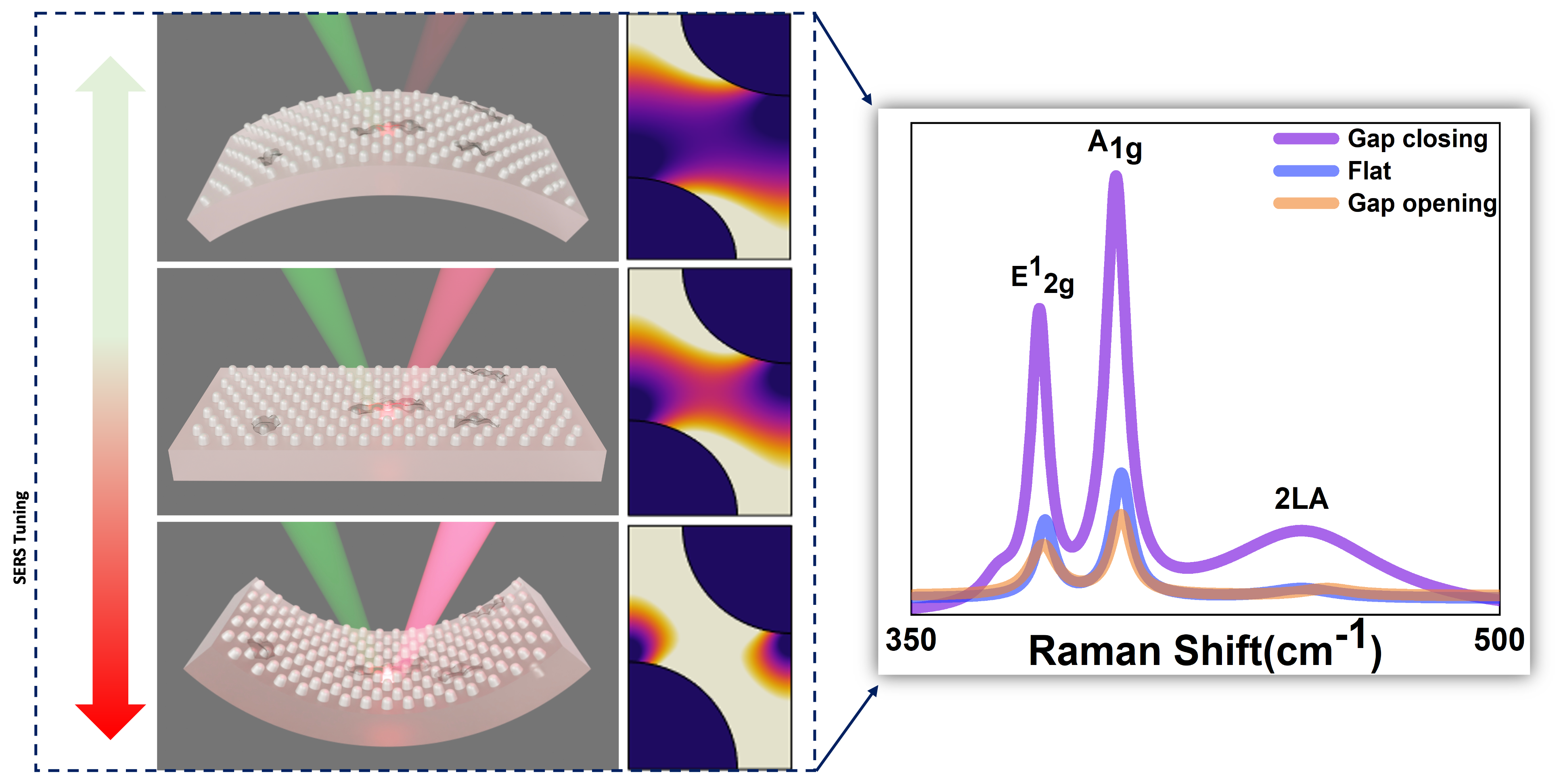
The schematic diagram of the method to tune the SERS intensity of the sample is presented in Figure 3(a). As the sample is on a flexible substrate, we can apply both compressive (inward bent) and tensile (outward bent) strain to change the overall gap width in between nanotips which ultimately increase or decrease the localized field intensity (Figure 3(a)). The strain-controlled field confinement eventually manipulates the SERS intensity of 1L MoS2. To avoid any artifact due to change in experimental condition, we fabricated all the sample at the same time with similar dimension and measured under similar bending condition. Furthermore, laser was focused on the same spot on 1L MoS2 for all the measurements at different bending condition (see SI6). The detailed calculation of bending strain is presented in SI9. The sample was bent systematically with a strain magnitude of 0.82 %,1.22 %, 1.57 % in both inward (negative sign) and outward (positive sign) direction. Figure 3(b) and SI10 present the strain dependent Raman spectra of 1L MoS2/PET and 1L MoS2/nanotip. The extracted peak positions (mode peak), FWHM and intensities are summarized in Figure 3(c).
At flat condition, for 1L MoS2/PET, the peak positions of E12g, A1g and 2LA are 384.27 cm-1, 405.82 cm-1, 451.76 cm-1, respectively. For 1L MoS2/nanotip, the respective peaks positions are shifted to 384.04 cm-1, 403.44 cm-1 and 454.06 cm-1. While we observed a small shift (-0.06 %) in E12g peak position, A1g peak is shifted by -0.58 %. Since the E12g peak is insensitive to the substrate features, small peak shift is due to the additional strain induced by nanotip. A huge change in A1g peak is due to the charge doping from nanotip to 2D material[38,39]. The 2LA peak is red shifted by 0.5%. At flat conditions, both FWHM and SERS intensity of MoS2/nanotip is increased because of enhanced strain and field localization in between nanotips.
The mode peak E12g of 1L MoS2/PET is shifted by +0.3 % and -0.4 % when it is under compressive and tensile strain of 1.57 %, respectively as observed by other researchers[40,41]. When 1L MoS2/nanotip is under compressive strain, E12g is red shifted by 0.4 % which is opposite of what we observed in 1L MoS2/PET. To explain this anomaly, we consider that at flat condition 1L MoS2 is fixed on top of nanotip as a tent without slippage. Under compression the contact area between MoS2 and metal increases. As MoS2 approaches the metal surface it takes the shape of the nanotip, and tensile strain is only exerted on 1L MoS2 at the tip of the metal[25] which explains the anomalous redshift of E12g peak under compressive strain. There is a very small change (-0.02%) in E12g peak due to tensile strain on MoS2/nanotip. The out-of-plane vibration mode (A1g) is shifted by -0.18 % and -0.42 % for compressive and tensile strain of same magnitude (1.57 %) for 1L MoS2/PET, respectively. However, it is shifted by -0.31 % (compressive strain) and 0.02 % (tensile strain) for 1L MoS2/nanotip. When 1L MoS2/nanotip is bent inwardly, 1L MoS2 becomes much closer to Ag nanotip, thereby causing n-type doping of 1L MoS2 as confirmed by the redshift of A1g peak. For 2LA peak, the shift is about ~-1.0 % in both bending directions in 1L MoS2/PET sample. The redshift is due to a change in lattice constant which affects the band structure of the material[42,43]. The charge doping and strain also affects the line width of the spectra. FWHM of these modes are inversely proportional to phonon lifetime. We observe that on PET and nanotip, FWHM of 2LA mode increases(decreases) with compressive(tensile) strain which is in good agreement with previous results[44]. Under compressive strain, A1g and E12g peak broadening is observed due to electron-phonon scattering[45] and tensile strain[46], respectively on nanotip array. On the other hand, there is an increase in phonon lifetime in 1L MoS2/PET substrate, which leads to decrease in FWHM. However, for outward bending, the effect of uniaxial tensile strain is dominant rather than doping, leading to increase in FWHM of both the optical phonons in 1L MoS2/nanotip[47,48].
In terms of SERS performance, the strain-controlled intensity change of Raman modes is also investigated. For 1L MoS2/PET, the intensities of all mode peak are decreased significantly by ~75 % for both directions of bending. This decreasing tendency is not desirable for a highly sensitive tunable SERS platform. On the other hand, for MoS2/nanotip, the intensities of the mode peaks E12g, A1g and 2LA are tuned from -45.6 %, -40 %, -33.3 % to +186.7 %, +216.6 %, +374.3 % by simply applying strain from +1.57 % (tensile) to -1.57 % (compressive). Please note that it is surprising to observe that the tuning range is in increasing order from E12g to 2LA, which needs further study. We performed finite element method (FEM) simulation of structural and electromagnetic field of the nanotip array, shown in Figure 3(d), (e). From the structural simulation, it is found that there is enormous strain localization in between the tips when bending strain is applied, which might cause the inter-tip gap width to increase or decrease. The electromagnetic field simulation confirms the increase or decrease of field confinement when the nanotips are closer or far-away (Figure 3(e)). In pursuit of enhancing the SERS intensity, we deposited ~10 nm diameter Ag nanoparticle on 1L MoS2/nanotip array to fabricate nanoparticle/1L MoS2/nanotip geometry. These nanoparticles decorated on 1L MoS2/nanotip would not only exert additional strain but also enhance the field confinement in the gap created by it. The schematic diagram of the sample is presented in Figure 4(a). Shown in Figure 4(b) is the SEM image of Ag nanoparticle deposited on bare nanotip array on PET. From the image, it is observed that the nanoparticles are decorated homogeneously on the surface of the tip. The strain dependent Raman spectra for nanoparticle/1L MoS2/nanotip sample (SI11) are shown in Figure 4(c), SI2. We applied compressive strain to the sample to enhance the Raman signal. We observed E12g mode split into two peaks at 372.85 cm-1 and 381.66 cm-1, suggesting additional strain due to nanoparticles at flat condition[20]. The extracted parameter corresponding to E12g(M), E12g, A1g and 2LA mode is summarized in Figure 4(d). Similar to 1L MoS2/nanotip, there is minor change in peak position of E12g and A1g. However, E12g(M) and 2LA peak shifted by -0.73 % and +0.6 %, respectively. The FWHM of E12g and 2LA peak is increased whereas it decreased for E12g(M) and A1g. It is interesting to point out that the intensity of SERS signal is greatly enhanced as compared to 1L MoS2/nanotip with inclusion of nanoparticles. The significant enhancement in intensity of Raman peaks is due to stronger field localization between nanoparticle and nanotip separated by 1L MoS2. Beyond -1.57 % of strain, the intensity, peak position and FWHM of all the modes are reverted to their initial values. This might be due to the damage or sliding of MoS2 by excessive strain[25].
Enhancement factor is an important parameter to validate the SERS performance (SI13). The experimental enhancement factor (EFExp) is calculated by:
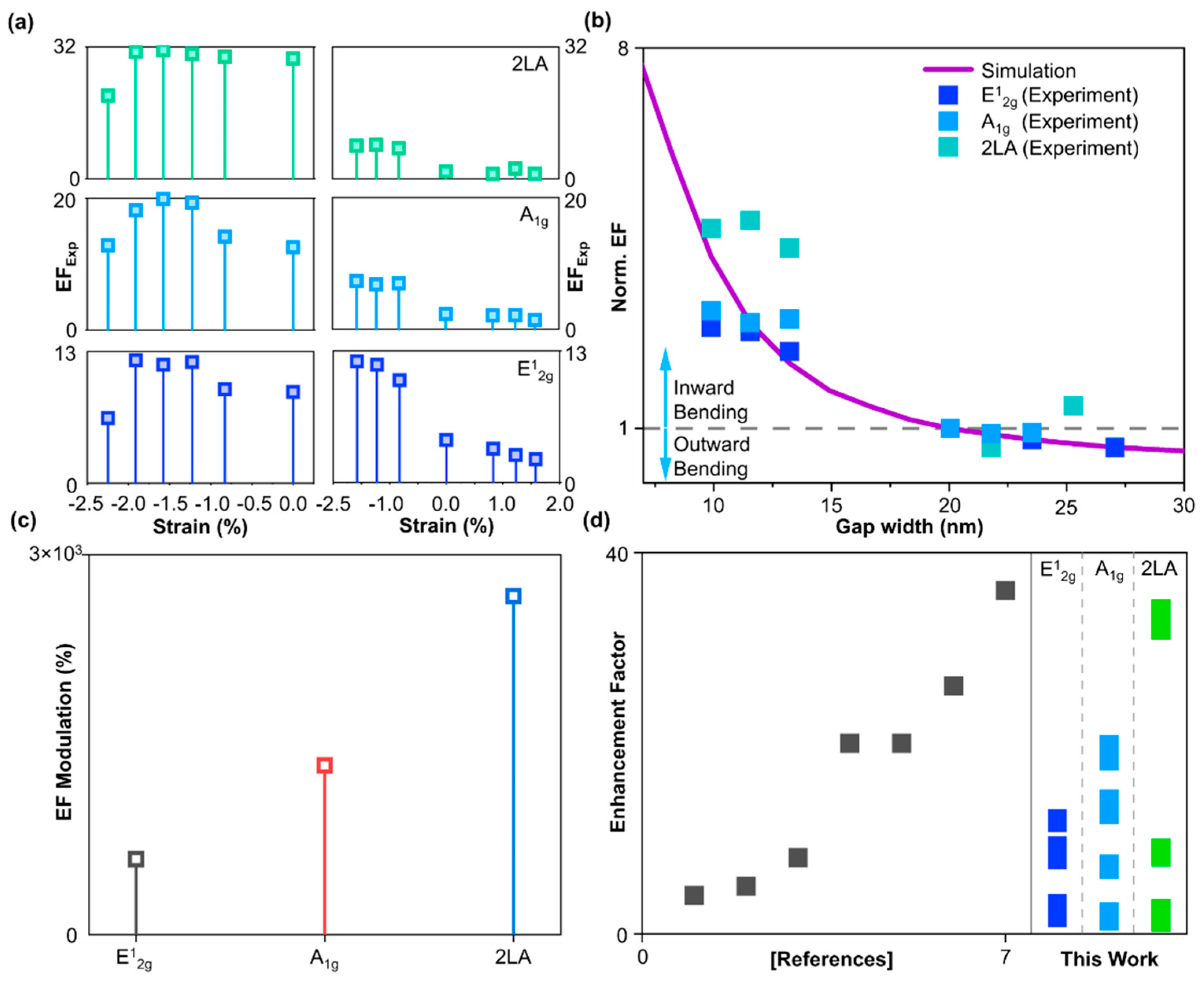
where is the surface enhanced Raman intensity (in our case nanoparticles/1L MoS2/nanotip and 1L MoS2/nanotip), is the Raman intensity of bare 1L MoS2 on PET substrate. The highest enhancement factor is calculated to be 12, 20, 34.1 for E12g, A1g, 2LA mode, respectively, at – 1.57 % (inward) strain for nanoparticles/1L MoS2/nanotip. To find out the strain dependent inter-tip gap width change, the simulated enhancement factor for different gap width is normalized and compared with normalized EFexp, shown in Figure 5(b) (SI14 and SI15). From the data, it is concluded that there is an overall gap width increase (decrease) of 10 nm for inward (outward) bending. The modulation of depth of enhancement factor is of the order 103 as compared to lowest enhancement factor of 1L MoS2/nanotip at outward bending (Figure 5(c)). We could also achieve initial intensity at flat after bending experiment (SI16), showing reconfigurability of the platform. We checked the intensity at various spots in nanoparticles/1L MoS2/nanotip sample (SI17). We observed similar SERS signals from five different spots, suggesting a large area SERS platform. A comparative study between our work and reported work is presented in SI18 and the respective graph is shown in Figure 5(d). Although some of the work reported a good enhancement factor, our work shows the ability to control the enhancement factor from low to high for first and second order Raman signal.
4. Conclusions
In summary, we demonstrated a mechanically active SERS platform based on nanoparticles/1L MoS2/nanotip and 1L MoS2/nanotip fabricated on PET substrate. We recognized three different mode E12g, A1g and 2LA in Raman spectra of MoS2 on bare substrates and nanotip array. The peak position and FWHM are affected by the external strain induced on it. More importantly, the SERS intensity is enhanced (reduced) significantly with inward bending (outward) of 1L MoS2/nanotip sample. To enhance the signal even more, silver nanoparticles are deposited on 1L MoS2/nanotip sample, forming nanoparticles/1L MoS2/nanotip geometry. With the external inward bending, this sample offered enhancement factor as high as 35. The overall enhancement factor is tuned from 1.23 to 35, showing an excellent tunability of the SERS platform. The change in intensity (or enhancement factor) is due to the change in gap width which is confirmed by FEM structural and electromagnetic simulation. Our work may find applications in developing future tunable devices for energy, sensing, and opto-electronics.
Supplementary Materials
The following supporting information can be downloaded at the website of this paper posted on Preprints.org.
Author Contributions
B.D. and D.S.K. conceptualized the experiment. Y.B.K., S.B, B.D. did the experiment together. B.D. and D.L. worked on optical simulation. All authors contributed to the paper.
Funding
This research was funded by National Research Foundation of Korea (NRF-2015R1A3A2031768, NRF-2022M3H4A1A04096465, NRF-2021R1A6A1A10042944).
Institutional Review Board Statement
Not applicable.
Informed Consent Statement
Not applicable.
Data Availability Statement
Not applicable.
Acknowledgments
We would like to thank UNIST Central Research Facilities (UCRF) at Ulsan National Institute of Science of Technology (UNIST) for providing a facility for Raman measurements.
Conflicts of Interest
The authors declare no conflicts of interest.
References
- Langer, J.; de Aberasturi, D.J.; Aizpurua, J.; Alvarez-Puebla, R.A.; Auguié, B.; Baumberg, J.J.; Bazan, G.C.; Bell, S.E.J.; Boisen, A.; Brolo, A.G.; Choo, J.; Cialla-May, D.; Deckert, V.; Fabris, L.; Faulds, K.; de Abajo, F.J.G.; Goodacre, R.; Graham, D.; Haes, A.J.; Haynes, C.L.; Huck, C.; Itoh, T.; Käll, M.; Kneipp, J.; Kotov, N.A.; Kuang, H.; Le Ru, E.C.; Lee, H.K.; Li, J.-F.; Ling, X.Y.; Maier, S.A.; Mayerhöfer, T.; Moskovits, M.; Murakoshi, K.; Nam, J.-M.; Nie, S.; Ozaki, Y.; Pastoriza-Santos, I.; Perez-Juste, J.; Popp, J.; Pucci, A.; Reich, S.; Ren, B.; Schatz, G.C.; Shegai, T.; Schlücker, S.; Tay, L.-L.; Thomas, K.G.; Tian, Z.-Q.; Van Duyne, R.P.; Vo-Dinh, T.; Wang, Y.; Willets, K.A.; Xu, C.; Xu, H.; Xu, Y.; Yamamoto, Y.S.; Zhao, B.; Liz-Marzán, L.M. Present and Future of Surface-Enhanced Raman Scattering. ACS Nano 2020, 14, 28. [Google Scholar] [CrossRef]
- Guselnikova, O.; Lim, H.; Kim, H.-J.; Kim, S.H.; Gorbunova, A.; Eguchi, M.; Postnikov, P.; Nakanishi, T.; Asahi, T.; Na, J.; Yamauchi, Y. New Trends in Nanoarchitectured SERS Substrates: Nanospaces, 2D Materials, and Organic Heterostructures. Small 2022, 18, 2107182. [Google Scholar] [CrossRef] [PubMed]
- Solís, D.M.; Taboada, J.M.; Obelleiro, F.; Liz-Marzán, L.M.; de Abajo, F.J.G. Optimization of Nanoparticle-Based SERS Substrates through Large-Scale Realistic Simulations. ACS Photonics 2017, 4, 329. [Google Scholar] [CrossRef] [PubMed]
- P. L. Stiles, J. A. Dieringer, N. C. Shah, and R. P. Van Duyne, Surface-Enhanced Raman Spectroscopy, Annu. Rev. Anal. Chem 2008, 1, 601. [CrossRef]
- Kim, D.; Ko, Y.; Kwon, G.; Kim, U.-J.; Lee, J.H.; You, J. 2,2,6,6-Tetramethylpiperidine-1-Oxy- Oxidized Cellulose Nanofiber-Based Nanocomposite Papers for Facile In Situ Surface-Enhanced Raman Scattering Detection. ACS Sustain. Chem. Eng. 2019, 7, 15640. [Google Scholar] [CrossRef]
- Yilmaz, M.; Senlik, E.; Biskin, E.; Yavuz, M.S.; Tamer, U.; Demirel, G. Combining 3-D Plasmonic Gold Nanorod Arrays with Colloidal Nanoparticles as a Versatile Concept for Reliable, Sensitive, and Selective Molecular Detection by SERS. Phys. Chem. Chem. Phys. 2014, 16, 5563. [Google Scholar] [CrossRef] [PubMed]
- Park, S.; Lee, J.; Ko, H. Transparent and Flexible Surface-Enhanced Raman Scattering (SERS) Sensors Based on Gold Nanostar Arrays Embedded in Silicon Rubber Film. ACS Appl. Mater. Interfaces 2017, 9, 44088. [Google Scholar] [CrossRef]
- Schwenk, N.; Mizaikoff, B.; Cárdenas, S.; López-Lorente, Á.I. Gold-Nanostar-Based SERS Substrates for Studying Protein Aggregation Processes. Analyst 2018, 143, 5103. [Google Scholar] [CrossRef]
- Qiu, H.; Huo, Y.; Li, Z.; Zhang, C.; Chen, P.; Jiang, S.; Xu, S.; Ma, Y.; Wang, S.; Li, H. Surface- Enhanced Raman Scattering Based on Controllable-Layer Graphene Shells Directly Synthesized on Cu Nanoparticles for Molecular Detection. ChemPhysChem 2015, 16, 2953. [Google Scholar] [CrossRef]
- Zhang, E.; Xing, Z.; Wan, D.; Gao, H.; Han, Y.; Gao, Y.; Hu, H.; Cheng, Z.; Liu, T. Surface-Enhanced Raman Spectroscopy Chips Based on Two-Dimensional Materials beyond Graphene. J. Semicond. 2021, 42, 51001. [Google Scholar] [CrossRef]
- Oliverio, M.; Perotto, S.; Messina, G.C.; Lovato, L.; De Angelis, F. Chemical Functionalization of Plasmonic Surface Biosensors: A Tutorial Review on Issues, Strategies, and Costs. ACS Appl. Mater. Interfaces 2017, 9, 29394. [Google Scholar] [CrossRef]
- Zhang, S.; Geryak, R.; Geldmeier, J.; Kim, S.; Tsukruk, V.V. ; Synthesis; Assembly, and Applications of Hybrid Nanostructures for Biosensing. Chem. Rev. 2017, 117, 12942. [Google Scholar] [CrossRef] [PubMed]
- Kwon, G.; Kim, J.; Kim, D.; Ko, Y.; Yamauchi, Y.; You, J. Nanoporous Cellulose Paper-Based SERS Platform for Multiplex Detection of Hazardous Pesticides. Cellulose 2019, 26, 4935. [Google Scholar] [CrossRef]
- Du, J.; Jing, C. Preparation of Thiol Modified Fe3O4@Ag Magnetic SERS Probe for PAHs Detection and Identification. J. Phys. Chem. C 2011, 115, 17829. [Google Scholar] [CrossRef]
- Raja, S.S.; Cheng, C.-W.; Sang, Y.; Chen, C.-A.; Zhang, X.-Q.; Dubey, A.; Yen, T.-J.; Chang, Y.-M.; Lee, Y.-H.; Gwo, S. Epitaxial Aluminum Surface-Enhanced Raman Spectroscopy Substrates for Large-Scale 2D Material Characterization. ACS Nano 2020, 14, 8838. [Google Scholar] [CrossRef]
- Jin, B.; He, J.; Li, J.; Zhang, Y. Lotus Seedpod Inspired SERS Substrates: A Novel Platform Consisting of 3D Sub-10 Nm Annular Hot Spots for Ultrasensitive SERS Detection. Adv. Opt. Mater. 2018, 6, 1800056. [Google Scholar] [CrossRef]
- Tong, L.; Xu, H.; Käll, M. Nanogaps for SERS Applications. MRS Bull. 2014, 39, 163. [Google Scholar] [CrossRef]
- Luo, W.; Xiong, W.; Han, Y.; Yan, X.; Mai, L. Application of Two-Dimensional Layered Materials in Surface-Enhanced Raman Spectroscopy (SERS). Phys. Chem. Chem. Phys. 2022, 24, 26398. [Google Scholar] [CrossRef]
- Chen, M.; Liu, D.; Du, X.; Lo, K.H.; Wang, S.; Zhou, B.; Pan, H. 2D Materials: Excellent Substrates for Surface-Enhanced Raman Scattering (SERS) in Chemical Sensing and Biosensing. TrAC Trends Anal. Chem. 2020, 130, 115983. [Google Scholar] [CrossRef]
- Moe, Y.A.; Sun, Y.; Ye, H.; Liu, K.; Wang, R. Probing Evolution of Local Strain at MoS2- Metal Boundaries by Surface-Enhanced Raman Scattering. ACS Appl. Mater. Interfaces 2018, 10, 40246. [Google Scholar] [CrossRef]
- Shinde, S.M.; Das, T.; Hoang, A.T.; Sharma, B.K.; Chen, X.; Ahn, J.-H. Surface- Functionalization-Mediated Direct Transfer of Molybdenum Disulfide for Large-Area Flexible Devices. Adv. Funct. Mater. 2018, 28, 1706231. [Google Scholar] [CrossRef]
- Sun, H.; Yao, M.; Liu, S.; Song, Y.; Shen, F.; Dong, J.; Yao, Z.; Zhao, B.; Liu, B. SERS Selective Enhancement on Monolayer MoS2 Enabled by a Pressure-Induced Shift from Resonance to Charge Transfer. ACS Appl. Mater. Interfaces 2021, 13, 26551. [Google Scholar] [CrossRef] [PubMed]
- Lu, D.; Chen, Y.; Kong, L.; Luo, C.; Lu, Z.; Tao, Q.; Song, W.; Ma, L.; Li, Z.; Li, W.; Liu, L.; Li, Q.; Yang, X.; Li, J.; Li, J.; Duan, X.; Liao, L.; Liu, Y. Strain-Plasmonic Coupled Broadband Photodetector Based on Monolayer MoS2. Small 2022, 18, 2107104. [Google Scholar] [CrossRef]
- Xiang, J.; Ali, R.N.; Yang, Y.; Zheng, Z.; Xiang, B.; Cui, X. Monolayer MoS2 Thermoelectric Properties Engineering via Strain Effect. Phys. E Low-Dimensional Syst. Nanostructures 2019, 109, 248. [Google Scholar] [CrossRef]
- Huang, Z.; Lu, N.; Wang, Z.; Xu, S.; Guan, J.; Hu, Y. Large-Scale Ultrafast Strain Engineering of CVD-Grown Two-Dimensional Materials on Strain Self-Limited Deformable Nanostructures toward Enhanced Field-Effect Transistors. Nano Lett. 2022, 22, 7734. [Google Scholar] [CrossRef] [PubMed]
- Wang, H.; Cui, L.; Chen, S.; Guo, M.; Lu, S.; Xiang, Y. A New Perspective on Metal Particles Enhanced MoS2 Photocatalysis in Hydrogen Evolution: Excited Electric Field by Surface Plasmon Resonance. J. Appl. Phys. 2019, 126, 15101. [Google Scholar] [CrossRef]
- Xu, H. Enhanced Light–Matter Interaction of a MoS2 Monolayer with a Gold Mirror Layer. RSC Adv. 2017, 7, 23109. [Google Scholar] [CrossRef]
- Wen, L.; Xu, R.; Mi, Y.; Lei, Y. Multiple Nanostructures Based on Anodized Aluminium Oxide Templates. Nat. Nanotechnol. 2017, 12, 244. [Google Scholar] [CrossRef]
- Robatjazi, H.; Bahauddin, S.M.; Macfarlan, L.H.; Fu, S.; Thomann, I. Ultrathin AAO Membrane as a Generic Template for Sub-100 Nm Nanostructure Fabrication. Chem. Mater. 2016, 28, 4546. [Google Scholar] [CrossRef]
- Tian, G.; Chen, D.; Yao, J.; Luo, Q.; Fan, Z.; Zeng, M.; Zhang, Z.; Dai, J.; Gao, X.; Liu, J.-M. BiFeO3 Nanorings Synthesized via AAO Template-Assisted Pulsed Laser Deposition and Ion Beam Etching. RSC Adv. 2017, 7, 41210. [Google Scholar] [CrossRef]
- M.-L. Tsai, S.-H. Su, J.-K. Chang, D.-S. Tsai, C.-H. Chen, C.-I. Wu, L.-J. Li, L.-J. Chen, and J.-H. He, Monolayer MoS2 Heterojunction Solar Cells, ACS Nano 2014, 8, 8317. [CrossRef]
- Chen, S.; Kim, S.; Chen, W.; Yuan, J.; Bashir, R.; Lou, J.; van der Zande, A.M.; King, W.P. Monolayer MoS2 Nanoribbon Transistors Fabricated by Scanning Probe Lithography. Nano Lett. 2019, 19, 2092. [Google Scholar] [CrossRef]
- Splendiani, A.; Sun, L.; Zhang, Y.; Li, T.; Kim, J.; Chim, C.-Y.; Galli, G.; Wang, F. Emerging Photoluminescence in Monolayer MoS2. Nano Lett. 2010, 10, 1271. [Google Scholar] [CrossRef] [PubMed]
- Lee, C.; Yan, H.; Brus, L.E.; Heinz, T.F.; Hone, J.; Ryu, S. Anomalous Lattice Vibrations of Single- and Few-Layer MoS2. ACS Nano 2010, 4, 2695. [Google Scholar] [CrossRef] [PubMed]
- Conley, H.J.; Wang, B.; Ziegler, J.I.; Haglund, R.F.J.; Pantelides, S.T.; Bolotin, K.I. Bandgap Engineering of Strained Monolayer and Bilayer MoS2. Nano Lett. 2013, 13, 3626. [Google Scholar] [CrossRef] [PubMed]
- Xiao, S.; Xiao, P.; Zhang, X. Atomic-layer soft plasma etching of MoS2. Sci Rep 2016, 6, 19945. [Google Scholar] [CrossRef]
- Carvalho, B.R.; Wang, Y.; Mignuzzi, S.; Roy, D.; Terrones, M.; Fantini, C.; Crespi, V.H.; Malard, L.M.; Pimenta, M.A. Intervalley Scattering by Acoustic Phonons in Two-Dimensional MoS2 Revealed by Double-Resonance Raman Spectroscopy. Nat. Commun. 2017, 8, 14670. [Google Scholar] [CrossRef]
- Lin, J.D.; Han, C.; Wang, F.; Wang, R.; Xiang, D.; Qin, S.; Zhang, X.-A.; Wang, L.; Zhang, H.; Wee, A.T.S.; Chen, W. Electron-Doping-Enhanced Trion Formation in Monolayer Molybdenum Disulfide Functionalized with Cesium Carbonate. ACS Nano 2014, 8, 5323. [Google Scholar] [CrossRef]
- Kiriya, D.; Tosun, M.; Zhao, P.; Kang, J.S.; Javey, A. Air-Stable Surface Charge Transfer Doping of MoS2 by Benzyl Viologen. J. Am. Chem. Soc. 2014, 136, 7853. [Google Scholar] [CrossRef]
- Pak, S.; Lee, J.; Lee, Y.-W.; Jang, A.-R.; Ahn, S.; Ma, K.Y.; Cho, Y.; Hong, J.; Lee, S.; Jeong, H.Y.; Im, H.; Shin, H.S.; Morris, S.M.; Cha, S.; Sohn, J.I.; Kim, J.M. Strain-Mediated Interlayer Coupling Effects on the Excitonic Behaviors in an Epitaxially Grown MoS2/WS2 van Der Waals Heterobilayer. Nano Lett. 2017, 17, 5634. [Google Scholar] [CrossRef]
- Frank, O.; Tsoukleri, G.; Parthenios, J.; Papagelis, K.; Riaz, I.; Jalil, R.; Novoselov, K.S.; Galiotis, C. Compression Behavior of Single-Layer Graphenes. ACS Nano 2010, 4, 3131. [Google Scholar] [CrossRef]
- Dadgar, A.M.; Scullion, D.; Kang, K.; Esposito, D.; Yang, E.H.; Herman, I.P.; Pimenta, M.A.; Santos, E.-J.G.; Pasupathy, A.N. Strain Engineering and Raman Spectroscopy of Monolayer Transition Metal Dichalcogenides. Chem. Mater. 2018, 30, 5148. [Google Scholar] [CrossRef]
- Meng, X.; Pandey, T.; Jeong, J.; Fu, S.; Yang, J.; Chen, K.; Singh, A.; He, F.; Xu, X.; Zhou, J.; Hsieh, W.-P.; Singh, A.K.; Lin, J.-F.; Wang, Y. Thermal Conductivity Enhancement in MoS2 under Extreme Strain. Phys. Rev. Lett. 2019, 122, 155901. [Google Scholar] [CrossRef] [PubMed]
- Chakraborty, B.; Bera, A.; Muthu, D.V.S.; Bhowmick, S.; Waghmare, U.V.; Sood, A.K. Symmetry-Dependent Phonon Renormalization in Monolayer MoS2 Transistor. Phys. Rev. B 2012, 85, 161403. [Google Scholar] [CrossRef]
- Velický, M.; Rodriguez, A.; Bouša, M.; Krayev, A.V.; Vondráček, M.; Honolka, J.; Ahmadi, M.; Donnelly, G.E.; Huang, F.; Abruña, H.D.; Novoselov, K.S.; Frank, O. Strain and Charge Doping Fingerprints of the Strong Interaction between Monolayer MoS2 and Gold. J. Phys. Chem. Lett. 2020, 11, 6112. [Google Scholar] [CrossRef] [PubMed]
- Gołasa, K.; Grzeszczyk, M.; Binder, J.; Bożek, R.; Wysmołek, A.; Babiński, A. The Disorder- Induced Raman Scattering in Au/MoS2 Heterostructures. AIP Adv. 2015, 5, 77120. [Google Scholar] [CrossRef]
- Li, Z.; Lv, Y.; Ren, L.; Li, J.; Kong, L.; Zeng, Y.; Tao, Q.; Wu, R.; Ma, H.; Zhao, B.; Wang, D.; Dang, W.; Chen, K.; Liao, L.; Duan, X.; Duan, X.; Liu, Y. Efficient Strain Modulation of 2D Materials via Polymer Encapsulation. Nat. Commun. 2020, 11, 1151. [Google Scholar] [CrossRef]
- Yu, M.-W.; Ishii, S.; Li, S.; Ku, C.-J.; Chen, S.-Y.; Nagao, T.; Chen, K.-P. Enhancing Raman Spectra by Coupling Plasmons and Excitons for Large Area MoS2 Monolayers. Appl. Surf. Sci. 2022, 605, 154767. [Google Scholar] [CrossRef]
Figure 1.
Flexible nano-tip array. (a) Schematic diagram of fabrication process of flexible nanotip array. SEM images of (b) low and (c) high aspect ratio Ag nanotip array fabricated by direct and angle deposition, respectively (scale bar: 100 nm). (d) Distribution of diameter and inter-tip gap of nanotip array sample.
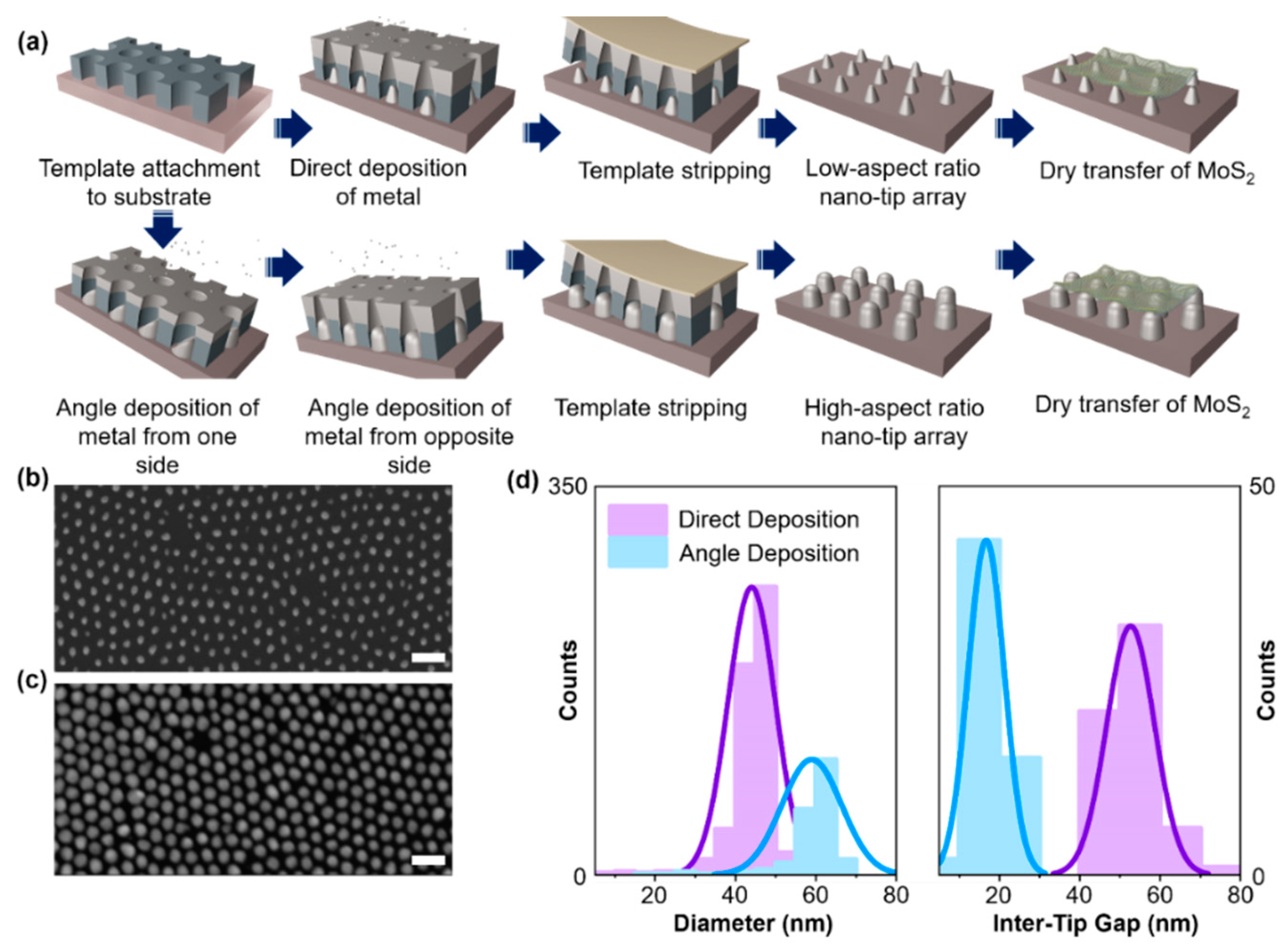
Figure 2.
Surface enhanced Raman scattering of 1L MoS2 enabled by nanotip array. (a) Optical microscope image of monolayer, bilayer(2L) and few-layer MoS2 on nanotip array. Scale bar: 10 um (b) Top view FESEM images of nanotip covered with 1L MoS2. Scale bar: 500 nm. (c) FEM simulation of field confinement in between nanotips of low (left) and high (right) aspect ratio. (d) Raman spectra of 1L MoS2 on PET (left), low aspect ratio (middle), high aspect ratio nanotips (right).
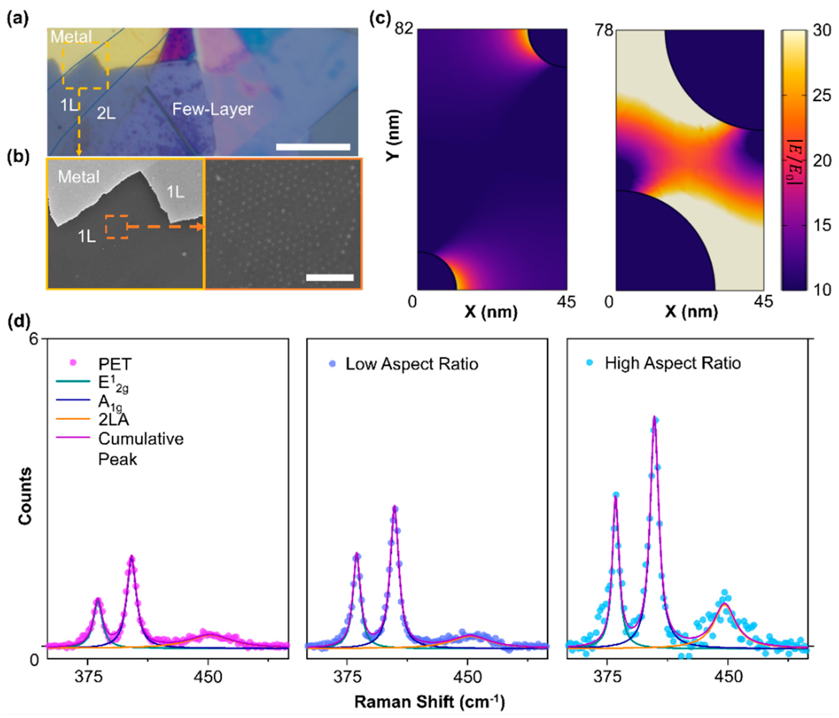
Figure 3.
Tunable SERS platform based on MoS2/Nanotip. (a) Schematic diagram describing tuning methodology of SERS of MoS2/nanotip (top), strain dependent Raman spectra of 1L MoS2/PET (middle) and MoS2/nanotip (bottom). (b) Extracted strain dependent Raman mode peak position, FWHM, intensity of 1L MoS2/PET and 1L MoS2/nanotip. (c) FEM simulation of nanotip array showing stress concentration in between tips under inward bending. (e) Digital images of sample(left) and FEM simulation(right) of field confinement in between tips under inward bent (top), flat (middle), outward bent (bottom) (scale bar: 20 mm).
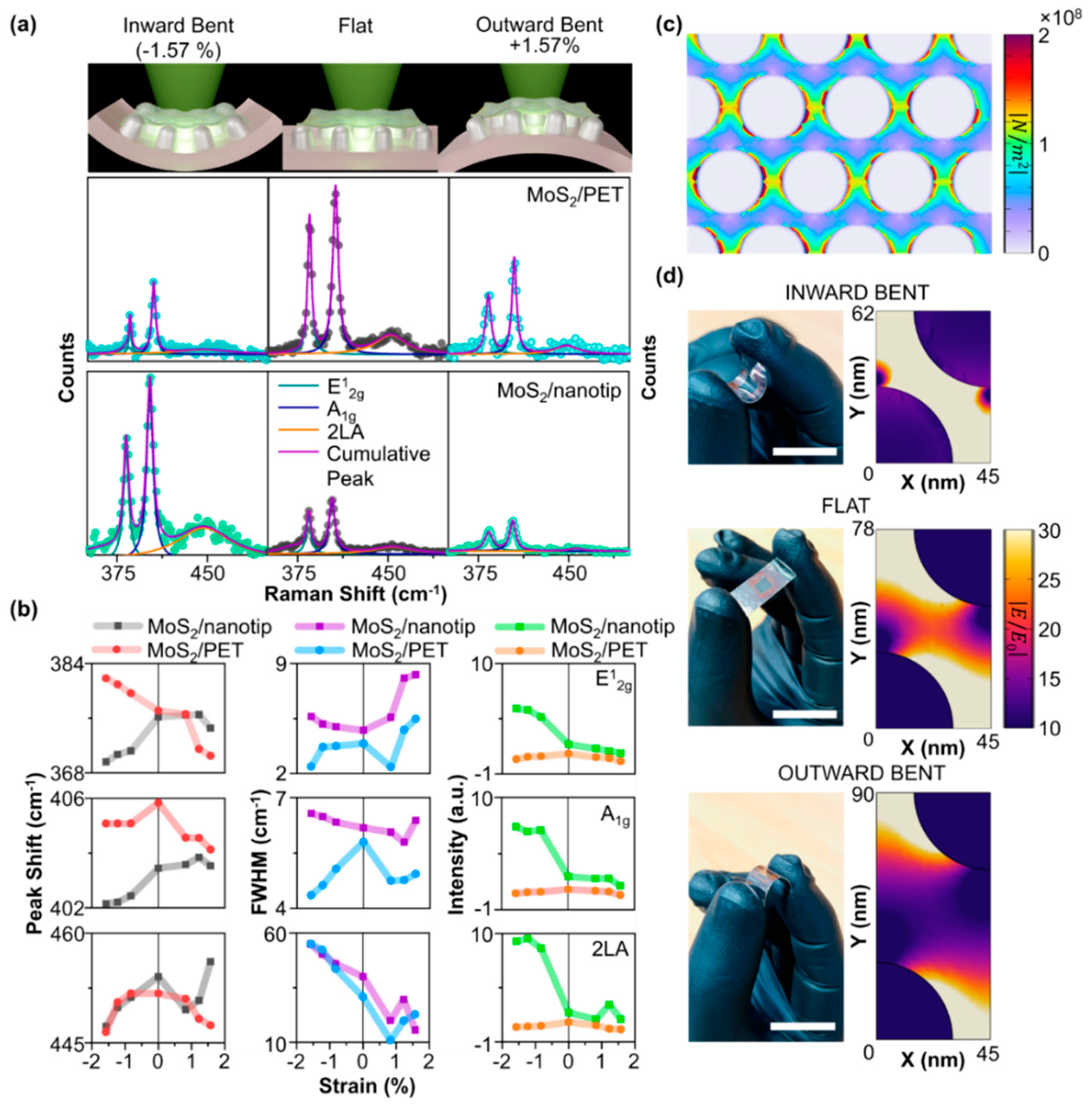
Figure 4.
Tunable SERS platform based on nanoparticles/MoS2/nanotip. (a) Schematic diagram describing tunable SERS platform based on nanoparticles/1L MoS2/nanotip. (b) SEM image of nanoparticle on nanotip sample (scale bar: 100 nm). (c) Compressive strain induced Raman spectra of nanoparticles/1L MoS2/nanotip. (d) Extracted strain dependent Raman mode peak position, FWHM and intensity of nanoparticles/1L MoS2/nanotip.

Figure 5.
Active control of enhancement factor. (a) Strain dependent enhancement factor of nanoparticle/1L MoS2/nanotip and 1L MoS2/nanotip. (b) Depth of modulation of enhancement factor. (c) Finite element simulation of MoS2/nanotip for various inter-dot gap sizes. (d) Literature survey of enhancement factor of 1L MoS2 and comparison with this work.
Disclaimer/Publisher’s Note: The statements, opinions and data contained in all publications are solely those of the individual author(s) and contributor(s) and not of MDPI and/or the editor(s). MDPI and/or the editor(s) disclaim responsibility for any injury to people or property resulting from any ideas, methods, instructions or products referred to in the content. |
© 2024 by the authors. Licensee MDPI, Basel, Switzerland. This article is an open access article distributed under the terms and conditions of the Creative Commons Attribution (CC BY) license (http://creativecommons.org/licenses/by/4.0/).
Copyright: This open access article is published under a Creative Commons CC BY 4.0 license, which permit the free download, distribution, and reuse, provided that the author and preprint are cited in any reuse.


