

Submitted:
08 October 2024
Posted:
10 October 2024
You are already at the latest version
Abstract
This paper presents a comprehensive simulation framework for the investigation of electromigration (EM) in nano-interconnects, with a primary focus on unravelling the influential role of microstructure. To this end, a novel approach to generate conductor metal’s microstructures is presented, whereby a predefined statistical distribution of grain sizes obtained from experimental texture analyses can be incorporated into the developed EM modelling framework. The framework considers the impact of diffusion heterogeneity through the metal texture and interfaces. As such, the intricate interplay between microstructural/interfacial properties, and the resulting atomic flux and stress distribution within nanointerconnects could be investigated. Additionally, the study advances beyond the state of the art by comprehensively simulating all stages of electromigration, including stress evolution, void nucleation, and void dynamics while considering the impact of microstructure. Specifically, the model was employed to study the impact of trench dimensions on dual damascene copper texture and its subsequent impact on electromigration aging, where the model findings were corroborated by comparing to available experimental findings. A nearly linear augmentation in normalized lifetime was detected for aspect ratios equal to or greater than 1. However, a saturation is detected for wider lines with no effective enhancement in lifetime. An aspect ratio of 1 seems to maximize EM lifetime for each cross-sectional area by fostering a bamboo-like structure, where about 2-fold of increase is estimated when going from aspect ratio 2 to 1.
Keywords:
Interconnect
; Electromigration
; Stress evolution
; Void nucleation
; Void-dynamics
; Microstructure
; Grain size
1. Introduction
Electromigration (EM) refers to the phenomenon where the movement of atoms within a conductor is induced by a high-density electric current. This process can lead to the gradual degradation of the conductor, causing, material displacement, void formation and ultimately, device failure. As electronic devices continue to shrink in size and increase in complexity, the current densities in interconnects drastically increase, intensifying the effects of electromigration. This renders the understanding of EM in modern electronics crucial due to its significant implications for device reliability and longevity. Variability of EM time to failure (TTF) has always been a key challenge for back-end-of-line (BEOL) reliability predictions. Experiments have shown that time to failure has a large range of values for similar interconnects fabricated by the same technology and tested under same working conditions. Many factors contribute to TTF variability including the variation in the actual cross-sectional area of the interconnect [1], the variation in quality of the interfaces between the interconnect’s metal and the surrounding materials and other process related factors such as via misalignments. However, one of the most important intrinsic sources of variation is the microstructure of the interconnect. Microstructure has always been identified as a key contributor to the mechanical, thermal, transport and electrical properties of materials [2], and not surprisingly it has been shown to be strongly implicated in EM [3] [4]. Microstructure has been identified to be the main factor causing shortened lifetime of interconnects with down-scaling of the interconnect cross-sectional area for a given current density [3], making the inclusion of microstructure in the modelling of EM in nanointerconnects a very important aspect of a comprehensive and a predictive model.
Numerous scientific contributions have delved into the intricate relationship between microstructural features and the EM behaviour of nanoscale interconnects. Zhang et. al. [4] conducted EM experiments on two sets of Cu-based interconnects with different average grain sizes, that were realized by manipulating the parameters used during electroplating. A 2-fold increase in lifetime was observed for an average grain size of 198 nm compared to a smaller average grain size of 125 nm. A similar work studying the impact of average grain size was done by Choi et. al. [3], where a wider range of variation in average grain size was achieved by varying the trench width while fixing all other fabrication parameters resulting in a significant enhancement in EM lifetime as the metal line width increases from the minimum to three times the minimum width. However, beyond this limit, further widening of the metal line did not yield any additional improvement in EM lifetime. Oates et al. derived the diffusivity coefficients in different diffusion paths (i.e., grain boundaries and interfaces) for estimation of the drift velocity by conducting EM experiments and texture analysis on damascene interconnects fabricated with different dimensions and technological schemes [5].
Only a handful of studies on numerical modelling of EM have attempted to explicitly simulate microstructure by considering heterogeneous diffusivity domains. In contrast, to reduce model complexity and the entailed computational costs, the widely adopted approach has been homogenization using the effective diffusivity concept [6] [7], where a homogenous atomic/vacancy flux through the entire interconnect’s cross-section is employed to approximate the distributed flux through the grain boundaries and interfaces. One of the few such studies was the seminal work by Gleixner [8] where the atomic flux in each type of diffusivity paths was given in terms of the current density and the angle between the path and the vector of the electric current, giving a stress distribution varying between compression and tensile, and concentrated within the diffusivity paths. Later, the impact of microstructure on void dynamics was introduced by Bower [9] where the diffusivity value along the void surface was considered to vary depending on its interaction with grain boundaries and other interfaces causing a variation in the atomic flux. Subsequently, the normal velocity of the void’s surface was estimated using the normal component of the volumetric atomic flux and the divergence of its tangential component. An attempt to include microstructure in both stress evolution and void dynamics was shown separately by Kteyan and Sukharev [10] using the phase field method. An innovative approach to avail of the benefits of the effective model, being its simplicity and low computational cost, while the impact of microstructure could still be approximated, was implemented in the works of Zahedmanesh [11] and Ceric [12], where the interconnect was divided into segments of polycrystalline and single crystal regions, each having its own effective diffusivity value based on the dominating diffusivity path, that is grain boundaries for polycrystalline regions and the cap interface for the single crystals. In essence, the incorporation of microstructure into simulations of EM is indispensable for navigating the challenges posed by the relentless march towards miniaturization in the ever-evolving landscape of nanoelectronics.
The model presented in this investigation constitutes a major enhancement of our antecedent model expounded comprehensively in [7], where detailed expositions and derivations for the pertinent equations and their implementation can be found. Notably, the antecedent model relied upon a singular effective diffusivity coefficient necessitating calibration for each distinct interconnect dimension and technology. In the current study, this aspect has undergone refinement, wherein the solitary effective diffusivity has been supplanted by a more precise distributed diffusivity scheme. The interconnect cross-section is treated as a heterogeneous diffusive medium with distinct paths within a generated microstructure. This approach provides a more nuanced representation of microstructural influences on diffusive processes capturing the impact of dimensional interconnect scaling and technological variations, seamlessly. A visual comparison between the two approaches is shown in Figure 1. The presented model complements existing literature models due to its comprehensive simulation encompassing all stages of EM, including stress evolution, void nucleation, stress relaxation, and void dynamics, along with their intricate interactions with high diffusivity pathways. Additionally, its realistic microstructure generation module considers interconnect aspect ratios, demonstrating commendable alignment with experimental observations.
The subsequent sections of this study are structured as follows; in Section 2, the implemented methodologies are described, encompassing the algorithms employed for the generation of microstructures and the methodology employed for their integration into EM simulations. Subsequently, in section 3, the comprehensive ability of the presented model to capture all stages of EM failure is demonstrated. The simulation framework was then used to study the impact of trench width (and thereby linewidth) on microstructure and EM lifetime, where the simulation was compared with experimental findings. This validation is then followed by an application of the model beyond the experimental domain to reveal the full scaling and aspect ratio impact on EM reliability. Finaly, in section 4, a conclusive summary of the findings is provided.
2. Methods
As a first step, a realistic grain structure has to be implemented. We propose a 2-dimensional model, where grains are spanning the 3rd dimension (i.e., the linewidth). The synthesis of artificial but realistic microstructures for simulation is implemented by employing a novel methodical process. This process is based on the packing of circles of various sizes in the interconnect domain (Figure 2A), where the radii of the circles follow a prescribed statistical distribution, as shown in Figure 2C. This distribution is obtained from experimental grain size analyses on Cu interconnects of different dimensions [13] [3]. The best-fit analysis yielded a lognormal distribution of grain sizes, with an average size approximating the minimum cross-sectional dimension (i.e., the minimum of line width and height) and a standard deviation of ~ 0.45 × average grain size. Initially, the simulation incorporates dynamic packing of the generated circles, which utilizes a random perturbation force and ensures contact resolution amongst the packed circles to minimize their overlap and the inter-circular empty spaces. An example of the dynamic packing process is provided as a video in the supplementary materials. Our algorithm stands out among other algorithms due to its unique feature of ensuring that all circular objects exist as specified from the beginning, thereby preserving the original experimental size distribution. In contrast to other algorithms, such as the random placement [14], which dynamically adds circles based on available spaces left by earlier placements, the utilized approach guarantees the inclusion of all pre-specified circle sizes. This prevents deviation of the size distribution of the circular objects during the packing process from the pre-scribed distribution. Subsequently, circles are used to create actual grains by employing a weighted Voronoi tessellation, also known as the power diagram [15] (Figure 2B). The circles’ centres are utilized as seeds for the Voronoi diagram, while their radii act as weights, influencing the spatial extent of each Voronoi cell to match as closely as possible with the corresponding circle [15]. This weighted Voronoi tessellation creates a microstructure that faithfully represents the specified grain size probability distribution. An example of the described steps to create a microstructure is illustrated in Figure 2.
The microstructure generation module creates the computational domain devised for the resolution of atomic flux, which is a network comprising high-diffusivity paths, specifically the interconnect interface with the cap layer and the grain boundaries. Concomitantly, flux within the bulk and across metal barrier interfaces is disregarded, as substantiated by markedly lower diffusivity values (~10 order of magnitude lower for bulk) [5] [16]. This geometry domain is then used in our finite element (FE) solver, employed within MATLAB®, to model the stress evolution with time. The numerical mesh configuration is accordingly tailored to reflect a higher density at triple points, where the divergence of the atomic flux is most pronounced, and a coarser mesh at the midpoints of the paths, as illustrated in Figure 3. For the calculation of the current density, a separate FE solver is used, following the same principles outlined in our preceding publication [7].
The stress evolution with time is determined by the divergence in atomic flux (i.e., depletion and accumulation of atoms) and is given by [7],
where is the stress, is time, is the bulk modulus, is the atomic volume, is the vacancy relaxation volume, and is the atomic flux. The atomic flux is defined as the summation of the flux driven by the electron wind force and the flux driven by the stress gradient [8],
where is the value of atomic diffusivity in the path where the atomic flux is calculated. For instance, inside grain boundaries and for atomic flux of the cap interface (see Table 1). is the electron wind force, is the Boltzmann constant, and is temperature. The electron wind force on each path is given by the amount of momentum exchange between electrons and atoms in the direction tangential to the path [8],
where is the effective charge, is the electronic charge, is the resistivity, is the current density, and is the angle that the diffusivity path of interest makes with the direction of the electric current flow. In this computational framework, the determination of the atomic flux within each path is initiated by employing equations (2) and (3), with a representative calculation illustrated in Figure 4 for the case of electrons flowing from left to right. At the interconnect boundaries, such as at the end terminals isolated by diffusion barriers, a blocked boundary condition that ensures a zero normal component of the total flux was applied.
The atomic flux takes place along the fast diffusion paths, being higher when the path aligns more closely with the electron flow direction, in contrast to paths perpendicular to it. Subsequently, the flux divergence is computed, elucidating regions where atoms accumulate or deplete, notably at triple points. An illustrative calculation of flux divergence is presented in Figure 5. Finally, the evolution of stress is evaluated for each discrete time step, employing the formulation provided in equation (1). The subsequent phases of the simulation, encompassing void nucleation and void dynamics adhere to the methodologies expounded in our prior publication [7].
For void nucleation, it is imperative to surpass a critical tensile stress threshold, , initiating void growth. Triple points within the microstructure are conducive to nucleation due to their role as focal points for stress evolution and flux divergence. Moreover, the lower activation energy of atoms at triple points reduces the critical stress required for voiding [17]. The stress at the void surface is introduced as a boundary condition post-nucleation. Utilizing the principle of continuity of chemical potential, the stress on the void’s surface, , is related to surface energy, , and curvature, , by equation (4) [7].
Assuming a circular initial void geometry, the initial void radius, , is estimated as outlined in equation (5) [18]. This equation was deduced from minimizing the free energy of a stressed continuum containing a void by variating its size.
The nucleated void generates a new high diffusivity path represented by its free surface. The normal velocity of the evolving void surface under mass transport, , is determined by equation (6) using the calculated flux on the void surface [9].
where is the volumetric flux tangential to the void surface, is the volumetric flux normal to the void surface, and is the void’s surface phase thickness.
3. Results and Discussion
The simulation results on stress evolution, void nucleation, and void dynamics for a 100 long dual damascene Cu interconnect with a linewidth of 40 nm and an aspect ratio (AR) of 2 with a conventional SiCN cap layer, are shown in Figure 6 zoomed on the region of the cathode end for clarity. See Table 1 for the physical parameters and working conditions employed in the simulations.
Because of the substantial difference in stress ranges during the initial phase of stress evolution and subsequent stages of void nucleation and dynamics, distinct color bars are employed to ensure clarity and enhance contrast in stress visualization across all phases. A comprehensive animation illustrating the complete simulation is provided in the supplementary materials, while selected snapshots of interest are highlighted in Figure 6. At the onset (time 0), denoted as the initiation of current flow through the interconnect, a uniform initial stress of 185 MPa is assumed, as estimated in our dedicated thermal-mechanical study [25]. This initial tensile stress originates during the cooling phase from the stress-free temperature down to the working condition temperature, attributed to the differing thermal expansion coefficients of copper (Cu) and the surrounding materials [25]. After current turn-on, momentum exchange between electron wind and the Cu atoms induces an atomic flux through the high-diffusivity paths. Depending on the directions and magnitudes of these fluxes, flux divergence results in either atomic depletion, augmenting the initial tensile stress, or atomic accumulation, shifting the stress towards compression. Large single crystals serve as flux divergence segments, with atomic flux locally occurring solely through the cap interface. In contrast, polycrystalline segments exhibit higher flux due to the presence of both cap interface and grain boundaries as high-diffusivity paths. Subsequently, an increasing number of atoms diffuse toward the anode end, leading to the highest tensile stress near the cathode end, see Figure 6. This stress evolution continues until reaching the minimum critical stress for voiding, assumed to occur at a triple point on the cap interface [26], see Figure 6F. At this juncture, a void nucleates, and tensile stress locally relaxes around the nucleated void [27]. The void undergoes growth primarily under the influence of atomic flux driven by the stress gradient, with regions intersecting high-diffusivity paths expanding more rapidly. As the void continues to grow, the stored mechanical energy is released, leading to stress relaxation and a subsequent weakening of the initially strong gradient, as depicted in Figure 7A, where the onset (time 0) is denoted in this figure as the time of void nucleation. Simultaneously, the reduction of the interconnect’s cross-sectional area due to void growth results in an increase of interconnect resistance (see Figure 7B), generating about 3x increase in current density around the void surface and propelling accelerated void migration toward the cathode end.
Using the developed modelling framework, a comprehensive case study investigating the impact of trench width (and thereby the damascene interconnect’s linewidth) on electromigration was investigated and subsequently compared with experimental data [3] obtained from interconnects with an identical height of 80 nm. Specifically, the experimental trials in [3] involved interconnects with linewidths of 32 nm, 64 nm, 96 nm, and 156 nm. In the simulations, linewidth variations were systematically introduced, ranging from 20 nm to 150 nm. For each simulation data point, a short segment of the generated microstructure at the corresponding scale is exemplified in conjunction with the average grain size (d) in Figure 8.
It is evident that for interconnects with AR<1, the microstructure is predominantly bamboo, and transitions towards increased polycrystallinity and smaller average grain size at narrower linewidths. Thereby, the increased grain boundary density increases the atomic flux and accelerates stress evolution, consequently leading to a reduced time to nucleation. The elongation in time required for nucleation grows proportionally with the expansion of line width, exhibiting a linear trend until reaching an aspect ratio of 0.8, below which it stabilizes. This saturation emerges because, within this range, the constant line height acts as the limiting factor for the average grain size, leading to a saturation point in total diffusivity value and consequently the time needed for nucleation. In Figure 8, the simulation results are compared to experimental findings in [3] demonstrating a correlation that proves the validity of the presented model.
Expanding the scope of this investigation to encompass various line heights provides a comprehensive understanding of the scaling effects on EM lifetime, as depicted in Figure 9. Utilizing simulated data points (see Figure 9 left hand side plot) and using 2D interpolation, the time to nucleation is estimated for each combination of line height and width, extending up to and including 250 nm (see Figure 9 right hand side plot).
The consistent trend of pronounced reliance on linewidth for high aspect ratio lines, followed by a plateauing effect, is evident across all line heights. However, due to the variation in the value of line width at which aspect ratio 1 is reached for each line height, the point of saturation varies accordingly, where doubling the line height for a fixed large line width (i.e., lying in the saturation region) was found to give about 2.5x increase in the value of nucleation time saturation. However, for a fixed small line width (i.e., lying in the aspect ratio 1 and above region) a reduction in time to nucleation is noted as line height increases, even if the minimum cross-sectional dimension dictating the average grain size is the fixed line width. This influence gradually reaches a plateau with further increase in line height. This phenomenon can be attributed to the probability of encountering a single crystal region or a polycrystalline region along the length of the line, quantified by the “p” factor, which is the probability of encountering a polycrystalline region [28] and defined by,
where and are the mean length of the polycrystalline and single crystal regions, respectively. In a single crystal region, the atomic flux relies solely on the cap interface as the primary high diffusivity pathway. Consequently, even with a fixed average grain size dictated by the minimum cross-sectional dimension, elevating the line height diminishes the likelihood of single crystal regions to persist (indicated by a higher “p” factor), until such regions become absent for high aspect ratios (resulting in the “p” factor reaching a maximum of 1). Consequently, subsequent increases in line height exert minimal influence on the time to nucleation. The “p” factor as a function of aspect ratio (AR) is shown in Figure 10, assuming the quality of interfaces is the same across different scales. Results from our simulations in Figure 10, are in perfect agreement with reported experimental studies in [11] for the “p” factor measured at aspect ratios 2 and 3.
In addition to previously discussed cases of varying line height while keeping width constant and vice versa, represented by vertical and horizontal lines on the full scaling colormap (Figure 9, right), there are two additional lines of interest. These include iso-volumetric lines, indicating a fixed cross-sectional area with different aspect ratios (Figure 11, left), and fixed aspect ratio scaling lines, indicating different cross-sectional areas (Figure 11, right). Results indicate that an aspect ratio of 1 maximizes EM lifetime for each cross-sectional area, with an estimated 2-fold increase when moving from an aspect ratio of 2 to 1. This can be explained by the fact that at an aspect ratio of 1, both line width and height are the minimum dimension, allowing microstructure grains to fill the entire interconnect trench cross-section. This fosters a bamboo-like structure, reduces the probability of polycrystalline regions, creates a low diffusivity medium for atomic flux, and extends EM lifetime.
Examining the escalation of resistance post-void nucleation across various dimensions provides insights into the influence of scaling on void growth, as depicted in Figure 11. The figure illustrates three distinct combinations of line height and width. Notably, time 0 is defined as the moment of void nucleation for each case, acknowledging the varying times to nucleation for each case as highlighted earlier.
Comparing the scenario where both line height and width are 80 nm to the case where the line height is 80 nm and the width is 40 nm, illustrates the consequence of altering line width while maintaining a constant line height. Doubling the line width results in approximately a 200-fold increase in the time required to achieve the same rise in resistance. This disparity arises from the heightened presence of grain boundaries interacting with the void surface, attributable to a smaller average grain size in the case of a smaller width. Consequently, a larger flux of atoms migrates away from the void surface, accelerating its growth. Likewise, comparing the scenario where both line height and width are 80 nm to the case where the line height is 160 nm, and the width is 80 nm elucidates the effect of varying line height while keeping line width constant. Doubling the line height leads to approximately a 500-fold increase in the time required to attain the same rise in resistance. This discrepancy is attributed to the larger cross-sectional area, necessitating a greater distance for the void surface to traverse to generate an equivalent resistive impact in the case of a larger height. Finally, comparing the scenario where the line height is 80 nm, and the width is 40 nm with the case where the line height is 160 nm, and the width is 80 nm shows the impact of scaling both dimensions while maintaining a constant aspect ratio. This comparison highlights the most pronounced variation in the time needed for the void to generate the same resistive impact, attributable to the combined influence of a larger average grain size and a larger cross-sectional area.
4. Conclusion
In conclusion, our study presents a comprehensive simulation framework for assessing electromigration failure in nanointerconnects, wherein the nuanced impacts of microstructure, and linewidth scaling, are systematically examined. Our simulation framework captures the entire spectrum of EM stages, including stress evolution, void nucleation, and void dynamics. The modelling of stress evolution unveils the intricate interplay of atomic flux, stress gradients, and microstructural features, shedding light on the dynamics leading to void nucleation. The subsequent void growth phase is characterized by complex interactions, including the release of stored mechanical energy and changes in stress gradients, influencing void growth rates and interconnect resistance. According to our model’s predictions, under the assumption of consistent interface quality across various scales and for the same cross-sectional area, the proportion of polycrystalline segments within the interconnect substantially rises from approximately 10% to around 90% of the total length causing a reduction in lifetime as the aspect ratio escalates from 1 to 2. Notably, for a given cross-sectional area, an aspect ratio of 1 optimizes EM lifetime by minimizing grain boundary density and fostering a bamboo-like structure.
Supplementary Materials
The following supporting information can be downloaded at the website of this paper posted on Preprints.org.
Data Availability Statement
The data that supports the findings of this study are available within the article and its supplementary material.
References
- D.-a. Li and M. Marek-Sadowska, “Variation-aware electromigration analysis of power/ground networks,” in IEEE/ACM International Conference on Computer-Aided Design (ICCAD), 2011.
- H. Clemens, S. Mayer and C. Scheu, Microstructure and Properties of Engineering Materials, Weinheim, Germany: Wiley-VCH Verlag GmbH & Co., 2017.
- S. Choi, C. Christiansen, L. Cao, J. Zhang, R. Flippi, T. Shen, K. B. Yeap, S. Ogden, H. Zhang, B. Fu and P. Justison, “Effect of metal line width on electromigration of BEOL Cu interconnects,” in IEEE (IRPS), Burlingame, CA, 2018.
- L. Zhang, M. Kraatz, O. Aubel, C. Hennesthal, E. Zschech and P. S. Ho, “Grain Size And Cap Layer Effects On Electromigration Reliability Of Cu Interconnects: Experiments And Simulation,” AIP Conference Proceedings, vol. 1300, no. 1, pp. 3-11, 2010.
- A. S. Oates, “Strategies to Ensure Electromigration Reliability of Cu/Low-k Interconnects at 10 nm,” ECS Journal of Solid State Science and Technology, vol. 4, no. 1, p. N3168, 2015.
- M. A. Korhonen, P. Borgesen, K. N. Tu and C.-Y. Li, “Stress evolution due to electromigration in confined metal lines,” Journal of applied physics, vol. 73, no. 8, pp. 3790-3799, 1993.
- A. S. Saleh, K. Croes, H. Ceric, I. De Wolf and H. Zahedmanesh, “A framework for combined simulations of electromigration induced stress evolution, void nucleation, and its dynamics: Application to nano-interconnect reliability,” Journal of Applied Physics, vol. 134, no. 13, p. 135102, 2023.
- R. J. Gleixner and W. D. Nix, “A physically based model of electromigration and stress-induced void formation in microelectronic interconnects,” Journal or applied physics, vol. 86, no. 4, pp. 1932-1944, 1999.
- A. F. Bower and S. Shankar, “A finite element model of electromigration induced void nucleation, growth and evolution in interconnects,” Modell. Simul., pp. 15(8), 923–940, 2007.
- A. Kteyan and V. Sukharev, “Physics-based simulation of stress-induced and electromigration-induced voiding and their interactions in on-chip interconnects,” Microelectronic Engineering, vol. 247, no. 0167-9317, p. 111585, 2021.
- H. Zahedmaesh, O. V. Pedreira, Z. Tokei and K. Croes, “Electromigration limits of copper nano-interconnects,” in IEEE International Reliability Physics Symposium (IRPS), 2021.
- H. Ceric, S. Selberherr, H. Zahedmanesh, R. L. d. Orio and K. Croes, “Review—Modeling Methods for Analysis of Electromigration Degradation in Nano-Interconnects,” ECS Journal of Solid State Science and Technology, vol. 10, no. 3, p. 035003, 2021.
- K. Khoo, S. Tashiro and J. Onuki, “Influence on the Electro-Migration Resistance by Line Width and Average Grain Size along the Longitudinal Direction of Very Narrow Cu Wires,” Materials Transactions, vol. 51, no. 7, pp. 1183-1187, 2010.
- D. He and N. Ekere, “Computer Simulation of Powder Compaction of Spherical Particles,” Journal of Materials Science Letters, vol. 17, no. 20, pp. 1723-1725, 1998.
- Z. Fan, Y. Wu, X. Zhao and Y. Lu, “Simulation of polycrystalline structure with Voronoi diagram in Laguerre geometry based on random closed packing of spheres,” Computational Materials Science, vol. 29, no. 3, pp. 301-308, 2004.
- K. N. Tu, “Recent advances on electromigration in very-large-scale-integration of interconnects,” Journal of Applied Physics, vol. 94, no. 9, pp. 5451-5473, 2003.
- R. J. Gleixner, B. M. Clemens and W. D. Nix, “Void nucleation in passivated interconnect lines: Effects of site geometries, interfaces and interface flaws,” J. Mater. Res., vol. 12, no. 8, pp. 2081-2090, 1997.
- P. A. Flinn, “Mechanical stress in VLSI interconnections: origins, effects, measurements, and modeling,” MRS Bulletin, vol. 20, no. 11, pp. 70-73, 1995.
- H. Zahedmanesh, O. V. Pedreira, C. Wilson, Z. Tőkei and K. Croes, “Copper Electromigration; Prediction of Scaling Limits,” in IEE (IITC), 2019.
- S. P. Hau-Riege and C. V. Thompson, “The effects of the mechanical properties of the confinement material on electromigration in metallic interconnects,” J. Mater. Res., vol. 15, no. 8, pp. 1797-1802, 2000.
- M. McLean, “Determination of the surface energy of copper as a function of crystallographic orientation and temperature,” Acta Metallurgica, vol. 19, no. 4, pp. 387-393, 1971.
- Z. Cui, X. Fan and G. Zhang, “Molecular dynamic study for concentration-dependent volume relaxation of vacancy,” Microelectronics Reliability, vol. 120, no. 0026-2714, pp. 114127,, 2021.
- L. Filipovic, “A method for simulating the influence of grain boundaries and material interfaces on electromigration,” Microelectronics Reliability, vol. 97, no. 0026-2714, pp. 38-52, 2019.
- R. Niu, K. Han, Y.-f. SU, T. Besara, T. M. Siegrist and X. Zuo, “Influence of grain boundary characteristics on thermal stability in nanotwinned copper,” Scientific Reports, vol. 6, no. 1, p. 31410, 2016.
- H. Zahedmanesh, P. R. Besser, C. J. Wilson and K. Croes, “Airgaps in nano-interconnects: Mechanics and impact on electromigration,” Journal of Applied Physics, vol. 120, no. 9, p. 095103, 2016.
- H. Ceric, H. Zahedmanesh and K. Croes, “Analysis of electromigration failure of nano-interconnects through a combination of modeling and experimental methods,” Microelectronics Reliability, Vols. 100-101, p. 113362, 2019.
- F. Yost, D. Amos and A. Romig, “Stress-driven diffusive voiding of aluminum conductor lines,” in 27th Annual Proceedings., International Reliability Physics Symposium, 1989.
- M. L. Dreyer, K. Y. Fu and C. J. Varker, “An electromigration model that includes the effects of microstructure and temperature on mass transport,” Journal of Applied Physics, vol. 73, no. 10, pp. 4894-4902, 1993.
Figure 1.
A comparison between the atomic flux model in (A) the homogenous effective diffusivity approach [7] and (B) the current modelling approach.
Figure 1.
A comparison between the atomic flux model in (A) the homogenous effective diffusivity approach [7] and (B) the current modelling approach.
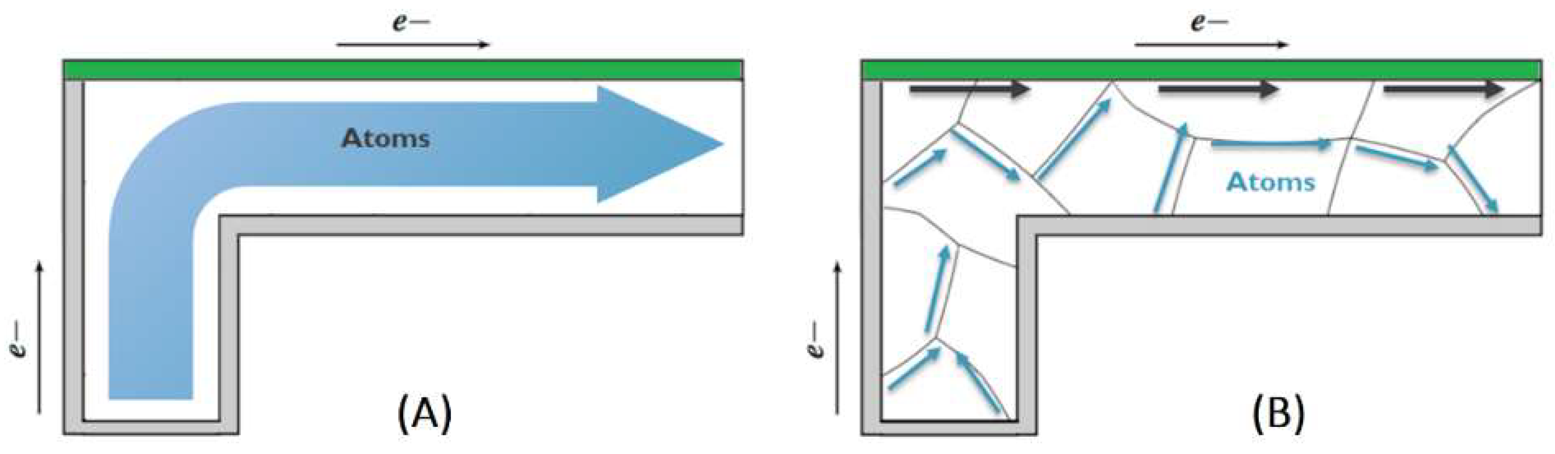
Figure 2.
The model utilised to generate grain microstructures. (A) The packed circles together with their weighted Voronoi tessellation. (B) The created grains from the tessellation after applying grain boundary thickness. (C) The grain size distribution of the generated grains (orange histogram) shown together with the lognormal grain size distribution (continuous black curve).
Figure 2.
The model utilised to generate grain microstructures. (A) The packed circles together with their weighted Voronoi tessellation. (B) The created grains from the tessellation after applying grain boundary thickness. (C) The grain size distribution of the generated grains (orange histogram) shown together with the lognormal grain size distribution (continuous black curve).
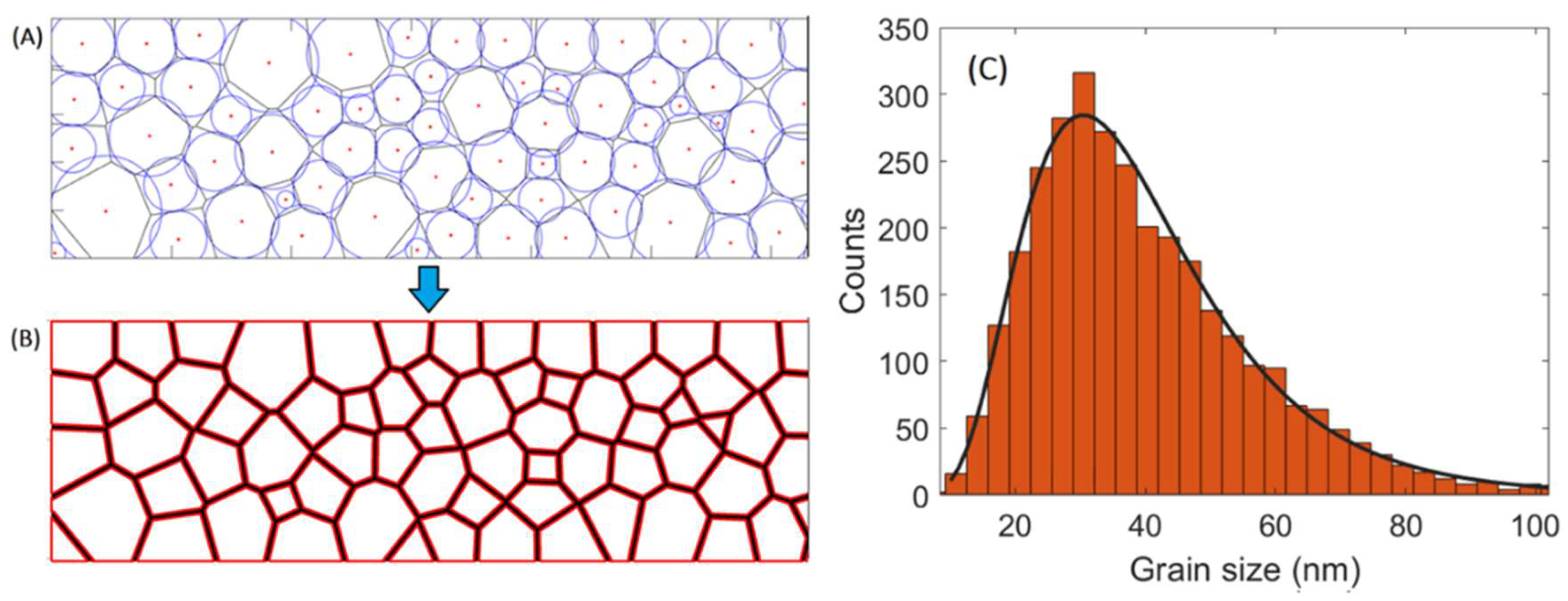
Figure 3.
An example of the meshing scheme applied to our model. Two successive zoom-ins show how the mesh size varies from triple points to the middle of a grain boundary.
Figure 3.
An example of the meshing scheme applied to our model. Two successive zoom-ins show how the mesh size varies from triple points to the middle of a grain boundary.
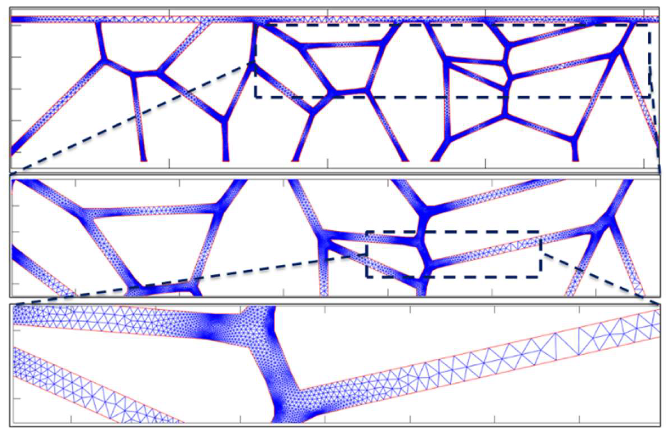
Figure 4.
A vector plot of the atomic flux when electron flow is from left to right. The direction of the blue arrows indicates the atomic flux direction, and their lengths indicate the flux magnitudes.
Figure 4.
A vector plot of the atomic flux when electron flow is from left to right. The direction of the blue arrows indicates the atomic flux direction, and their lengths indicate the flux magnitudes.
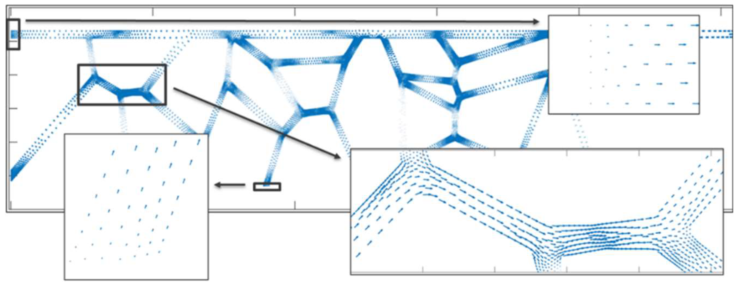
Figure 5.
A colormap indicating the divergence of atomic flux through the diffusion paths’ network. Divergence is non existing along the path and has a positive or negative value at triple points depending on the type and angle of the path.
Figure 5.
A colormap indicating the divergence of atomic flux through the diffusion paths’ network. Divergence is non existing along the path and has a positive or negative value at triple points depending on the type and angle of the path.

Figure 6.
The stress and the void’s geometry change with time shown in a colormap plot. Two color bars are used for clarity, where the top bar has a small range to illustrate the subtle differences in stress along the grain’s boundaries and cap interfaces during the initial stress evolution phase (A-D). The bottom bar has a wide range to illustrate the drastic stress changes pre- and post-void nucleation (E-H). Multimedia is available online.
Figure 6.
The stress and the void’s geometry change with time shown in a colormap plot. Two color bars are used for clarity, where the top bar has a small range to illustrate the subtle differences in stress along the grain’s boundaries and cap interfaces during the initial stress evolution phase (A-D). The bottom bar has a wide range to illustrate the drastic stress changes pre- and post-void nucleation (E-H). Multimedia is available online.
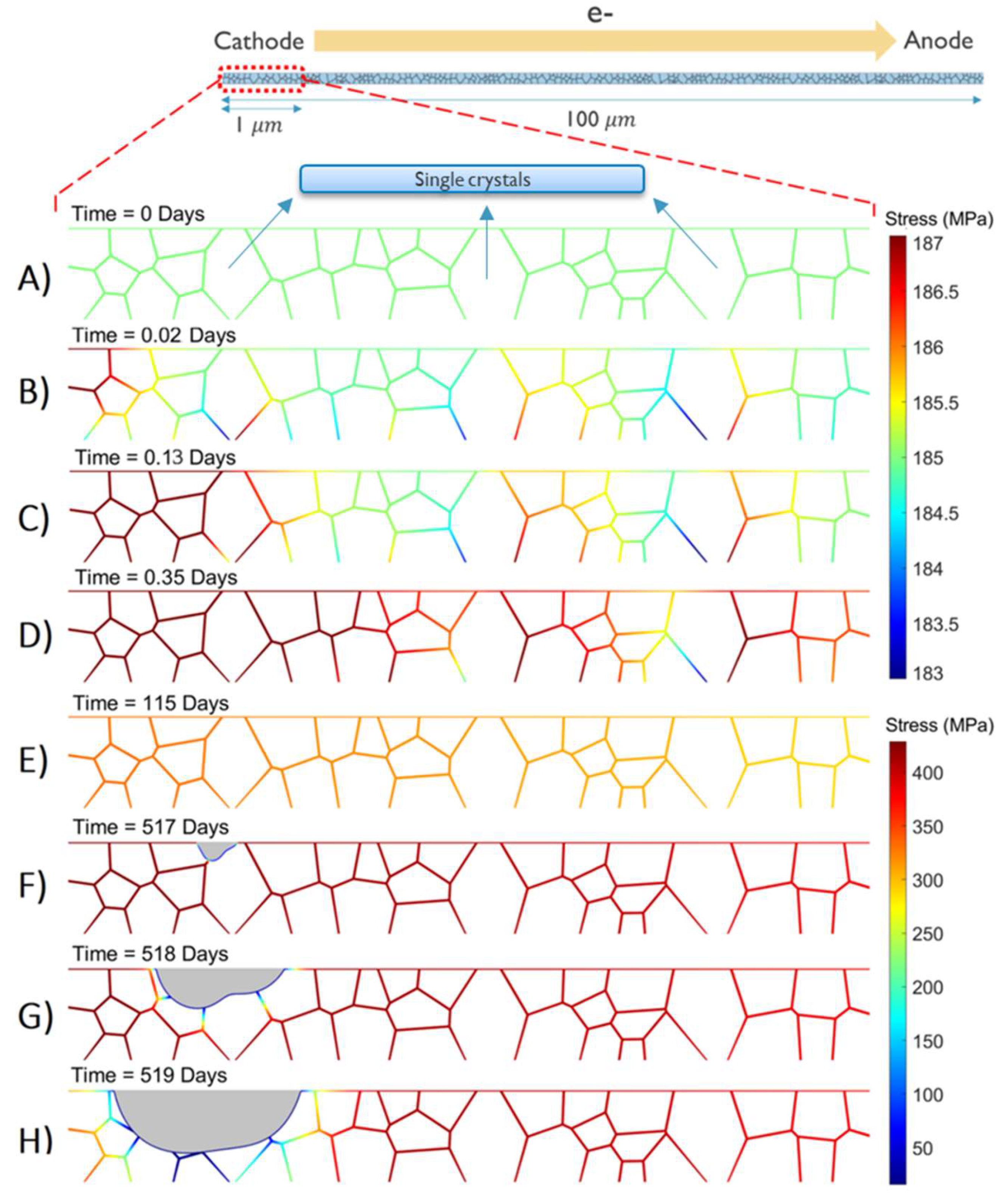
Figure 7.
(A) The stress evolution along the cap interface beyond the void nucleation time. A subplot is showing the stress gradient and the current crowding factor. (B) The simulated electromigration induced increase in resistance with time, showing the three stages of electromigration aging.
Figure 7.
(A) The stress evolution along the cap interface beyond the void nucleation time. A subplot is showing the stress gradient and the current crowding factor. (B) The simulated electromigration induced increase in resistance with time, showing the three stages of electromigration aging.
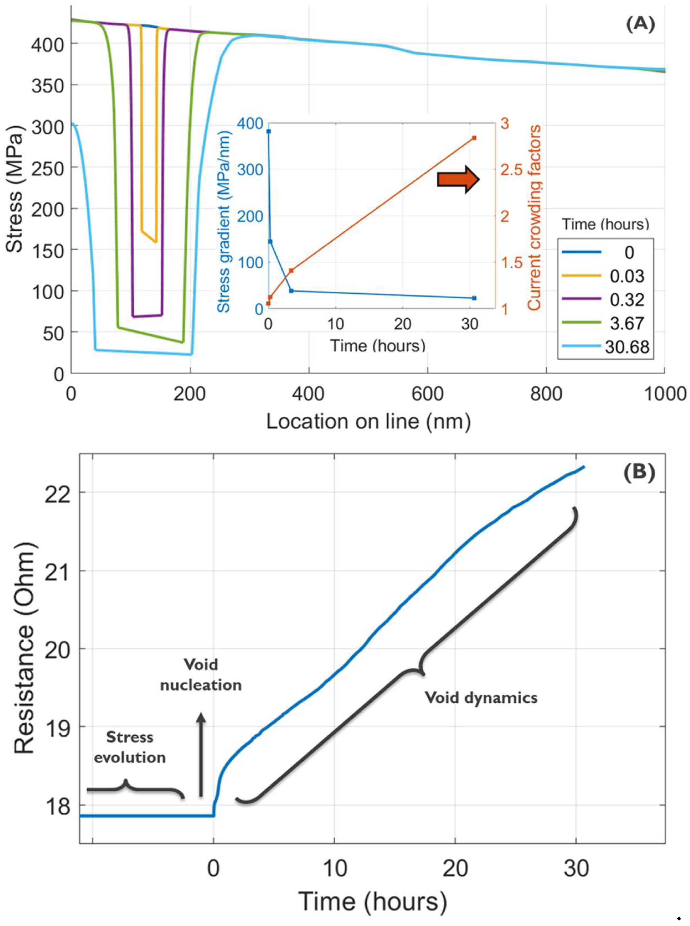
Figure 8.
The time to nucleation normalized to the minimum value for different linewidths as estimated by our model vs. experimental results. For each simulation point, the average grain diameter(d) is shown together with a snapshot of the generated microstructure. Dashed vertical lines mark different aspect ratios.
Figure 8.
The time to nucleation normalized to the minimum value for different linewidths as estimated by our model vs. experimental results. For each simulation point, the average grain diameter(d) is shown together with a snapshot of the generated microstructure. Dashed vertical lines mark different aspect ratios.
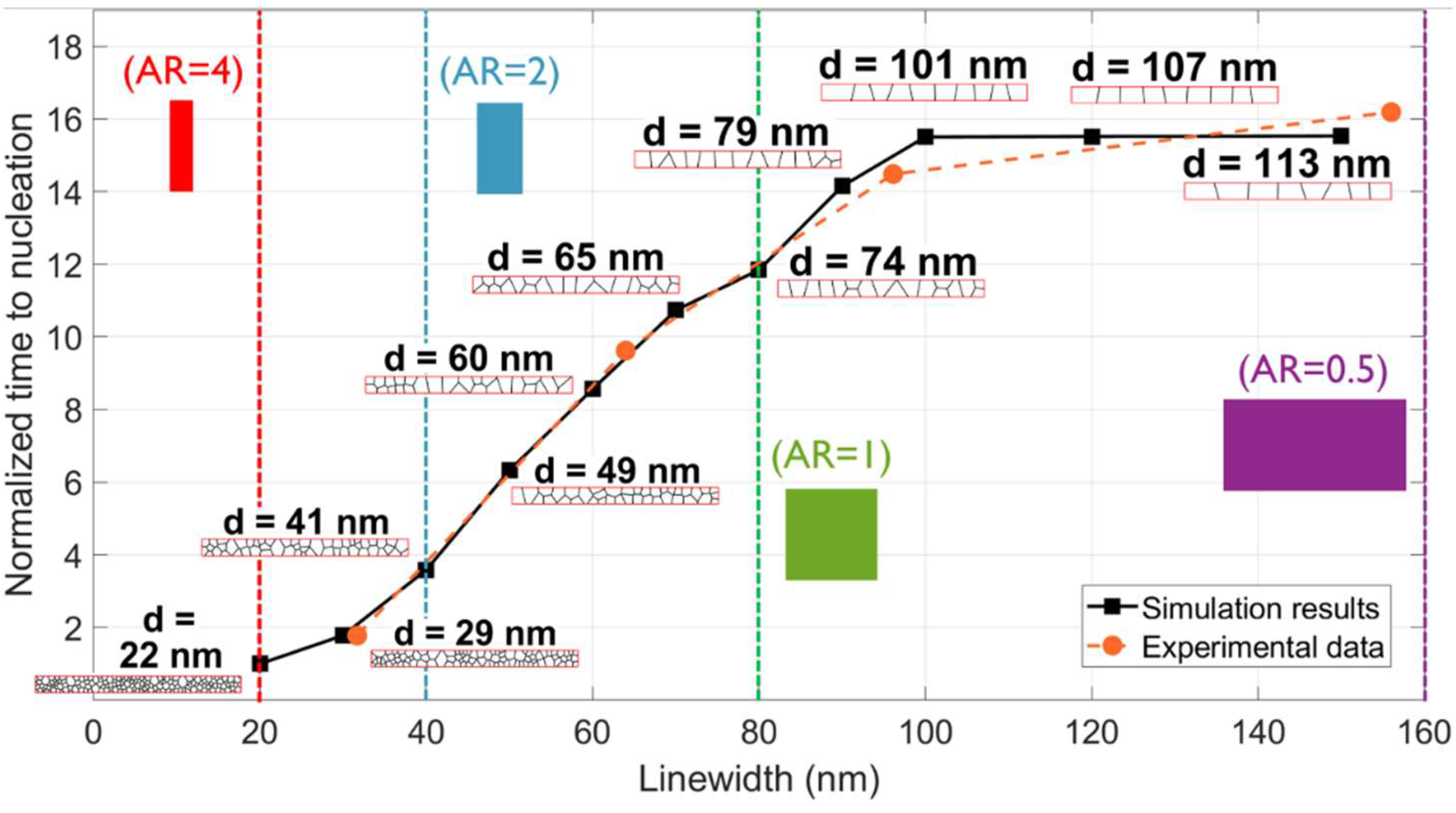
Figure 9.
The full scaling study showing time to nucleation at various linewidth and heights. Values are normalized w.r.t the (80,80) point. All simulation points along with a sigmoid fit (Left). Interpolated surface shown by a colormap (Right).
Figure 9.
The full scaling study showing time to nucleation at various linewidth and heights. Values are normalized w.r.t the (80,80) point. All simulation points along with a sigmoid fit (Left). Interpolated surface shown by a colormap (Right).
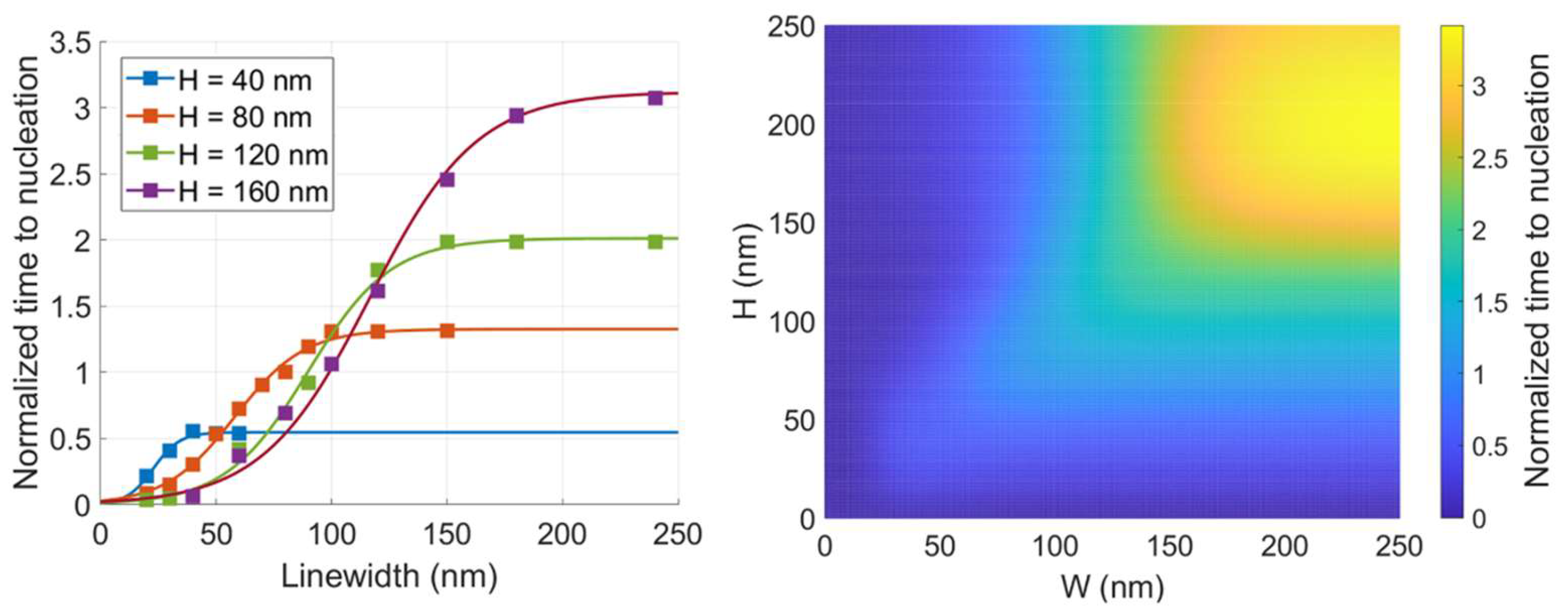
Figure 10.
The “p” factor calculated for different microstructures, generated by our calibrated microstructure module for different aspect ratios (Black points), along with a sigmoid fit to give an analytical formula (Blue line).
Figure 10.
The “p” factor calculated for different microstructures, generated by our calibrated microstructure module for different aspect ratios (Black points), along with a sigmoid fit to give an analytical formula (Blue line).
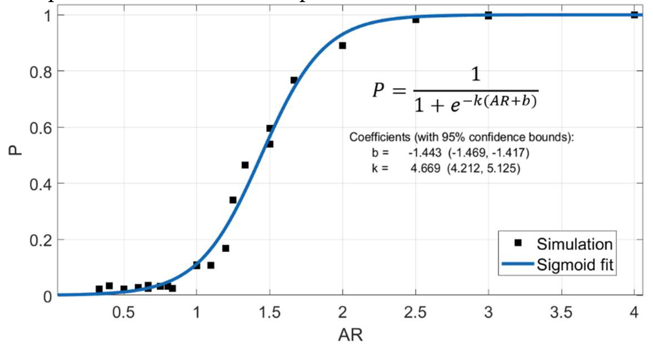
Figure 11.
Time to nucleation (normalized) vs. aspect ratio at different cross-sectional areas (Left). Time to nucleation (normalized) vs. cross-sectional area at different aspect ratios (Right). For each figure, an inset is given to show the lines of interest on the full scaling colormap.
Figure 11.
Time to nucleation (normalized) vs. aspect ratio at different cross-sectional areas (Left). Time to nucleation (normalized) vs. cross-sectional area at different aspect ratios (Right). For each figure, an inset is given to show the lines of interest on the full scaling colormap.
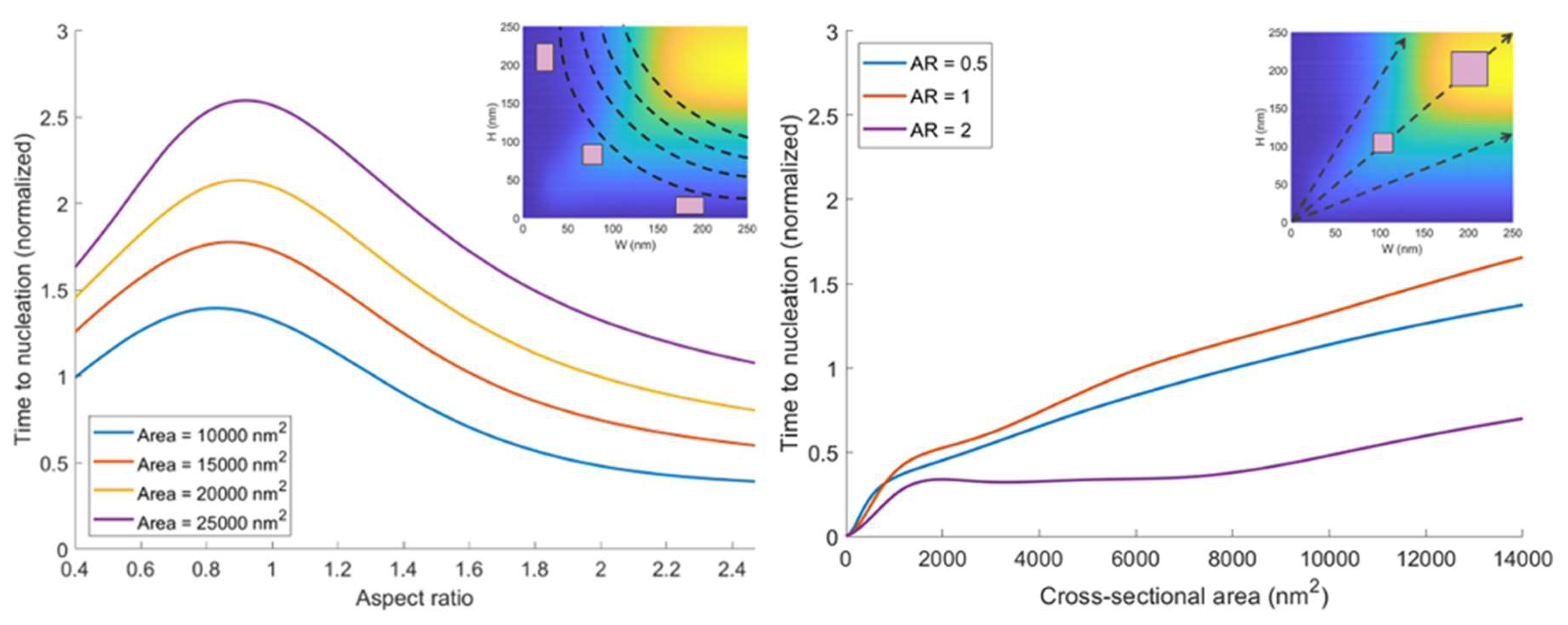
Figure 12.
The EM induced increase in resistance above initial value with time for different cross-sectional dimensions. Time 0 is defined to be the time of void nucleation for each case.
Figure 12.
The EM induced increase in resistance above initial value with time for different cross-sectional dimensions. Time 0 is defined to be the time of void nucleation for each case.
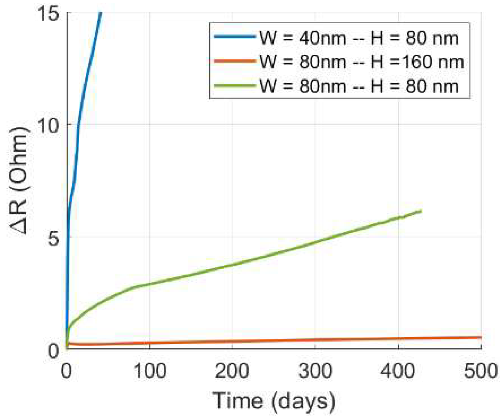

Table 1.
A list of physical input parameters used in the simulations.
| Parameter | Description | Value | Unit | Reference |
|---|---|---|---|---|
| Effective Bulk modulus | 13.3 | GPa | [19] | |
| Poisson ratio | 0.3 | - | [20] | |
| Resistivity | 50 | Ohm.nm | [19] | |
| Surface free energy | 1 | J/m2 | [21] | |
| Effective charge number | 2.38 | - | [19] | |
| Current density | 5 | MA/cm2 | - | |
| Working temperature | 100o | C | - | |
| Vacancy relaxation volume | 0.23 | - | [22] | |
| Initial stress | 185 | MPa | [19] | |
| Critical stress for voiding | 400 - 500 | MPa | [19] | |
| Grain boundary thickness | 1 | nm | [23] [24] | |
| Cap interface thickness | 0.5 | nm | [23] [24] | |
| Grain boundary diffusivity | 0.95 | nm2/s | [5] | |
| Cap interface diffusivity | 0.56 | nm2/s | [5] |
Disclaimer/Publisher’s Note: The statements, opinions and data contained in all publications are solely those of the individual author(s) and contributor(s) and not of MDPI and/or the editor(s). MDPI and/or the editor(s) disclaim responsibility for any injury to people or property resulting from any ideas, methods, instructions or products referred to in the content. |
© 2024 by the authors. Licensee MDPI, Basel, Switzerland. This article is an open access article distributed under the terms and conditions of the Creative Commons Attribution (CC BY) license (http://creativecommons.org/licenses/by/4.0/).
Copyright: This open access article is published under a Creative Commons CC BY 4.0 license, which permit the free download, distribution, and reuse, provided that the author and preprint are cited in any reuse.


