

Submitted:
07 October 2024
Posted:
07 October 2024
You are already at the latest version
Abstract
Current-induced field-free magnetic switching using spin-orbit torque has been an important topic for decades due to both academic and industrial interest. Most research has focused on introducing symmetry breakers, such as geometrical and compositional variation, pinned layer, and symmetry-broken crystal structures, which add complexity to the magnetic structure and fabrication process. We designed relatively simple magnetic structure, composed of a [Co/Pt] multilayer and a Co layer with perpendicular and in-plane magnetic anisotropy, respectively, with a Cu layer between them. Current-induced deterministic magnetic switching was observed in this magnetic system. The system is advantageous for its easy control of the parameters to achieve the optimal condition for magnetic switching. The balance between magnetic anisotropic strength and interlayer coupling strength is found to provide the optimal condition. This simple design and easy adjustability opens various possibilities for magnetic structures in spin-based electronics applications using spin-orbit torque.
Keywords:
spintronics
; spin hall effect
; spin-transfer-torque
; epitaxial film
; magnetic reversal
1. Introduction
Field-free magnetic switching, using spin-orbit torque (SOT), has emerged as a promising technique in spintronics, particularly for applications in magnetic random-access memory (MRAM) [1,2,3], spin logic devices [4,5], and spin oscillators [6,7]. The concept of SOT involves the use of spin currents generated by the spin Hall effect or Rashba-Edelstein effect to manipulate the magnetization of a ferromagnetic layer. This method offers significant advantages over traditional spin-valve type MRAMs, which typically require an external magnetic field for deterministic switching, and over spin-transfer torque (STT) mechanisms [8].
The exploration of SOT began in the early 2000s, with initial studies focusing on heavy metals like platinum (Pt) and tantalum (Ta) due to their strong spin-orbit coupling [9,10,11]. Over the years, researchers have demonstrated the potential of SOT in achieving efficient magnetization switching. A significant milestone was the realization of field-free switching by engineering the symmetry of the magnetic heterostructures, such as using canted deposition of materials like molybdenum (Mo) and tungsten (W) [12,13,14].
One of the primary advantages of SOT-based switching is the elimination of the need for an external magnetic field, which simplifies device architecture and reduces power consumption [15,16,17]. Additionally, SOT offers faster switching speeds and higher endurance compared to STT, making it suitable for high-performance memory applications [8]. The ability to achieve deterministic switching through structural engineering, rather than relying solely on material properties, opens new avenues for device optimization.
Despite its advantages, SOT-based switching faces several challenges. The efficiency of spin current generation and transfer is highly dependent on the materials and their interfaces, which can complicate the fabrication process. Moreover, symmetry breaking is necessary to achieve uniform and reliable switching across magnetic layer with perpendicular magnetic anisotropy. Researchers have explored the diverse approaches, such as synthetic antiferromagnetic systems [18], magnetic runnel junction with 2D materials [19], in-plane exchange bias [20], and compositional variations in magnetic layer [21], etc. The need for precise control over the growth and deposition of materials adds the complexity and cost to manufacturing SOT-electronic devices .
The Co/Pt multilayer system exhibits several interesting magnetic properties, making it a subject of extensive research in the field of spintronics and magnetic storage technologies. Co/Pt multilayers are known for their strong perpendicular magnetic anisotropy, which means the magnetic moments prefer to align perpendicular to the plane of the layers. [27] This property is crucial for high-density magnetic storage applications. The magnetization and coercivity of Co/Pt multilayers can be tuned by varying the thickness of the Co and Pt layers. Thicker Co layers tend to increase the in-plane magnetic anisotropy, while thinner layers enhance the perpendicular anisotropy. The coercivity, which is the resistance to demagnetization, can also be significantly high, especially when the layers are grown at elevated temperatures. [28] The coupling between Co and Pt layers can lead to complex magnetic behaviors. For instance, the presence of Pt can mediate ferromagnetic coupling between Co layers and its coupling strength and direction of spin alignment shows oscillatory change, depending on nonmagnetic spacer thickness. It is described by the Ruderman-Kittel-Kasuya-Yosida (RKKY) theory [29,30,31,32]. These properties make Co/Pt multilayers a versatile and valuable system for both fundamental research and practical applications in magnetic storage and spintronic devices. In this work, we demonstrate field-free SOT magnetic switching in a [Co/Pt]/Cu/Co system. By optimizing the thicknesses of the Cu and Pt layers to adjust the interlayer exchange coupling and magnetic anisotropy strength, respectively, we achieved the optimal conditions for reliable switching.
2. Experimental Details
Figure 1(a) and (b) illustrate the schematic structure for Hall measurement and the layer stack sequence, respectively. The hall bar consists of two sections: one with dimensions of for current flow, and another with dimensions of for Hall voltage measurement.
The magnetic layer stack sequence is Ta(3)/Pt(4)//Cu()/Co(2), where the numbers in parentheses represent the thickness of each layer in nanometers. Here, and denote the variable thicknesses of the Pt and Cu layers, respectively, and is the number of Co/Pt layers. The nominal thickness of layers was determined by sputtering time with a controlled target growth rate. The Ta layer serves as a buffer at the bottom. The thick Pt layer above the Ta buffer acts as a heavy metal to generate the spin Hall effect. The Cu layer, instead of Pt (or Ru), is used as an interface spacer because it reduces the out-of-plane anisotropy of a single Co(2) layer and has almost no spin Hall angle, meaning it has negligible SOT effect on the Co layer [33,34].
A magnetron sputtering system with an initial base pressure of is used to fabricate samples without breaking the vacuum throughout the entire deposition process. To prevent structural asymmetry due to possible oblique-deposition, we rotated the sample holder during the deposition. For Hall effect measurement, we used a Keithly 6221 current source and Keithly 2182A nanovoltmeter. Magnetic measurements were conducted using Lakeshore VSM model 7400 series.
3. Results And Discussion
Figure 2 shows the magnetic hysteresis loops of magnetic stacks with , and , 3, and 4. The multilayers with and 4 exhibit only in-plane magnetic anisotropy (IMA) (Figure 2(a)), and out-of-plane magnetic anisotropy (OMA) (Figure 2(c)), respectively. In contrast, the multilayer with displays both IMA and OMA (Figure 2(b)). Since the multilayer and the Co layer inherently possess OMA and IMA, respectively, the data in Figure 2 suggests strong interlayer coupling between them, specifically through exchange interaction via the Cu space layer. For , this interlayer coupling causes the perpendicular magnetic moments to rotate in-plane. Conversely, for , the coupling induces the in-plane magnetic moments of the Co layer to rotate perpendicular to the plane. For, the IMA in the Co layer and the OMA in the Co/Pt layer compete to maintain their respective magnetic anisotropies. Given the strong interlayer coupling, it is inferred that the magnetic anisotropy strength on both sides is significantly reduced. The coercive field for IMA in Figure 2(b) is smaller than that in Figure 2(a) , and the coercive field for OMA in Figure 2(b) is smaller than that in Figure 2(c) . The variations in the coercive field are consistent with the scenario of reduced magnetic anisotropy strength.
Figure 3(a) shows the Hall resistance as a function of current for the sample with , and under various fields of 0, 100, and 400 Oe. The current pulse with a duration of 1 ms is applied along the + y-axis to the Hall bar structure depicted in Figure 1(a). The Hall resistance difference is defined as , where and are the resistances when current flows along the positive and negative y-axis, respectively. Because the Hall resistance is due to the anomalous Hall effect induced by the magnetization in the Co/Pt multilayer, the difference indicates magnetic moment polarity switching induced by the combination of applied current and field. For , is observed to be , indicating that the magnetic polarity of the Co/Ft multilayer is deterministically switched solely by the applied current. When , increases to , suggesting that the field enhances the magnetic switching. No further enhancement was observed with an increase in the applied field, i.e., . The switching ratio is defined as to be .
The same measurements were performed for the samples with , and and 4. For , no magnetic polarity change was observed. For , magnetic polarity change was observed only when a magnetic field was applied, indicating no zero field switching. In this case, the externally applied field acts as a symmetry breaker for current-induced magnetic switching. Therefore, the magnetic structure with , and has appropriate interlayer coupling between the Co/Pt multilayer and the Co layer, providing an effective internal field as a symmetry breaker, making current- induced magnetic switching possible.
Figure 3(b) shows the Hall resistance with the filed along the – y-axis. Compared to the data in Figure 3(a), there is almost no change in behaviors with the fields of 0, –100, and – 400 Oe. This indicates that the sample in this study is free from field-dependent directional symmetries, such as geometrical gradient, compositional inhomogeneity and interface DMI effect, for current-induced magnetic switching, other than the internal field due to interlayer coupling. The internal field is found to be biaxial along the y-axis.
To investigate the effects of Cu space layer thickness on magnetic polarity, samples with , , and and 0.9 were fabricated. Their magnetizations were plotted as a function of the field in Figure 4(a) and Figure 4(b), respectively. For , the sample loses its OMA characteristics in the Co/Pt multilayer, and no magnetic polarity switching was observed, as expected. For , both IMA in the Co layer and OMA in the Co/Pt multilayer are maintained. Hall bar measurement was performed and plotted in Figure 4(c). Field-free switching was observed with a value of , which is much smaller than that in Figure 3. The values reach to their maximum at and Oe. The switching ratio is . It can be noted that a decrease in Cu layer thickness enhances interlayer coupling, destroying OMA in the Co/Pt multilayer, and that an increase weakens interlayer coupling, reducing the internal field for current-induced switching, and maintaining the coercive field almost unchanged.
Given the significant dependence of OMA characteristics on Pt thickness in Co/Pt multilayers, samples with , , and and 1.0 were fabricated. Their magnetization was plotted as a function of the field in Figure 5(a) and Figure 5(b), respectively. For , the sample loses its OMA characteristics in the Co/Pt multilayer. Assuming that interlayer coupling through the Cu space layer () is the same as in Figure 2, the loss of OMA is likely due to the reduction of OMA strength with a smaller Pt layer thickness. The reduction is consistent with the results in reference [31]. For , both IMA in the Co layer and OMA in the Co/Pt multilayer are maintained. The coercive field in OMA magnetization significantly increases compared to that in Figure 2(b), indicating enhanced magnetic anisotropy strength. Hall bar measurements were performed and plotted in Figure 5(c). Field-free switching is observed with a value of , which is much smaller than that in Figure 3 and comparable to that in Figure 4. values reach to their maximum at and Oe. The switching ration is found to be . The condition of the internal field from and OMA strength from is not optimal for yielding magnetic switching as effectively as in Figure 3(b).
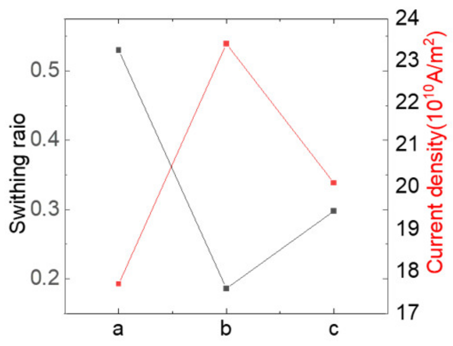
The zero-field switching ratios in Figure 3, Figure 4, and Figure 5, along with the critical current density for switching, are summarized in Figure 6 for comparison.
The sample with , and shows the highest switching ratio () and the lowest critical current density (). In contrast, the sample with , and exhibits the lowest switching ratio () and the highest critical current density (). The sample with , and has a switching ratio of and a critical current density of . Additionally, deviating from the optimal values for both anisotropy and interlayer coupling reduces the effectiveness of magnetic switching, with magnetic anisotropy having a more detrimental effect than interlayer coupling.
4. Conclusions
We report uniform and reliable current-induced field-free switching in a magnetic multilayer system composed of. The magnetic anisotropy strength of the Co/Pt layer can be controlled by varying the number of repetitions and the pt layer thickness . Additionally, the interlayer coupling strength between the Co/Pt and Co layers can be adjusted by changing the Cu layer thickness . Field-free reliable magnetic switching was achieved with the parameter values , and , which provide the optimal conditions for magnetic switching by balancing magnetic anisotropy and interlayer coupling strength. Although other samples with , and , and , and exhibit field-free switching, it is not as effective as the optimal condition.
Using a Co/Pt multilayer with perpendicular magnetic anisotropy and a Co layer for interlayer coupling via a Cu spacer layer exhibited interesting features for field-free magnetic switching: simple structural design, uniform deposition in the fabrication process, biaxial symmetry breaking, and optimization by adjusting appropriate parameters. Our results open possibilities for various designs in SOT-based electronics.
Acknowledgments
This work was supported by a National Research Foundation of Korea (NRF) (No. NRF-2022R1A2C1009516 and RS-2023-00220471) and by the Korea Institute of Industrial Technology (KITECH EH-24-0003)
References
- I.M. Miron et al., Nature 476, 189 (2011).
- A. Brataas, A. D. Kent, and H. Ohno, Nature materials 11, 372 (2012).
- A.D. Kent and D. C. Worledge, Nature nanotechnology 10, 187 (2015).
- S. Manipatruni et al., Nature 565, 35 (2019).
- Z. Luo et al., Nature 579, 214 (2020).
- V. E. Demidov, S. Urazhdin, H. Ulrichs, V. Tiberkevich, A. Slavin, D. Baither, G. Schmitz, and S. O. Demokritov, Nat Mater 11, 1028 (2012).
- M. Haidar, A. A. Awad, M. Dvornik, R. Khymyn, A. Houshang, and J. Akerman, Nat Commun 10, 2362 (2019).
- V. Krizakova, M. Perumkunnil, S. Couet, P. Gambardella, and K. Garello, Journal of Magnetism and Magnetic Materials 562, 169692 (2022).
- L. Zhu, D. C. Ralph, and R. A. Buhrman, Physical Review Applied 10 (2018).
- C. Hong, L. Jin, H. Zhang, M. Li, Y. Rao, B. Ma, J. Li, Z. Zhong, and Q. Yang, Advanced Electronic Materials 4 (2018).
- L. Liu, T. Moriyama, D. C. Ralph, and R. A. Buhrman, Phys Rev Lett 106, 036601 (2011).
- T.-Y. Chen, H.-I. Chan, W.-B. Liao, and C.-F. Pai, Physical Review Applied 10, 044038 (2018).
- K. K. Vudya Sethu, S. Ghosh, S. Couet, J. Swerts, B. Sorée, J. De Boeck, G. S. Kar, and K. Garello, Physical Review Applied 16, 064009 (2021).
- G. Yu et al., Nature nanotechnology 9, 548 (2014).
- K. J. Kim et al., Nat Mater 16, 1187 (2017).
- S. A. Siddiqui, J. Han, J. T. Finley, C. A. Ross, and L. Liu, Phys Rev Lett 121, 057701 (2018).
- K. Cai et al., Nature Electronics 3, 37 (2020).
- A. Fernández-Pacheco, E. Vedmedenko, F. Ummelen, R. Mansell, D. Petit, and R. P. Cowburn, Nature materials 18, 679 (2019).
- E. C. Ahn, npj 2D Materials and Applications 4, 17 (2020).
- A. van den Brink, G. Vermijs, A. Solignac, J. Koo, J. T. Kohlhepp, H. J. M. Swagten, and B. Koopmans, Nat Commun 7, 10854 (2016).
- Z. Zheng et al., Nature communications 12, 4555 (2021).
- A. van den Brink, G. Vermijs, A. Solignac, J. Koo, J. T. Kohlhepp, H. J. Swagten, and B. Koopmans, Nature communications 7, 10854 (2016).
- S. A. Razavi et al., Physical Review Applied 7, 024023 (2017).
- Y.-C. Lau, D. Betto, K. Rode, J. Coey, and P. Stamenov, Nature nanotechnology 11, 758 (2016).
- N. Murray, W.-B. Liao, T.-C. Wang, L.-J. Chang, L.-Z. Tsai, T.-Y. Tsai, S.-F. Lee, and C.-F. Pai, Physical Review B 100, 104441 (2019).
- S. Łazarski, W. Skowroński, J. Kanak, Ł. Karwacki, S. Ziętek, K. Grochot, T. Stobiecki, and F. Stobiecki, Physical Review Applied 12, 014006 (2019).
- C.-J. Lin, G. Gorman, C. Lee, R. Farrow, E. Marinero, H. Do, H. Notarys, and C. Chien, Journal of Magnetism and Magnetic Materials 93, 194 (1991).
- T. Suzuki, H. Notarys, D. C. Dobbertin, C.-J. Lin, D. Weller, D. C. Miller, and G. Gorman, IEEE transactions on magnetics 28, 2754 (1992).
- P. Grünberg, R. Schreiber, Y. Pang, M. Brodsky, and H. Sowers, Physical review letters 57, 2442 (1986).
- R. Duine, K.-J. Lee, S. S. Parkin, and M. D. Stiles, Nature physics 14, 217 (2018).
- S. Parkin, R. Bhadra, and K. Roche, Physical Review Letters 66, 2152 (1991).
- S. S. Parkin, Physical Review Letters 67, 3598 (1991).
- R. Hammerling, C. Uiberacker, J. Zabloudil, P. Weinberger, L. Szunyogh, and J. Kirschner, Physical Review B 66, 052402 (2002).
- M. Gradhand, D. V. Fedorov, P. Zahn, and I. Mertig, Physical Review B—Condensed Matter and Materials Physics 81, 245109 (2010).
Figure 1.
Schematic sample layout of (a) top-view of the Hall bar and (b) layer sequence in the cross section of the Hall bar.
Figure 1.
Schematic sample layout of (a) top-view of the Hall bar and (b) layer sequence in the cross section of the Hall bar.
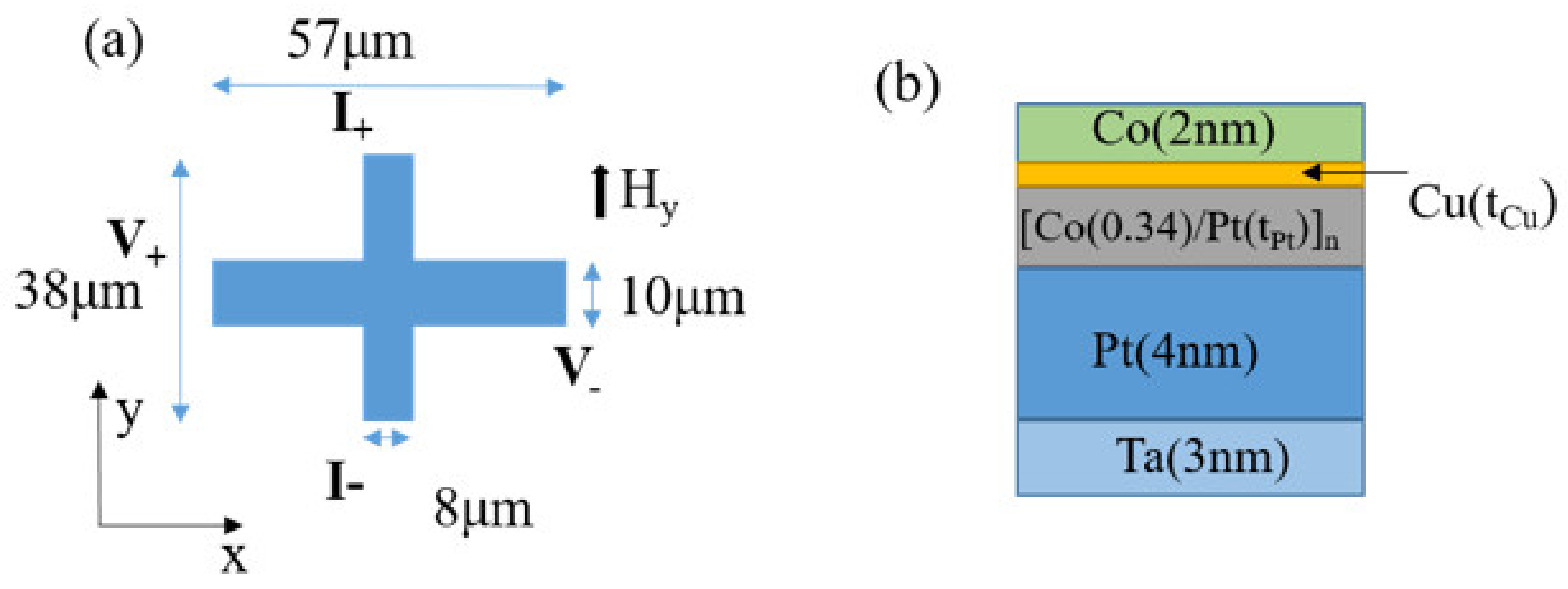
Figure 2.
Magnetization as a function of the applied field for a magnetic system of : (a) , , and , (b), , and , and (c) , , and . Inset shows probable schematic magnetic configuration in each condition.
Figure 2.
Magnetization as a function of the applied field for a magnetic system of : (a) , , and , (b), , and , and (c) , , and . Inset shows probable schematic magnetic configuration in each condition.
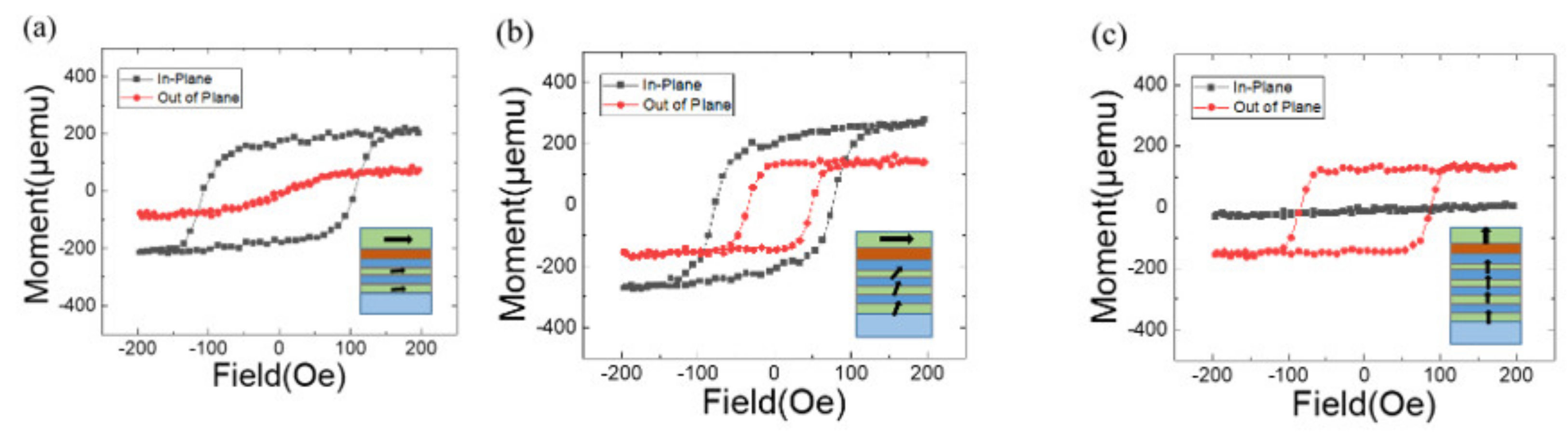
Figure 3.
Anomalous Hall resistance as a function of the applied current for a magnetic system of with , , and , under the specified external fields: (a) field along + y-axis and (b) field along – y-axis. The data is shifted off for comparison.
Figure 3.
Anomalous Hall resistance as a function of the applied current for a magnetic system of with , , and , under the specified external fields: (a) field along + y-axis and (b) field along – y-axis. The data is shifted off for comparison.
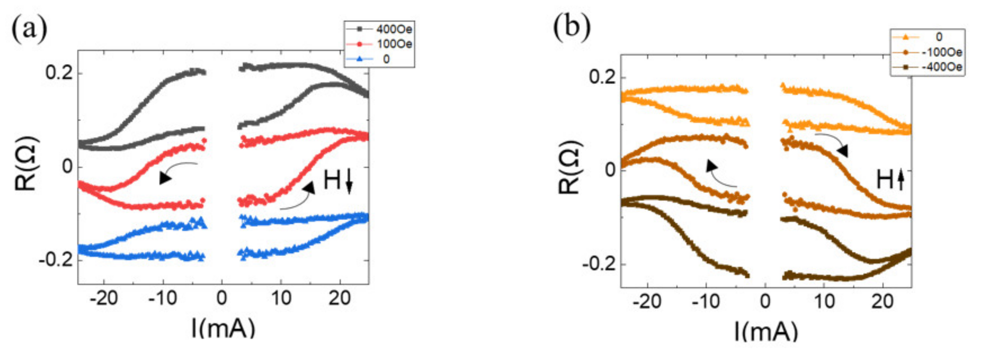
Figure 4.
Magnetization as a function of the applied field for a magnetic system of : (a) , and and (b) , and . (c) Anomalous Hall resistance as a function of the applied current with specified external fields parallel to the current direction (the y-axis) for the sample of (b). The data are shifted off for comparison.
Figure 4.
Magnetization as a function of the applied field for a magnetic system of : (a) , and and (b) , and . (c) Anomalous Hall resistance as a function of the applied current with specified external fields parallel to the current direction (the y-axis) for the sample of (b). The data are shifted off for comparison.
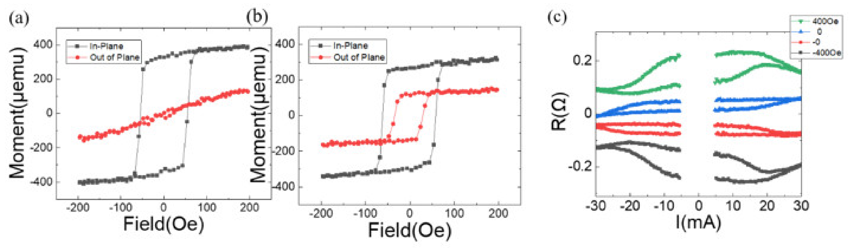
Figure 5.
Magnetization as a function of the applied field for a magnetic system of : (a) , and , and (b) , and . (c) Anomalous Hall resistance as a function of the applied current with specified external fields parallel to current direction (the y-axis) for the sample of (b). The data are shifted off for comparison.
Figure 5.
Magnetization as a function of the applied field for a magnetic system of : (a) , and , and (b) , and . (c) Anomalous Hall resistance as a function of the applied current with specified external fields parallel to current direction (the y-axis) for the sample of (b). The data are shifted off for comparison.
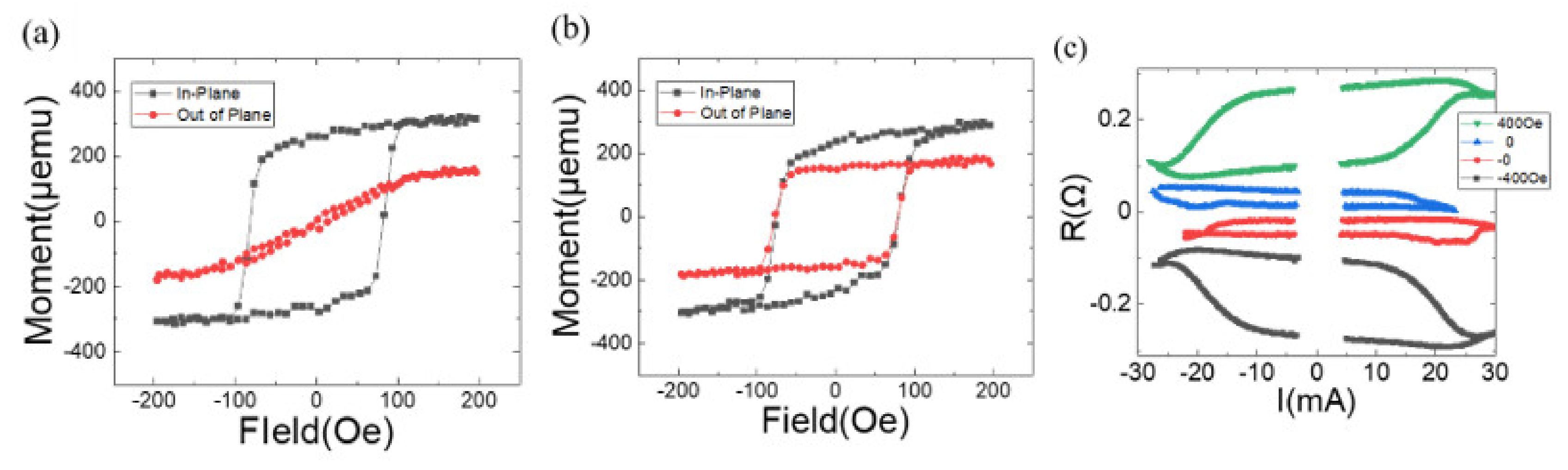
Figure 6.
Magnetic switching ratio of zero-field switching (black symbols, left vertical axis) to the magnetic full switching under a field of 400 O and critical current density (red symbols, right vertical axis) for the samples: (a) , , and , (b) , , and and (c) , , and .
Figure 6.
Magnetic switching ratio of zero-field switching (black symbols, left vertical axis) to the magnetic full switching under a field of 400 O and critical current density (red symbols, right vertical axis) for the samples: (a) , , and , (b) , , and and (c) , , and .
Disclaimer/Publisher’s Note: The statements, opinions and data contained in all publications are solely those of the individual author(s) and contributor(s) and not of MDPI and/or the editor(s). MDPI and/or the editor(s) disclaim responsibility for any injury to people or property resulting from any ideas, methods, instructions or products referred to in the content. |
© 2024 by the authors. Licensee MDPI, Basel, Switzerland. This article is an open access article distributed under the terms and conditions of the Creative Commons Attribution (CC BY) license (http://creativecommons.org/licenses/by/4.0/).
Copyright: This open access article is published under a Creative Commons CC BY 4.0 license, which permit the free download, distribution, and reuse, provided that the author and preprint are cited in any reuse.