Submitted:
05 September 2024
Posted:
05 September 2024
You are already at the latest version
Abstract
This paper details the approach to the efficient design and optimization of reversible adder and multiplier utilizing Peres gates which is a three input, three output gate. Peres gates are recognized for their universality and energy efficient properties and present an intriguing option for constructing reversible circuits. Reversible logic are characterized by its ability to uniquely determine input states from output states. The design methodology involves a cascading arrangement of Peres gates each performing a reversible XOR operation on corresponding bits of the input numbers and the carry out from the preceding stage. The paper presents a detailed schematic representation, simulation results and analysis of the proposed designs of different adders and multipliers showcasing their potential for reversible applications. The integration of Peres gates in the adder and multiplier design signifies a step forward in the exploration of reversible logic circuits and their applications in contemporary computing paradigms. The overall hardware reduction is the main achievement of this research in terms of quantum cost.
Keywords:
Carry Save Adder
; Carry Skip Adder
; Look Ahead Carry Adder
; Multiplier
; Peres Gates
; Ripple Carry Adder
; Reversible Logic
1. Introduction
The ever evolving landscape of digital computing demands innovative solutions to address the challenges posed by emerging technologies. Reversible logic has gained prominence for its unique ability to perform computations in a manner that enables the retrieval of input states from output states. The Ripple Carry Adder is a fundamental digital circuit used for binary addition. This paper explores the utilization of Peres gates in the design of a Ripple Carry Adder and Carry Save Adder aiming to leverage the reversible properties of Peres gates for potential applications in quantum computing where the preservation of information is a critical consideration. Multipliers are fundamental components in digital circuits responsible for executing arithmetic operations, with their efficiency playing a pivotal role in overall system performance. Integrating Peres gates into multiplier design offers a promising avenue for achieving both computational precision and energy efficiency.
Peres gates characterized by their reversible nature present an intriguing opportunity to create circuits that can be seamlessly integrated into the quantum computing paradigm. This paper endeavors to investigate the design and implementation of a RCA using Peres gates and the specific design methodology employed in constructing a 4x4 reversible multiplier using Peres gates aiming to harness the benefits of reversibility for enhanced computational capability.
The structure of this paper is organized as follows: Section II provides an overview of reversible logic and the unique characteristics of Peres gates. Section III details the design methodology, outlining the steps involved in constructing the RCA, CSA and multiplier using Peres gates. Section IV details the design methodology outlining the steps involved in constructing the multipliers with RCA, CSA using Peres gates. Section V presents a schematic representation of the designs illustrating the interconnection of Peres gates and input/output bits. Simulation results and analysis are discussed in Section VI highlighting the performance and potential applications of the proposed design. The paper concludes in Section VII with a summary of findings and suggestions for future research directions.
This exploration into the integration of Peres gates in a fundamental arithmetic circuit holds promise for advancing the field of reversible and quantum computing contributing to the ongoing efforts to redefine the capabilities of digital systems in the face of evolving computational paradigms.
2. Reversible Logic and Peres Gates
Reversible logic stands out in the realm of digital circuit design due to its distinctive property of information preservation allowing for computations where original input states can be uniquely reconstructed from the corresponding output states. This reversibility characteristic becomes particularly relevant in quantum computing where the conservation of information is crucial for leveraging quantum superposition and entanglement. Peres gates is particularly valuable in reversible logic design because it facilitates the creation of circuits that adhere to the principles of information conservation. Peres gate with three inputs and three outputs are as shown in Figure 1, Figure 2 and Figure 3.
Both Figure 2 and Figure 3 represents the Peres gate but the difference between these two representations is that the Peres gate in Figure 2 has gate count as 1 and number of two qubit model is 4 whereas in Figure 3 where the Peres gate is constructed using one three input Toffoli gate followed by one two input Toffoli gate has gate count as 2 and number of two qubit model is 6 [1]. All the circuits mentioned in this paper are constructed using the peres gate shown in Figure 2.
The truth table in Table 1 describes the relation between inputs and outputs. The output a is the same as the input a, output b can be obtained by logical exoring the inputs a and b whereas output c can be obtained as logical exoring of input c with logical anding of a and b i.e. (ab xor c).
In the context of the Ripple Carry Adder (RCA) design Peres gates are employed to perform reversible XOR operations which are fundamental to binary addition. The ability to selectively apply NOT operations based on control bits makes Peres gates a versatile building block for constructing circuits with minimal energy dissipation, a critical consideration in quantum and reversible computing.
The reversible nature of Peres gates ensures that the input states can be accurately reconstructed from the output states aligning with the requirements of quantum computing algorithms. The controlled NOT operation provided by Peres gates enables the creation of a coherent and efficient RCA design contributing to the exploration of reversible logic in practical applications.
This section sets the stage for the subsequent discussion on the design methodology where the unique characteristics of Peres gates are leveraged to construct a reversible Ripple Carry Adder, Carry Save Adder and reversible multipliers using these two adders. The use of reversible logic particularly through Peres gates presents an exciting avenue for the advancement of computing paradigms including quantum and emerging reversible computing technologies.
3. Design Methodology
This section details the design methods used for development of Peres Gate, Ripple carry adder and multiplier circuits including the vedic multiplier using reversible logic. The design of the Ripple Carry Adder (RCA), Carry Save Adder using Peres gates follows a systematic and staged approach leveraging the reversible nature of Peres gates to achieve an efficient and coherent circuit. The methodology involves the incorporation of Peres gates in a cascading fashion to perform reversible XOR operations on corresponding bits of the input numbers and carry outs from the preceding stages [2,3].
The design of the Ripple Carry Adder and Carry Save Adder using Peres gates follows a stage wise approach:
- First Bit (LSB): A Peres gate is employed to perform a reversible XOR operation on the least significant bits of the numbers to be added and the input carry. This stage produces the sum bit and a carry out for the next stage.
- Intermediate Bits (1 to 2*n-1): Peres gates are used in a cascading fashion where each gate performs a reversible XOR operation on the corresponding bits of the input numbers and the carry out from the previous stage. This process is repeated for the intermediate bits.
- Final Bit (MSB): The most significant bits of the input numbers and the carry out from the previous stage are fed into a Peres gate to produce the final sum bit and carry out.
The output of the RCA is the concatenation of the sum bits (S[2*n-1:0]). The final carry out (Cout_n) serves as an overflow indicator providing information about whether the addition operation resulted in a carry beyond the designated bit size.
Peres gates which belong to the class of three input quantum gates have shown promise in implementing various logical functions and we focused on utilizing Peres gates to design a 4x4 reversible multiplier. Peres gates introduced by Asher Peres in 1984 have been recognized for their universality meaning they can be used to construct any reversible circuit. This characteristic makes Peres gates an attractive choice for designing complex reversible circuits such as multipliers. The 2x2 and 4x4 reversible multipliers are constructed using a combination of Toffoli gates and Peres gates.
The simplest form of multiplier circuit formed as a 1-bit multiplier is with a single Peres gate with multiplicand as a0 and multiplier as bo and the third input given to the Peres gate will be the product result as the output given by c0 as shown in Figure 4. The product obtained at the output is 0 when multiplicand a0 is 0 or multiplier b0 is 0 and the maximum value of product is 1 when both a0 and bo are at logic 1.
In Figure 5 the variable a is considered to be multiplicand and variable b as multiplier. The product of two bit number is 0 when the multiplier is 0 and multiplicand has any value between 0 and 3 whereas the maximum value of the product will be 6 when both multiplicand and multipliers has decimal value 3 or “11” in binary format.
4. Schematic Representation
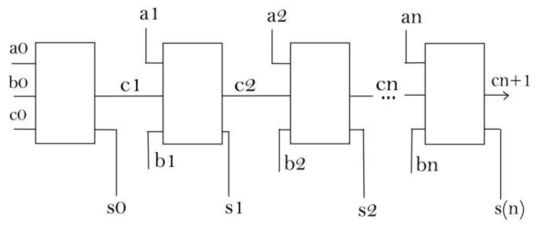
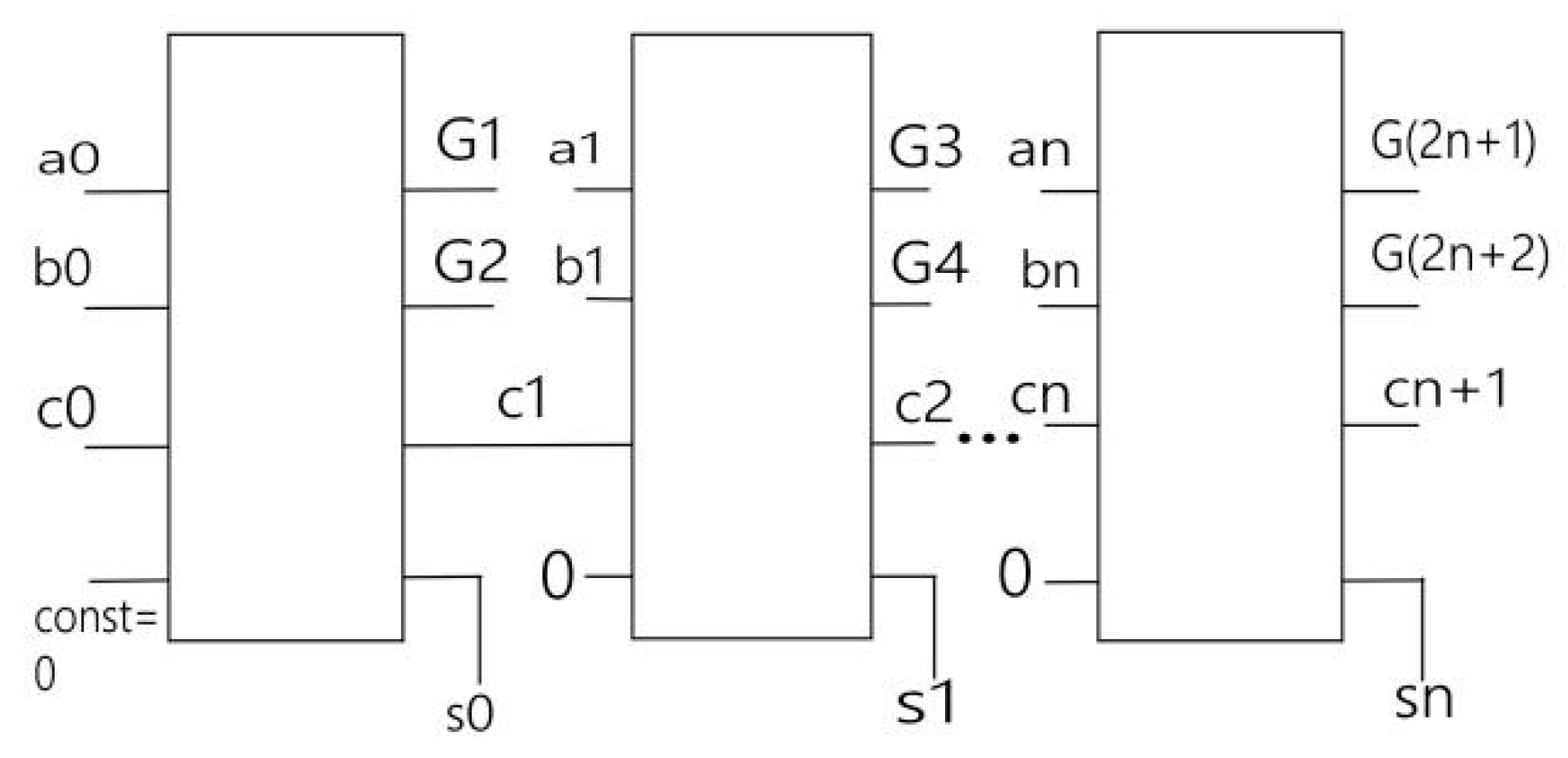
A schematic diagram visually represents the connections between Peres gates, input bits (A, B), carry ins, carry outs and the sum bits. The cascading arrangement of Peres gates highlights the systematic application of reversible XOR operations at each stage ensuring the overall circuit adheres to the principles of reversible logic. The use of Peres gates in this design methodology not only ensures reversibility but also opens the door to potential applications in quantum computing due to their inherent characteristics of information preservation. This design methodology forms the foundation for the subsequent sections where a detailed schematic representation, simulation results and analysis will be presented to validate the functionality and performance of the proposed Ripple Carry Adder using Peres gates. A schematic diagram illustrates the connections between Peres gates, input bits and carry outs at each stage as depicted in Figure 6 and Figure 7. The reversible nature of Peres gates allows for a coherent design that ensures the reversibility of the overall circuit.
The schematic representation visually captures the interconnection of Peres gates, input bits (A, B), carry ins (Cin), and carry outs (Cout) at each stage of the Ripple Carry Adder (RCA). The design utilizes Peres gates for reversible operations ensuring information conservation throughout the addition process.
The connections illustrate the systematic application of Peres gates where each gate performs a reversible XOR operation on the corresponding bits of the input numbers and the carry out from the previous stage. The final sum bits (S[n:0]) and carry out (Cout_n) collectively form the output of the RCA as shown in Figure 10. The cascading arrangement of Peres gates signifies the stepwise progression through the bits of the input numbers ensuring a coherent and reversible addition process. The external control lines represent the controlled NOT operation applied by the Peres gates based on input bits.
Figure 8.
A 4- level decomposition of this 2-bit vedic multiplier.
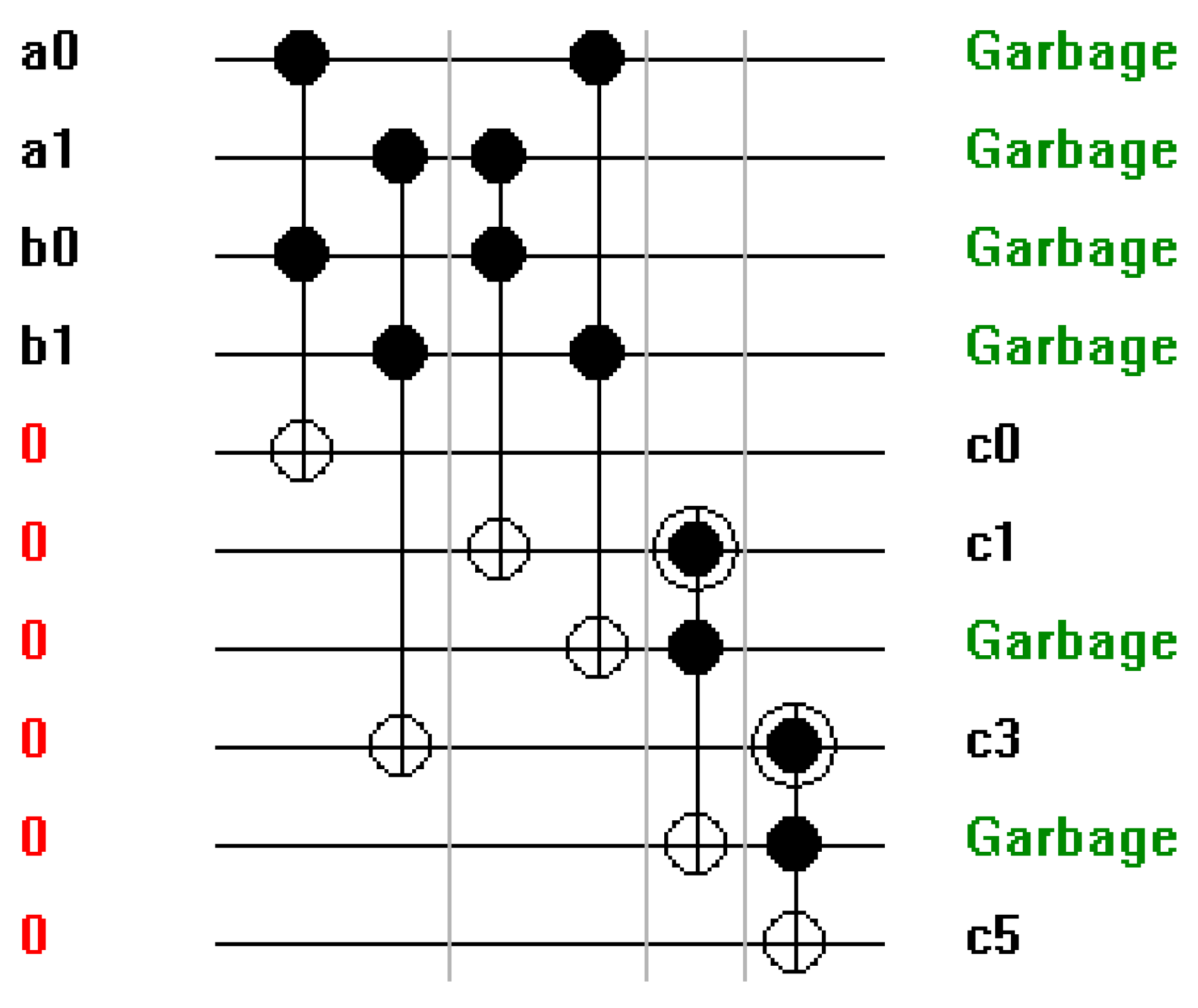
Figure 9.
Full Adder using two peres gates.
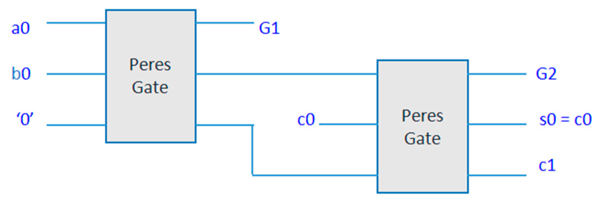
Figure 10.
1-bit adder block schematic using peres gates.
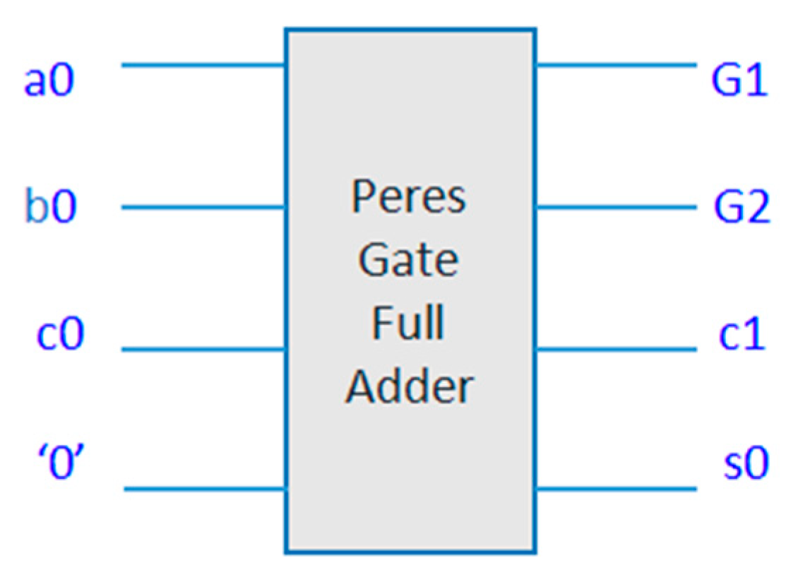
Figure 11.
1-bit adder quantum circuit using Peres Gates.
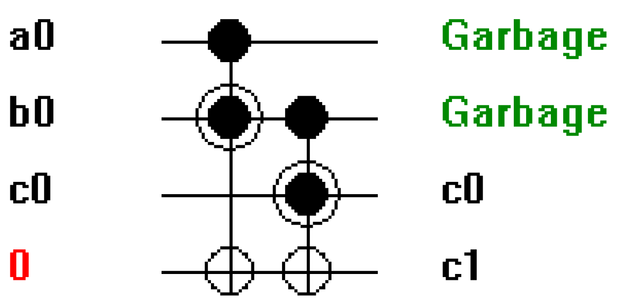
Figure 12.
Generalized Block schematic representation of n-bit ripple carry adder.
This schematic representation provides a clear visualization of the reversible logic design showcasing the utilization of Peres gates to achieve information preserving binary addition. The subsequent sections will delve into the simulation results and analysis further validating the functionality and performance of the proposed Ripple Carry Adder using Peres gates.
Figure 13.
Block schematic representation of n-bit ripple carry adder using Peres gates.
5. Simulation and Analysis
The designed circuit is simulated to validate its functionality and to analyze the performance in terms of speed and quantum cost. The simulation results demonstrate the successful addition of binary numbers with reversible characteristics.
The proposed Ripple Carry Adder (RCA) design utilizing Peres gates has been subjected to rigorous simulation to evaluate its functionality and performance for different configurations as 1-bit, 4-bit, 8-bit and 16-bit addition as shown in Figure 14 (a-d) respectively. The analysis encompasses key aspects such as speed, quantum cost adhering to the principles of reversible logic.
The simulation of the proposed Ripple Carry Adder (RCA) design using Peres gates was conducted with meticulous attention to detail, employing a comprehensive simulation setup. The objective was to validate the functionality and assess the performance of the reversible circuit under various input conditions. The designs were simulated using RCViewer+ and ModeSim- Intel FPGA starter Edition 10.5b incorporating models of Peres gates and relevant circuit elements for 1,4,8,16 bit adders, 1,2,4 bit multipliers and 2,4 bit vedic multipliers. Simulations were executed with various input scenarios covering a range of binary input cases including cases with and without carry in with adders.
5. Functionality Verification
The functionality of the Ripple Carry Adder (RCA) design using Peres gates was rigorously verified through simulation, encompassing a range of input scenarios. The simulation results confirm the correct operation of the RCA producing accurate sum bits (S[n:0]) and carry out (Cout_n) for different input combinations. The results confirm the adherence to reversible logic principles and the preservation of information throughout the addition process. The simulation results demonstrate that the sum bits (S[n:0]) produced by the RCA accurately reflect the binary addition of the input numbers (A and B) and the carry in (Cin). Each Peres gate strategically placed in the circuit performs a reversible XOR operation contributing to the generation of the sum bits.
The carry out (Cout_n) serves as an overflow indicator revealing whether there is a carry beyond the most significant bit. Simulation results affirm that the circuit correctly calculates Cout_n based on the input numbers and carry ins providing crucial information about the completion of the addition operation.
Data Collection
Data collected during the simulations including verified truth table, waveform, timing diagrams and quantum cost metrics were stored and analyzed to draw meaningful insights into the behavior of the RCA using Peres gates. The simulation setup serves as a crucial foundation for the subsequent analysis, providing a detailed understanding of how the proposed reversible circuit performs under different conditions and shedding light on its potential advantages in reversible and quantum computing applications.
The reversibility of the circuit is a fundamental aspect validated during functionality verification.
The Peres gates by design enable the reconstruction of input states from output states. Simulation results confirm that the RCA and multiplier design exhibits reversibility aligning with the principles of reversible logic.
The controlled NOT (CNOT) operation performed by Peres gates was examined through simulation ensuring that the
NOT operation is selectively applied based on the control bits. The controlled nature of the XOR operations ensures that information is not lost during the addition process. The overall functionality verification provides confidence in the correct operation of the designed RCA and multipliers using Peres gates. The subsequent sections delve into the performance analysis including considerations of speed, quantum cost and comparative assessments with traditional non-reversible designs.
Figure 15.
4X4 multiplier configurations using Toffoli and Peres Gates.
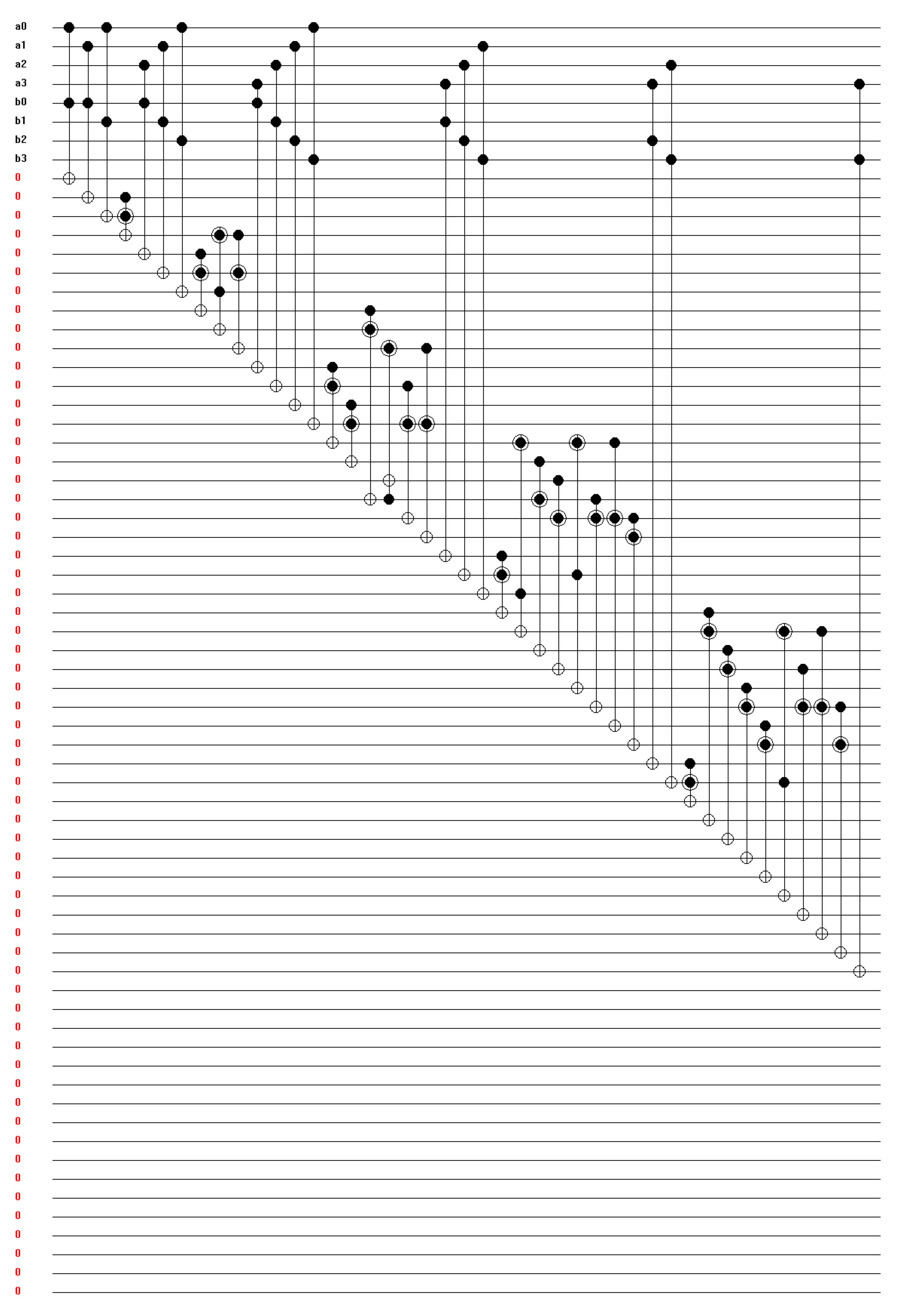
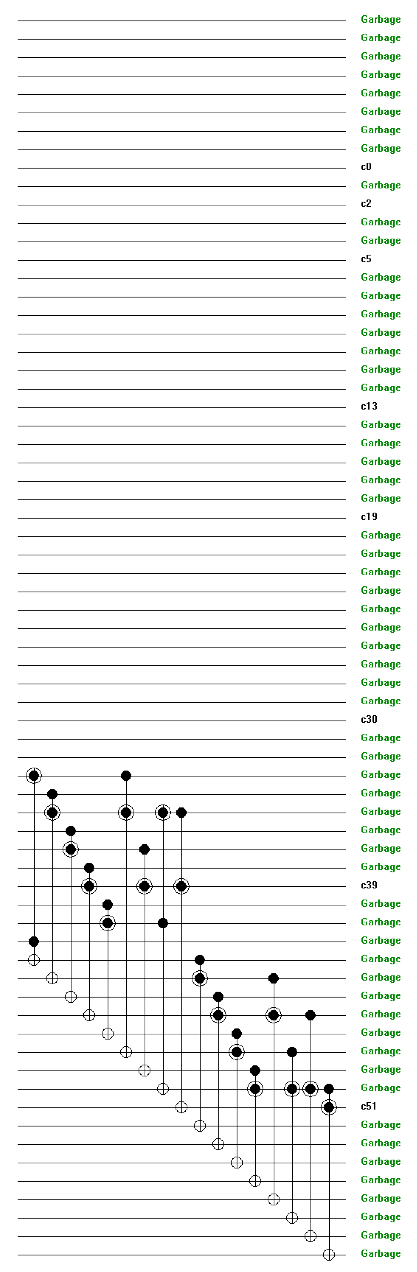
Figure 16.
Level wise decomposition of multiplier configurations using Toffoli and Peres Gates.
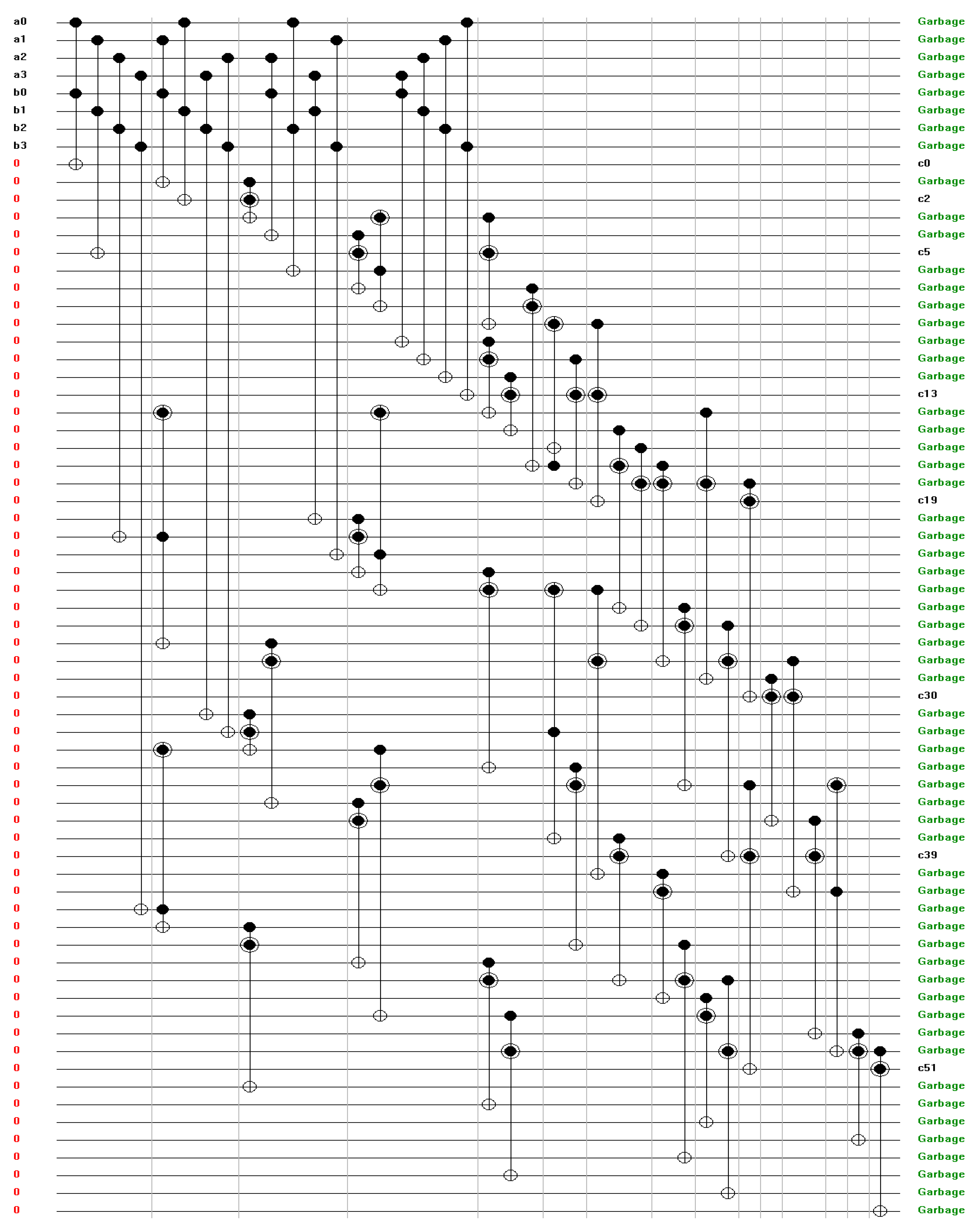
Figure 17.
(a-f) Different 4-bit adder and multiplier configurations using Toffoli and Peres Gates. a. 4-bit Ripple Carry Adder. b. 4-bit Carry Look Ahead Adder. c. 4-bit Carry Save Adder. d. 4-bit Carry Skip/Bypass Adder. e. 4-Bit Multiplier Using Ripple Carry Adder. f. 4-Bit Multiplier Using Carry Save Adder.
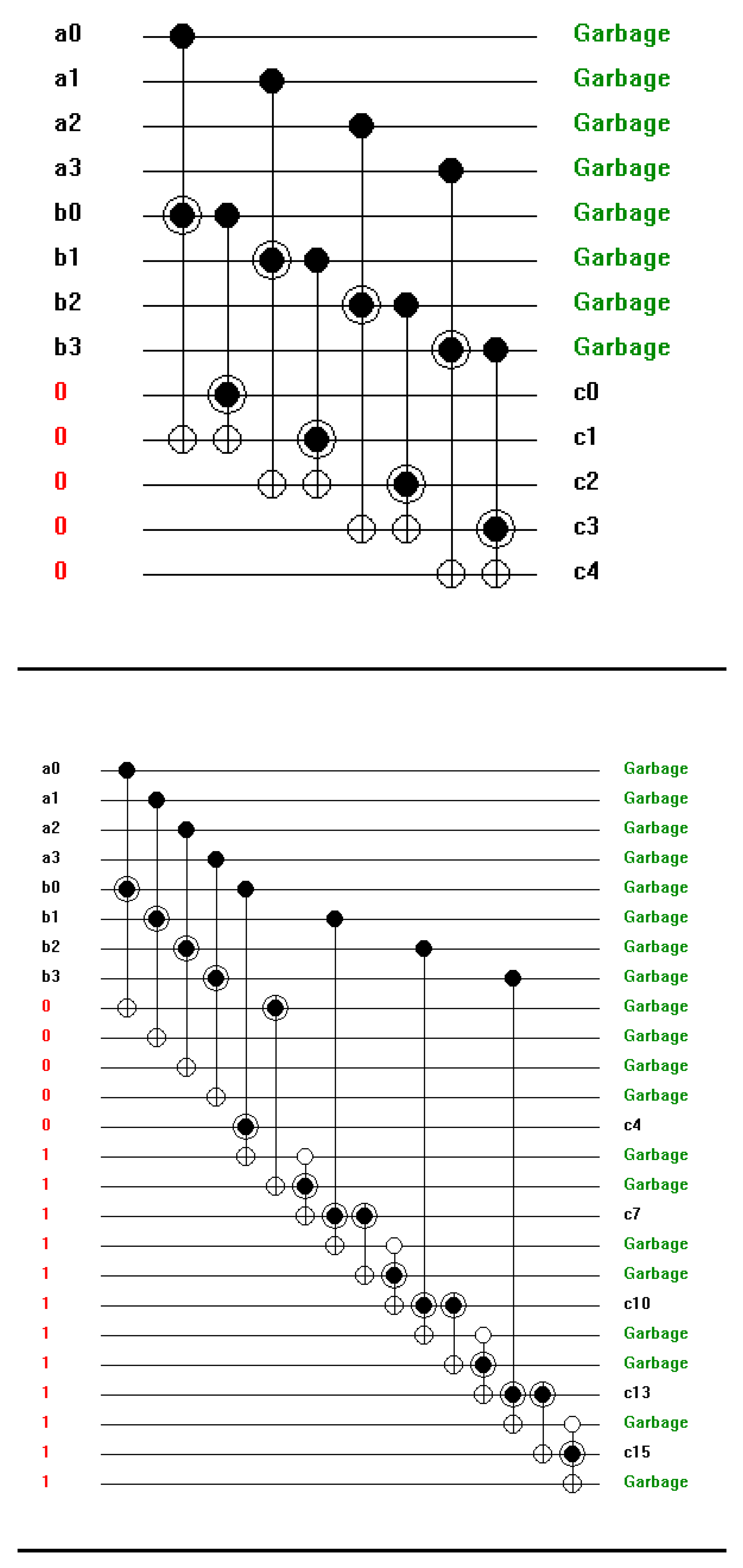
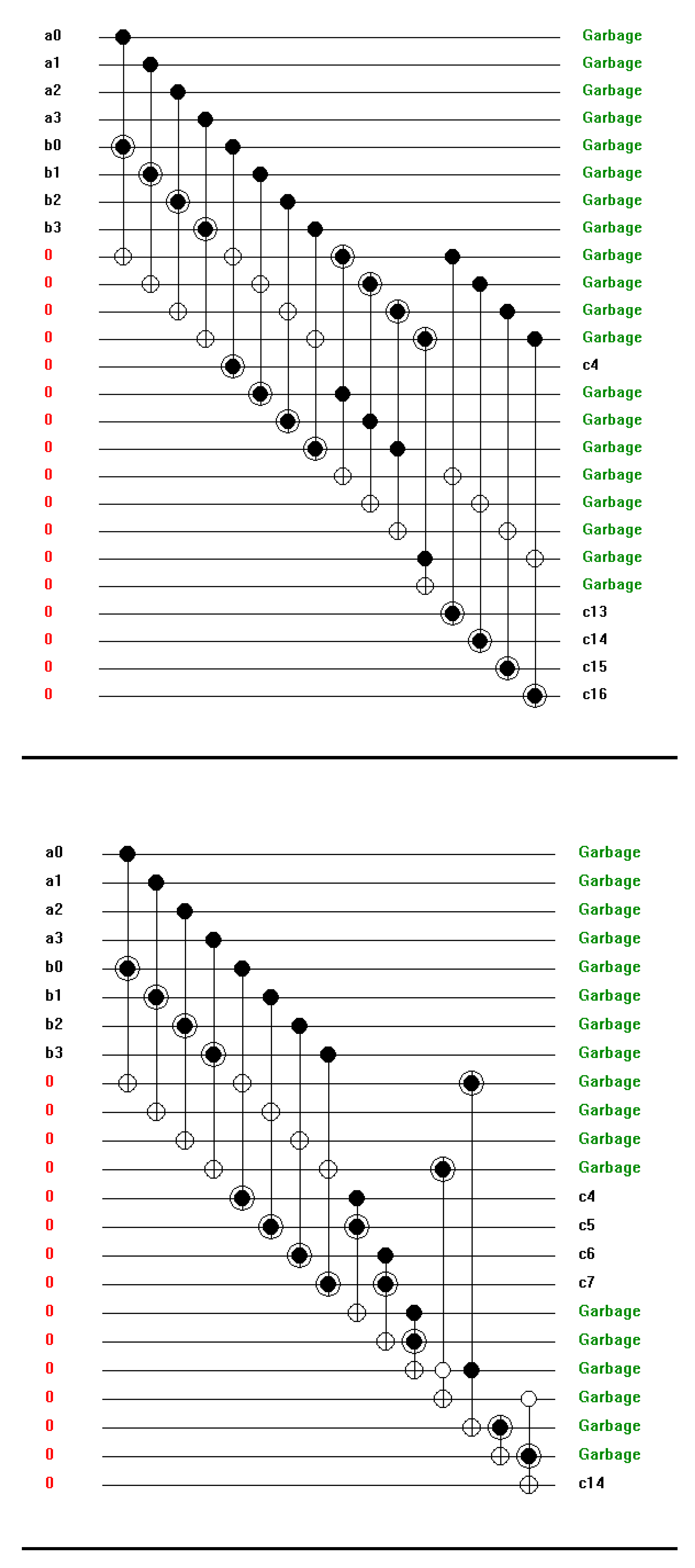
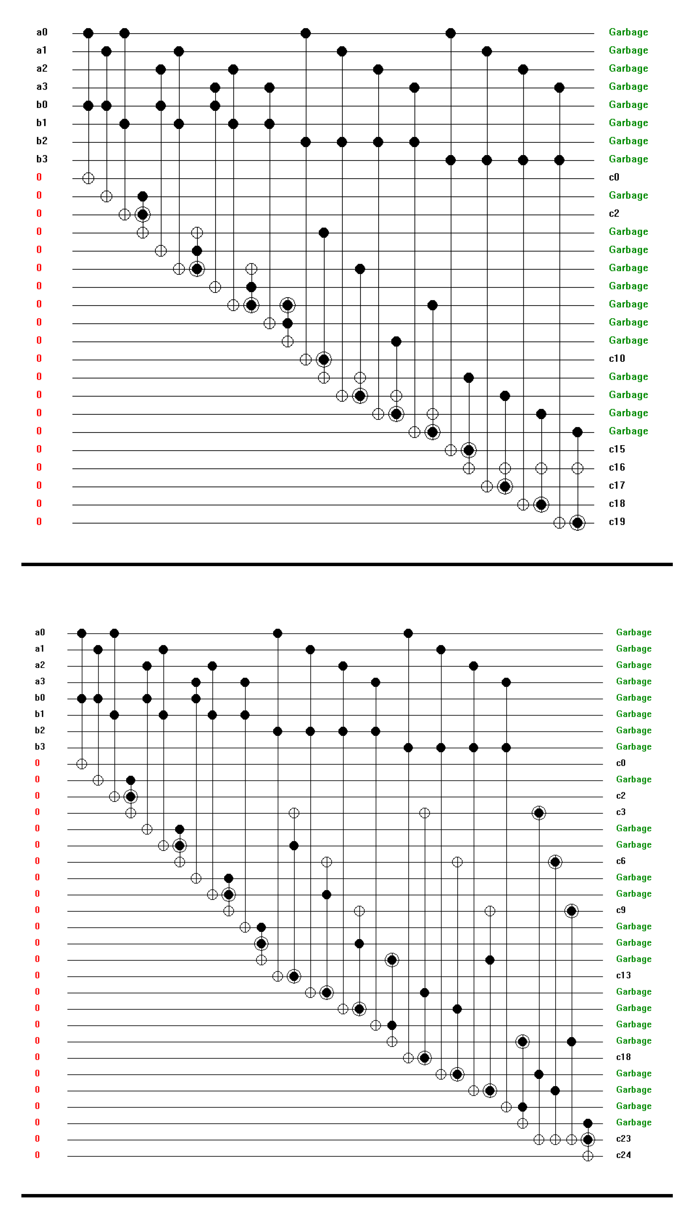
Figure 18.
Simulation result for Peres Gate.
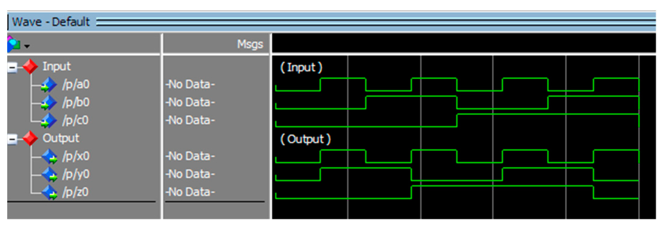
Figure 19.
Simulation result for 1-bit full adder.
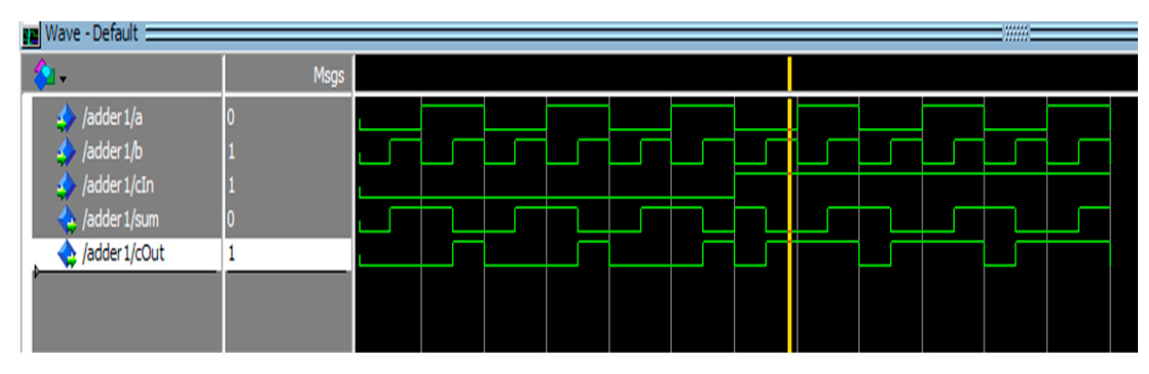
Figure 20.
Simulation result for 4-bit full adder.
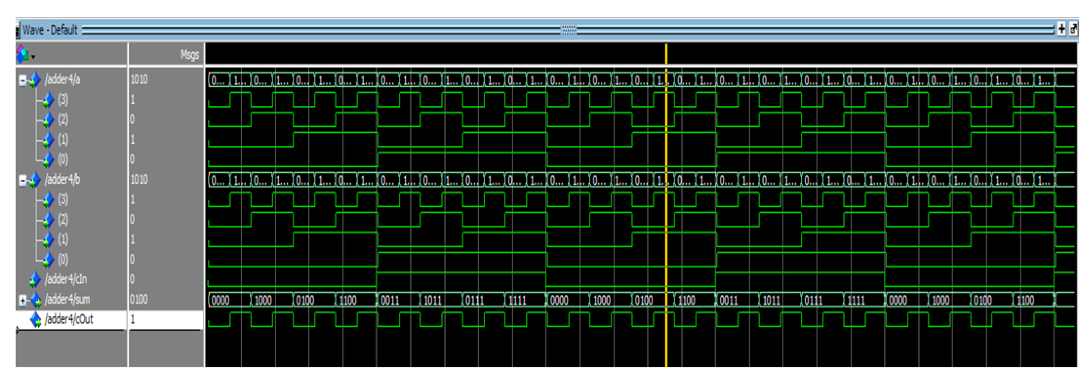
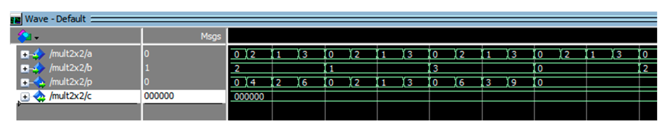
Figure 21.
Simulation result for 2-bit multiplier.
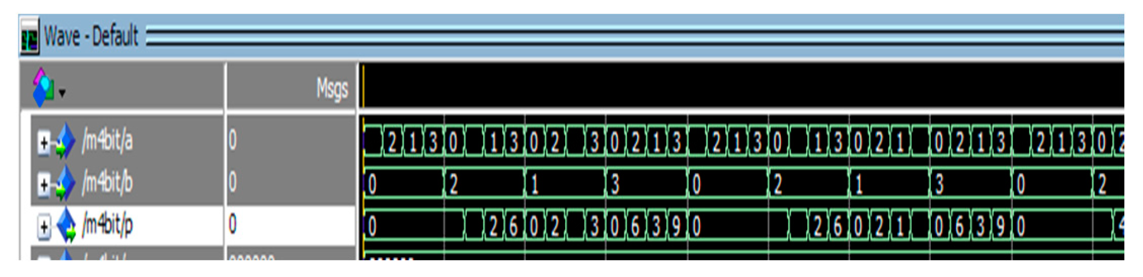
Figure 22.
(a,b) Simulation results for 4-bit multiplier (a) and (b) for different input combinations.
Figure 22.
(a,b) Simulation results for 4-bit multiplier (a) and (b) for different input combinations.
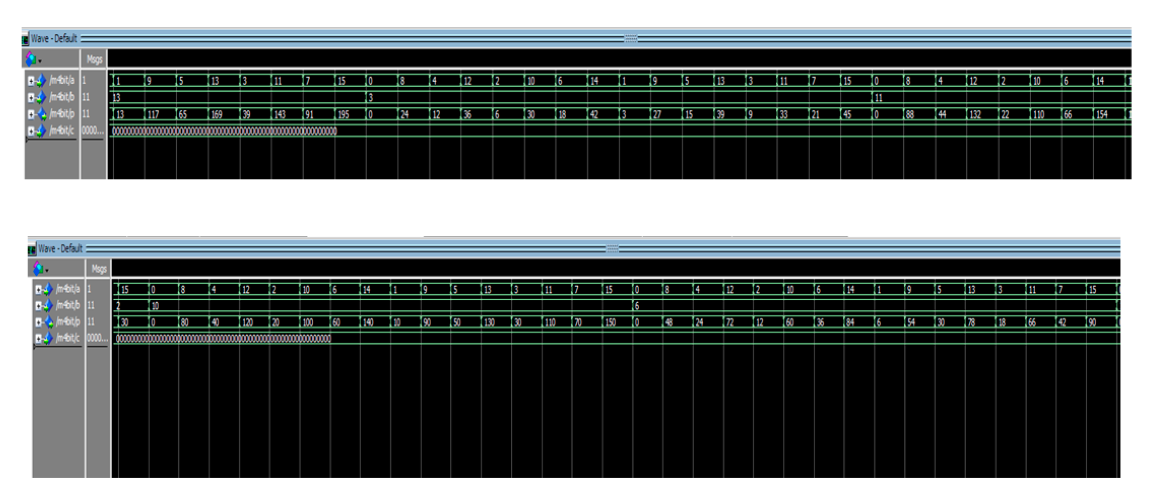
Figure 23.
Simulation result for 2-bit vedic multiplier.
From Figure 26, referring to 1-bit, 4-bit, 8-bit and 16-bit adder configurations verified using RCViewer+ and ModeSim- Intel FPGA starter Edition 10.5b, we can easily develop the following expressions as given below.
-The number of inputs/outputs (n) are calculated as
N= n *3 +1
Where n- number of bits for the adder (in our case 1,4,8,16,….)
-The number of garbage lines (g) can be calculated as g= 2*n
-The number of constant lines c=n
-The number of gates(Gate count) required for constructing adder is calculated as GC=2*n
-The number of two qubit gates(TQ) are given by TQ=8*n
-And finally the quantum cost (QC) is calculated by QC=8*n
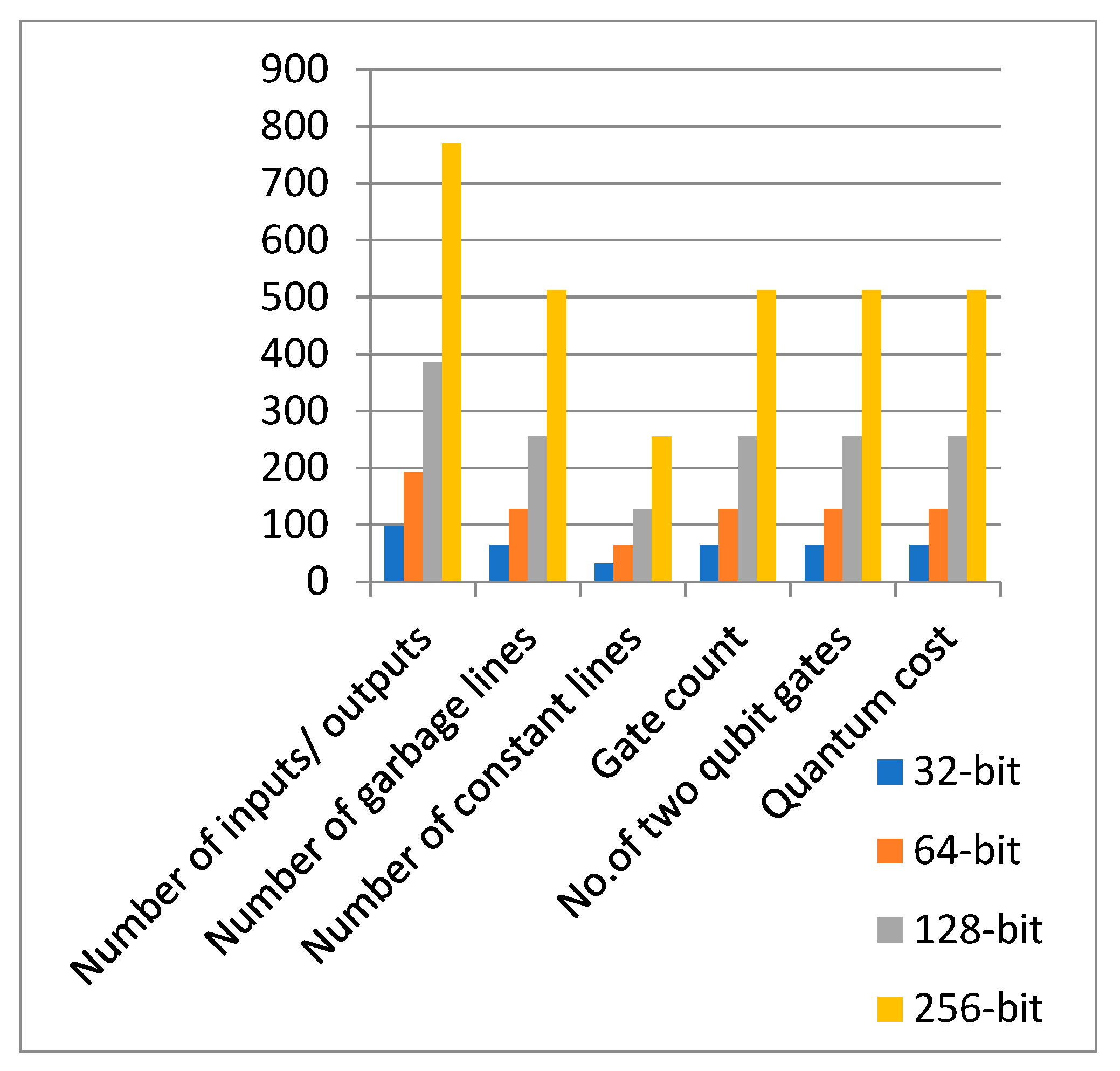
And hence by using above equations we can easily verify the following further adder configurations as shown in Figure 27.
Figure 26.
Performance analysis of Different adder configurations using Peres gates.
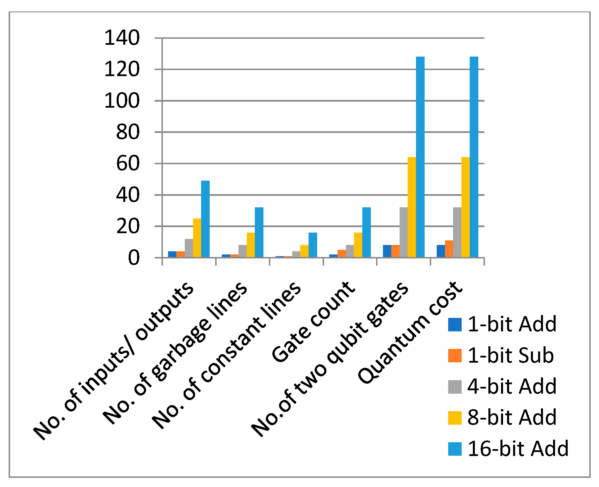
Figure 27.
Further Performance analysis of Different adder configurations using Peres gates.
A comparative analysis was conducted between the proposed reversible design and other reversible designs available in literature. This analysis considered factors such as gate count, energy consumption and overall circuit complexity.
The goal was to highlight the potential advantages of the reversible approach especially in terms of information preservation and resource utilization. Quantum speedup potential which is a measure of how much faster a quantum algorithm could perform a specific task compared to its classical counterpart was explored. The inherent reversibility of the designed circuit using Peres gates positions it favorably for potential quantum speedup in certain algorithms contributing to the broader understanding of reversible logic in quantum computation. After comparing all the reversible adders using different techniques, we can say that the ripple carry adder is best suited due to the low metric values as mentioned in Figure 28. The less number of inputs, constant and garbage lines, quantum cost requirement to design adder circuit are advantageous to use ripple carry adder.
In Table 2, various reversible logic gates used are Feynman Gate(FG), Toffoli Gate(TG), Fredkin Gate(FRG), Peres Gate(PG), New Gate(NG), TSG Gate(TSG), MKG Gate(MKG), HNG Gate(HNG), PFAG Gate(PFAG) for comparison on the number of gates used for the construction of different reversible multiplier configurations. First three multiplier circuits are designed as a part of research in this research article using only Toffoli and Peres Gates. The other comparative circuits used other reversible gates available in literature as shown in the table. In Figure 29 the comparison of different multiplier circuits is made in the basis of quantum cost. The 4-bit reversible multiplier proposed in this article has comparable quantum cost as compared to other multiplier circuits. The reduced quantum cost as 256 is the main outcome of this research as compared to more quantum cost for the same circuit design in literature.
The analysis also considered potential optimization opportunities for the design. This includes exploring advanced reversible gates, circuit restructuring or algorithmic enhancements to further improve performance metrics and address any identified limitations. The comprehensive evaluation of performance metrics provides valuable insights into the strengths and potential areas of improvement for the RCA design using Peres gates. The outcomes of these analyses contribute to the broader understanding of reversible logic circuits and their applications in emerging computational paradigms. In Figure 30, Levels 1,2 and 3 on Y-axis represents Low, Moderate and High levels respectively. From this figure we can conclude that the vedic multiplier the best reversible multiplier with low gate count, quantum cost, gate level delay, hardware complexity, scalability, area and number of Ancilla bits with high garbage outputs which can be neglected as the reversibility efficiency provided by this circuit is high. The ripple carry adder constructed using reversible logic has all metrics considered to be at moderate level, but it provides higher gate level delays which can be neglected as the hardware complexity and area in terms of gates is also less.
After examining all the adders and multiplier circuits using Toffoli and Peres gates, a comparison table for designing various adders and multipliers using reversible logic is prepared and presented in terms of a chart as shown in Figure 30. The key parameters considered in the design of reversible circuits includes all the metrics used measure the performance of these circuits.
As a matter of facts the reversible ripple carry adder is suitable for low power applications but has higher delay due to the sequential carry propagation. The reversible carry look-ahead adder is faster than ripple carry due to parallel carry calculation but requires more gates and garbage outputs. The reversible carry save adder is used in multi-operand addition scenarios like in multipliers but with higher complexity. The reversible multiplier is simple design but has high gate count and quantum cost. The reversible adder and multiplier design using vedic mathematics are optimized for high-speed operations but at the cost of significantly increased hardware complexity and power consumption.
7. Future Considerations
While the current simulations provide promising results, further optimizations and exploration of advanced reversible logic gates could enhance the overall performance of the design. Additionally the integration of the proposed design into larger circuits and quantum algorithms warrants investigation for its scalability and applicability. There might be different opportunities for optimizing the circuit design including the investigation of advanced reversible gates and alternative architectures that may further enhance the efficiency and speed of the RCA. The integration of the designed circuit into quantum algorithms assessing its compatibility and efficiency in specific quantum computing applications can be investigated. Explore how the reversibility of the circuit can contribute to quantum speedup in relevant algorithms. The scalability of the proposed design can be assessed by exploring its integration into larger circuits and arithmetic units.
These future considerations aim to extend the impact of the current research fostering a deeper understanding of reversible logic circuits and their potential applications in the rapidly evolving fields of quantum and reversible computing.
8. Conclusions
The simulation and analysis affirm the functionality and potential advantages of the adders and multipliers design using Peres gates and are efficient and information preserving circuits. The reduction in quantum cost about 10% to 48% for 4-bit multipliers with ripple carry adder and carry save adder using Peres gates comparing literature circuits is the main outcome of this research.
Acknowledgments
The authors would like to acknowledge G.H. Raisoni College of Engineering and Management, Wagholi, Pune and Sinhgad Institute of Technology and Science, Narhe, Pune for providing resources and support for this research.
References
- Thapliyal H and Ranganathan N 2010 Design of reversible sequential circuits optimizing quantum costs, delay, and garbage outputs, ACM J. Emerg. Technol. Comput. Syst. 6, 4, Article 14. [CrossRef]
- Rohit Kumawat and Trailokya Nath Sasamal 2016 Design of 1-bit and 4-bit Adder using Reversible Logic in Quantum-Dot Cellular Automata, IEEE International Conference On Recent Trends In Electronics Information Communication Technology.
- Waje M G and Dakhole P K 2013 Design and implementation of 4-bit arithmetic logic unit using quantum dot cellular automata, Proc. IEEE 3rd IACC 1022-1029.
- Kunalan D. Cheong C L Chau C F and Ghazali A B 2014 Design of a 4-bit adder using reversible logic in quantum-dot cellular automata (QCA), Proc. IEEE ICSE 60-63 9. Mollem P and Eshanpour M 2013.
- A Novel Design of Reversible Multiplier, International Journal of Engineering, IJE Transaction C:Aspects Vol. 26 No. 6: 577-586Mollem P and Eshanpour M 2013 A Novel Design of Reversible Multiplier, International Journal of Engineering, IJE Transaction C:Aspects Vol. 26 No. 6: 577-586.
- Mohammadi M Navi K. and Eshghi M 2009 Optimized reversible multiplier Circuit, Journal of Circuits, Systems and Computers Vol. 18 No. 2: 311-323. [CrossRef]
- Islam M S Rahman M M Begum Z and Hafiz M Z 2009 Low cost quantum realization of reversible multiplier circuit, Information Technology Journal Vol. 8 No. 2: 208-213. [CrossRef]
- Shams M Haghparast M and Navi K 2008 Novel reversible multiplier circuit in nanotechnology, World Appllied Science Journal Vol., No. 5: 806-810.
- Thaplyal H and Srinivas M B 2006 Novel reversible multiplier architecture using reversible TSG gate, IEEE International Conference on Computer Systems and Applications 100-103.
- Thaplyal H Srinivas M B and Arabnia H R 2005 A reversible version of 4x4 bit array multiplier with minimum gates and garbage outputs, International Conference on Embedded System and Applications (ESA'05) Las Vegag USA 106-114.
- M. Shams, M. Haghparast and K. Navi, Novel reversible multiplier circuit in nanotechnology, World Appl. Sci. J. 3 (2008) 806–810.
- M. Haghparast, S. J. Jassbi, K. Navi and O. Hashemipour, Design of a novel reversible multiplier circuit using HNG gate in nanotechnology, World Appl. Sci. J. 3 (2008) 974–978.
- Shiam-Rong Kuang, Chun-Yi Wang, Ven-Jui-Chen, ALow-Cost High-Speed Radix-4 Montgomery modularmultiplier without carry-propagate format conversion, Engineering Science and Technology, an InternationalJournal, 54(2024) 101703. [CrossRef]
- Thapliyal H and Ranganathan N 2010 Design of reversible sequential circuits optimizing quantum costs, delay, and garbage outputs, ACM J. Emerg. Technol. Comput. Syst. 6, 4, Article 14.
- Asher Peres, Quantum Theory: Concepts and MEthods(Fundamental Theories of Physics, Springer Science + Business media LLC, Kluwer Academic Publishers, ISBN:0-792-33632-1.
Figure 1.
Peres Gate.
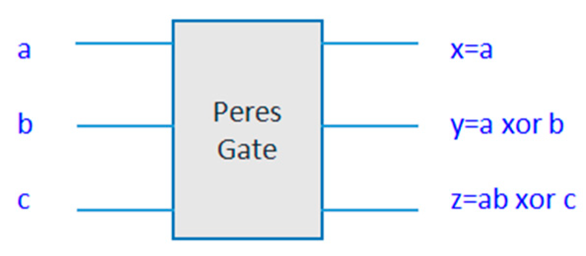
Figure 2.
Peres gate quantum circuit.
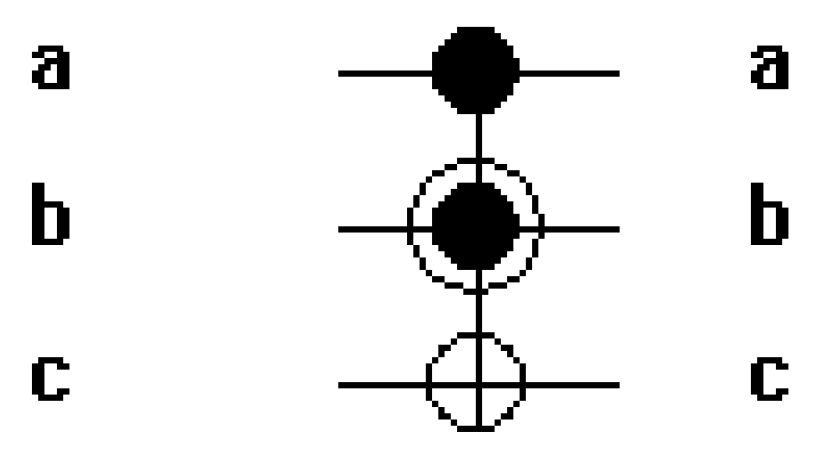
Figure 3.
Peres gate quantum circuit using two Toffoli gates.
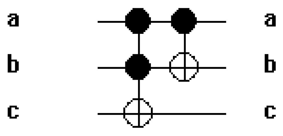
Figure 4.
1-bit multiplier.
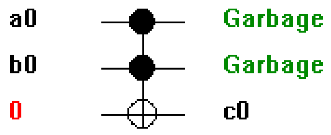
Figure 5.
A 2-bit multiplier quantum circuit using Peres Gates.
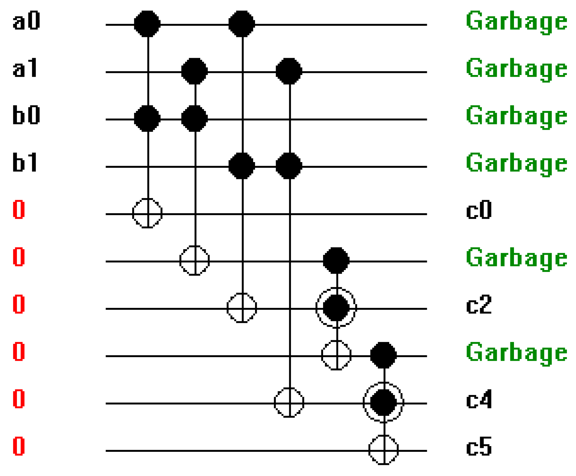
Figure 6.
A 4- level decomposition of this 2-bit multiplier.
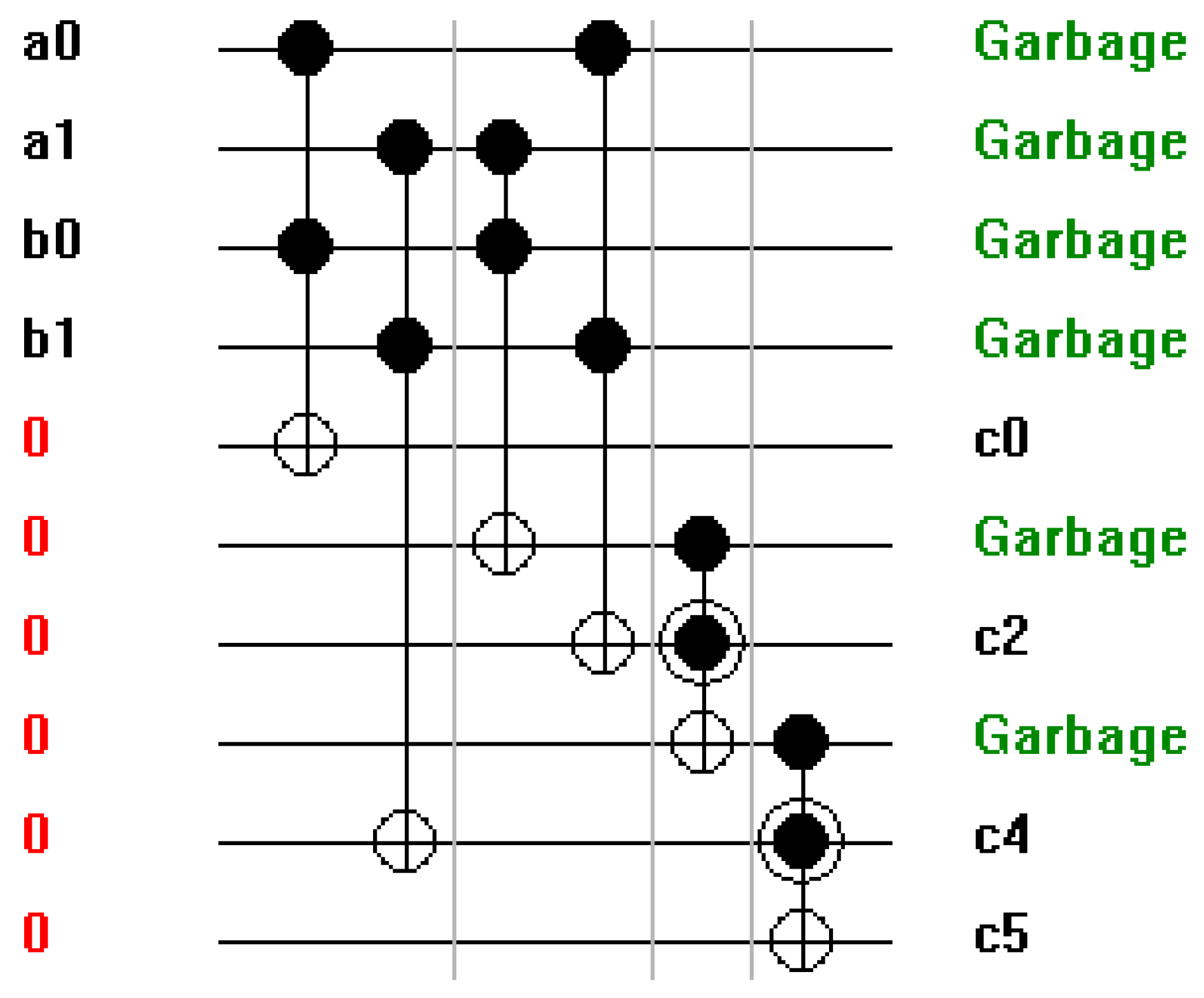
Figure 7.
A 2-bit vedic multiplier quantum circuit using Peres Gates.
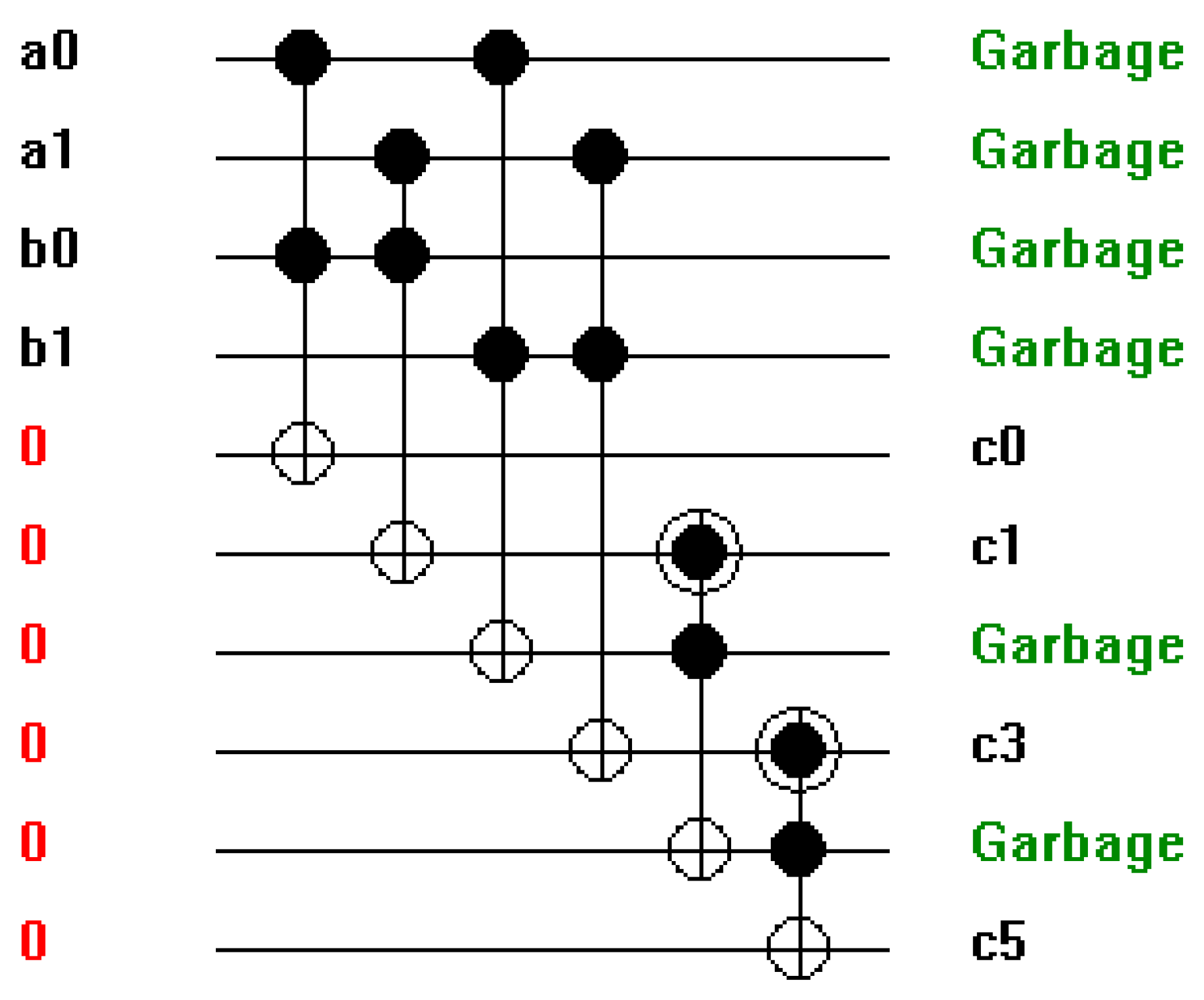
Figure 14.
a,b,c,d. Adder configurations using Toffoli and Peres Gates (a) 1-bit adder, (b) 4-bit adder, (c) 8-bit adder, and (d) 16-bit adder.
Figure 14.
a,b,c,d. Adder configurations using Toffoli and Peres Gates (a) 1-bit adder, (b) 4-bit adder, (c) 8-bit adder, and (d) 16-bit adder.
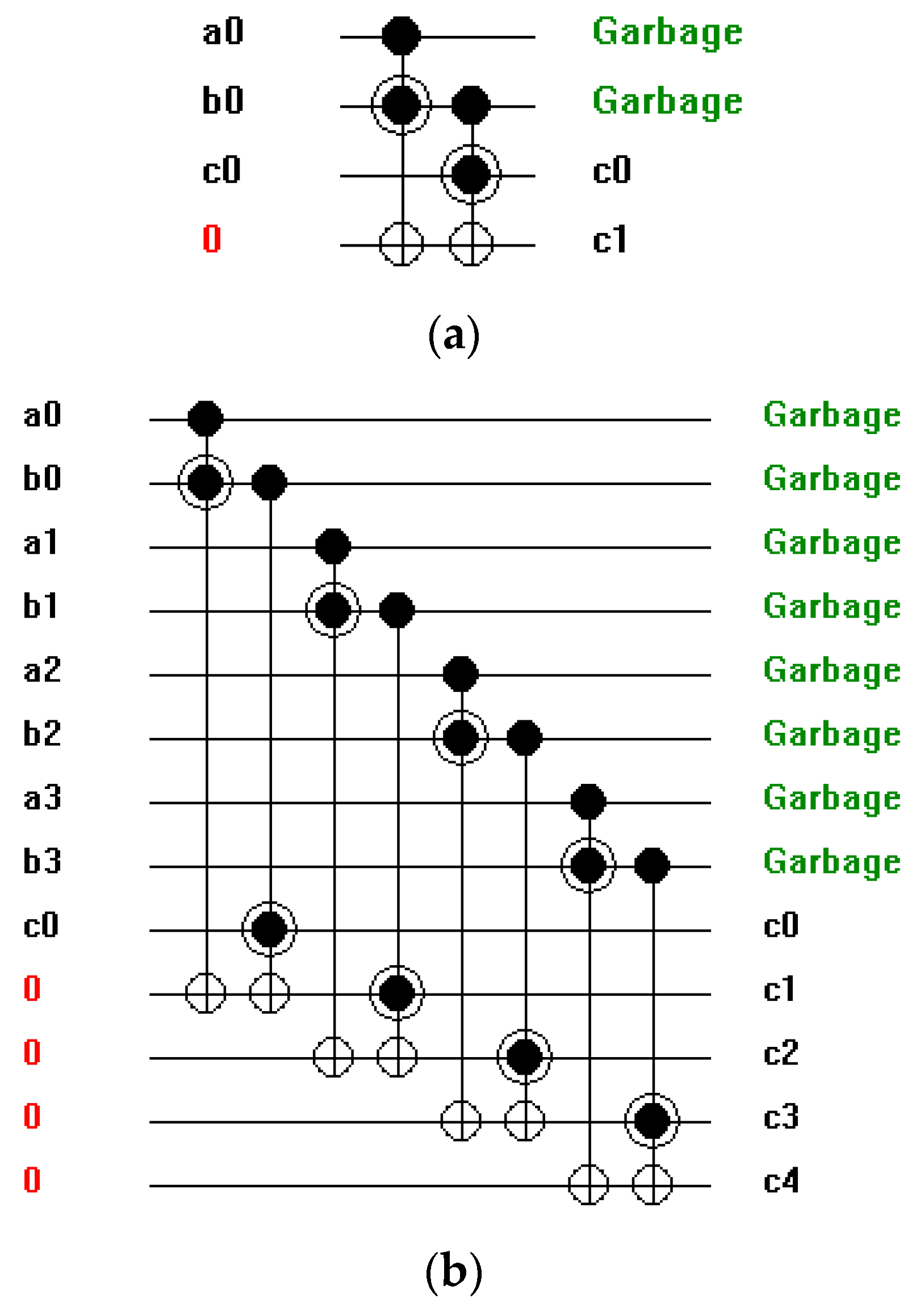
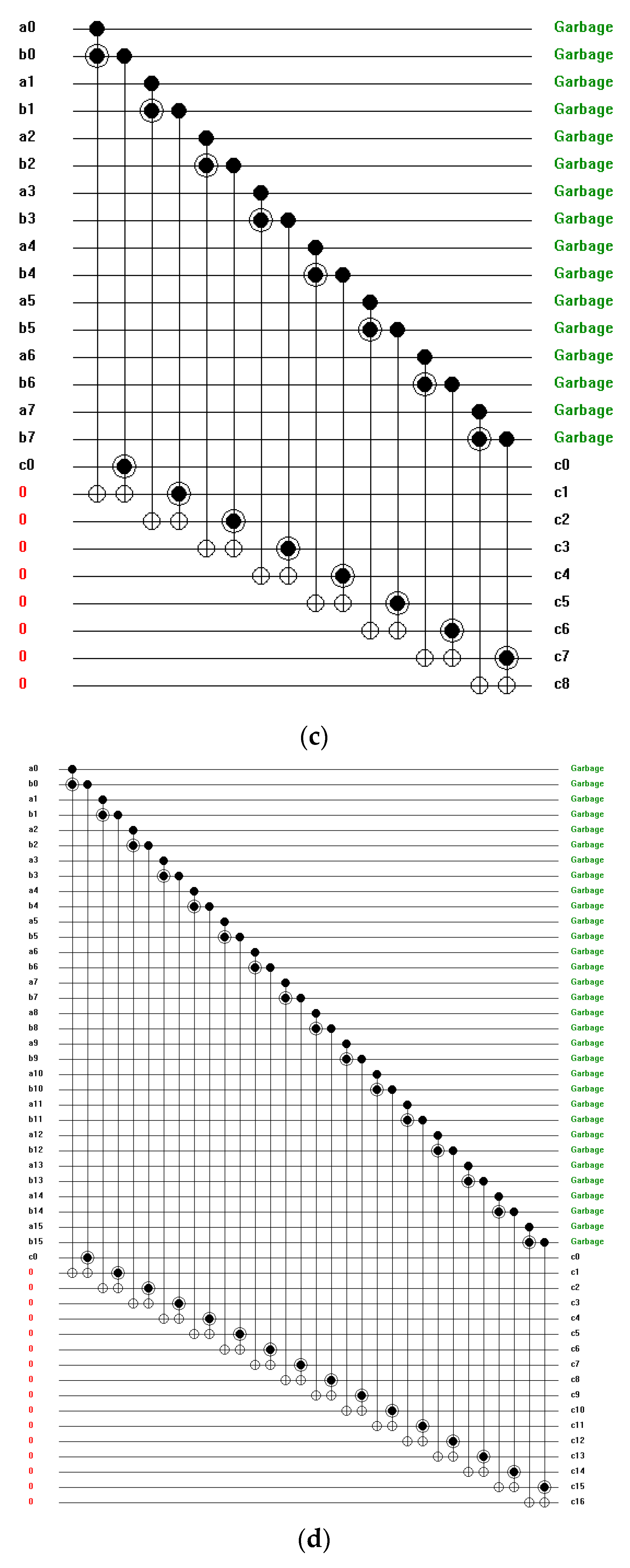
Figure 28.
Analysis of Different Adder Configurations using Peres Gates.
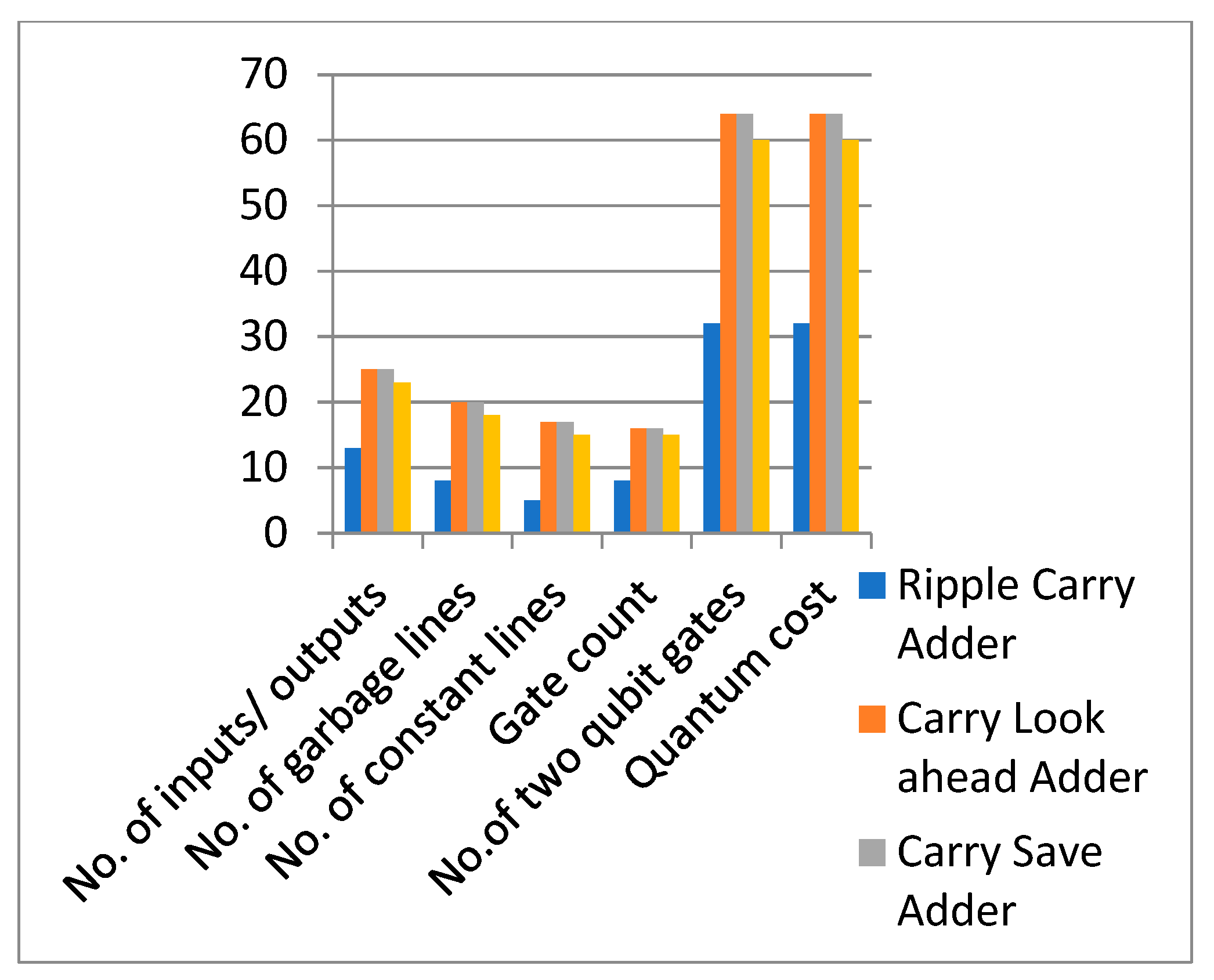
Figure 29.
Performance analysis of Different Multiplier configurations. Where * indicates the partial product output and not the final product of two 4-bit numbers in all the references and hence the quantum cost of these [5,6] circuits will be finalized after adding further stages in these circuits and hence the quantum cost for final product of 4 bit multiplier using Ripple Carry adder and Carry Save adder is definitely greater than 140 and 144 which is the landmark for the proposed multiplier circuit. At least 10% to 48% reduction in the quantum cost is observed referring above table parameters in the proposed designs.
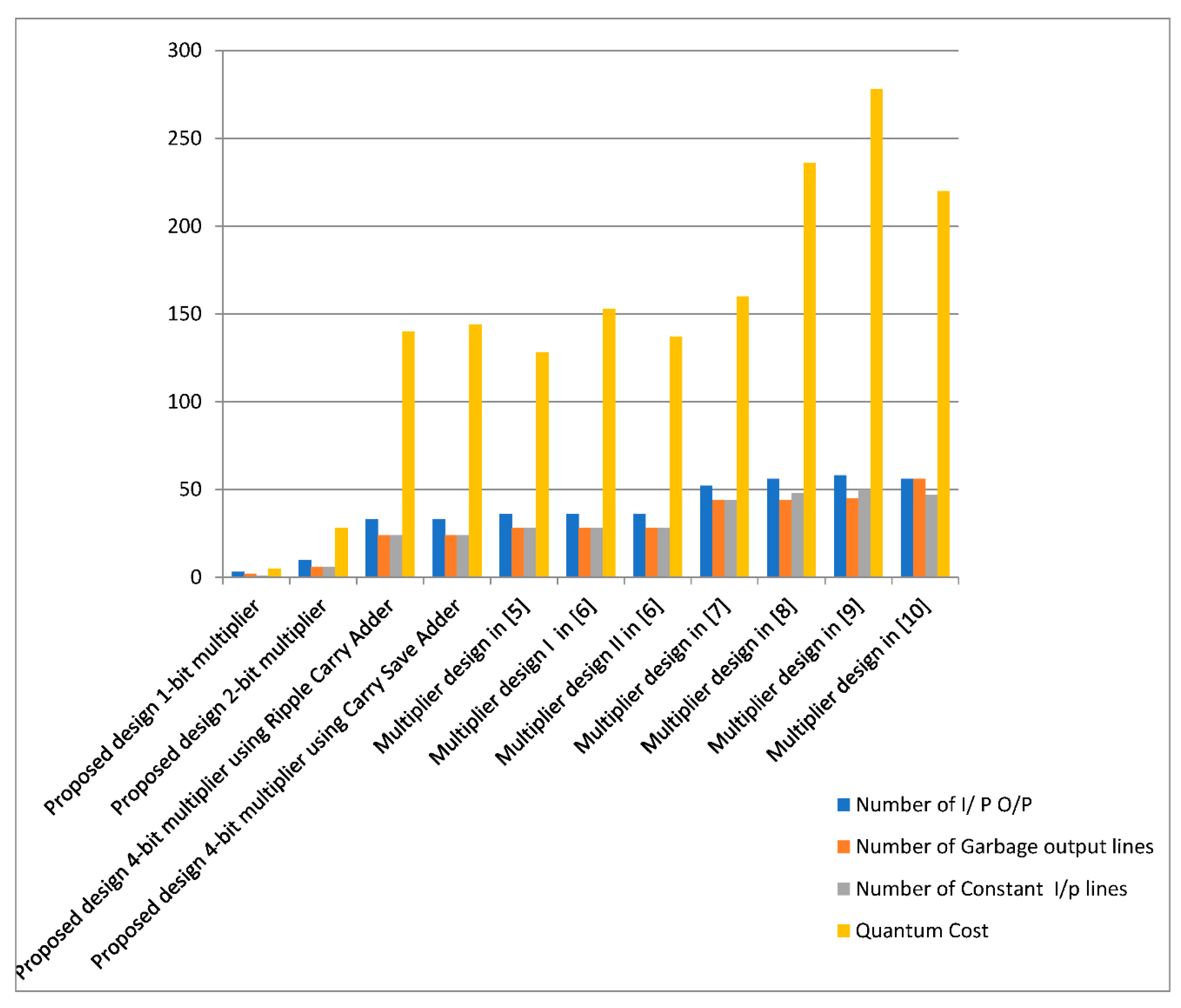
Figure 30.
Comparative analysis of Different Adders and Multiplier configurations.
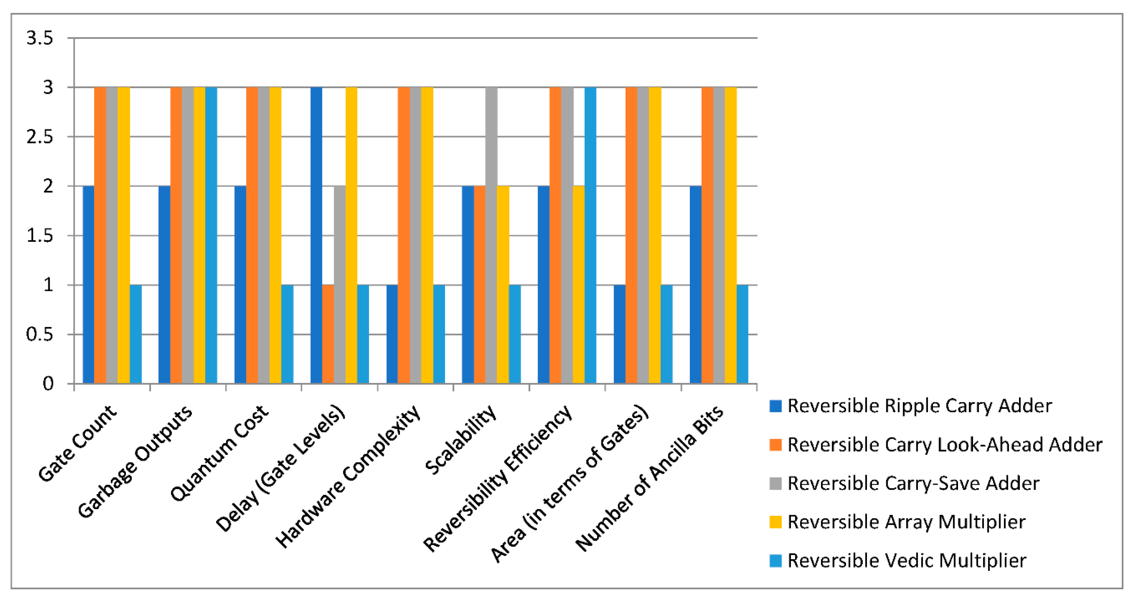

Table 1.
Truth table for Peres gate.
| Input Variables | Output Variables | ||||
|---|---|---|---|---|---|
| a | b | c | a | b | c |
| 0 | 0 | 0 | 0 | 0 | 0 |
| 0 | 0 | 1 | 0 | 0 | 1 |
| 0 | 1 | 0 | 0 | 1 | 0 |
| 0 | 1 | 1 | 0 | 1 | 1 |
| 1 | 0 | 0 | 1 | 1 | 0 |
| 1 | 0 | 1 | 1 | 1 | 1 |
| 1 | 1 | 0 | 1 | 0 | 1 |
| 1 | 1 | 1 | 1 | 0 | 0 |
Table 2.
Use of gates for Different MULTIPLIER configurations.
| Multiplier Circuit | No. Of Reversible Gates | |||
|---|---|---|---|---|
| Peres Gates | Toffoli Gates | Feynman Gates | Other Gates | |
| Proposed design 1-bit | 1 | - | - | - |
| Proposed design 2-bit | 2 | 4 | - | - |
| Proposed design 4-bit multiplier using RCA |
15 | 16 | - | - |
| Proposed design 4-bit multiplier using CSA | 16 | 16 | - | - |
| Multiplier design in [5] | 20 | - | - | 8 PFAG |
| Multiplier design I in [6] | 11 | 9 | - | 8 PFAG- |
| Multiplier design II in [6] | 11 | 9 | - | 8 HNG |
| Multiplier design in [7] | 20 | - | 16 | 8 PFAG- |
| Multiplier design in [8] | 16 | - | 16 | 12 MKG |
| Multiplier design in [9] | - | - | 16 | 16 FRG + 13 TSG |
| Multiplier design in [10] | - | 12 | 16 | 16 FRG + 12 NG |
Disclaimer/Publisher’s Note: The statements, opinions and data contained in all publications are solely those of the individual author(s) and contributor(s) and not of MDPI and/or the editor(s). MDPI and/or the editor(s) disclaim responsibility for any injury to people or property resulting from any ideas, methods, instructions or products referred to in the content. |
© 2024 by the authors. Licensee MDPI, Basel, Switzerland. This article is an open access article distributed under the terms and conditions of the Creative Commons Attribution (CC BY) license (http://creativecommons.org/licenses/by/4.0/).
Copyright: This open access article is published under a Creative Commons CC BY 4.0 license, which permit the free download, distribution, and reuse, provided that the author and preprint are cited in any reuse.


