Submitted:
21 August 2024
Posted:
21 August 2024
You are already at the latest version
Abstract
In this paper, we investigate various graphene monolayer nanomesh structures (diodes) formed only by nanoholes, with a diameter of just 20 nm and etched from the graphene layer in different shapes (such as rhombus, bow-tie, rectangle, trapezoid, and triangle), and their electrical properties targeting electromagnetic energy harvesting applications. In this respect, the main parameters characterizing any nonlinear device for energy harvesting are extracted from tens of measurements performed on a single chip containing the fabricated diodes. The best nano-perforated graphene structure is the triangle nanomesh one, which exhibits remarkable performance in terms of its characteristic parameters, i.e., a 420 Ω differential resistance for optimal impedance matching to an antenna, a high responsivity greater than 1000 V/W, and a low noise equivalent power of 847 pW/√Hz at 0 V.
Keywords:
diode
; electromagnetic radiation
; energy harvesting
; graphene
; quantum technologies.
1. Introduction
Graphene monolayers, which are single sheets of carbon atoms organized in a honeycomb lattice, show an impressive electrical performance, such as high mobility or ballistic transport at room temperature with a mean-free-path of hundreds of nanometers, but has no bandgap [1]. When a graphene monolayer is perforated with an array of holes termed as antidots [2] or nanomeshes, a bandgap of 200-300 meV is opened in graphene [3,4,5].
In the case of field-effect transistors (FETs) whose channel is a graphene monolayer perforated with nanoholes (with a diameter of 20 nm and a period of 100 nm), and with a channel width of 2 µm and different channel lengths between 1 and 8 µm, the mobility attains values from 10400 cm2/V∙s for a channel length of 1 µm to about 550 cm2/V∙s for a channel length of 8 µm. All these transistors have an on-off ratio of at least 103 at drain and gate voltage values less than 2 V. Therefore, changing the length of the nano-perforated graphene channel we are able to engineer the mobility of the carriers, thus making it similar to that of Si, GaAs, or InP [5].
The applications of nano-perforated graphene monolayers are found in many nanotechnology areas, such as biosensors [6], gas sensors [7], pressure sensors [8], and electronic skin [9]. In particular, nanomeshes have shown amazing results in low thermal conductivity [10] and thermoelectric applications [11]. Graphene nanomeshes are also used as transparent electrodes for solar cells [12]. Very recently, FETs possessing a graphene nanomesh channel have been used to harvest microwaves using the pyroelectric effect at room temperature [13] and at cryogenic temperatures [14]. There are important applications of the nano-perforated (or holey) graphene in batteries, supercapacitors, and other energy storage devices [15]. Hence, it is straightforward to investigate whether graphene nanomeshes can be used for electromagnetic energy harvesting applications.
The electromagnetic energy harvesting from microwaves to infrared radiation can be performed by an antenna with a nonlinear element (which could be an unbiased diode or transistor [16,17]) integrated between its two arms, termed as rectenna. The incoming electromagnetic radiation is transformed into a DC signal by the nonlinear device. We have to point out that the current-voltage dependence of the nonlinear element could not resemble a typical rectification diode, in which there is a region of very low current followed by a region where the current rapidly increases with two or three orders of magnitude. For example, a well-known nonlinear device suitable for electromagnetic energy harvesting from microwaves to infrared is the metal-insulator-metal (MIM) diode, i.e., a tunnelling diode where the current has an exponential dependence on voltage irrespective of the fact that the latter is either positive or negative [18].
In this work, we have fabricated at the wafer level and measured uniform shape (rectangle) and nonuniform-shape (triangle, trapezoid, rhombus, bow-tie) structures made of graphene monolayer, transferred on a 4-inch wafer of doped silicon/silicon dioxide (Si/SiO2), and formed exclusively by nano-holes (with a diameter of 20 nm). Then, we have extracted the performance parameters described above for evaluating the best geometry suitable for electromagnetic energy harvesting applications.
2. Key Performance Parameters of a Diode and Their Extraction from the Current-Voltage Characteristics
Regardless of the nonlinear device used in the rectenna, there are several performance parameters that can be extracted from the current-voltage characteristics and that characterize any device used in electromagnetic energy harvesting, such as diodes. These parameters are the following:
the differential resistance, defined as
the nonlinearity, defined as
the sensitivity, defined as
the responsivity, defined as
and the noise equivalent power, defined as
where RD0 = RD(V=0) is the differential resistance RD (in Ω) at 0 V. While the nonlinearity, the sensitivity, and the responsivity must be as high as possible, the differential resistance and the noise equivalent power must attain minimum values to ensure an efficient conversion of the electromagnetic energy into DC power. In fact, minimizing RD allows for the optimal impedance matching to an antenna, which is a prerequisite for the maximum power transfer to the nonlinear device. At the same time, it is desirable to have the NEP as low as possible, since a low NEP value corresponds to a lower noise floor, which entails a more sensitive harvester and lower noise characteristics in the output signal.
RD = 1⁄(∂I⁄∂V),
χ = (∂I⁄∂V)⁄(I⁄V),
γ = ((∂2I)⁄(∂V2))⁄(∂I⁄∂V),
β = 0.5 RD γ,
NEP=√(4 kB T RD0)⁄β,
3. Fabrication of the Graphene Nanomesh Structures at the Wafer Scale
The uniform and nonuniform graphene nanomesh devices were fabricated on a doped Si/SiO2 4-inch wafer. The thickness of the Si wafer is 525 µm and the SiO2 layer has a thickness of 300 nm. The SiO2 was grown by thermal oxidation. Further, the graphene monolayer was transferred on the Si/SiO2 substrate by Graphenea (Spain). The technological processes, as well as a review of the fabrication methods of the graphene nanomesh used by us, are given in detail elsewhere and will be only briefly explained here [15,19]. The Raman spectroscopy was used to map the graphene monolayer chip. We have observed that about 80% of wafer’s surface was covered with graphene monolayer, the rest being areas with graphene multilayers containing 4-6 monolayers and grain boundaries defects. The fabrication consists in the following steps: (i) patterning the graphene channel by electron-beam lithography (EBL) and reactive ion etching (RIE); (ii) patterning the shapes of the nanomesh geometries using EBL; (iii) patterning, metallization, and liftoff of the metallic contacts, i.e., Cr (5 nm)/Au (240 nm) deposited using an e-beam process (the chrome thin film being necessary as an adhesion layer for gold). In total, 100 graphene nanomesh devices were measured. In Figure 1, Figure 2, and Figure 3 we show the SEM images of the graphene nanomesh devices of different forms. In Figure 1a-b, the rhombus and bow-tie graphene nanomesh structures with their metallic contacts are displayed. In Figure 2a-c, we present more in detail several graphene monolayer nanomeshes in the shape of a rectangle (Figure 2a), a triangle (Figure 2b), and a trapezoid (Figure 2c, further termed as “delta”) without metal contacts. Finally, Figure 3 shows part of the fabricated wafer and details of the metallic contacts at an increasing degree of magnification.
4. Measurements and Discussion
The current-voltage measurements were made using a Keithley SCS 4200 equipment. All measurements were made at room temperature. The entire probe station for on-wafer characterization is located inside a Faraday cage and is connected to the equipment via low-noise amplifiers. All the 100 devices were measured and 90 of them worked with a remarkable reproducibility, since the current measurements at the same voltage of the same kind of graphene nanomesh structures exhibit variances of less than 3%.
We have extracted the performance parameters using equations (1)-(5) described above, i.e., the differential resistance RD (Ω), the nonlinearity χ (a.u.), the sensitivity γ (V-1), the voltage responsivity β (V/W), and the noise equivalent power NEP (pW/√Hz), all of them in the voltage range between -1 and 1 V. We present these parameters for all the types of graphene nanomesh structures fabricated as follows: rhombus, bow-tie, rectangle (two versions of it, i.e., with a distance between the nano-holes of 70 nm and 100 nm, respectively), triangle, and delta.
Figure 4 depicts the performance of the nanomesh bow-tie graphene structures. The DC current is quite high and attains values between approximately -0.81 and 0.86 mA, with a minimum RD of 0.77 kΩ at 0 V and a maximum χ = 1 at 0.02 V. The sensitivity spans the range between -4 and 4 V-1 (0.06 V-1 at 0 V), with an excellent responsivity between -5×10³ and 5×10³ V/W (24 V/W at 0 V), whereas the maximum NEP is 1900 pW/√Hz at -0.14 V and NEP = 150 pW/√Hz at 0 V. We note here that a negative voltage responsivity is associated to an n-type behavior, whereas a p-type behavior generates a positive voltage responsivity [20]. From Figure 4, it is apparent that this device is an excellent candidate for zero-bias detection/energy harvesting, also thanks to acceptable value of its differential resistance (which can reach several kΩ for graphene geometric diodes, thus making almost impossible the design of a matching network for maximum power transfer).
The performance of the diodes having the shape of a rhombus (Figure 5) is similar to that of the graphene nanomesh structures having the shape of a bow-tie in terms of current level, RD (0.79 kΩ at 0 V), nonlinearity, and responsivity (in this case, the minimum is about -1×10⁴ and β = -9 V/W at 0 V), but the maximum NEP is substantially lower (457 pW/√Hz at 0.44 V). However, NEP = 398 pW/√Hz at 0 V and on average the NEP is higher than that of the bow-tie graphene nanomesh structures.
The graphene nanomesh structure with the trapezoid shape and termed as “delta” (Figure 6) shows RD = 0.55 kΩ at 0 V, with similar values for the nonlinearity with the rhombus graphene nanomesh structures, a slightly higher sensitivity (-0.05 V-1 at 0 V), a responsivity with the maximum around 2.5×10³ V/W (-14.25 V/W at 0 V), and a low NEP (the maximum is 365 pW/√Hz at -0.06 V). Hence, this delta-shaped diode guarantees an even easier impedance matching in low-power high-frequency applications working at voltage values near 0 V, as well as a very low NEP.
If we now consider the two rectangle-shaped diodes termed as “rectangle#1” and “rectangle#2” (Figure 7 and Figure 8, respectively), one can notice the much lower current values (between -300 and 300 µA). Consequently, RD is also higher at 0 V: 2.5 kΩ for diode “rectangle#1” and 1.92 kΩ for diode “rectangle#2”. However, the nonlinearity is the highest among all the fabricated diodes: 1.15 at 0.02 V for diode “rectangle#1” and 1.09 at 0.02 V for diode “rectangle#2”, together with a higher sensitivity between -10 and 10 V-1. The responsivity is also higher, i.e., in the range -3×10⁴ – 2×10⁴ for diode “rectangle#1” and in the range -1×10⁴ – 1×10⁴ for diode “rectangle#2”. The NEP is particularly low for diode “rectangle#1” and does not exceed 206 pW/√Hz at -0.1 V, while for diode “rectangle#2” the behavior is quite homogeneous despite the peak of 431 pW/√Hz at -0.12 V. Hence, these two diodes are suitable for low-power and low-noise applications requiring a high sensitivity and a high responsivity, at the cost of some matching issues.
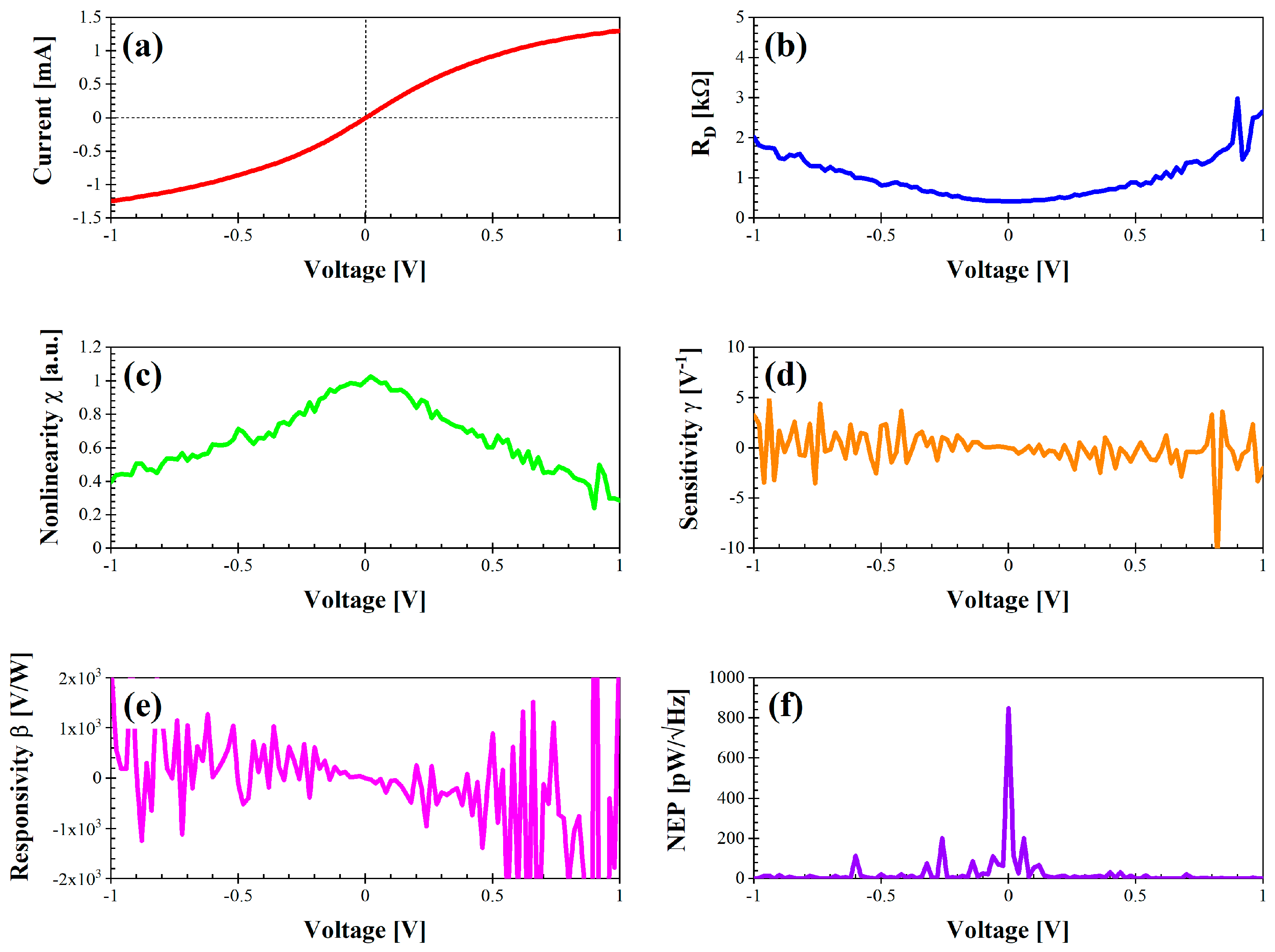
Finally, we report here the performance of the graphene nanomesh structure having the shape of a triangle (Figure 9). At a first glance, its parameters resemble those obtained for bow-tie and rhombus, but the DC current is the highest (between -1.24 and 1.30 mA) and RD is the lowest (i.e., 0.42 kΩ at 0 V), thus making it the most suitable for integration with an antenna. Nonlinearity, sensitivity, and responsivity are similar with bow-tie and rhombus graphene nanomesh structures. Last, the NEP has a peak of 847 pW/√Hz at 0 V but it attains quite low values over the whole voltage range.
The question that immediately arises is: which is the best structure for electromagnetic energy harvesting? The triangle-shaped graphene nanomesh structure is the best one, because it exhibits the lowest RD of only 420 Ω, meaning that it can be easily matched to an antenna like a bow-tie, which has an input impedance in the range 200-300 Ω. This result is extremely significant and solves a quite important conundrum, if one considers that the impedance matching to an antenna is a major issue for electromagnetic energy harvesting, since it hinders the maximum power transfer to the rectifying diode. With this type of structures, we are far from the performance of uniform graphene monolayers with a microwave impedance around 2-3 kΩ, this aspect being the main reason why graphene antennas have very low radiation efficiency values in microwaves and millimeter-waves. Moreover, if we compare ours results with similar ones obtained for various types nonlinear devices dedicated for electromagnetic energy harvesting in microwaves (and shown in Table III and IV in [21]), we see that by far the proposed graphene monolayer nanomesh structures are among the best fabricated and measured up to now, especially regarding the differential resistance, i.e., the most critical parameter for matching a nonlinear device to an antenna.
Why? It is notorious that the graphene/metal contact resistance is high due to the lack of a bandgap in graphene monolayers; nevertheless, there are numerous methods to reduce it as it is reported in many review papers [22,23]. Thus, the solution is to open a bandgap in graphene to reduce the contact resistance. The quantum-confined structures like graphene nanoribbons and quantum dots or antidots, i.e., nanomeshes, allow opening a bandgap in graphene, hence drastically reducing the metal-graphene resistance [22]. In fact, nanomesh structures can be classified as a type of semiconducting graphene that facilitates the alignment of the Fermi levels between the metal of the contact and graphene itself. This can be seen from any RD(V) dependence, which can be easily approximated as a linear one.
Finally, we have shown in [13] that a FET having a graphene monolayer channel with length Lch = 2500 nm and width Wch = 2000 nm, perforated with holes with a diameter of 30 nm and a distance of 100 nm along the horizontal and vertical axes (hence, a very large nanomesh rectangle, much larger than what has been presented here), is able to work as microwave detector/harvester up to 10 GHz at room temperature. The graphene nanomesh structures of this work possess a length that is at least three-four times smaller, whereas the width is two times smaller. For this reason, we can expect that these devices could work as harvesters at frequencies as high as 40 GHz or even more. All these nano-perforated devices are a part of the so-called graphene nanoporous materials, with excellent absorbing properties at microwaves and at infrared frequencies [3].
5. Conclusions
In this paper, we have fabricated at the wafer level and measured tens of graphene nanomesh structures and investigated if these structures are feasible for electromagnetic energy harvesting. The main finding is that a large part of these nano-patterned diodes exhibits excellent properties for harvesting the electromagnetic radiation. We stress here that these nano-perforated structures are a part of the so-called graphene nanoporous materials, with excellent absorbing properties at microwaves and at infrared frequencies. This makes the proposed graphene nanomesh structures ideal candidates as nonlinear devices to be integrated in harvesters at different wavelengths, a subject that will be further investigated in a forthcoming paper.
Author Contributions
Conceptualization, M.D., D.D., and A.D.; methodology, M.D., D.D., and A.D.; software, M.A.; validation, M.D. and A.D.; formal analysis, M.A.; investigation, M.D.; resources, A.D.; data curation, M.D. and M.A.; writing—original draft preparation, M.D.; writing—review and editing, M.A.; visualization, M.A.; supervision, M.D.; project administration, M.D.; funding acquisition, M.A. and M.D. All authors have read and agreed to the published version of the manuscript.
Funding
This research was partially funded by the European Project Horizon Europe HORIZON-EIC-2022-TRANSITIONCHALLENGES-01 “SMARTWAY”, under Grant No. 101103057, by the European Project Horizon Europe HORIZON-EIC-2023-PATHFINDERCHALLENGES-01 “POWERSAT”, under Grant No. 101162320, and by the Romanian Ministry of Research, Innovation and Digitization: in part by CCCDI—UEFISCDI, under Project PN-III-P4-PCE-2021-0223 within PNCDI III, under Project PN-IV-P8-8.1-PRE-HE-ORG-2023-0033 within PNCDI IV, and in part by the Core Program within the National Research Development and Innovation Plan 2022-2027, under Project 2307.
Data Availability Statement
The original contributions presented in the study are included in the article, further inquiries can be directed to the corresponding author.
Conflicts of Interest
The authors declare no conflicts of interest. The funders had no role in the design of the study; in the collection, analyses, or interpretation of data; in the writing of the manuscript; or in the decision to publish the results.
References
- Dragoman, M.; Dragoman, D. Atomic-Scale Electronics Beyond CMOS; Springer International Publishing: Cham, 2021; ISBN 978-3-030-60562-9. [Google Scholar]
- Sandner, A.; Preis, T.; Schell, C.; Giudici, P.; Watanabe, K.; Taniguchi, T.; Weiss, D.; Eroms, J. Ballistic Transport in Graphene Antidot Lattices. Nano Lett 2015, 15, 8402–8406. [Google Scholar] [CrossRef]
- Yang, J.; Ma, M.; Li, L.; Zhang, Y.; Huang, W.; Dong, X. Graphene Nanomesh: New Versatile Materials. Nanoscale 2014, 6, 13301–13313. [Google Scholar] [CrossRef] [PubMed]
- Bai, J.; Zhong, X.; Jiang, S.; Huang, Y.; Duan, X. Graphene Nanomesh. Nat Nanotechnol 2010, 5, 190–194. [Google Scholar] [CrossRef]
- Dragoman, M.; Dinescu, A.; Dragoman, D. Solving the Graphene Electronics Conundrum: High Mobility and High on-off Ratio in Graphene Nanopatterned Transistors. Physica E Low Dimens Syst Nanostruct 2018, 97, 296–301. [Google Scholar] [CrossRef]
- Yang, Y.; Yang, X.; Zou, X.; Wu, S.; Wan, D.; Cao, A.; Liao, L.; Yuan, Q.; Duan, X. Ultrafine Graphene Nanomesh with Large On/Off Ratio for High-Performance Flexible Biosensors. Adv Funct Mater 2017, 27. [Google Scholar] [CrossRef]
- Paul, R.K.; Badhulika, S.; Saucedo, N.M.; Mulchandani, A. Graphene Nanomesh As Highly Sensitive Chemiresistor Gas Sensor. Anal Chem 2012, 84, 8171–8178. [Google Scholar] [CrossRef]
- Qiao, Y.; Jian, J.; Tang, H.; Ji, S.; Liu, Y.; Liu, H.; Li, Y.; Li, X.; Han, F.; Liu, Z.; et al. An Intelligent Nanomesh-Reinforced Graphene Pressure Sensor with an Ultra Large Linear Range. J Mater Chem A Mater 2022, 10, 4858–4869. [Google Scholar] [CrossRef]
- Qiao, Y.; Li, X.; Wang, J.; Ji, S.; Hirtz, T.; Tian, H.; Jian, J.; Cui, T.; Dong, Y.; Xu, X.; et al. Intelligent and Multifunctional Graphene Nanomesh Electronic Skin with High Comfort. Small 2022, 18. [Google Scholar] [CrossRef] [PubMed]
- Feng, T.; Ruan, X. Ultra-Low Thermal Conductivity in Graphene Nanomesh. Carbon N Y 2016, 101, 107–113. [Google Scholar] [CrossRef]
- Li, D.; Gong, Y.; Chen, Y.; Lin, J.; Khan, Q.; Zhang, Y.; Li, Y.; Zhang, H.; Xie, H. Recent Progress of Two-Dimensional Thermoelectric Materials. Nanomicro Lett 2020, 12, 36. [Google Scholar] [CrossRef]
- Shin, D.H.; Kim, J.H.; Jung, D.H.; Choi, S.-H. Graphene-Nanomesh Transparent Conductive Electrode/Porous-Si Schottky-Junction Solar Cells. J Alloys Compd 2019, 803, 958–963. [Google Scholar] [CrossRef]
- Dragoman, M.; Aldrigo, M.; Dinescu, A.; Vasilache, D.; Iordanescu, S.; Dragoman, D.; Laudadio, E.; Pavoni, E. Harvesting Microwave Energy Using Pyroelectricity of Nanostructured Graphene/Zirconium-Doped Hafnium Oxide Ferroelectric Heterostructures. Nanotechnology 2023, 34, 205202. [Google Scholar] [CrossRef]
- Aldrigo, M.; Dragoman, M.; Dinescu, A.; Vasilache, D.; Iordanescu, S.; Dinu, L.A.; Dragoman, D.; Laudadio, E.; Pavoni, E.; Pierantoni, L.; et al. Demonstration of Microwave Harvesting Through Pyroelectricity in Cryogenic Conditions: A Quantum-to-Experimental Approach. IEEE Microwave and Wireless Technology Letters 2024, 34, 853–856. [Google Scholar] [CrossRef]
- Wang, D.; Dou, Y.; Zhang, X.; Bi, K.; Panneerselvam, I.R.; Sun, H.; Jiang, X.; Dai, R.; Song, K.; Zhuang, H.; et al. Manufacturing and Applications of Multi-Functional Holey Two-Dimensional Nanomaterials – A Review. Nano Today 2024, 55, 102162. [Google Scholar] [CrossRef]
- Costanzo, A.; Dionigi, M.; Masotti, D.; Mongiardo, M.; Monti, G.; Tarricone, L.; Sorrentino, R. Electromagnetic Energy Harvesting and Wireless Power Transmission: A Unified Approach. Proceedings of the IEEE 2014, 102, 1692–1711. [Google Scholar] [CrossRef]
- Rectenna Solar Cells; Springer New York: New York, NY, 2013; ISBN 978-1-4614-3715-4.
- Shriwastava, S.; Tripathi, C.C. Metal–Insulator–Metal Diodes: A Potential High Frequency Rectifier for Rectenna Application. J Electron Mater 2019, 48, 2635–2652. [Google Scholar] [CrossRef]
- Dragoman, M.; Dinescu, A.; Dragoman, D. Room Temperature Nanostructured Graphene Transistor with High on/off Ratio. Nanotechnology 2017, 28, 015201. [Google Scholar] [CrossRef] [PubMed]
- Westlund, A.; Winters, M.; Ivanov, I.G.; Hassan, J.; Nilsson, P.-Å.; Janzén, E.; Rorsman, N.; Grahn, J. Graphene Self-Switching Diodes as Zero-Bias Microwave Detectors. Appl Phys Lett 2015, 106. [Google Scholar] [CrossRef]
- Cheraghi Bidsorkhi, H.; D’Aloia, A.G.; Tamburrano, A.; De Bellis, G.; Delfini, A.; Ballirano, P.; Sarto, M.S. 3D Porous Graphene Based Aerogel for Electromagnetic Applications. Sci Rep 2019, 9, 15719. [Google Scholar] [CrossRef]
- Watanabe, E.; Conwill, A.; Tsuya, D.; Koide, Y. Low Contact Resistance Metals for Graphene Based Devices. Diam Relat Mater 2012, 24, 171–174. [Google Scholar] [CrossRef]
- Giubileo, F.; Di Bartolomeo, A. The Role of Contact Resistance in Graphene Field-Effect Devices. Prog Surf Sci 2017, 92, 143–175. [Google Scholar] [CrossRef]
Figure 1.
Graphene monolayer nanomesh structures with metallic contacts: (a) rhombus and (b) bow-tie.
Figure 1.
Graphene monolayer nanomesh structures with metallic contacts: (a) rhombus and (b) bow-tie.
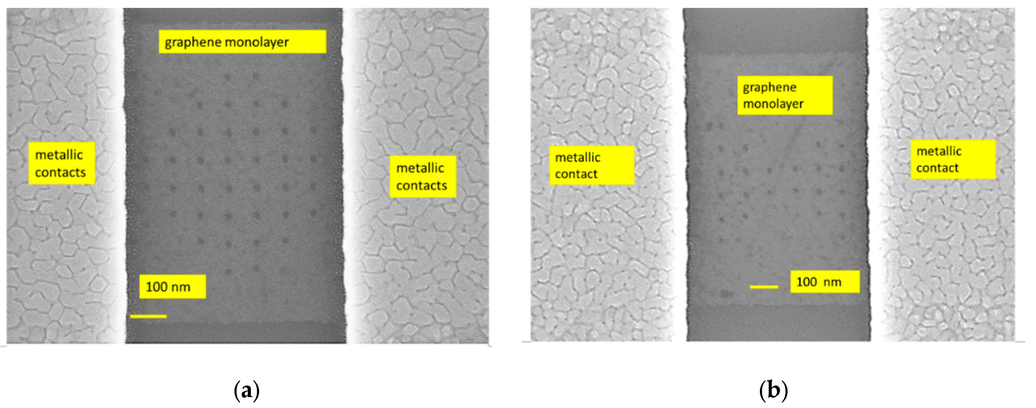
Figure 2.
Details of the graphene monolayer nanomeshes of different shapes: (a) rectangle, (b) triangle, and (c) delta.
Figure 2.
Details of the graphene monolayer nanomeshes of different shapes: (a) rectangle, (b) triangle, and (c) delta.
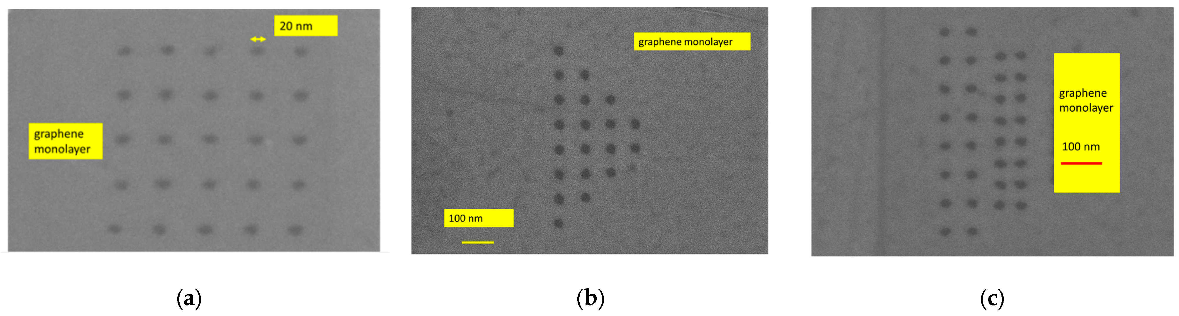
Figure 3.
A part of the graphene nanomesh chip with metallized electrodes and its details.
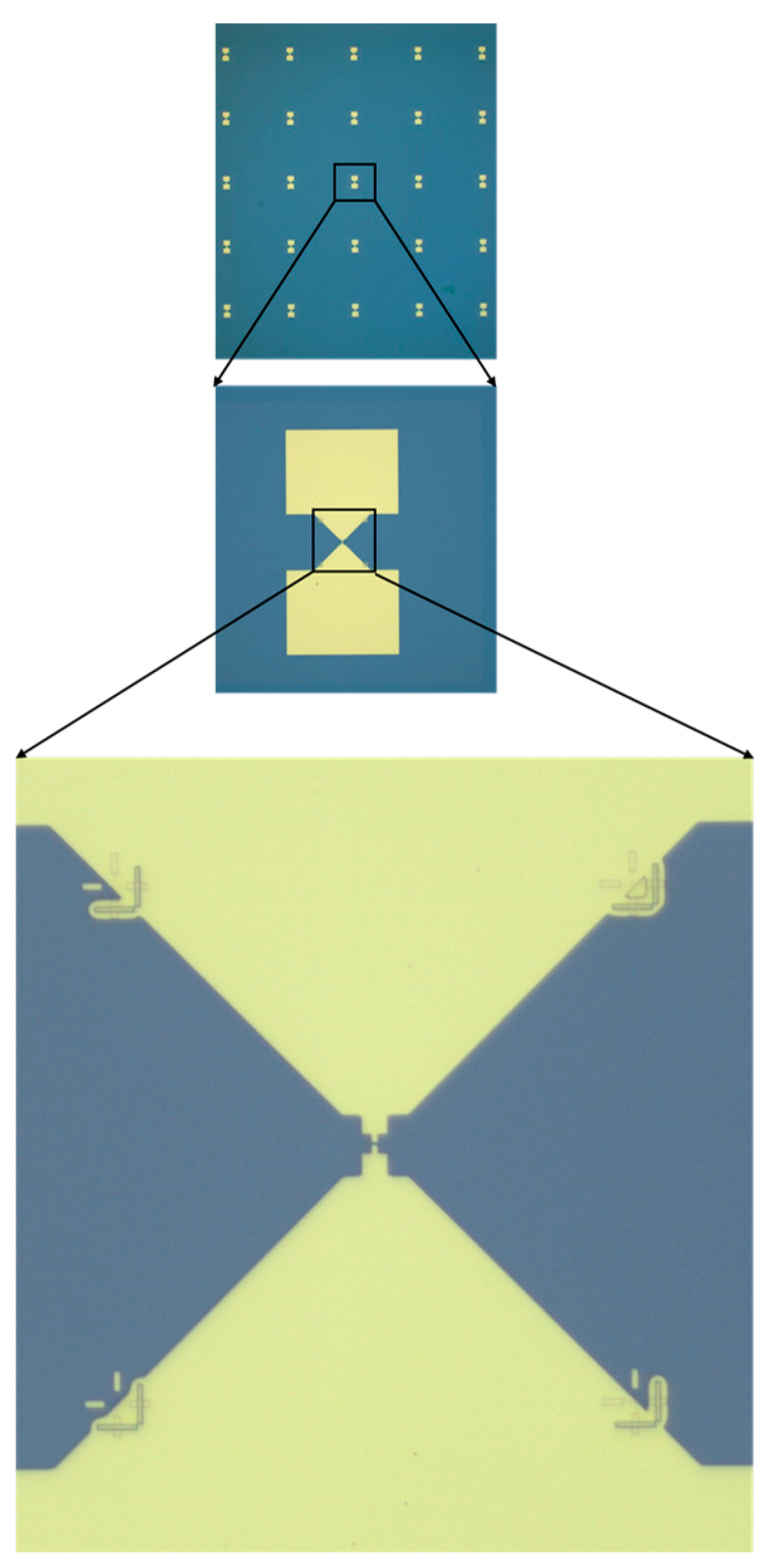
Figure 4.
Performance of the diode “bow-tie” in dark conditions: (a) I-V characteristics; (b) differential resistance RD (kΩ); (c) nonlinearity χ (a.u.); (d) sensitivity γ (V-1); (e) voltage responsivity β (V/W); (f) noise equivalent power (pW/√Hz).
Figure 4.
Performance of the diode “bow-tie” in dark conditions: (a) I-V characteristics; (b) differential resistance RD (kΩ); (c) nonlinearity χ (a.u.); (d) sensitivity γ (V-1); (e) voltage responsivity β (V/W); (f) noise equivalent power (pW/√Hz).
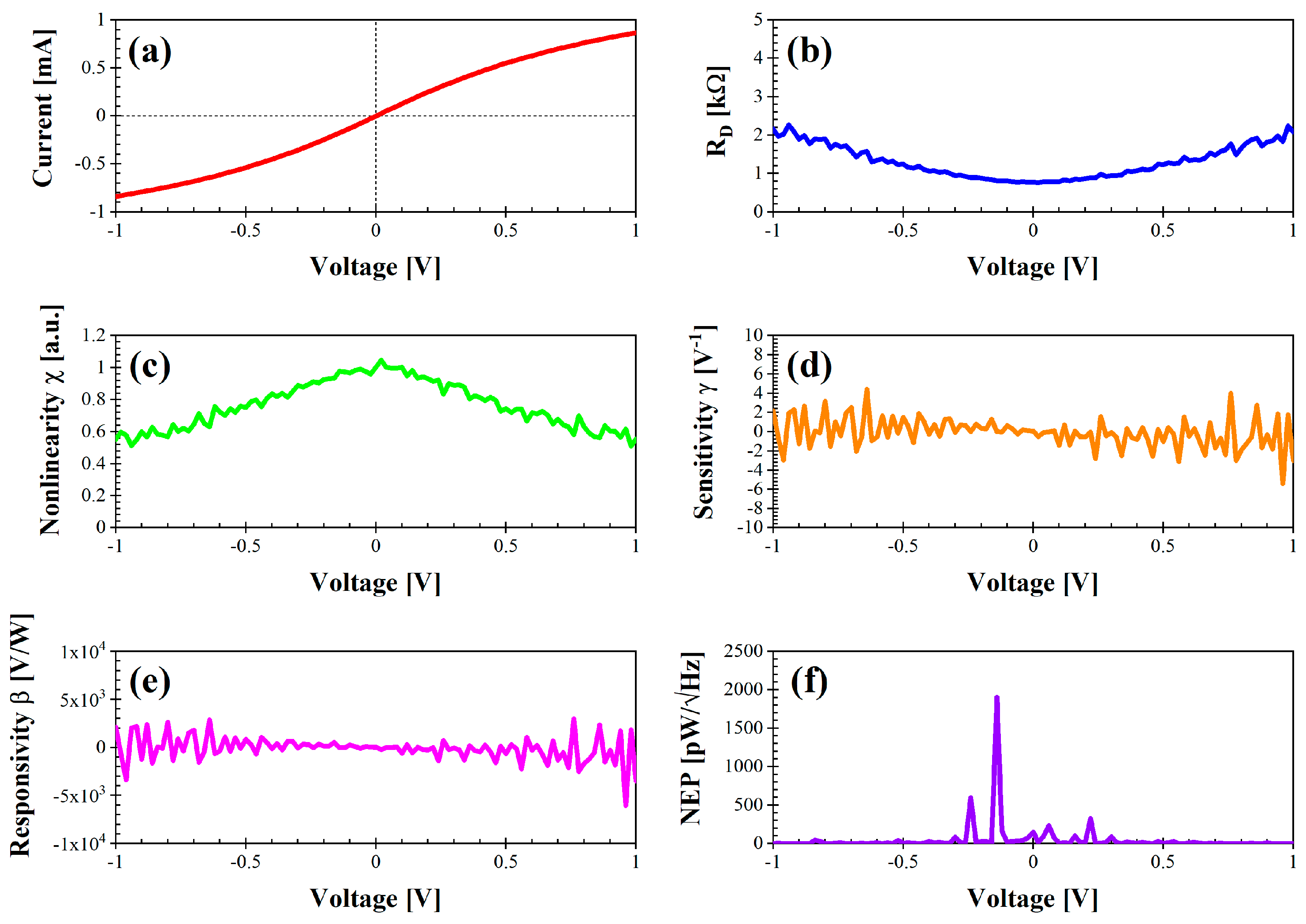
Figure 5.
Performance of the diode “rhombus” in dark conditions: (a) I-V characteristics; (b) differential resistance RD (kΩ); (c) nonlinearity χ (a.u.); (d) sensitivity γ (V-1); (e) voltage responsivity β (V/W); (f) noise equivalent power (pW/√Hz).
Figure 5.
Performance of the diode “rhombus” in dark conditions: (a) I-V characteristics; (b) differential resistance RD (kΩ); (c) nonlinearity χ (a.u.); (d) sensitivity γ (V-1); (e) voltage responsivity β (V/W); (f) noise equivalent power (pW/√Hz).
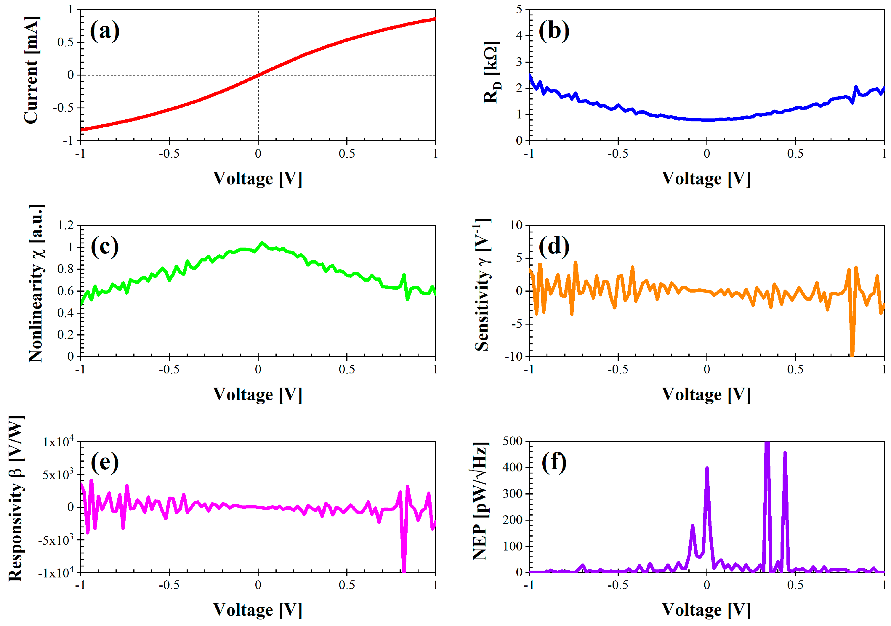
Figure 6.
Performance of the diode “delta” in dark conditions: (a) I-V characteristics; (b) differential resistance RD (kΩ); (c) nonlinearity χ (a.u.); (d) sensitivity γ (V-1); (e) voltage responsivity β (V/W); (f) noise equivalent power (pW/√Hz).
Figure 6.
Performance of the diode “delta” in dark conditions: (a) I-V characteristics; (b) differential resistance RD (kΩ); (c) nonlinearity χ (a.u.); (d) sensitivity γ (V-1); (e) voltage responsivity β (V/W); (f) noise equivalent power (pW/√Hz).
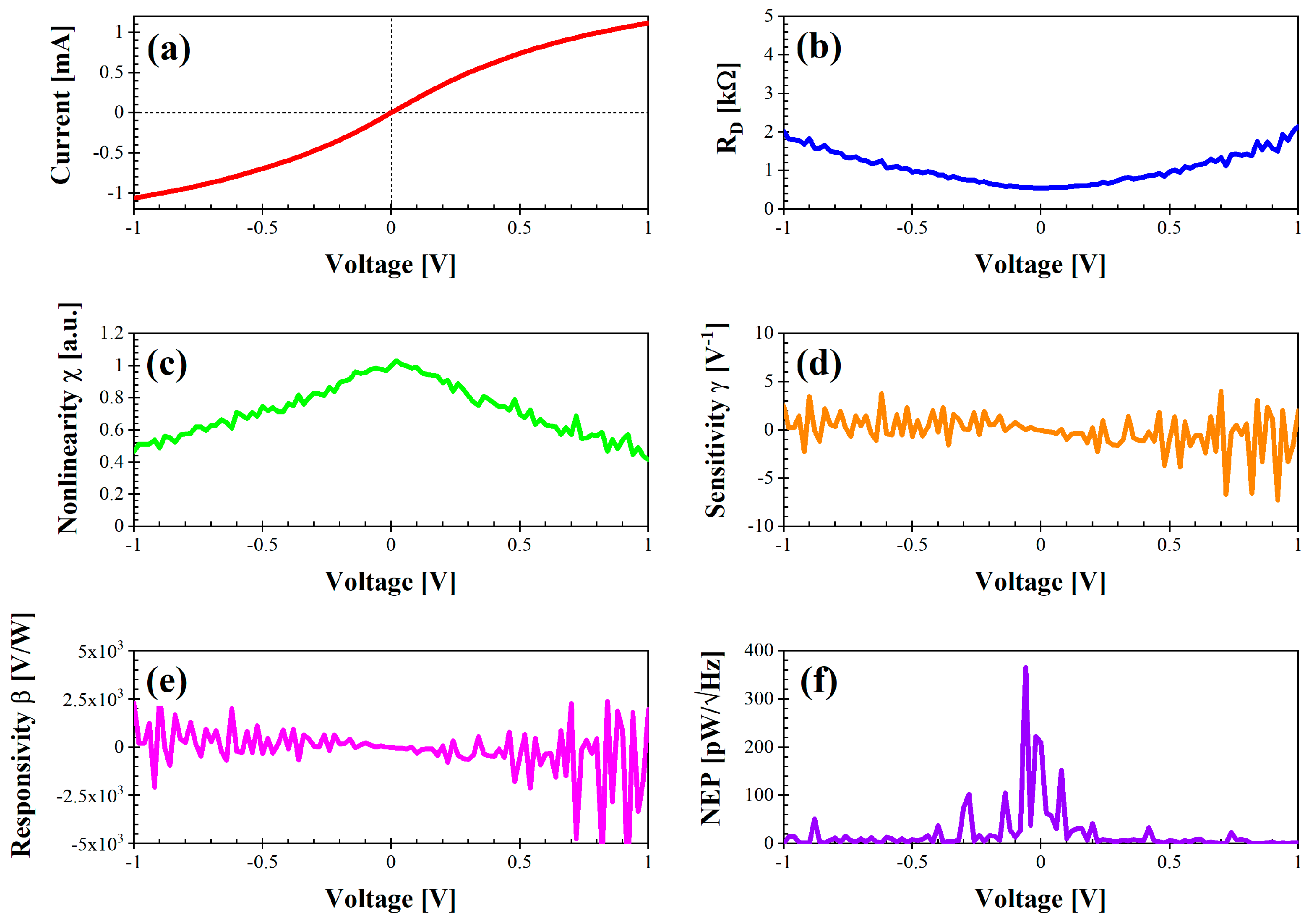
Figure 7.
Performance of the diode “rectangle#1” in dark conditions: (a) I-V characteristics; (b) differential resistance RD (kΩ); (c) nonlinearity χ (a.u.); (d) sensitivity γ (V-1); (e) voltage responsivity β (V/W); (f) noise equivalent power (pW/√Hz).
Figure 7.
Performance of the diode “rectangle#1” in dark conditions: (a) I-V characteristics; (b) differential resistance RD (kΩ); (c) nonlinearity χ (a.u.); (d) sensitivity γ (V-1); (e) voltage responsivity β (V/W); (f) noise equivalent power (pW/√Hz).
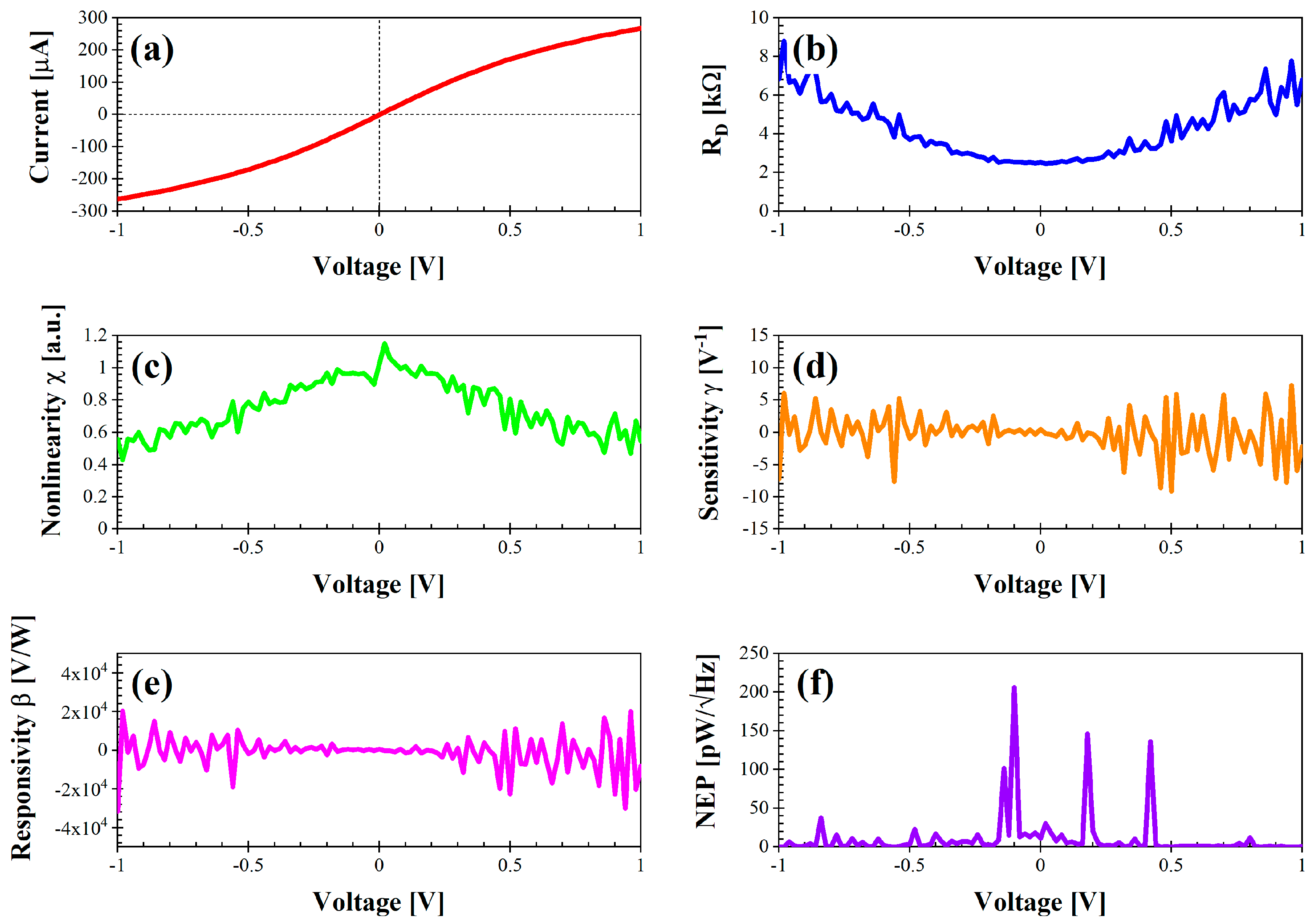
Figure 8.
Performance of the diode “rectangle#2” in dark conditions: (a) I-V characteristics; (b) differential resistance RD (kΩ); (c) nonlinearity χ (a.u.); (d) sensitivity γ (V-1); (e) voltage responsivity β (V/W); (f) noise equivalent power (pW/√Hz).
Figure 8.
Performance of the diode “rectangle#2” in dark conditions: (a) I-V characteristics; (b) differential resistance RD (kΩ); (c) nonlinearity χ (a.u.); (d) sensitivity γ (V-1); (e) voltage responsivity β (V/W); (f) noise equivalent power (pW/√Hz).
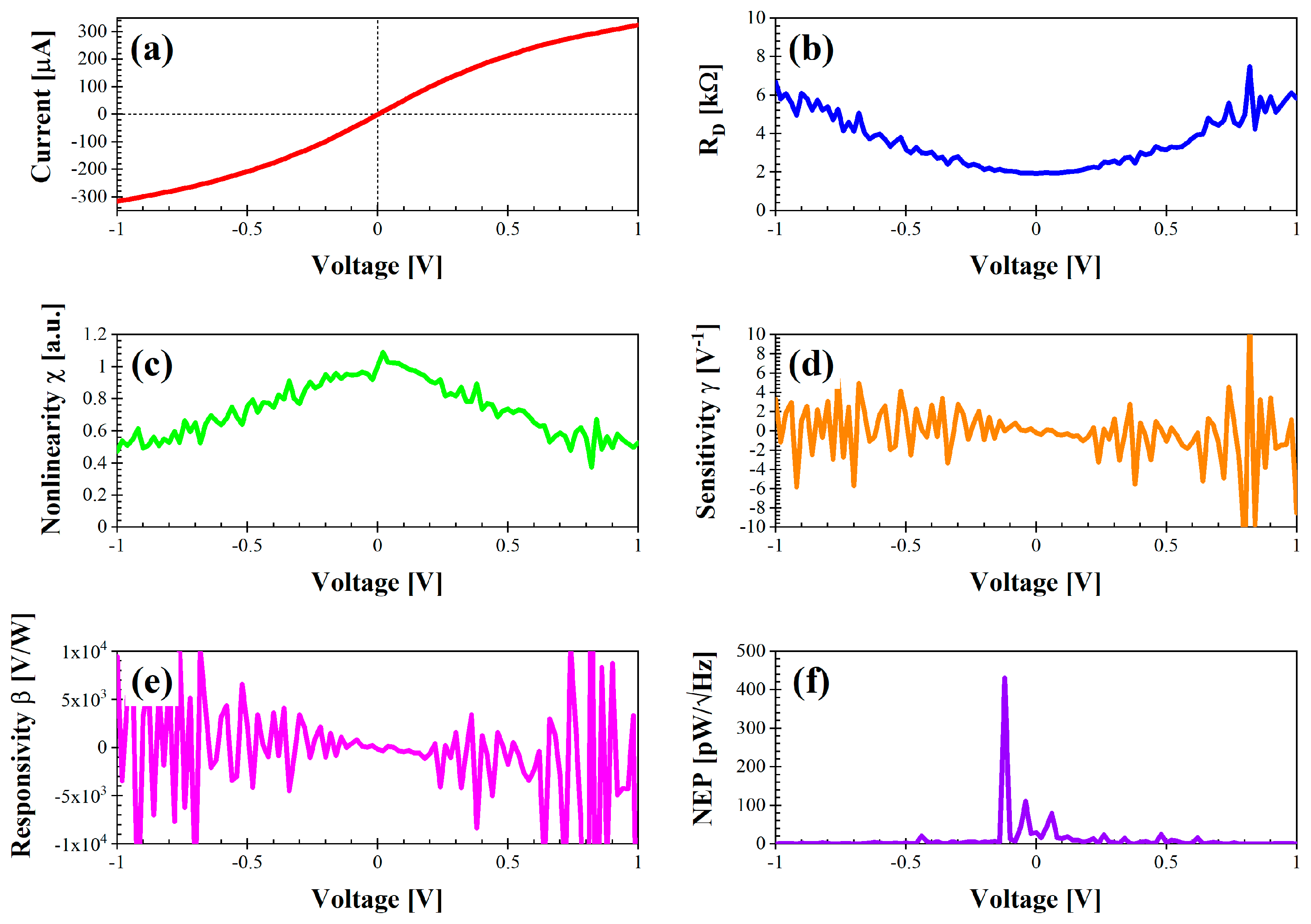
Figure 9.
Performance of the diode “triangle” in dark conditions: (a) I-V characteristics; (b) differential resistance RD (kΩ); (c) nonlinearity χ (a.u.); (d) sensitivity γ (V-1); (e) voltage responsivity β (V/W); (f) noise equivalent power (pW/√Hz).
Figure 9.
Performance of the diode “triangle” in dark conditions: (a) I-V characteristics; (b) differential resistance RD (kΩ); (c) nonlinearity χ (a.u.); (d) sensitivity γ (V-1); (e) voltage responsivity β (V/W); (f) noise equivalent power (pW/√Hz).
Disclaimer/Publisher’s Note: The statements, opinions and data contained in all publications are solely those of the individual author(s) and contributor(s) and not of MDPI and/or the editor(s). MDPI and/or the editor(s) disclaim responsibility for any injury to people or property resulting from any ideas, methods, instructions or products referred to in the content. |
© 2024 by the authors. Licensee MDPI, Basel, Switzerland. This article is an open access article distributed under the terms and conditions of the Creative Commons Attribution (CC BY) license (http://creativecommons.org/licenses/by/4.0/).
Copyright: This open access article is published under a Creative Commons CC BY 4.0 license, which permit the free download, distribution, and reuse, provided that the author and preprint are cited in any reuse.


