Submitted:
13 August 2024
Posted:
14 August 2024
You are already at the latest version
Abstract
Research in renewable energy sources and micro-grid systems is critical for the evolving power industry. Micro-grids can supply diverse loads while reducing dependency on the utility grid. This paper models both pico-grids and nano-grids in the Singapore Institute of Technology Punggol campus, incorporating solar PV, energy storage systems (ESS), power electronics converters, and both DC and AC loads, along with utility grid connections. The pico-grid includes a battery storage system, a single-phase inverter linked to a single-phase grid, and DC and AC loads. The nano-grid comprises solar PV panels, a boost converter, a battery storage system, a three-phase inverter connected to a three-phase grid, and AC loads. Both the pico-grid and nano-grid are configurable in standalone or grid-connected modes. This configuration flexibility allows for detailed operational analysis under various conditions. The study conducts subsystem-level modeling before integrating all components into the simulation environment. MATLAB/Simulink is utilized to model, simulate, and analyze the power flow in both the pico-grid and nano-grid under different operating conditions.
Keywords:
Pico-grid
; nano-grid
; microgrid
; distributed generation
; modeling
; simulation
1. Introduction
The global shift towards a clean energy environment has significantly driven the studies of renewable energy sources (RES). These sources are heralded for their environmental friendliness due to their minimal or zero emissions compared to traditional fossil fuels, which are major contributors to carbon dioxide emissions, greenhouse gases, and overall environmental pollution [1]. As a response to these environmental challenges, there has been a substantial move towards RES like hydroelectric, biomass, wind, solar, wave, tidal, and geothermal energy, which are continually replenished by nature [2].
Integration of RES within smart grid technology is a crucial development, bridging the gap between energy demand and supply. Smart grids, equipped with advanced metering systems (AMS), energy management systems (EMS), and advanced communication systems, manage the distribution and optimization of renewable energy more effectively than conventional grids. They handle challenges in supply-demand balance, power generation, distribution, and electricity pricing more adeptly [3,4].
This paper focuses on the modeling of nano-grids and pico-grids, which are essential components of the smart grid infrastructure. The nano-grid, suitable for individual buildings, and the pico-grid, designed for standalone applications within a building, aim to demonstrate how integration of solar photovoltaic (PV) systems and energy storage can optimize power flow and enhance grid reliability. The smaller power networks, picogrids and nanogrids, should be able to function both in an islanded (stand-alone) and a grid-connected mode and be able to operate steadily in a cluster [5]. In [6], a comprehensive review of the recent developments in nano-grid research, including the control topologies and methods that allow for the nano-grid’s intelligent control are covered. Operation of a basic nano-grid with rules-based controller and load behavior in response to fluctuating renewable energy source electricity availability is modelled in [7]. Open Energy Systems (OESs) concept and architecture for higher-level control of the components of a standalone nanogrid is introduced in [8]. In [9], use of optimal energy management system to mitigate the impact of energy uncertainties in an interconnection between microgrid nano-grid were studied. The power management of nano-grid for grid support and deploying power converters to regulate power quality is discussed in [10]. Recent research and development efforts in nano-grids are also focusing on ability to interconnect nano-grids to trade energy [11,12]. A decentralized blockchain mechanisms for demand response program in nano-grids is proposed in [13]. A predictive optimization-based model for optimal energy sharing plan between a cluster of nano-grids is proposed in [14].
With the establishment of the Singapore Institute of Technology (SIT) in Punggol Digital District, a Multi-Energy Micro-grid (MEMG) has been implemented and will be fully operational in late 2024, aiming to achieve zero emissions [15]. Approximately 10,000 m2 of solar panels will be installed on rooftops to power the campus, significantly reducing reliance on the main utility grid and advancing the institution’s sustainability goals. This development motivates the need for a testbed to model and analyze the operation of both pico-grids and nano-grids in the campus’s west zone.
This paper aims to model and simulate the pico-grid and nano-grid using MATLAB/Simulink to:
- i.
- Explore and study the individual subsystems of both the pico-grid and nano-grid.
- i.
- Model and integrate relevant components.
- i.
- Develop simulation models to analyze power flow.
- i.
- Perform tests to assess operations under realistic scenarios.
The primary contributions of this paper include the detailed study, modeling, and simulation of the pico-grid and nano-grid. This work constructs a comprehensive model of these systems using MATLAB/Simulink to facilitate power flow analysis under various operating conditions. In what follows, Section 2 discusses the proposed architecture for pico-grid and nano-grid and their modeling. Section 3 presents test conditions and simulation results. Section 4 concludes the paper and outlines future areas of work.
2. Systems Description and Modelling
2.1. Proposed Architecture of Pico-grid System
Figure 1 shows the proposed architecture of a pico-grid system to be implemented in various buildings at the SIT Punggol Campus. The building is a six-storey structure with two basement car parks and four levels of amenities, including classrooms, lecture theatres, and a server room. Each level is equipped with a standalone pico-grid system to supply power to DC and AC loads. Every two levels are connected via a circuit breaker to one phase of the utility grid, and each level’s pico-grid system includes a 1P+N circuit breaker for the option of islanded or grid-connected mode. For instance, levels B1 and B2 can be linked and connected to the single-phase grid by closing their respective circuit breakers, allowing load sharing if one level’s demand is higher.
The major components of the building are as follows:
- Levels 1 to 4 are designated for classrooms, lecture theatres, and a server room.
- Levels B1 and B2 are used as car parks, each equipped with two electric vehicle chargers.
The pico-grid system includes a Battery Energy Storage System (BESS), a single-phase inverter, DC loads, and AC loads. The primary energy source is the battery, connected to a bidirectional DC/DC buck-boost converter to supply the DC and AC loads. Excess power from the system can be sold back to the grid.
2.1.1. Load Demand of Pico-grid System
The load demand for each level of a building can be estimated using the Gross Floor Area (GFA). Lighting power demand is calculated according to the Singapore Standard for Energy Efficiency SS530, with the maximum allowable Lighting Power Density (LPD) for different space types outlined in SS530, as shown in Figure 2 [16]. The nominal values for receptacle loads for various space types are taken from the Building Construction Authority (BCA) non-residential development Green Mark technical guide, detailed in Table 1 [17].
The load demand estimation is divided into DC and AC loads. The lighting system, electric vehicle chargers, and server racks are considered DC loads, while receptacle loads such as computers and monitors, which require single-phase power, are considered AC loads. A diversity factor of 50% is assumed for the building.
From Table 2 and Table 3, the estimated lighting system for levels B1 and B2 is 2300 W each, and the receptacle load is 1100 W each. There are two electric vehicle charging stations in the car park areas of B1 and B2, each estimated to require 7 kW/unit as shown in Table 4.
2.1.2. Modelling of Battery Energy Storage System
Figure 3 shows the schematic of the BESS using a bi-directional DC/DC converter [18,19]. The topology includes a half-bridge power module, an output capacitor, and an inductor connected to a battery. This system can operate in either boost mode for discharging or buck mode for charging, depending on control inputs. Figure 4 shows the control scheme, utilizing a Proportional Integral (PI) controller and Pulse Width Modulation (PWM) for precise control over battery output.
To calculate the power stage in boost and buck modes, three key parameters are needed: input voltage, nominal output voltage, and maximum output current. The first step is to determine the duty cycle (D), which is essential for calculating the maximum switching current. The minimum input voltage is used in Equation (1) to determine this maximum switching current.
The inductor is a key component of the topology, as its value determines the maximum output current. Before calculating the inductor value, the inductor ripple current must be determined, typically estimated at 20% to 40% of the maximum output current ripple. Equations (2) and (3) are used to calculate the inductor ripple current. Once this value is obtained, the estimated inductor value can be determined using Equation (4).
The output capacitor value is determined by calculating the ripple voltage, typically estimated at 1% to 5% of the output voltage. Equation (5) is used to calculate the ripple voltage. With this value, the minimum output capacitor value can be found using Equation (6).
For the buck mode operation of the bidirectional converter, the same calculation sequence is used, following the buck converter formulas. The ripple current and voltage are calculated similarly to the boost mode. The duty cycle is calculated using Equation (7), the inductor value using Equation (8), and the minimum output capacitor using Equation (9).
2.1.3. Modelling of Single-phase Inverter
Figure 5 shows the schematic of a single-phase inverter [18]. This inverter uses two half-bridge modules connected to an inductor, output capacitor, and an AC source to mimic an AC grid. The switch pairs (S1 and S4) and (S2 and S3) operate together. The switching states of the inverter is shown in Table 10.
Since the single-phase inverter is connected to the BESS, it is essential to maintain the voltage at the DC busbar. Figure 6 shows the control scheme used for this inverter. To control the gating signals of S1, S2, S3, and S4, the actual DC bus voltage is compared to a reference value to generate an error signal, which is fed into a PI controller. The output of the Phase Lock Loop (PLL) is multiplied with the PI controller’s output, and the inverter current Iinv is subtracted from this result. This error is then processed by a Proportional Resonant (PR) current controller, and the output is added to the voltage set by Vgrid. Finally, this output is multiplied by to determine the duty cycle, which is used by a PWM generator to generate the gating signals for the switches.
To determine the power stage of a single-phase inverter, three critical parameters must be considered: input voltage, nominal output voltage, and maximum output current. A key aspect of this topology is the filter design before connecting to the grid. First, the RMS current value for the desired grid voltage must be determined, followed by the system’s peak current, as shown in Equations (10) and (11), respectively. Using the peak current, the inductor ripple current—typically between 20% and 40% of the peak current—can be calculated using Equation (12). Finally, with the calculated inductor ripple current, the inductor value is determined using Equation (13).
The value of the filter capacitor is estimated using the cutoff frequency of an LC filter. For effective attenuation of the switching frequency, the cutoff frequency is set at one-tenth or less of the switching frequency. By comparing Equations (14) and (15), the final equation for capacitance is derived and shown in Equation (16).
2.2. Proposed Architecture of Nano-grid System
Figure 17 shows the proposed nano-grid system architecture designed to power an entire building at the SIT Punggol Campus. Each nano-grid in the building includes a 3P+1N circuit breaker prior to connecting to the grid. These circuit breakers are normally closed, thus each building’s nano-grid remains connected to the utility grid. This setup enables the nano-grid to function in either islanded or grid-connected modes. In grid-connected mode, it supports load sharing with other nano-grids, while in islanded mode, it operates independently.
The nano-grid system consists of a solar PV array, a BESS, a three-phase inverter, and AC loads. The solar PV and battery storage serve as the main energy sources. On the DC side, the solar PV connects to a boost converter regulated by an MPPT controller, with its output feeding into the DC busbar. The battery connects through a bidirectional DC/DC buck-boost converter, also feeding into the DC busbar. A three-phase inverter links to the DC busbar, with its output directed to AC loads and the utility grid.
2.2.1. Load Demand of a Nano-grid System
Table 11 shows the load demand for the nano-grid system. For this study, only AC loads are included, focusing on the centralized cooling system for the building. The air conditioning is required for four levels, with an estimated cooling power of 20 W/m² and a diversity factor of 50%. The total power consumption is calculated to be 40 kW. This value will be used in the simulation model in Section 3.
2.2.2. Modelling of Solar PV Boost Converter
Figure 8 shows the schematic of a boost converter integrated with a solar PV system [20,21]. The proposed design for the solar PV boost converter includes a MOSFET, a diode, an output capacitor, and an inductor connected to a solar array module. The converter operates in Continuous Conduction Mode (CCM). When MOSFET S1 is activated, the inductor stores energy. When S1 is deactivated, the inductor’s current decreases, causing it to act as a voltage source in series with the input voltage, thus regulating the output voltage. The boost converter is modelled using Equations (1) to (6).
Figure 9 shows the control scheme for the solar PV boost converter.A PI controller is employed to generate the duty cycle, which is then fed into a PWM generator to produce the gating signal for S1. An MPPT controller is utilized to maximize the power harvested from the PV panel. The Perturb and Observe (P&O) method [22], shown in Figure 10, is adopted as it directly measures voltage and current. The MPPT controller generates a voltage reference, which is compared with the PV voltage to produce an error signal that is fed into the PI controller.
2.2.3. Modelling of Three-phase Inverter
Figure 11 shows the schematic diagram of the three-phase inverter. The proposed design consists of three half-bridge modules connected to three inductors and an AC source to emulate an AC grid. Table 12 provides the switching states for the three-phase inverter.
As the input of the three-phase inverter is linked to the DC busbar, it is important to maintain the DC bus voltage. Figure 12 presents the control scheme for the three-phase inverter. This scheme requires voltage and current sensing. The line-to-line voltage from the grid is converted into d-q voltage using Clark’s transformation, and the PLL is implemented with the three-phase grid voltage. The inverter-side current is also transformed into the d-q domain. Here, Id represents active current, while Iq corresponds to reactive current.
The inverter operates with two control loops: an outer voltage loop and an inner current loop. In the voltage loop, a reference voltage is set to maintain the DC busbar voltage, which is then compared with the measured DC voltage to produce an error signal. This error is processed by a PI controller to generate a reference current Id, while the reference current Iq is set to zero. In the current loop, the reference Id and Iq are compared with the actual inverter currents, and the resulting error signals are sent to PI controllers to obtain reference voltages Ud and Uq.
The reference voltage Ud is adjusted by adding the actual Vd and the term LωId, where ω is the grid frequency and L is the filter inductor. Similarly, Uq is adjusted by adding the actual Vq and the term -LωIq. For the sine PWM scheme, the relationship between the modulation index and inverter voltage is provided in Equations (17) and (18). To obtain the actual Vd and Vq, the reference Vd and Vq are multiplied by . These are then transformed back to the abc domain to determine the reference duty cycle for PWM generation.
3. Simulation Studies
This section presents the simulation of the proposed pico-grid and nano-grid architectures described in Section 3 using MATLAB/Simulink. The models include components such as battery energy storage systems (BESS), single-phase inverters, solar PV boost converters, and three-phase inverters. The DC and AC loads are modeled based on the load demand estimations provided in Section 2. Various test conditions are simulated to reflect real-time scenarios.
3.1. Simulation of Pico-grid System
Table 10. kW of power to both DC and AC loads, with the power reference set using the Iref parameter in the BESS control algorithm. The DC link voltage of the DC busbar is maintained at 400V using the single-phase inverter’s outer voltage loop control algorithm. The output of the single-phase inverter is connected to the single-phase grid. The parameters of the proposed pico-grid system are shown in two tables: Table 13 shows the BESS parameters, and Table 14 shows the single-phase inverter and grid parameters used in this simulation.
To integrate the BESS with a single-phase inverter, the load demand estimated in Section 2 for each individual level is utilized in this simulation to demonstrate the system’s operation. Figure 13 shows the simulation model for this integration. In this scenario, the DC load is set at 4900 W, and the AC load at 4150 W, as shown in Figure 14. The simulation focuses on discharging the battery to supply both DC and AC loads. The battery begins with a State of Charge (SOC) of 45%, which decreases as the battery discharges, as shown in Figure 15. During discharge, the battery voltage drops from 48 V to 45 V, as shown in Figure 26, and the battery current tracks the reference current, as shown in Figure 17. The battery has a capacity of 10 kW, as shown in Figure 18.
The battery’s input voltage is stepped up to 400 V, which is fed into the DC busbar, as shown in Figure 19. The single-phase inverter then converts this 400 V DC into 230 V AC for grid connection. With a total load demand of 9050 W and a system capacity of 10 kW, any surplus power can be exported to the grid, as shown in Figure 20.
3.1.1. Test Condition 1: Charging of Battery during Night
The simulation model shown in Figure 13 is used to simulate the process of charging the battery from the grid during nighttime hours. Charging the battery at night is advantageous due to lower load demand and reduced electricity tariffs. This simulation demonstrates how the battery is charged from the grid during these off-peak hours. Initially, the battery’s SOC is at 45%, and it gradually increases as charging progresses, as shown in Figure 21. Correspondingly, the battery voltage rises from 47 V to its nominal level of 48 V, as shown in Figure 22.
Throughout the charging process, the DC busbar voltage is maintained at 400 V, as shown in Figure 23, while the BESS operates in buck mode to reduce the voltage to 48 V. The power reference for this simulation is set at -1 kW, and the battery current adjusts accordingly, as shown in Figure 24. The battery receives power at -1 kW, indicating it is in charging mode, as shown in Figure 25. Additionally, the grid supplies 1 kW of power, which is used to charge the battery, as shown in Figure 26.
3.1.2. Test Condition 2: Charging of Battery during Night
In this simulation, two pico-grid models are connected in parallel and linked to a single-phase grid to analyze power flow between two levels of a building, as shown in Figure 27. The load demand for each level, as previously estimated, is used to demonstrate system operation. Levels 1 and 2 of the building are selected for this power flow analysis. The simulation assumes a DC load of 4900 W and an AC load of 4150 W, as shown in Figure 28.
For the time interval 0 ≤ t < 5 seconds, it is assumed that both levels have identical DC and AC loads. However, at t = 5 seconds, the load demand on level 2 increases, with the DC load rising to 5900 W and the AC load to 4650 W, as shown in Figure 29. This increase in demand on level 2 exceeds the power generated by its battery, necessitating the transfer of power from level 1 to meet the load demand of level 2. Consequently, the surplus power delivered to the grid decreases after t = 5 seconds, as shown in Figure 30.
3.2. Simulation of Nano-grid System
The nano-grid system is modeled in MATLAB/Simulink to simulate various test scenarios based on real-world conditions. In this setup, the solar PV system is designed to generate 40 kW of power, while the BESS can provide an additional 10 kW to meet both DC and AC load demands. The solar PV panels are connected to a boost converter, which steps up the input voltage from 400 V to 1000 V at the DC busbar. The DC link voltage of the busbar is maintained at 1000 V using the outer voltage loop control algorithm of the three-phase inverter. The power reference for the BESS is determined by the Iref in the proposed BESS control algorithm.
The parameters of the nano-grid system are detailed in four tables: Table 15 lists the solar PV system parameters, Table 16 details the boost converter parameters, Table 17 outlines the BESS parameters, and Table 18 provides the three-phase inverter and grid parameters. Figure 31 shows the integration of the solar PV system, BESS, and three-phase inverter.
The load demand estimated in Section 2 is used in this simulation to demonstrate the system’s operation. The solar PV array consists of 10 series-connected and 10 parallel-connected modules, producing a total of 40 kW, as shown in Figure 32. The AC load in the simulation is set to 40 kW, as shown in Figure 33, with both the solar PV and BESS supplying the AC loads.
The solar PV panels are connected to a boost converter that raises the voltage from 400 V to 1000 V at the DC busbar. The battery starts with a SOC of 45%, which gradually decreases as it discharges to supply the load, as shown in Figure 34. During discharging, the battery voltage drops from 400 V to 390 V, as shown in Figure 35, and the battery current aligns with the reference current, as seen in Figure 36. The battery’s capacity is set to 10 kW, as shown in Figure 37. The battery’s input voltage is stepped up to 1000 V at the DC busbar, as shown in Figure 38. The 1000 V DC from the busbar is then inverted to 400 V AC by the three-phase inverter, which is connected to the grid. With a load demand of 40 kW and a combined power generation of 50 kW from the solar PV and BESS, the excess power can be exported to the grid, as shown in Figure 39.
3.2.1. Test Condition 1: Charging of Battery during Night
The simulation model shown in Figure 40 is utilized to simulate the battery charging process from the grid during nighttime hours. Due to lower load demand and cheaper electricity tariffs at night, this scenario demonstrates the battery charging process using grid power. Initially, the battery’s SOC is at 45%, and it gradually increases as the charging progresses, as shown in Figure 41. During this process, the battery voltage rises from 396 V to its nominal level of 398 V, as shown in Figure 42.
Throughout the charging operation, the DC busbar voltage is kept stable at 1000 V, as shown in Figure 43, with the BESS functioning in buck mode to reduce the voltage to 400 V. The power reference for the simulation is set at -5 kW, and the battery current aligns with this reference point, as shown in Figure 44. The battery is charged with 5 kW of power, confirming its charging mode, as shown in Figure 45. Additionally, the grid supplies 5 kW of power, which is directed towards charging the battery, as shown in Figure 46.
3.2.2. Test Condition 2: Operation during Rainy Day
The simulation model shown in Figure 47 is used to analyze system performance on a rainy day. During such conditions, solar irradiance is low, requiring both the BESS and the grid to jointly supply the load. In this simulation, the AC load is set to 40 kW, as shown in Figure 48, with the battery capacity configured at 10 kW. A stair generator inputs solar irradiance levels to the solar PV panel, simulating the reduction in solar energy during rainfall, as shown in Figure 49.
For the time interval 0 ≤ t < 2 seconds, the solar irradiance is 1000 W/m², enabling the solar PV system to generate 40 kW of power. During this period, the combined output from the BESS and solar PV system supplies the load. However, at t = 2 seconds, the solar irradiance drops to 800 W/m², reducing the solar PV output to 24 kW. At this point, the combined power from the solar PV and BESS becomes insufficient to meet the load demand, necessitating additional power from the grid. As the simulation continues, at t = 8 seconds, the solar irradiance further decreases to 100 W/m², resulting in a solar PV output of just 4.8 kW. Consequently, the grid must supply additional power to meet the load requirements, as shown in Figure 50.
3.2.3. Test Condition 3: Operation on a Sunny Day
The simulation model shown in Figure 51 is used to examine the system’s operation on a sunny day. During periods of low load demand, the required power to supply the load decreases. In such scenarios, any excess power can be directed towards charging the battery if its SOC is low. If the battery is fully charged, the surplus power can be fed back into the grid. In this simulation, the AC load demand is set at 20 kW, as shown in Figure 52, while the solar PV system generates 40 kW, as shown in Figure 53.
3.2.4. Test Condition 4: Power Sharing between Two Nano-grid Systems
The simulation model shown in Figure 57 examines power flow between two buildings by connecting two nano-grids in parallel and linking them to the grid. The load demand estimated for each building is used to simulate system operation. In this analysis, blocks W1 and W3 are used to show the power flow dynamics. The AC loads for this simulation are set at 40 kW, as shown in Figure 58.
During the initial 5-second interval (0 ≤ t < 5 seconds), the AC loads for both buildings are assumed to be identical. However, at t = 5 seconds, the load demand in block W3 increases, raising the AC load to 55 kW, as shown in Figure 59. Since the power generated by the solar PV and battery in block W3 is insufficient to meet this higher demand, additional power must be drawn from block W1 to support the load in block W3. Consequently, the surplus power delivered to the grid decreases after t = 5 seconds, as shown in Figure 60.
4. Conclusions
This paper presents the development and analysis of MATLAB/Simulink simulation models for pico-grid and nano-grid systems, specifically designed for the SIT Punggol campus. The study includes a comprehensive examination of the architectures, subsystem modeling, control algorithms, and operational characteristics of both models, with simulations conducted to understand power flow and system functionality.
In the pico-grid simulations, various scenarios were explored, including battery discharge to loads, nighttime charging, and the parallel operation of two pico-grids to assess load sharing. The pico-grid system proved effective for applications with lower load demands, relying heavily on battery storage and supplemental grid power. When the battery’s State of Charge (SOC) is low, support from the grid becomes essential. Parallel operation of multiple pico-grids demonstrated the potential for mutual support and reduced reliance on the grid.
For the nano-grid simulations, scenarios such as solar PV and battery power supply, nighttime battery charging, combined battery and grid power during periods of low solar generation, and the parallel operation of two nano-grids were investigated. The nano-grid system is well-suited for higher load demands due to its integration of solar PV generation and battery storage. However, the variability of solar PV output, which is affected by weather conditions, requires additional support from both the battery and the grid. Connecting multiple nano-grids in parallel enhances system reliability and further reduces grid dependency.
The next phase involves validating the simulation outcomes with a hardware implementation. A small-scale nano-grid system could be set up on a building rooftop using commercially available solar PV panels, battery storage, a DC charge controller, a single-phase inverter, and a load bank. This setup will enable practical power flow analysis, with real-time data collection facilitated by a power quality data logger. Prior to hardware implementation, further research on life cycle costs, manpower management, environmental impact, and battery disposal is recommended. Additionally, investigating ways to minimize losses from circuit components and power semiconductor switching can help improve the overall energy efficiency of the nano-grid system.
References
- Qazi, A.; Hussain, F.; Rahim, N.A.B.D.; Hardaker, G.; Alghazzawi, D.; Shaban, K.; Haruna, K. Towards Sustainable Energy: A Systematic Review of Renewable Energy Sources, Technologies, and Public Opinions. IEEE Access 2019, 7, 63837–63851. [Google Scholar] [CrossRef]
- Pali, B.S.; Vadhera, S. Renewable Energy Systems for Generating Electric Power: A Review. In Proceedings of the 2016 IEEE 1st International Conference on Power Electronics, Intelligent Control and Energy Systems (ICPEICES), Delhi, India, 4–6 July 2016. [Google Scholar]
- Andujar, J.M.; Segura, F.; Dominguez, T. Study of a Renewable Energy Sources-Based Smart Grid: Requirements, Targets, and Solutions. In Proceedings of the 2016 3rd Conference on Power Engineering and Renewable Energy (ICPERE), Yogyakarta, Indonesia, 16–18 September 2016. [Google Scholar]
- Ullah, Z.; Asghar, R.; Khan, I.; Ullah, K.; Waseem, A.; Wahab, F.; Haider, A.; Ali, S.M.; Jan, K.U. Renewable Energy Resources Penetration within Smart Grid: An Overview. In Proceedings of the 2020 International Conference on Electrical, Communication, and Computer Engineering (ICECCE), Istanbul, Turkey, 12–13 June 2020. [Google Scholar]
- El-Shahat, A. Nanogrid Technology Increasing, Supplementing Microgrids. Natural Gas & Electricity 2016, 33, 1–7. [Google Scholar]
- Burmester, D.; Rayudu, R.; Seah, W.; Akinyele, D. A Review of Nanogrid Topologies and Technologies. Renewable and Sustainable Energy Reviews 2017, 67, 760–775. [Google Scholar] [CrossRef]
- Nordman, B.; Christensen, K. Local power distribution with nanogrids. In Proceedings of the 2013 International Green Computing Conference Proceedings, Arlington, VA, USA, 2013; pp. 1–8. [Google Scholar]
- Werth, A.; Kitamura, N.; Tanaka, K. Conceptual Study for Open Energy Systems: Distributed Energy Network Using Interconnected DC Nanogrids. IEEE Transactions on Smart Grid 2015, 6, 1621–1630. [Google Scholar] [CrossRef]
- Jirdehi, M.A.; Ahmadi, S. The optimal energy management in multiple grids: Impact of interconnections between microgrid–nanogrid on the proposed planning by considering the uncertainty of clean energies. ISA Transactions 2022, 131, 323–338. [Google Scholar] [CrossRef] [PubMed]
- de Oliveira, F.M.; Mariano, A.C.S.; Salvadori, F.; Ando Junior, O.H. Power Management and Power Quality System Applied in a Single-Phase Nanogrid. Energies 2022, 15, 7121. [Google Scholar] [CrossRef]
- Bagherzadeh, L.; Shahinzadeh, H.; Shayeghi, H.; Dejamkhooy, A.; Bayindir, R.; Iranpour, M. Integration of Cloud Computing and IoT (CloudIoT) in Smart Grids: Benefits, Challenges, and Solutions. In Proceedings of the 2020 International Conference on Computational Intelligence for Smart Power System and Sustainable Energy (CISPSSE), Keonjhar, India, 2020; pp. 1–8. [Google Scholar]
- Shahinzadeh, H.; Mirhedayati, A.-S.; Shaneh, M.; Nafisi, H.; Gharehpetian, G.B.; Moradi, J. Role of Joint 5G-IoT Framework for Smart Grid Interoperability Enhancement. In Proceedings of the 2020 15th International Conference on Protection and Automation of Power Systems (IPAPS), Shiraz, Iran, 2020; pp. 12–18. [Google Scholar]
- Pop, C.; Cioara, T.; Antal, M.; Anghel, I.; Salomie, I.; Bertoncini, M. Blockchain Based Decentralized Management of Demand Response Programs in Smart Energy Grids. Sensors 2018, 18, 162. [Google Scholar] [CrossRef] [PubMed]
- Qayyum, F.; Jamil, H.; Jamil, F.; Kim, D. Predictive Optimization Based Energy Cost Minimization and Energy Sharing Mechanism for Peer-to-Peer Nanogrid Network. IEEE Access 2022, 10, 23593–23604. [Google Scholar] [CrossRef]
- Singapore Institute of Technology. A Smart Campus to Call Home—SIT Begins Construction of Centralised Campus in Punggol with Groundbreaking Ceremony. 27 April 2021. Available online: https://www.singaporetech.edu.sg/digitalnewsroom/a-smart-campus-to-call-home--sit-begins-construction-of-centralised-campus-in-punggol-with-groundbreaking-ceremony/ (accessed on 1 June 2024).
- Enterprise Singapore. Code of Practice for Energy Efficiency Standard for Building Services and Equipment. Singapore 2014.
- Building and Construction Authority (BCA). GM ENRB: 2017—Green Mark for Non-Residential Buildings. Available online: https://www1.bca.gov.sg/docs/default-source/docs-corp-buildsg/sustainability/green-mark-enrb-2017-technical-guide_(11feb2020)-to-upload708672f9aeaf4cb58ceb01298bd1de70.pdf (accessed on 1 June 2024).
- Rashid, M.H. Power Electronics: Circuits, Devices & Applications; Pearson: London, UK, 2013. [Google Scholar]
- Wang, W.; Li, J.; Li, H.; Wang, P. Modelling and Control of Bidirectional DC-DC Converter in Energy Storage Applications. In Proceedings of the 2013 IEEE Energy Conversion Congress and Exposition (ECCE), Denver, CO, USA, 15–19 September 2013; pp. 1024–1031. [Google Scholar] [CrossRef]
- Erickson, R.W.; Maksimovic, D. Fundamentals of Power Electronics, 2nd ed.; Kluwer Academic Publishers: Norwell, MA, USA, 2001. [Google Scholar]
- Bhaskar, M.; Ashok, S. PV-Fed Bidirectional DC-DC Converter for Battery Management System. In Proceedings of the 2015 IEEE International Conference on Power Electronics, Drives and Energy Systems (PEDES), Bangalore, India, 16–19 December 2015; pp. 1–6. [Google Scholar]
- Esram, T.; Chapman, P.L. Comparison of Photovoltaic Array Maximum Power Point Tracking Techniques. IEEE Transactions on Energy Conversion 2007, 22, 439–449. [Google Scholar] [CrossRef]
Figure 1.
Overview of a pico-grid in a building at SIT Punggol campus.
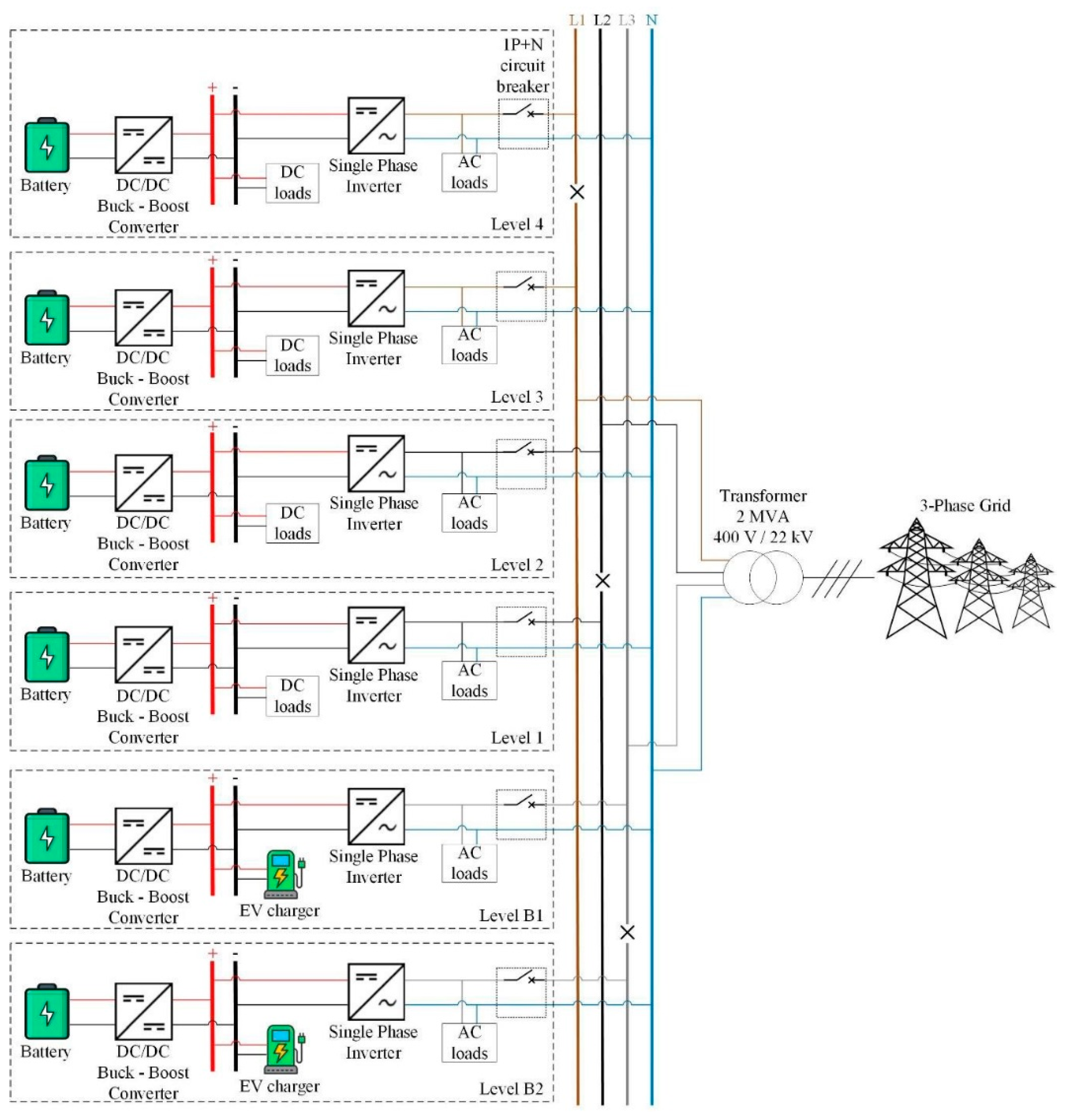
Figure 2.
SS530 lighting power density guideline.
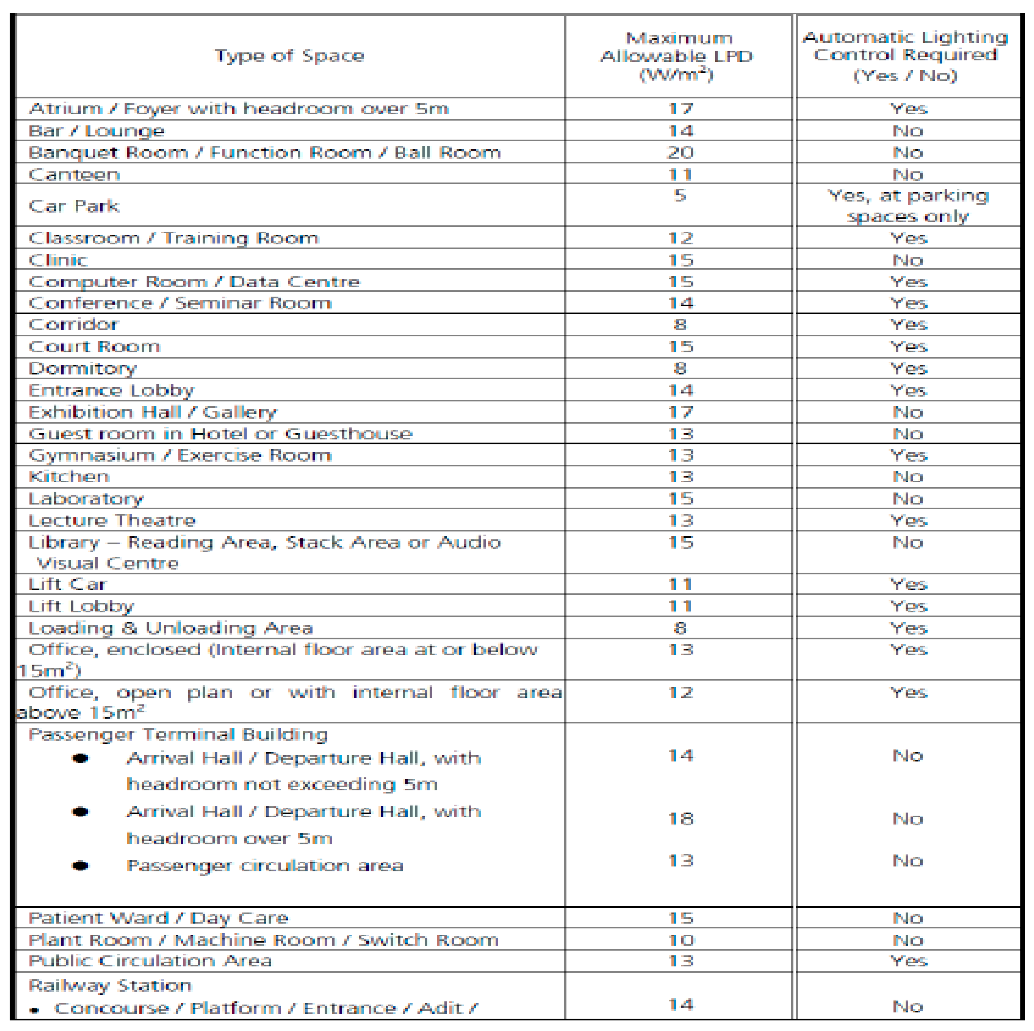
Figure 3.
Proposed topology used in BESS.
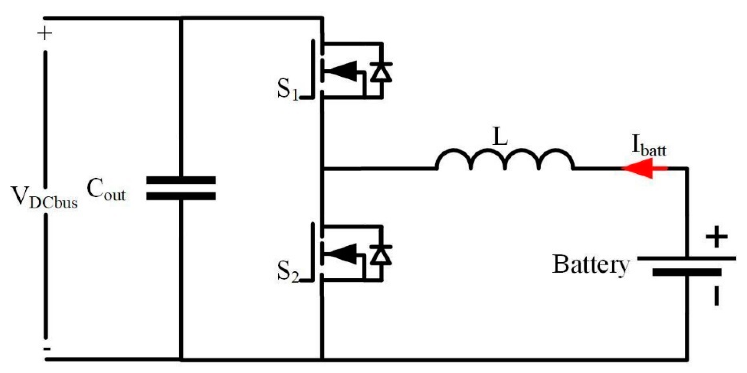
Figure 4.
Proposed control algorithm used to control BESS.
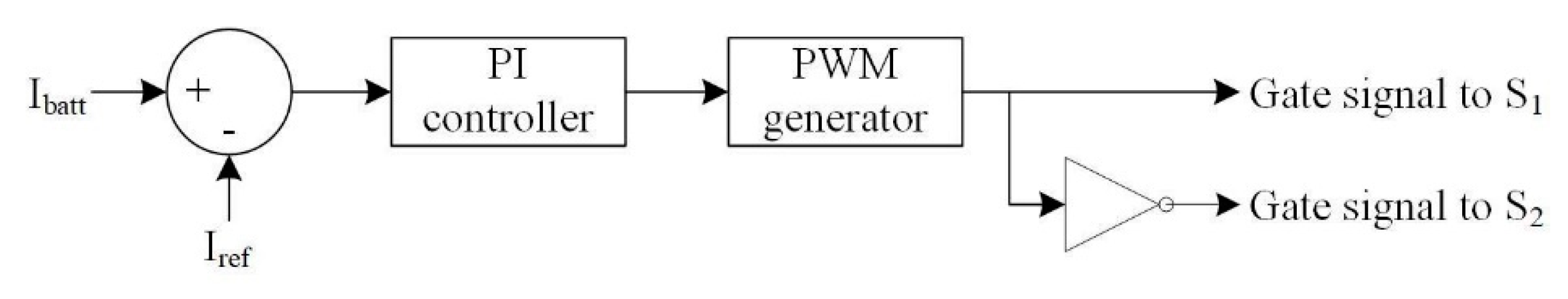
Figure 5.
Proposed topology used in single-phase inverter.
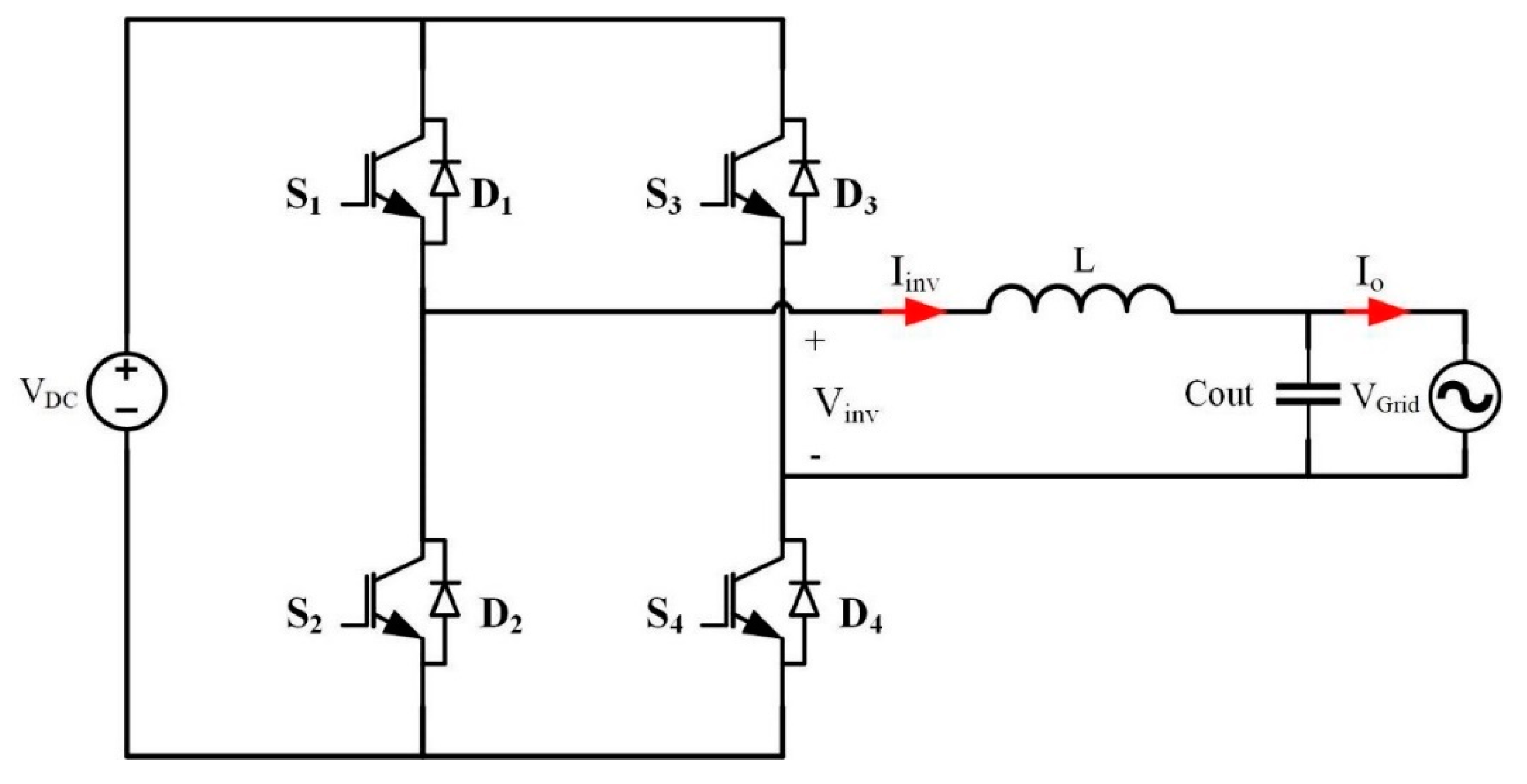
Figure 6.
Proposed topology used in single-phase inverter.
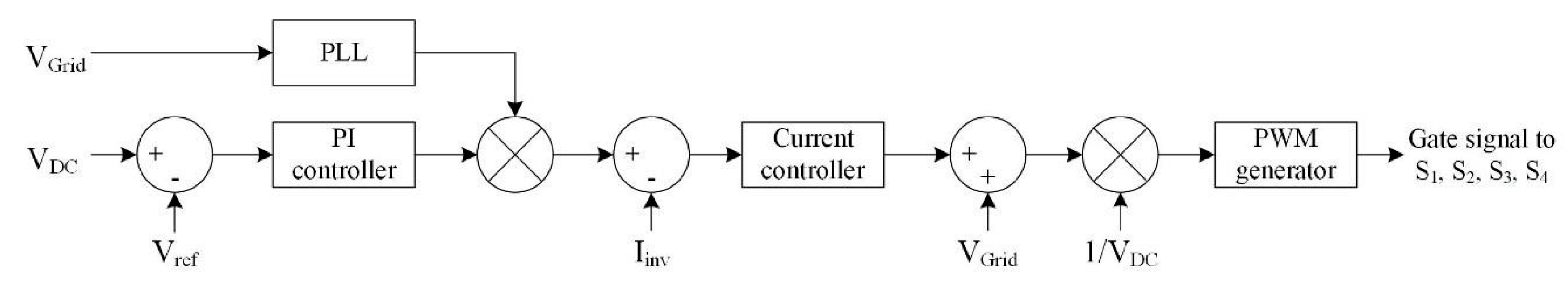
Figure 7.
Overview of nano-grid system a building at SIT Punggol campus.
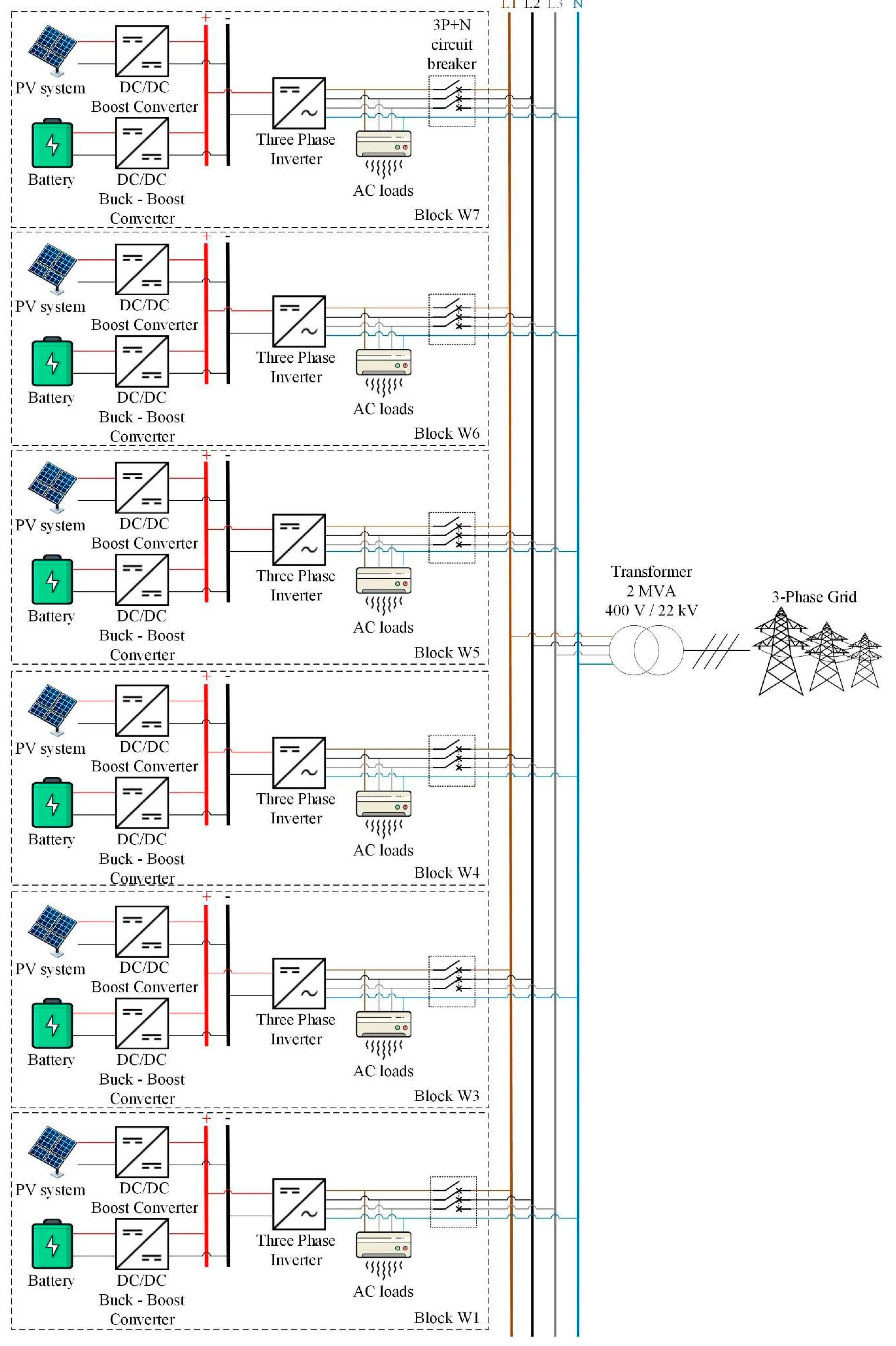
Figure 8.
Proposed topology used in solar PV boost converter.
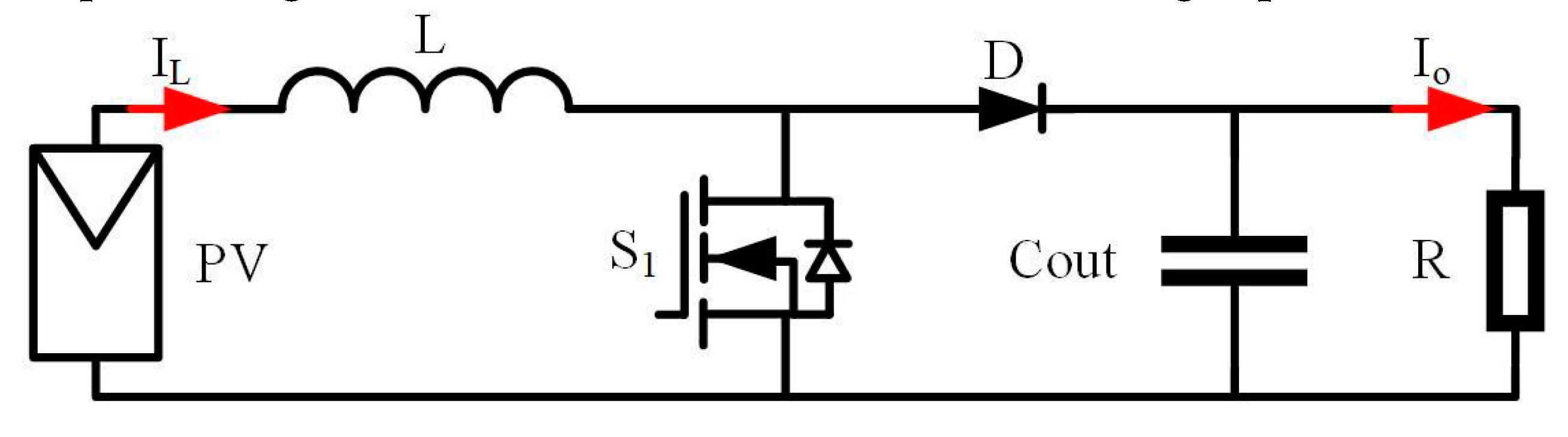
Figure 9.
Proposed control algorithm used to control boost converter.
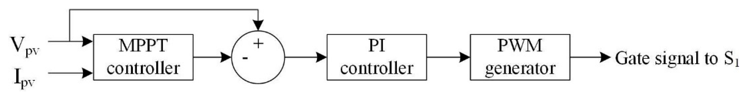
Figure 10.
Proposed P&O algorithm for MPPT operation.
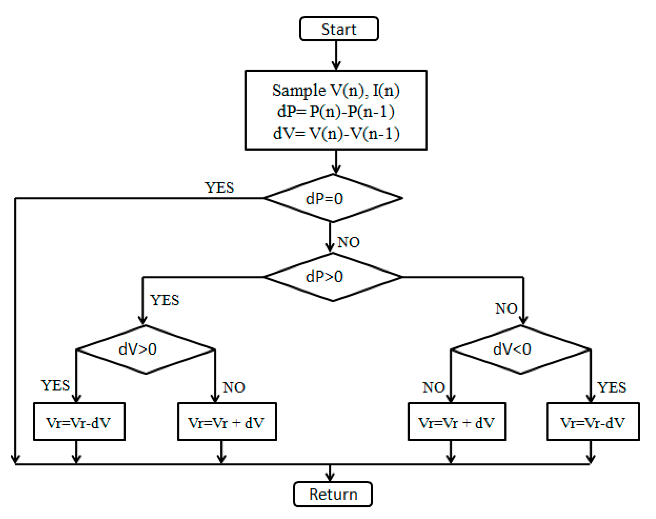
Figure 11.
Proposed topology used in three-phase inverter.
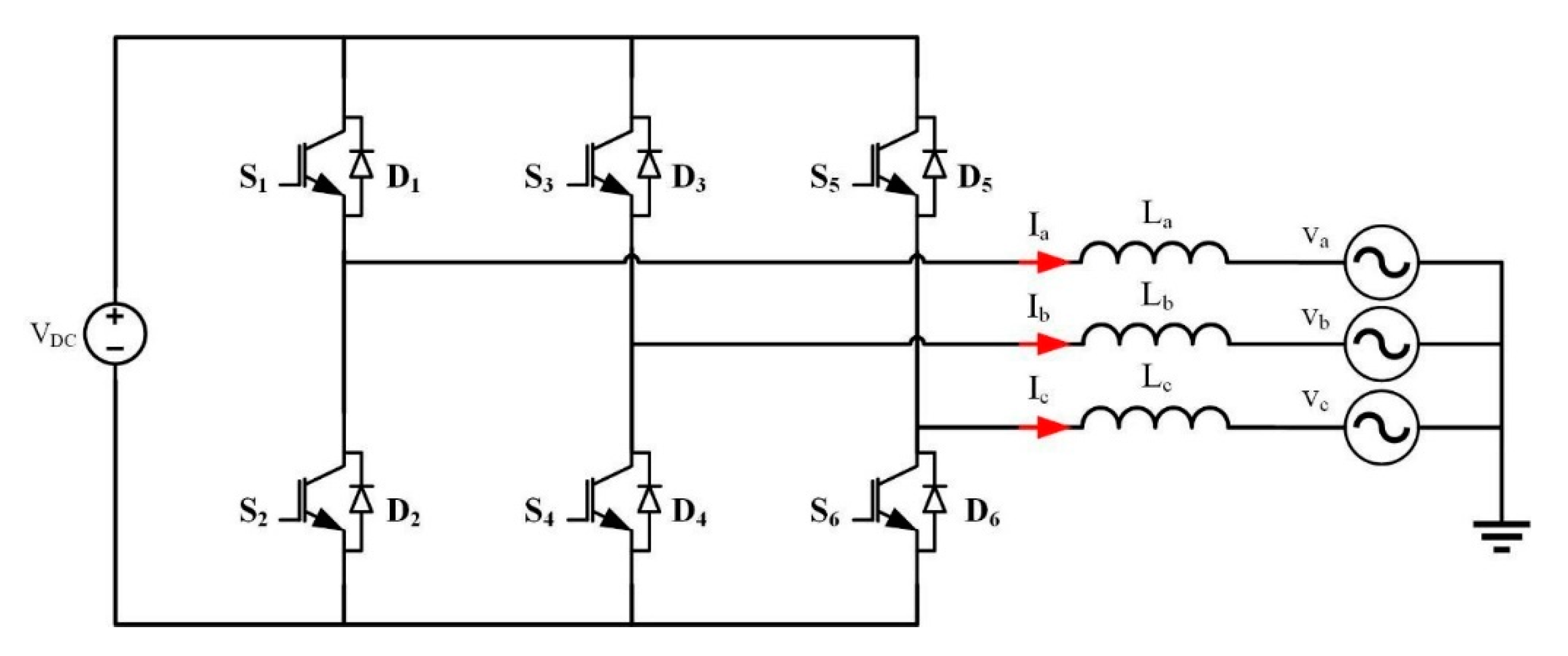
Figure 12.
Proposed control algorithm used to control three-phase inverter.
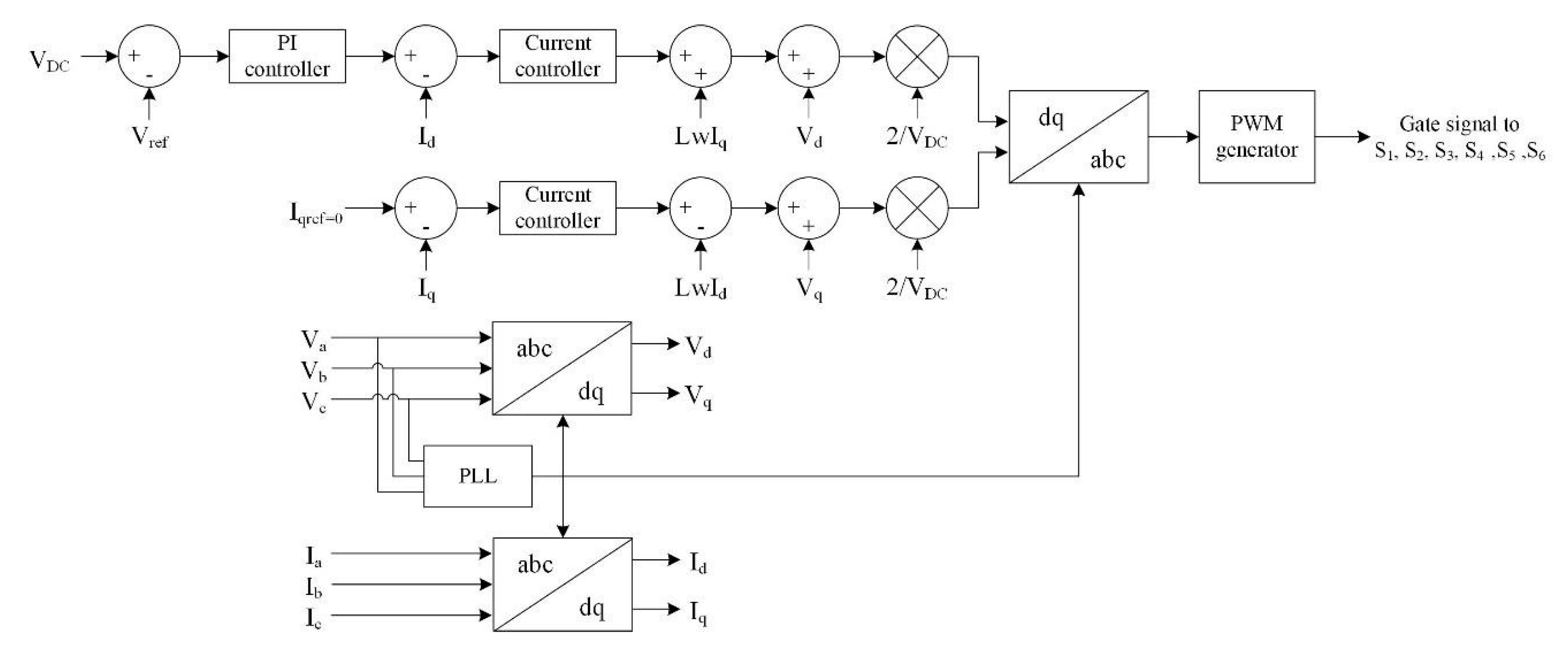
Figure 13.
Simulation model of BESS integration with single-phase inverter.
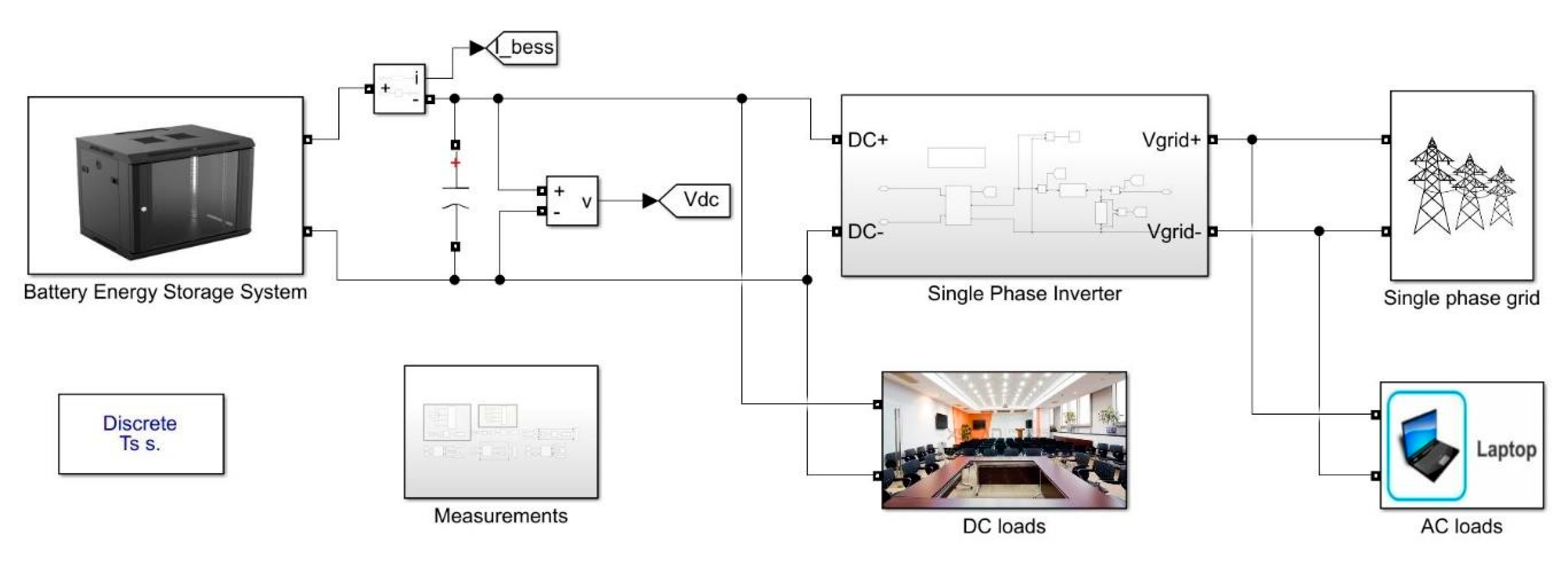
Figure 14.
Load demand estimation of DC and AC loads for pico-grid system.
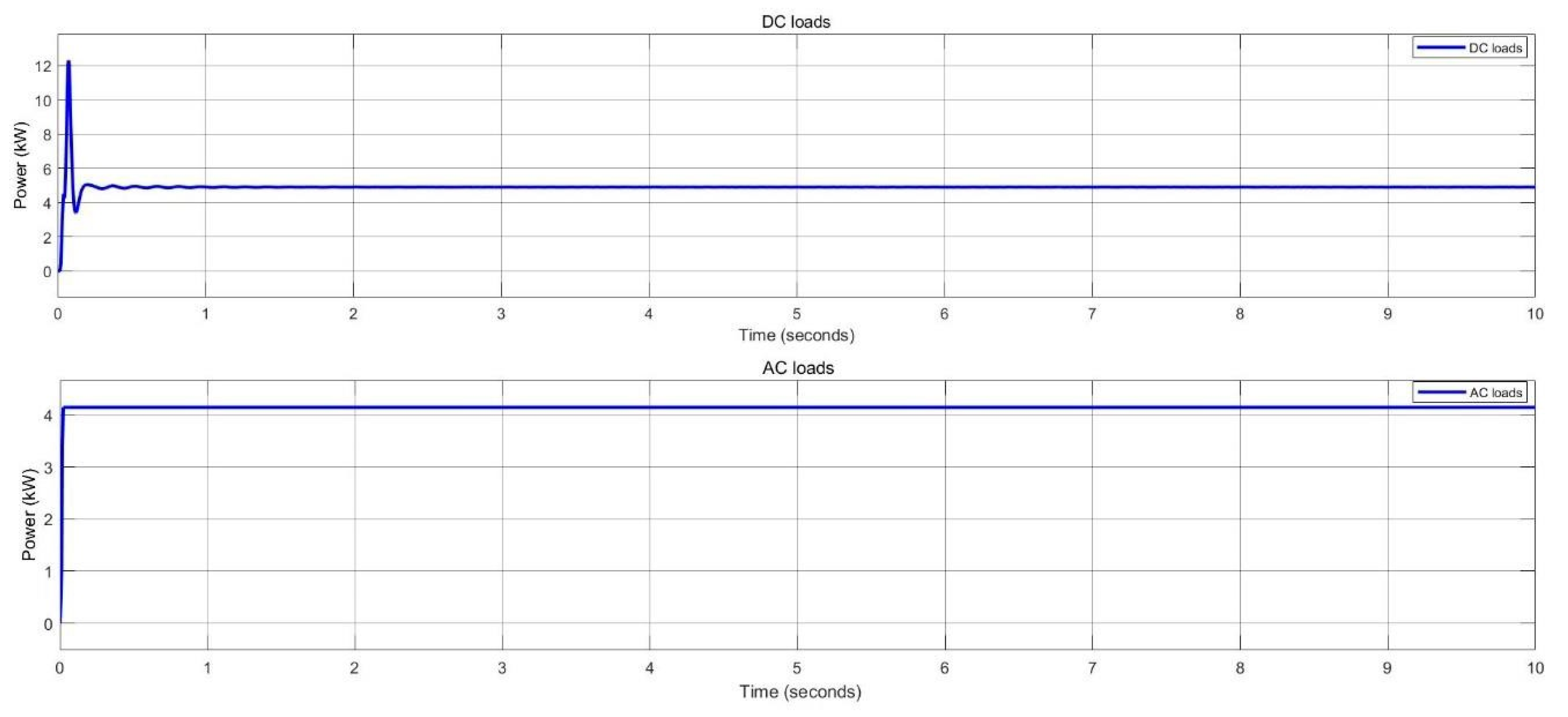
Figure 15.
The SOC level of the BESS during discharging in pico-grid system.
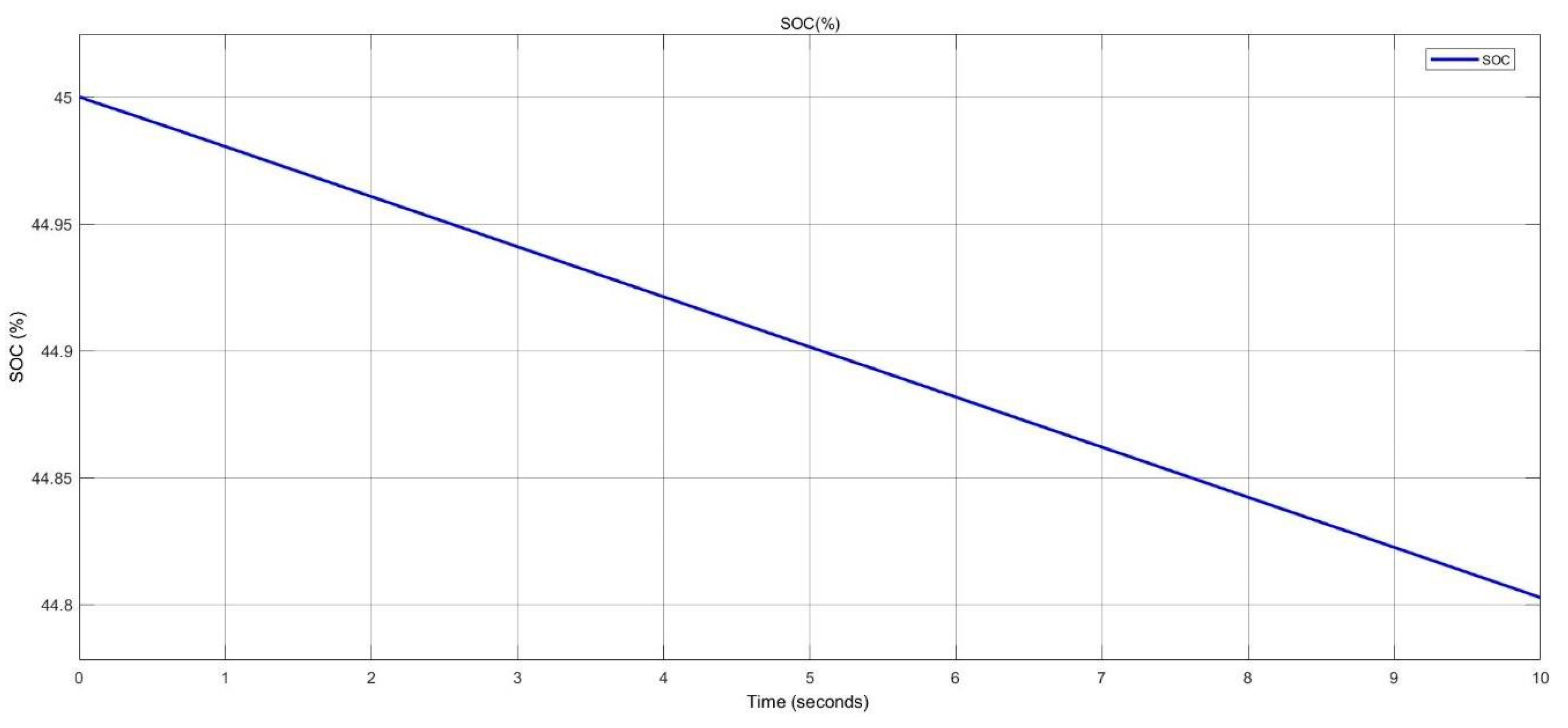
Figure 16.
The battery voltage of the BESS during discharging in pico-grid system.
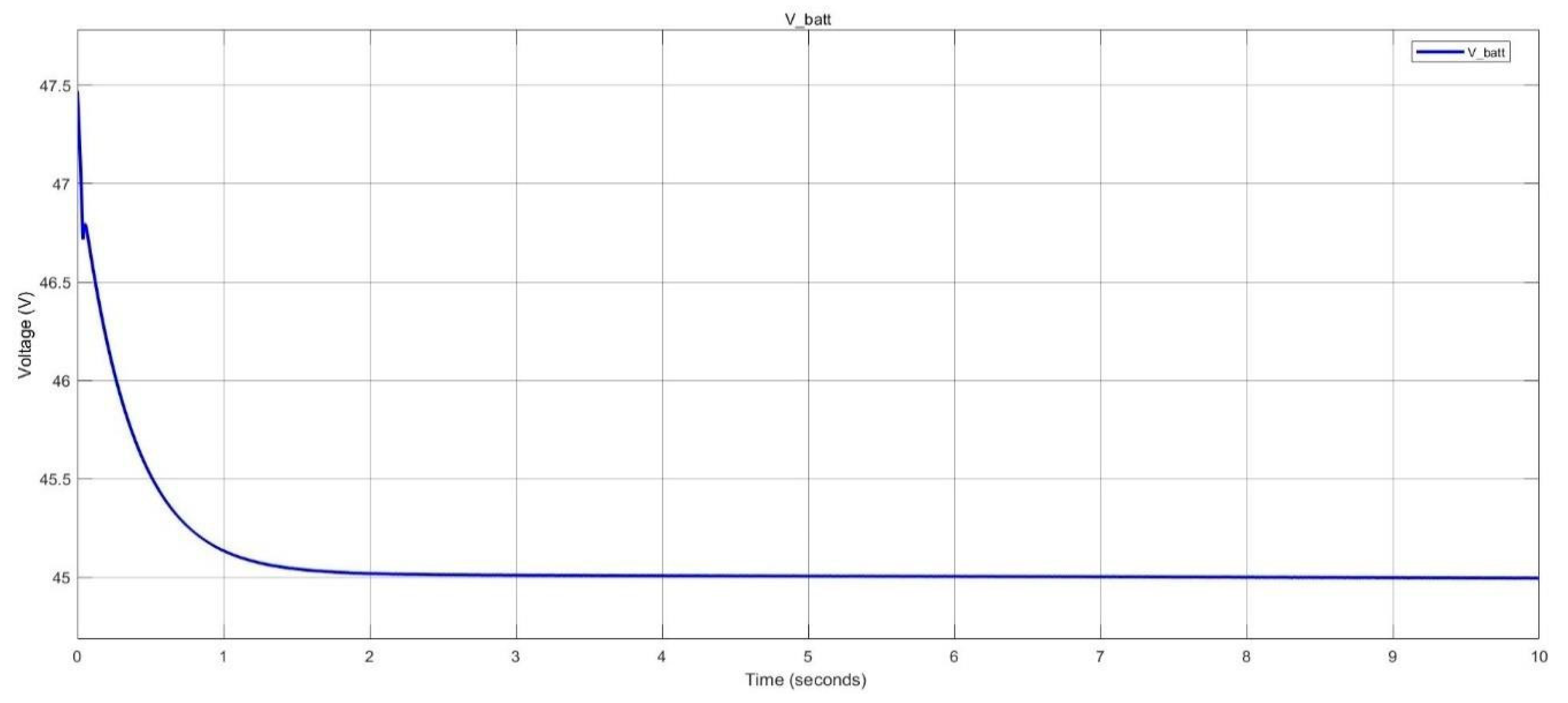
Figure 17.
Battery current of BESS during discharging in pico-grid system.
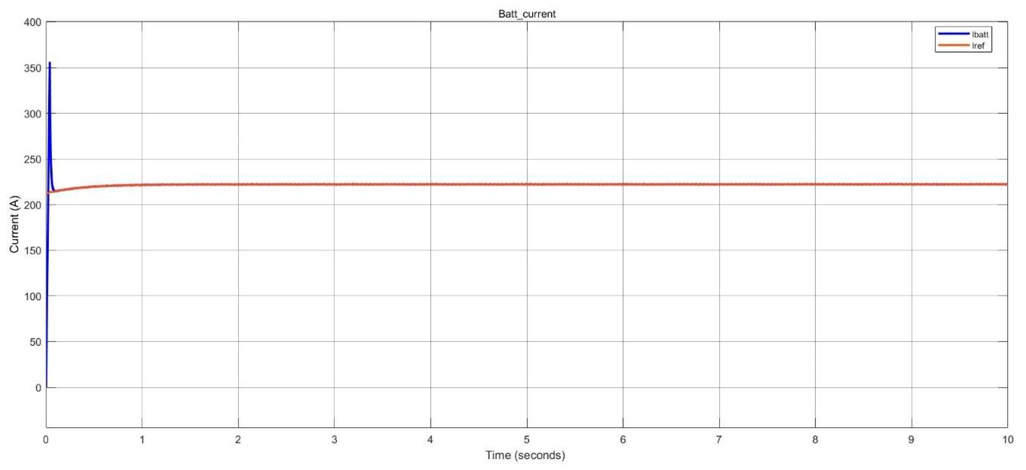
Figure 18.
Battery capacity of BESS during discharging in pico-grid system.
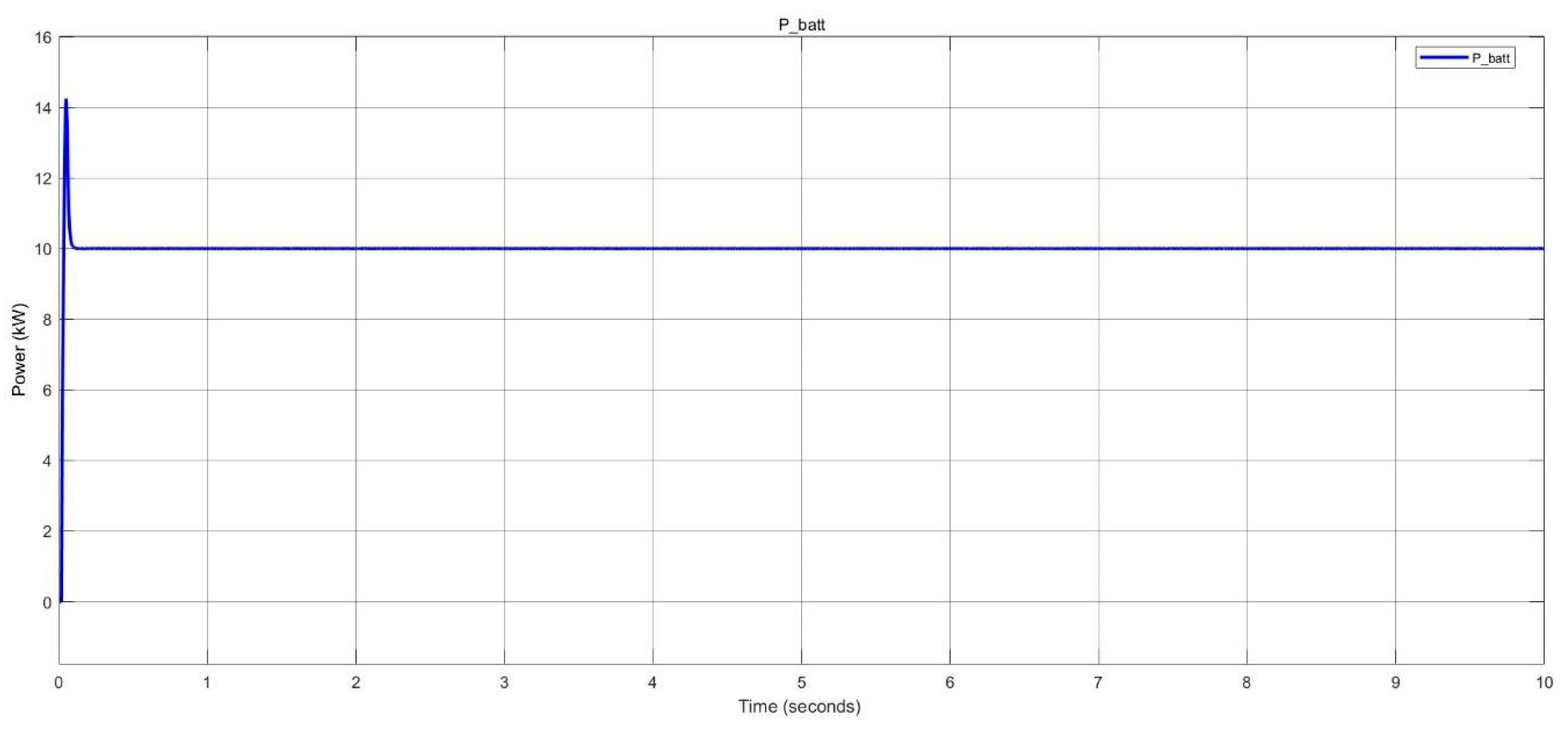
Figure 19.
Voltage level at DC busbar in pico-grid system.
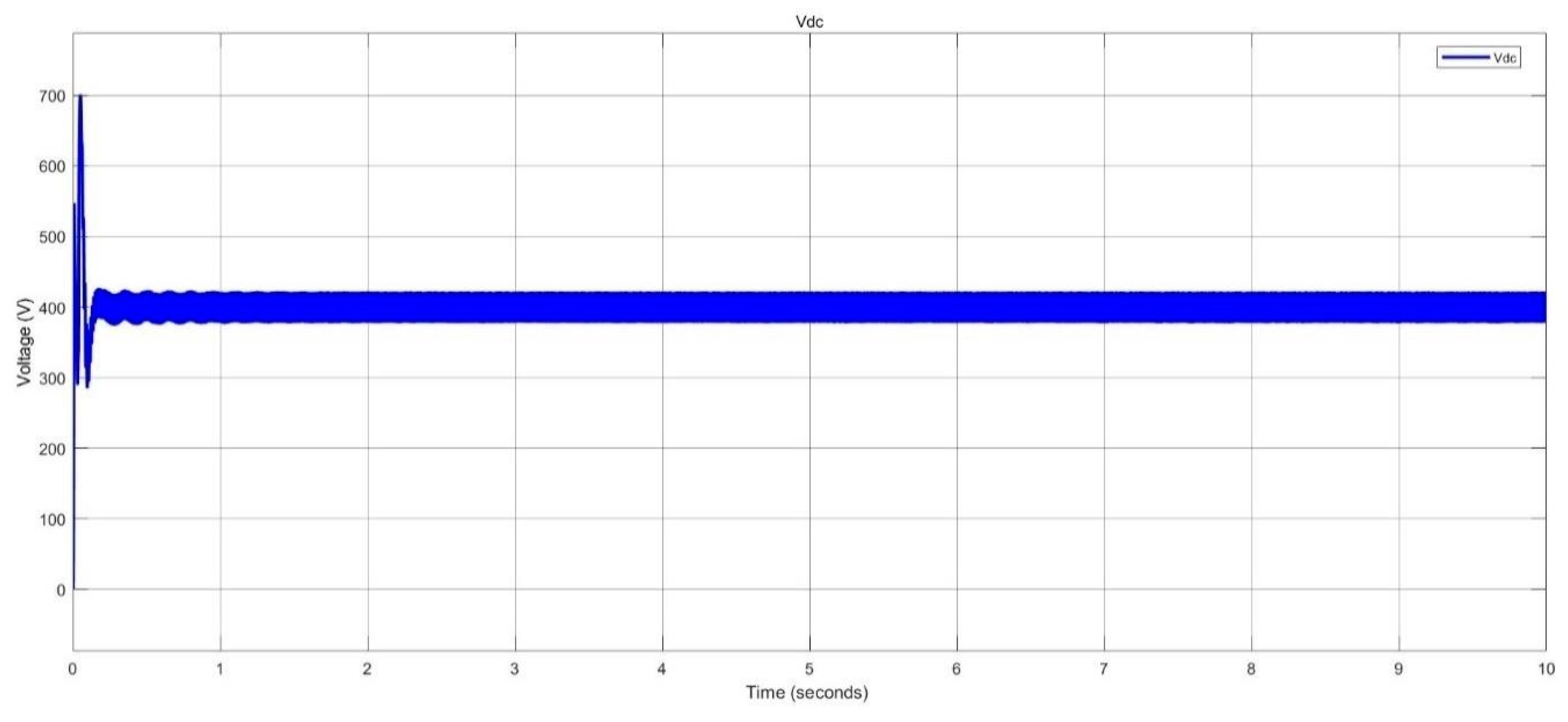
Figure 20.
Surplus power delivered to the grid in pico-grid system.
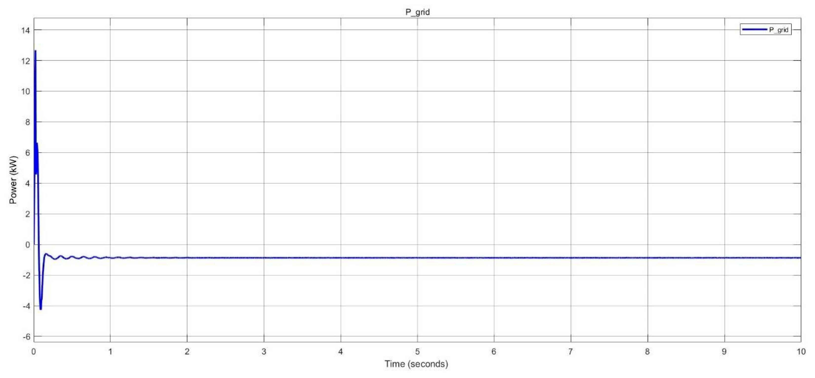
Figure 21.
SOC level of the BESS during charging in pico-grid system.
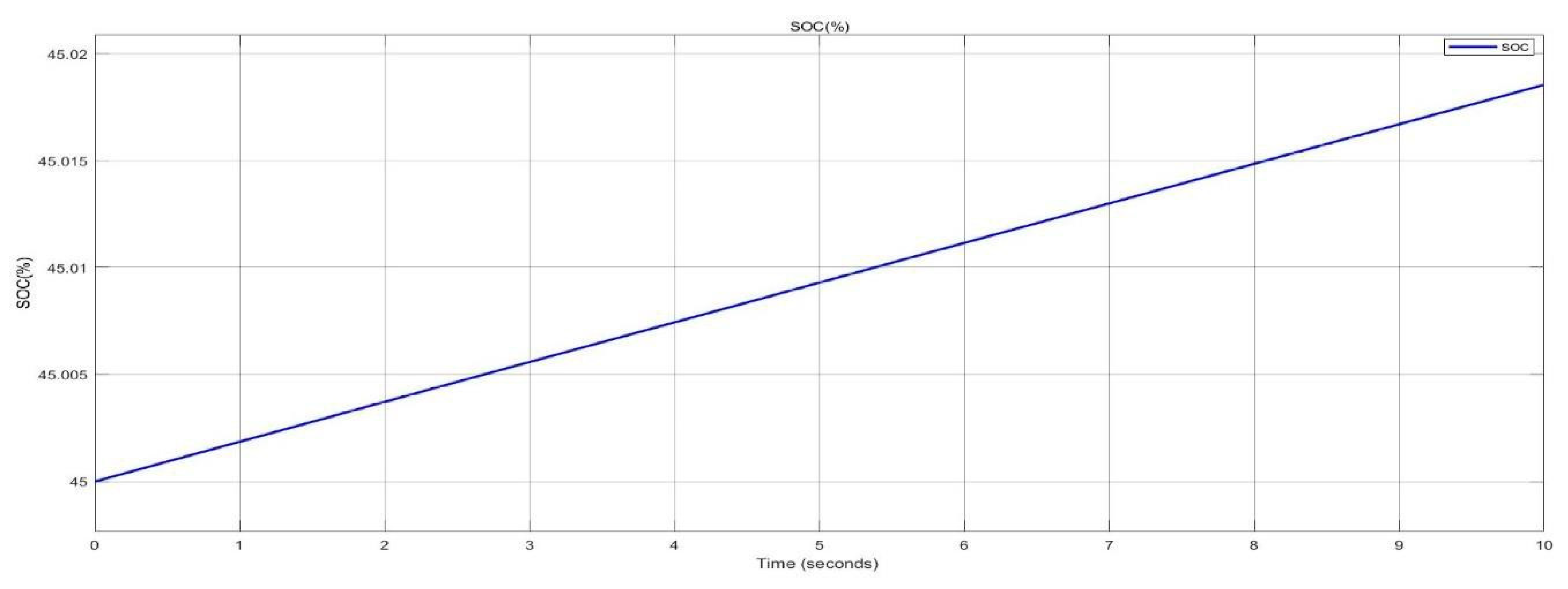
Figure 22.
Battery voltage of the BESS during charging in pico-grid system.
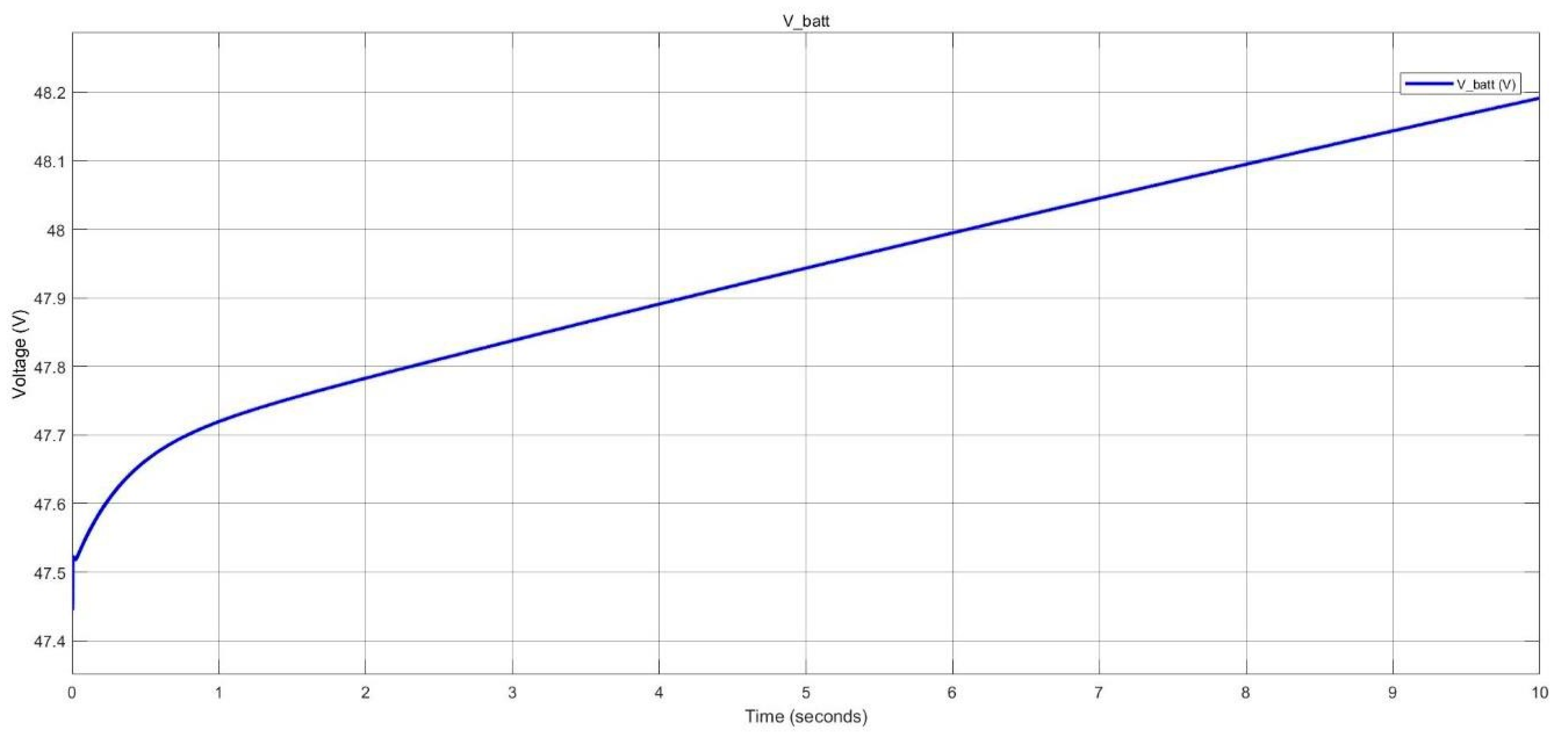
Figure 23.
Battery voltage of the BESS during charging in pico-grid system.
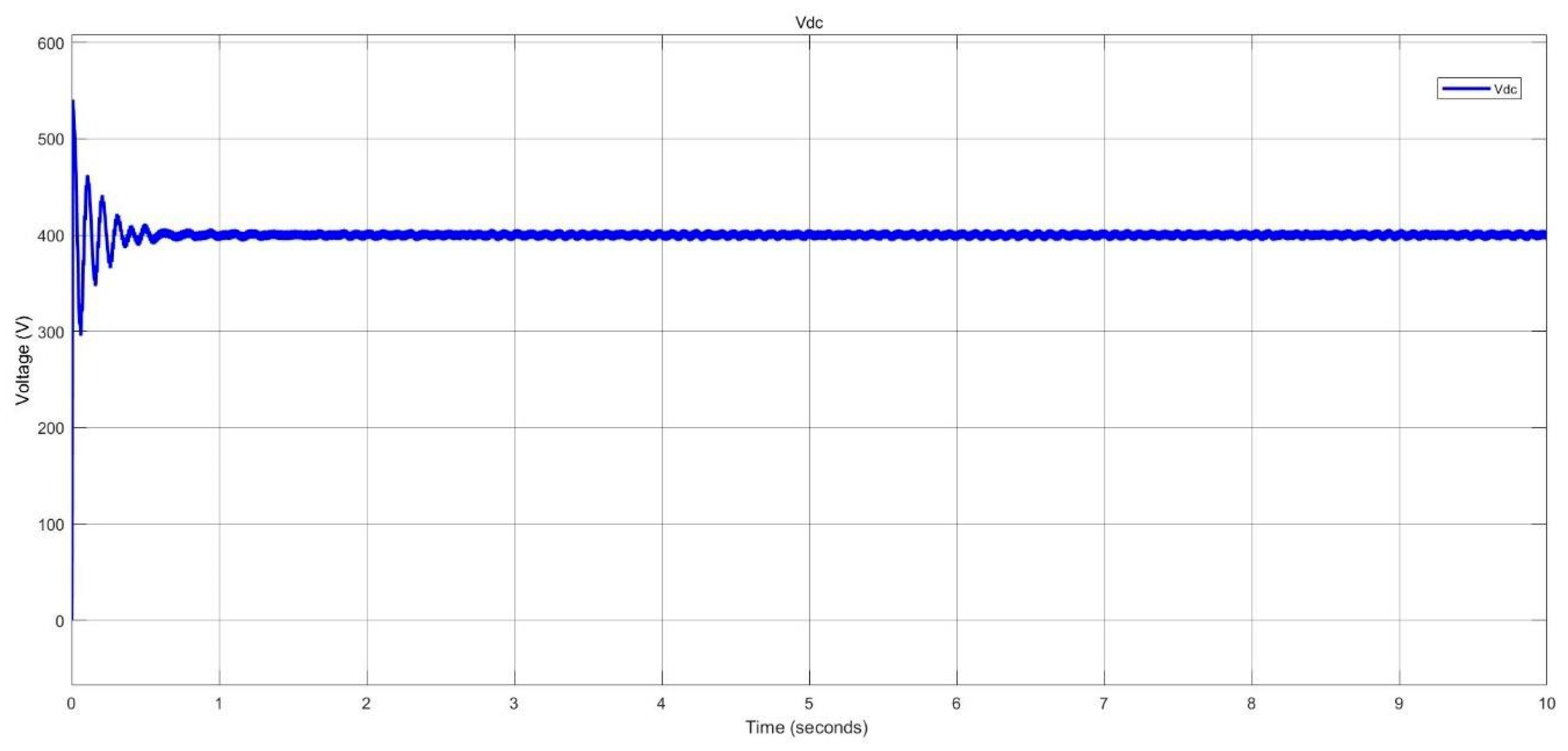
Figure 24.
Battery current of BESS during charging in pico-grid system.
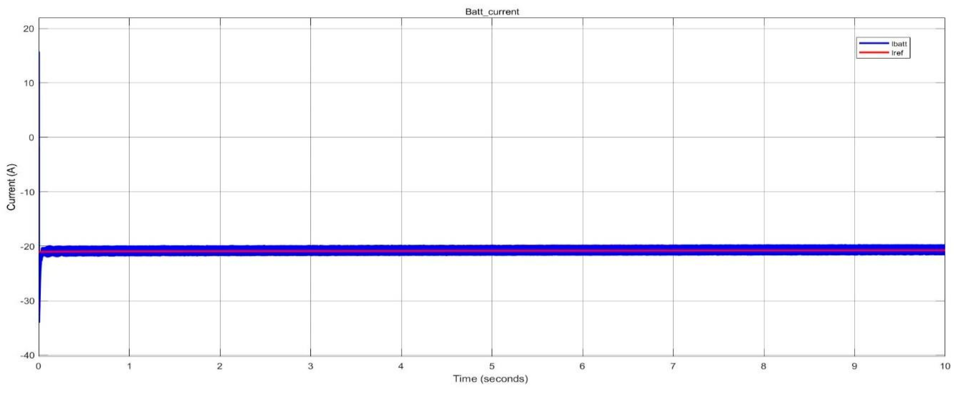
Figure 25.
Battery capacity of BESS during charging in pico-grid system.
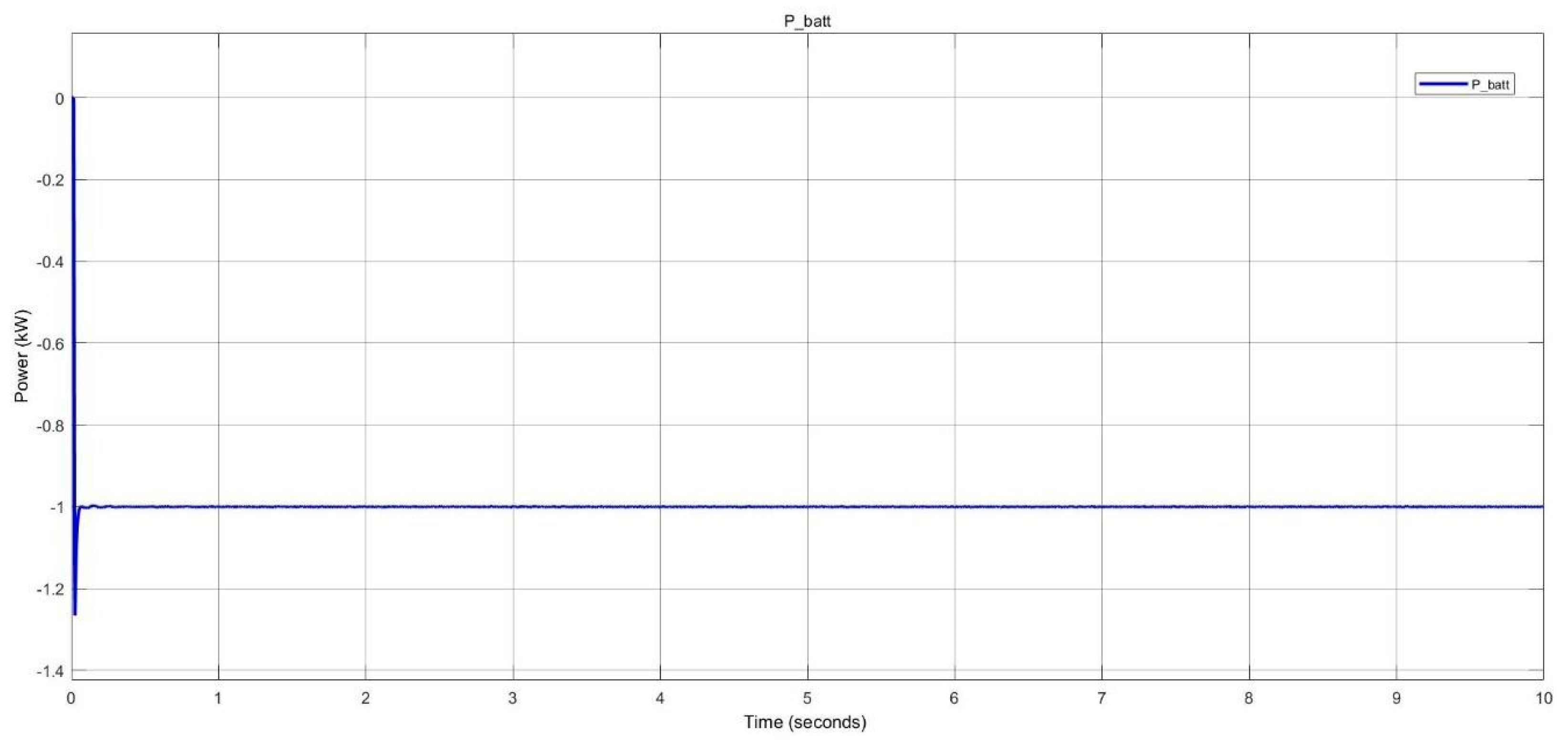
Figure 26.
Drawing power from the grid to charge the battery in pico-grid system.
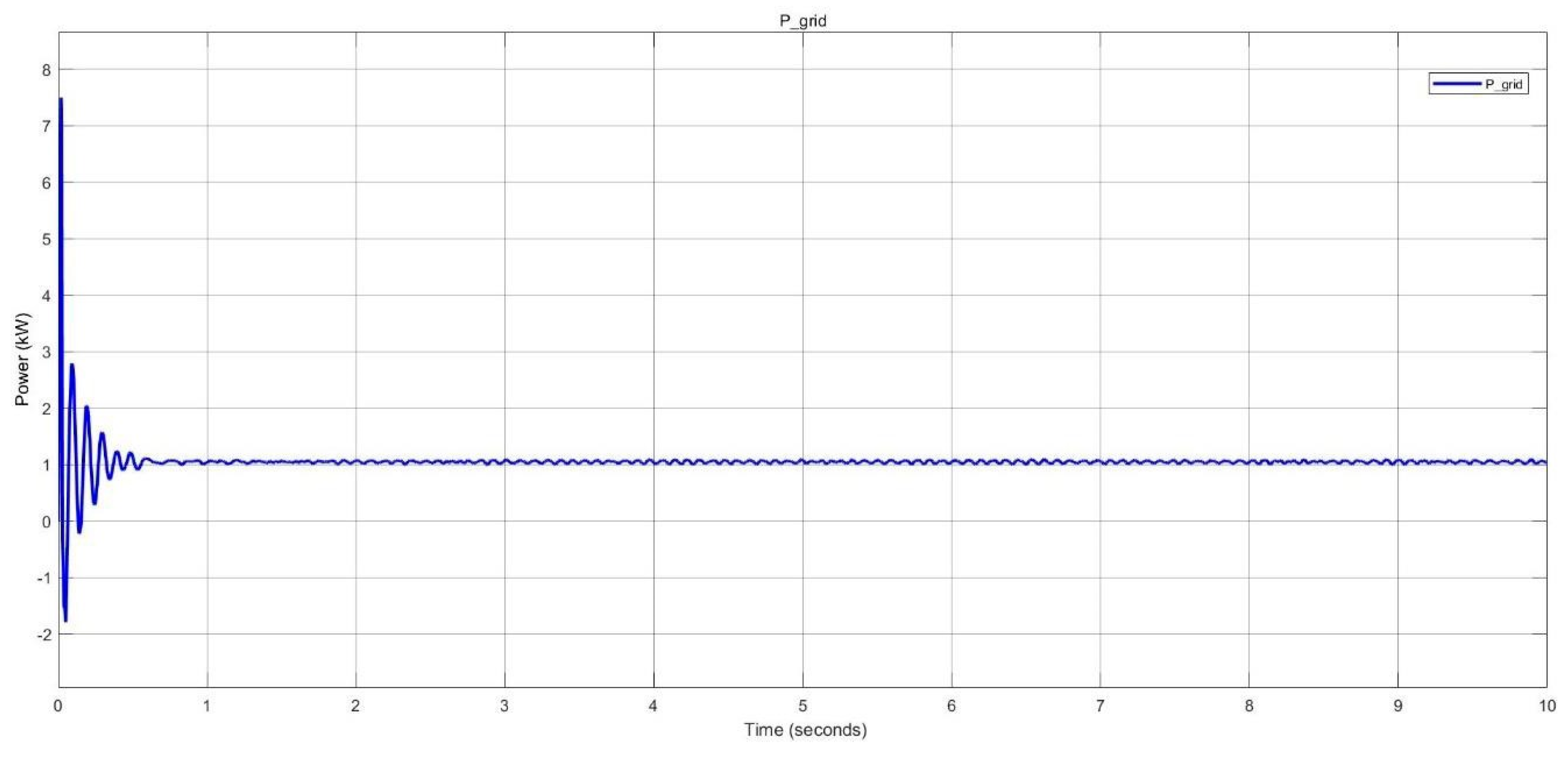
Figure 27.
Two parallel pico-grids connected to the single-phase grid.
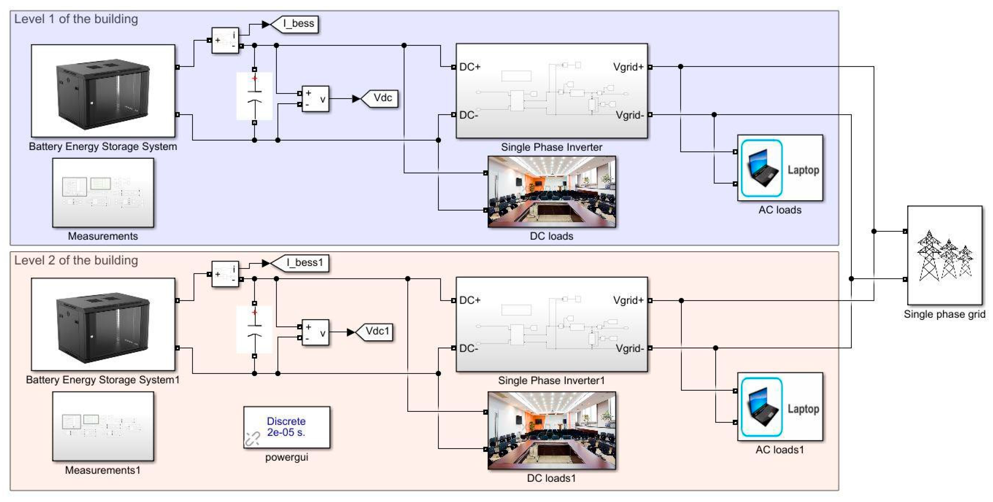
Figure 28.
DC and AC loads before increase for two pico-grids system.
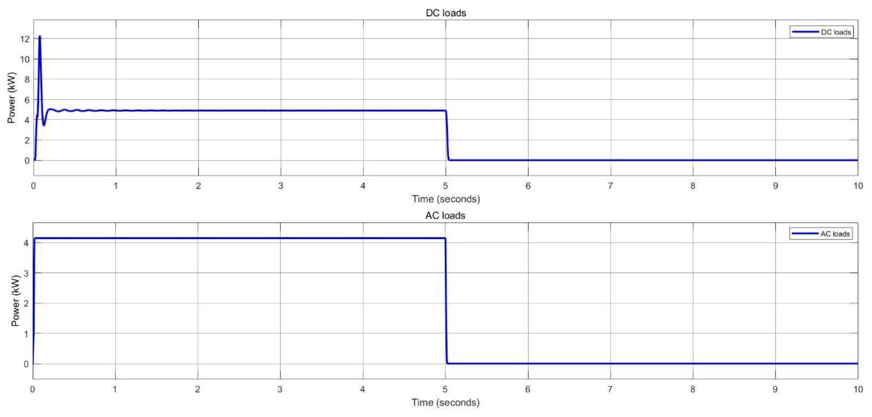
Figure 29.
DC and AC loads before increase for two pico-grids system.
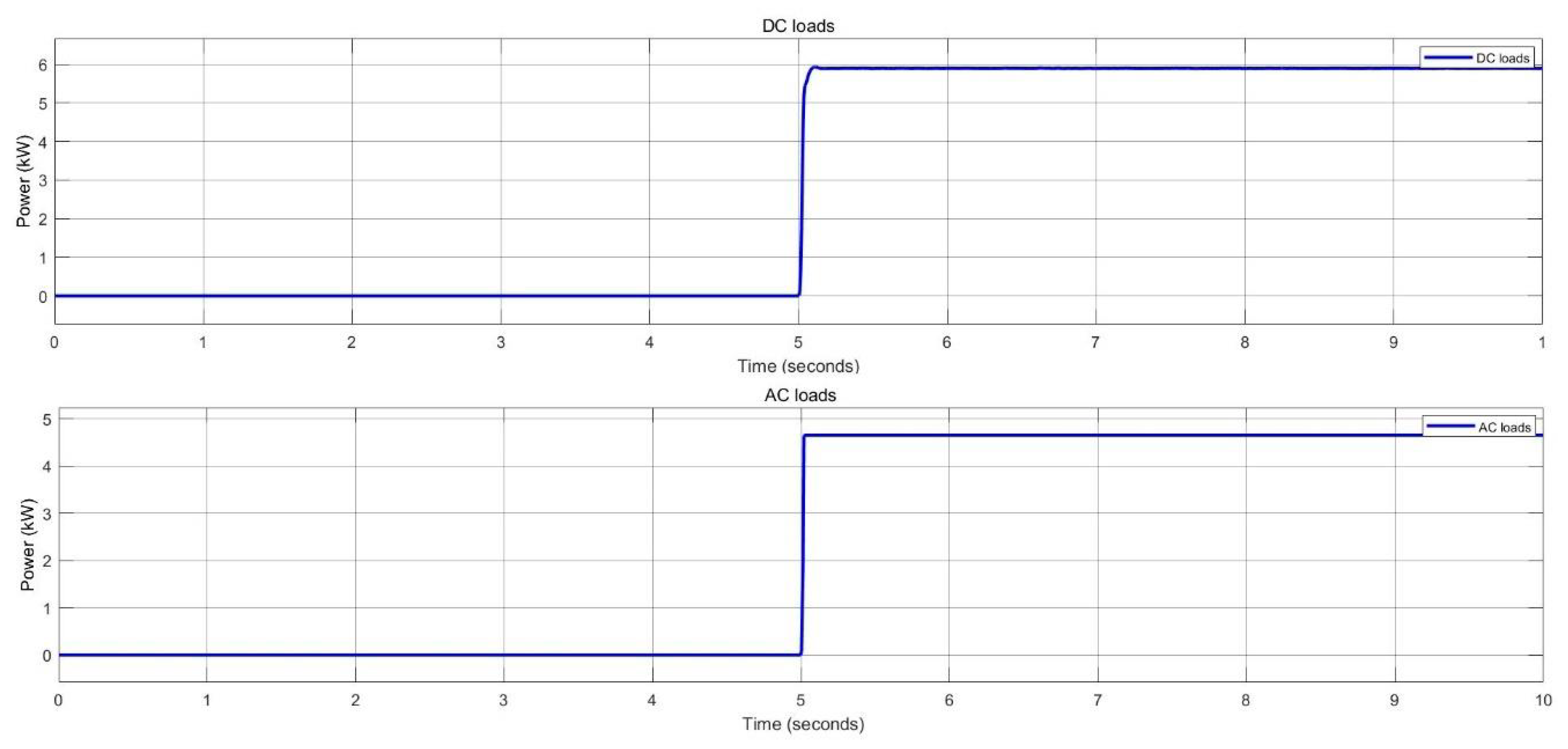
Figure 30.
Surplus power from the system sent to the grid for two pico-grids system.
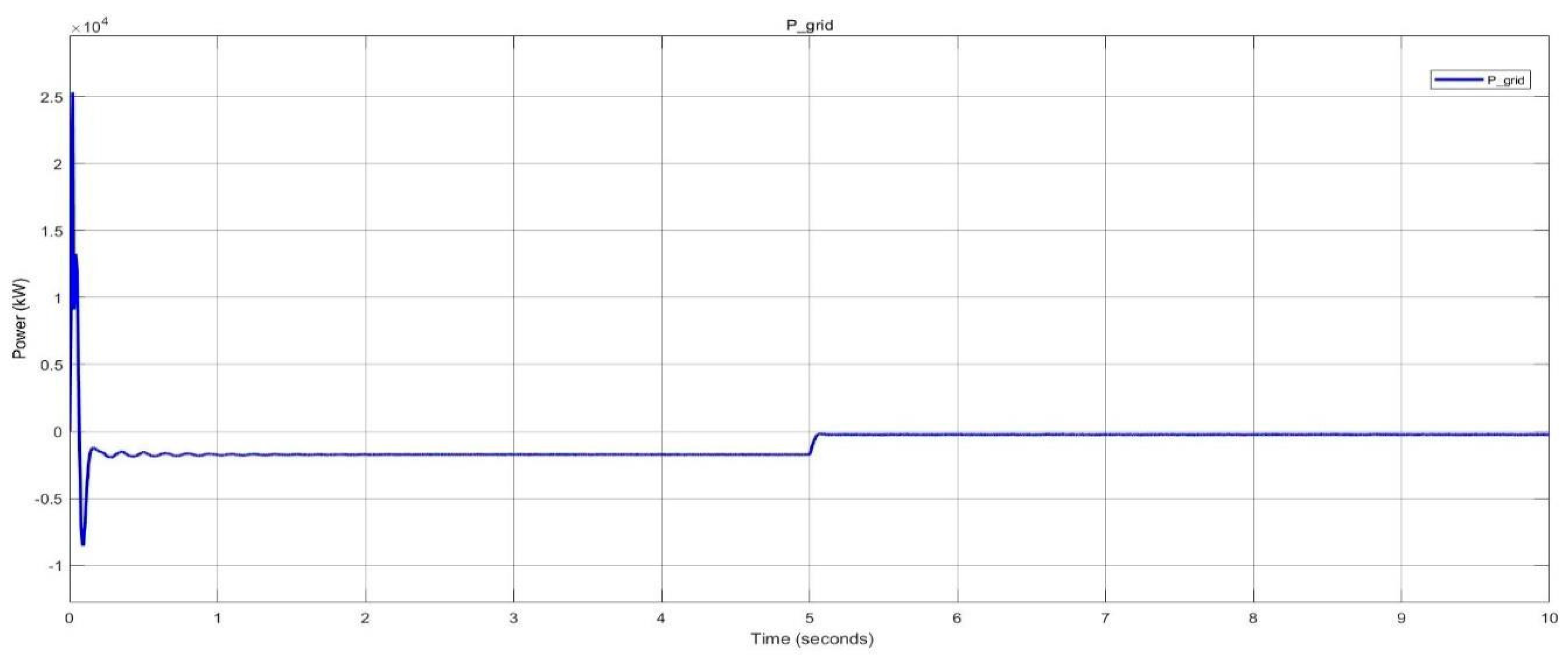
Figure 31.
Simulation model of integration of solar PV, BESS with three-phase inverter.
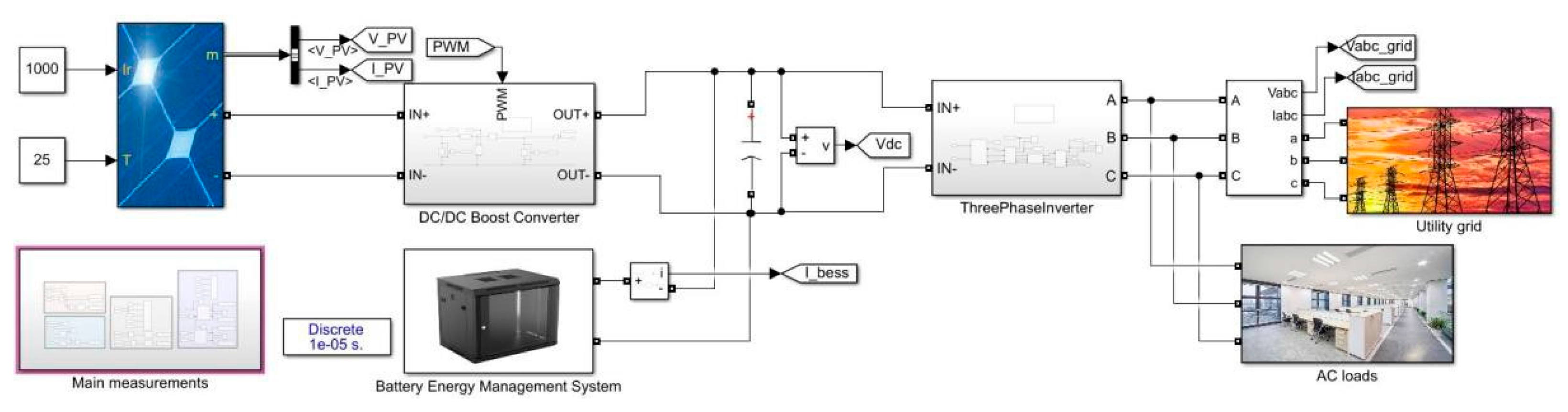
Figure 32.
Solar PV array waveform.
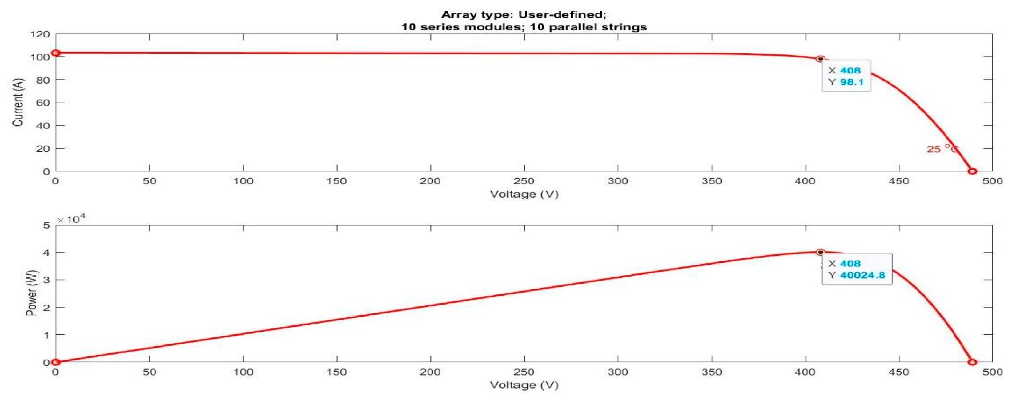
Figure 33.
Load demand estimation of AC loads in nano-grid system.
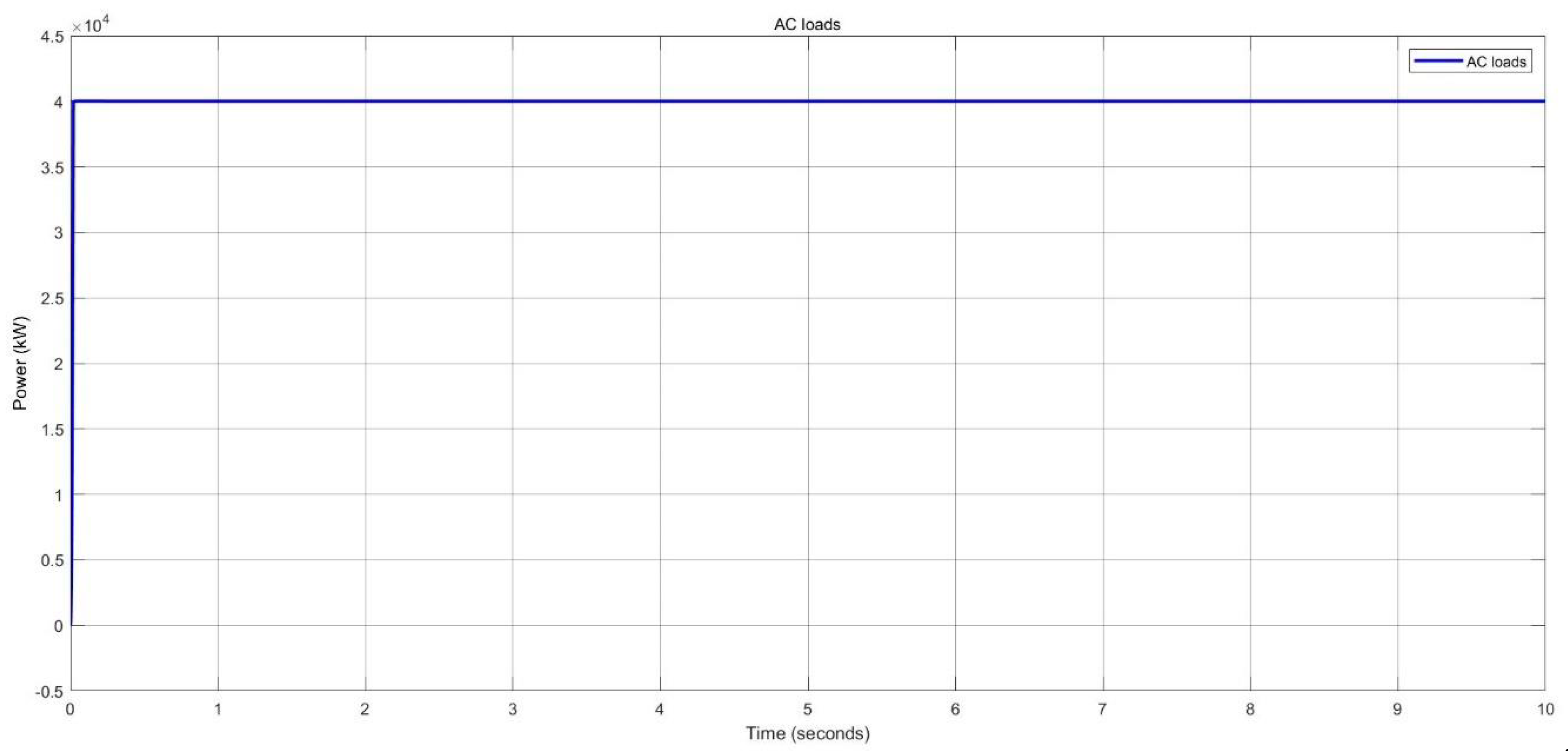
Figure 34.
SOC of battery during discharging in nano-grid system.
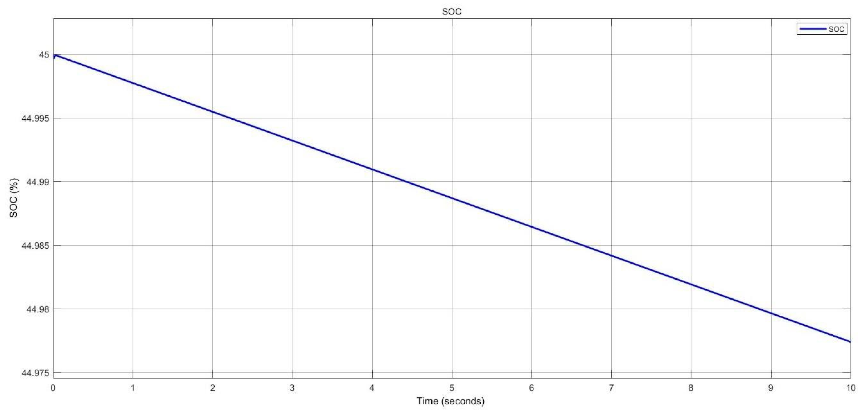
Figure 35.
Battery voltage of the BESS during discharging in nano-grid system.
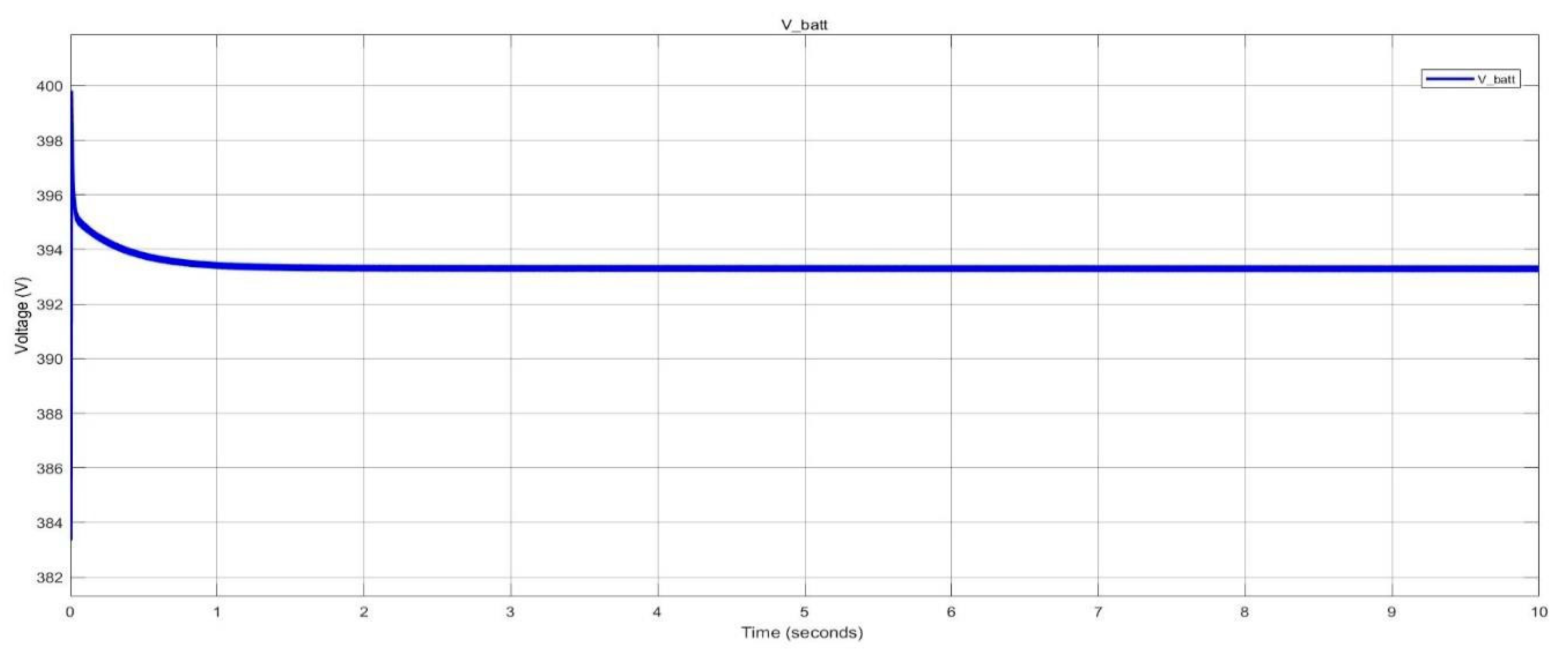
Figure 36.
Battery current of BESS during discharging in nano-grid system.
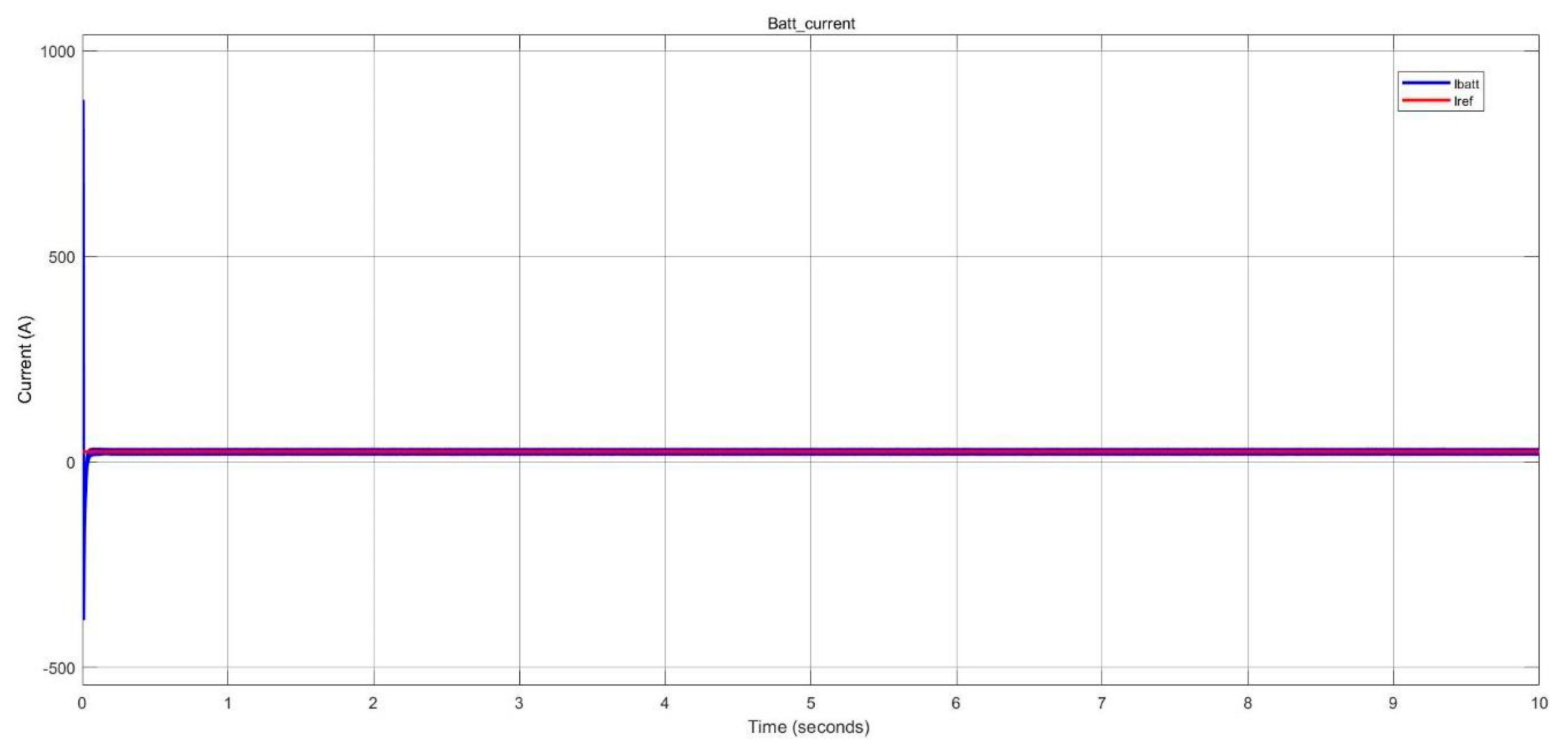
Figure 37.
Battery capacity of BESS during discharging in nano-grid system.
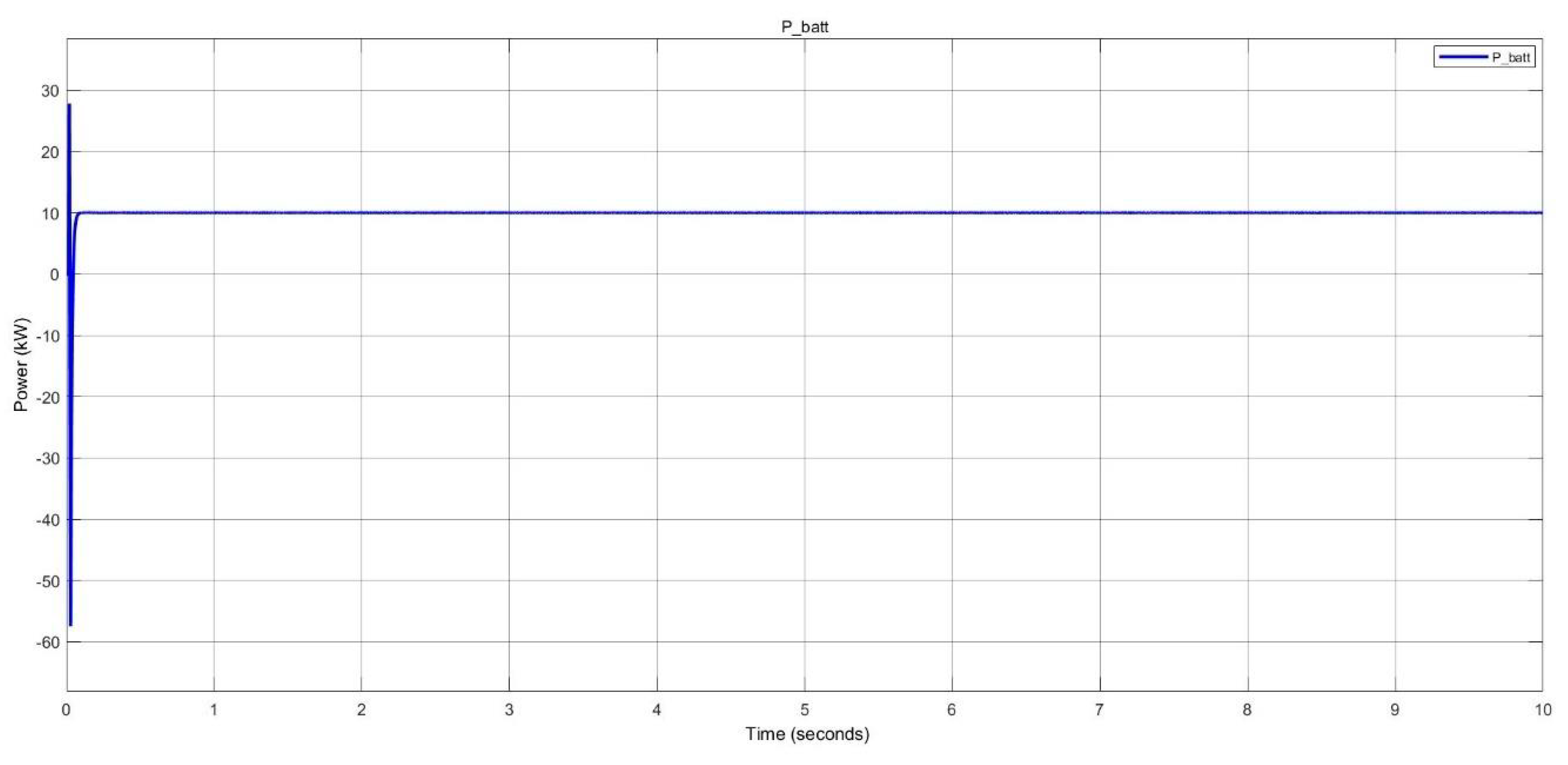
Figure 38.
Voltage level at DC busbar in nano-grid system.
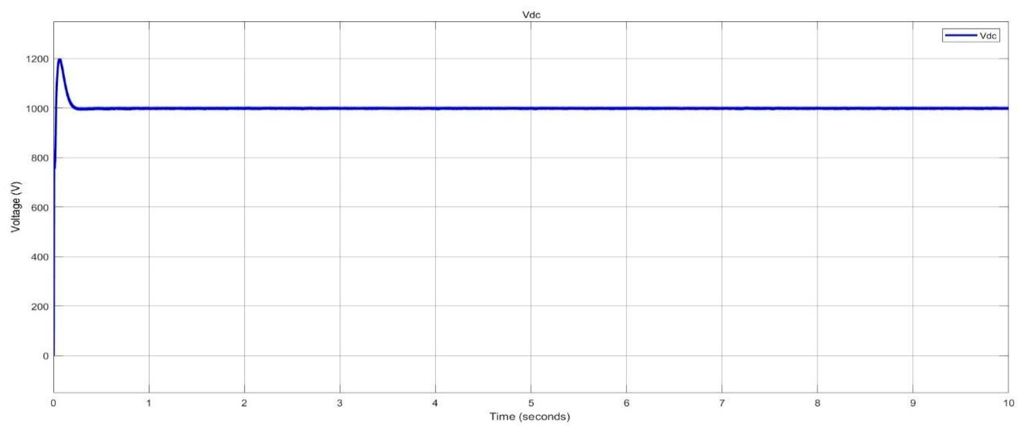
Figure 39.
Surplus power delivered to the grid in nano-grid system.
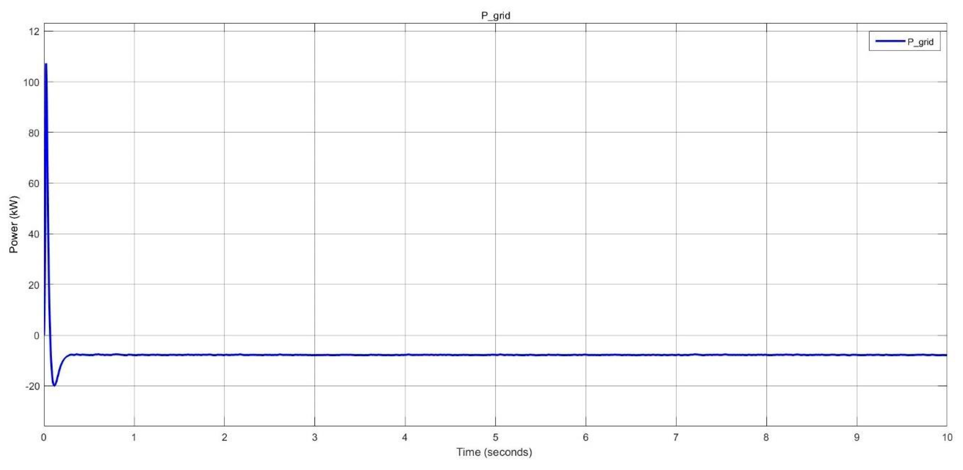
Figure 40.
Simulation model to demonstrate charging of battery.
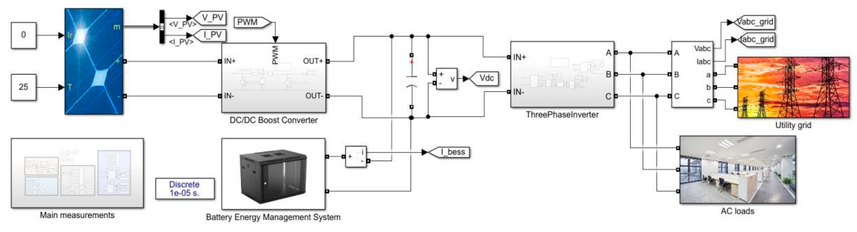
Figure 41.
SOC of battery during charging in nano-grid system.
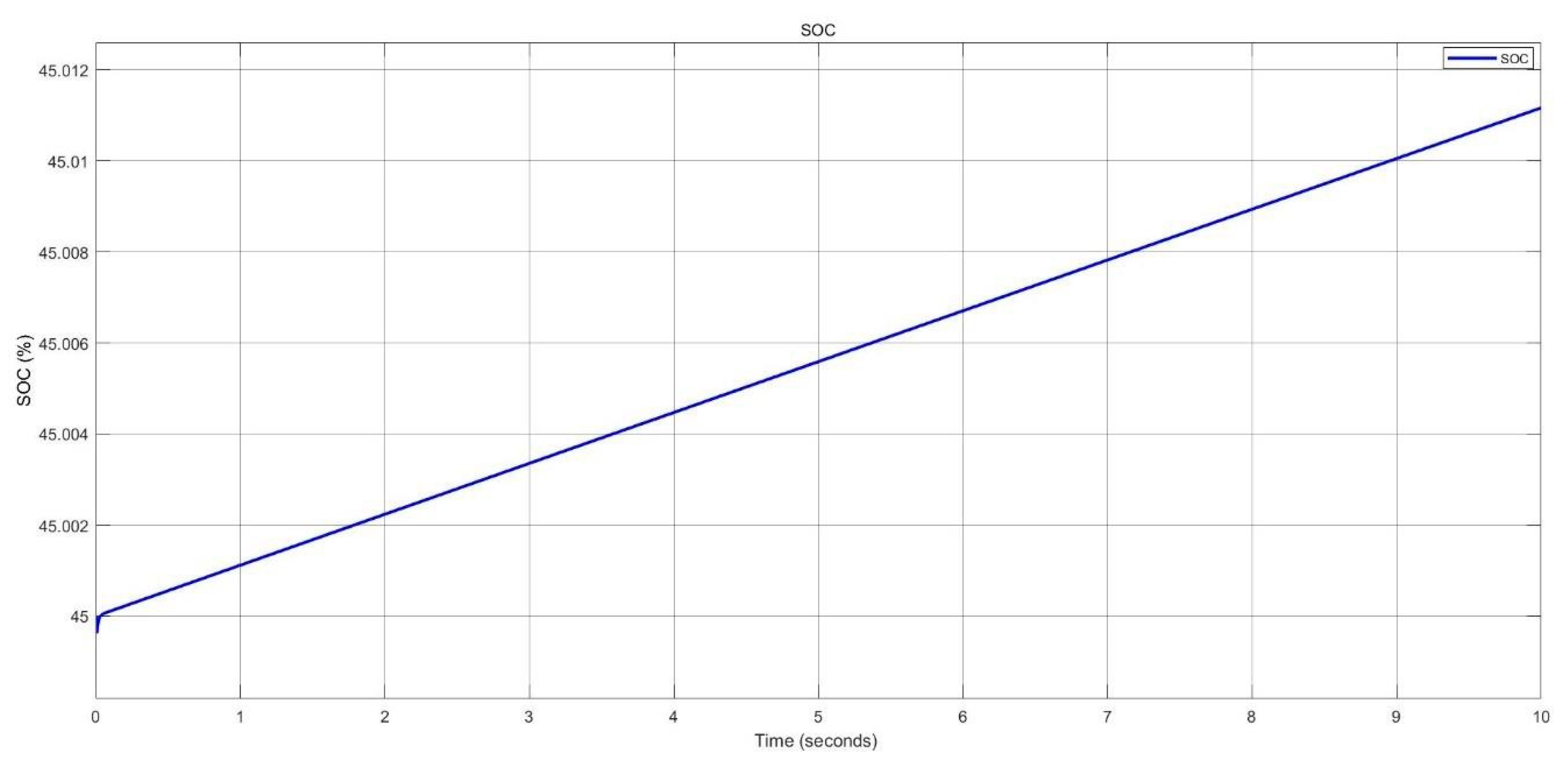
Figure 42.
Battery voltage of the BESS during charging in nano-grid system.
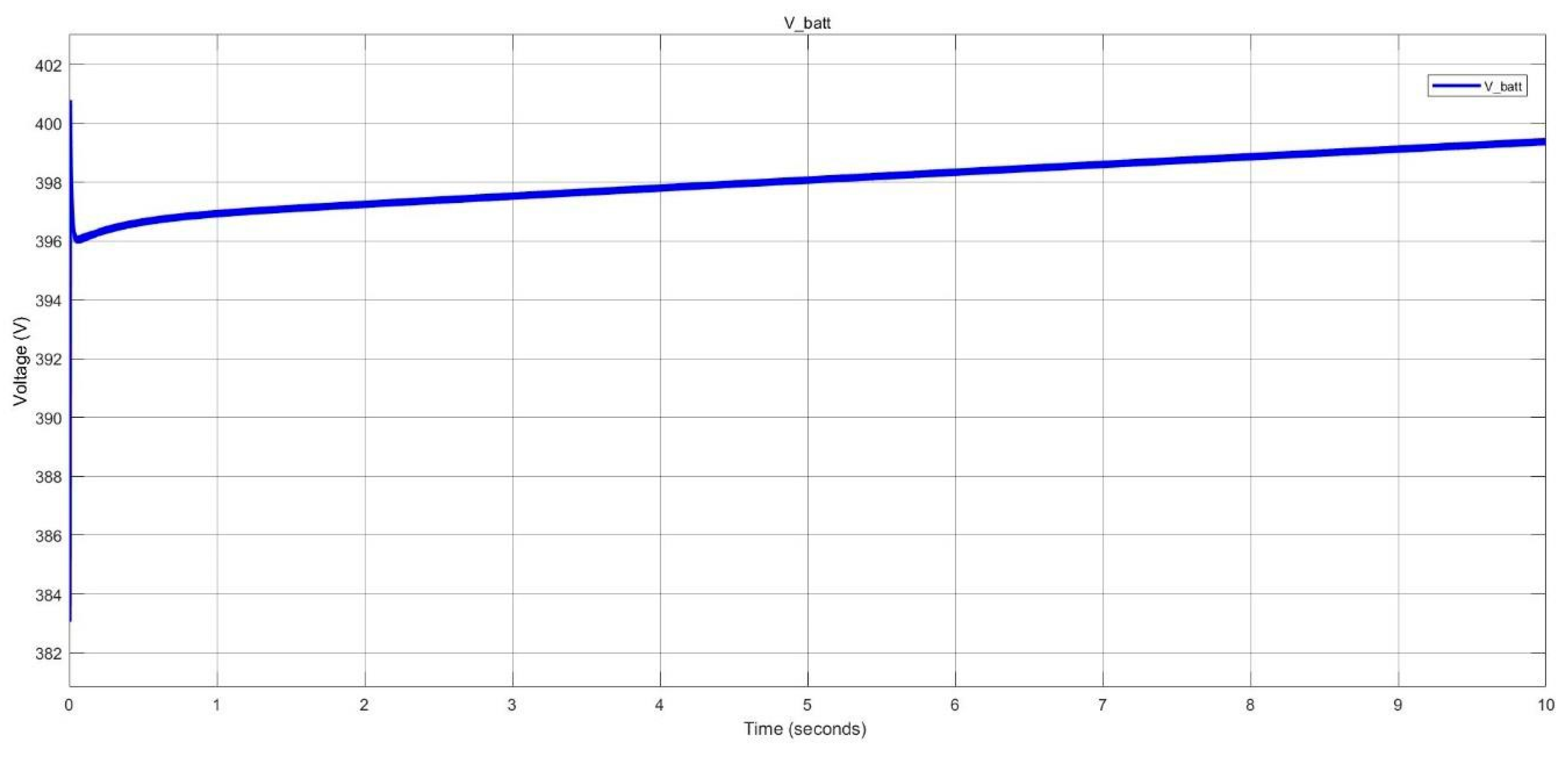
Figure 43.
Voltage level at DC busbar in nano-grid system.
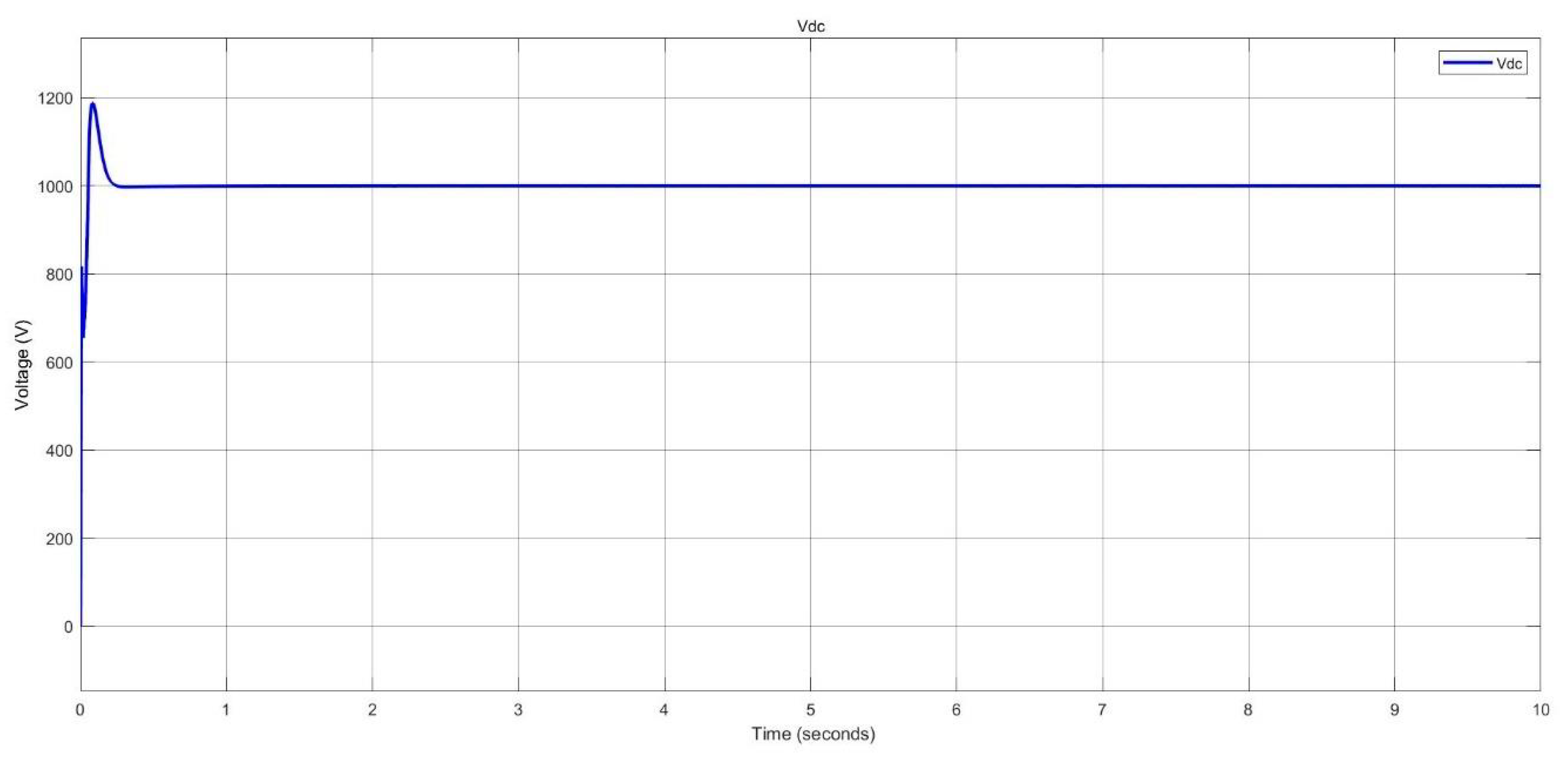
Figure 44.
Battery current of BESS during charging in nano-grid system.
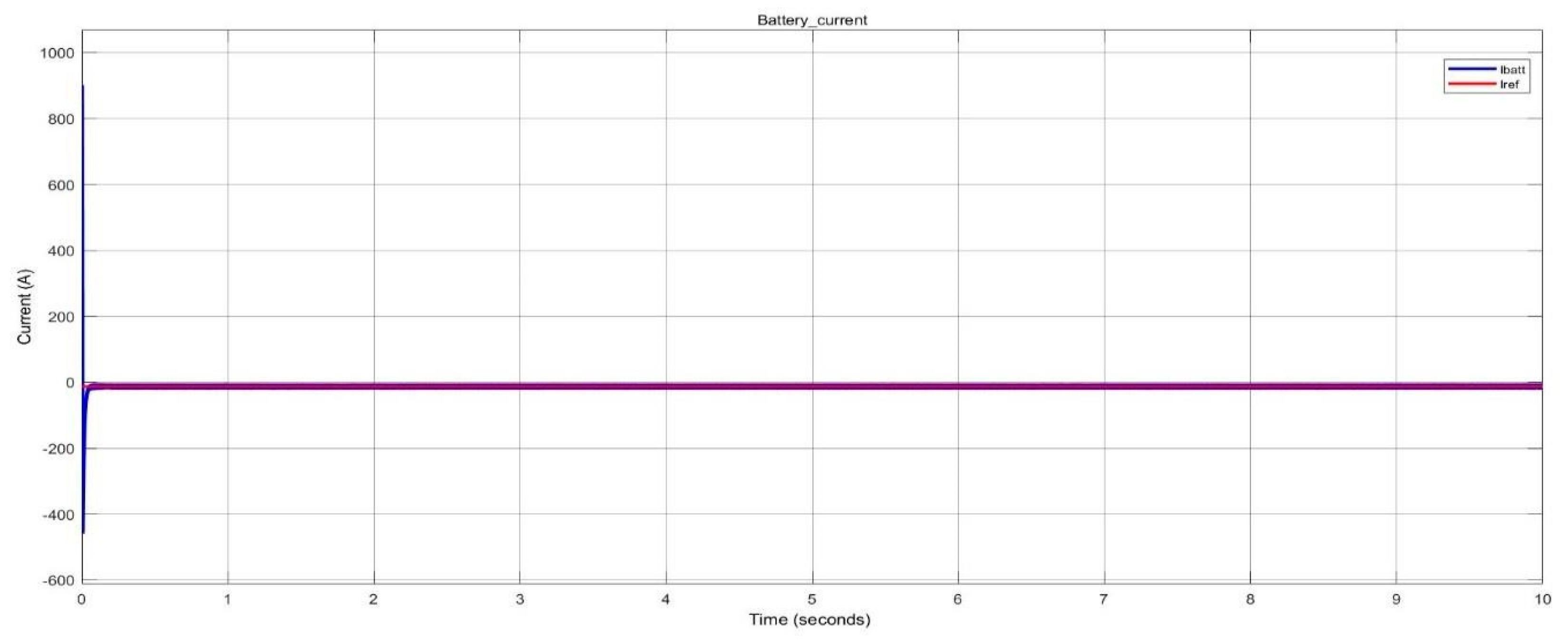
Figure 45.
Battery capacity of BESS during charging in nano-grid system.
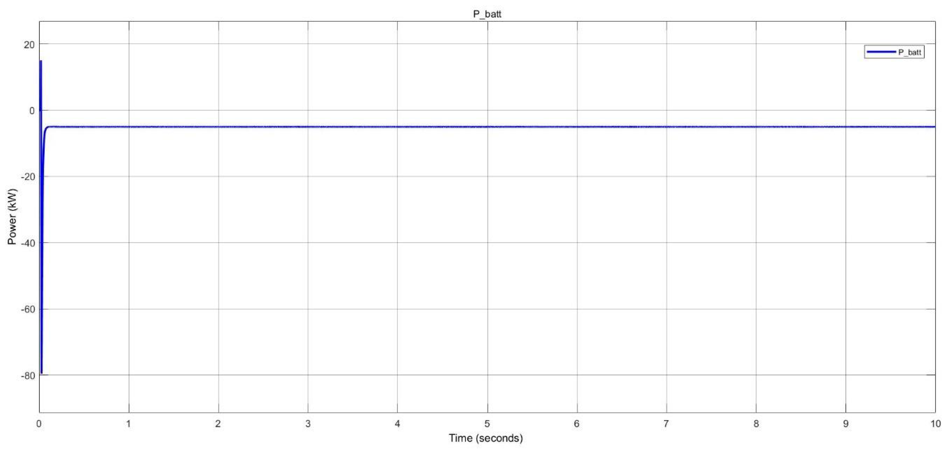
Figure 46.
Drawing power from the grid to charge the battery in nano-grid system.
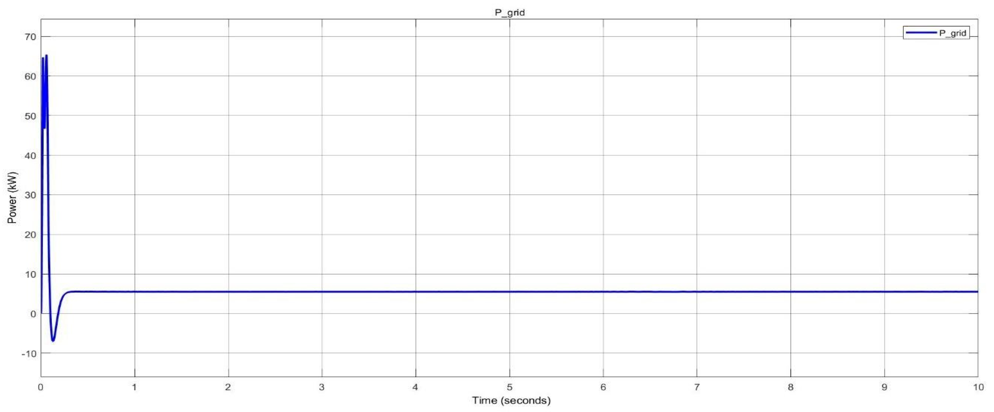
Figure 47.
Simulation model to demonstrate a rainy day operation.
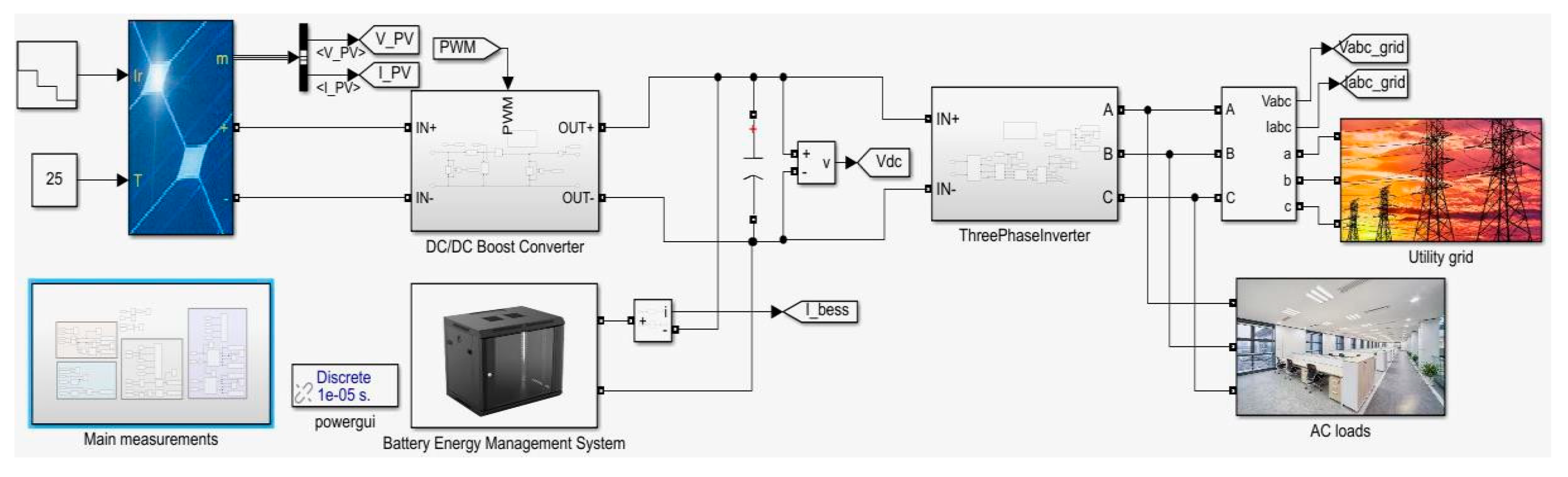
Figure 48.
Load demand estimation of AC loads in nano-grid system.
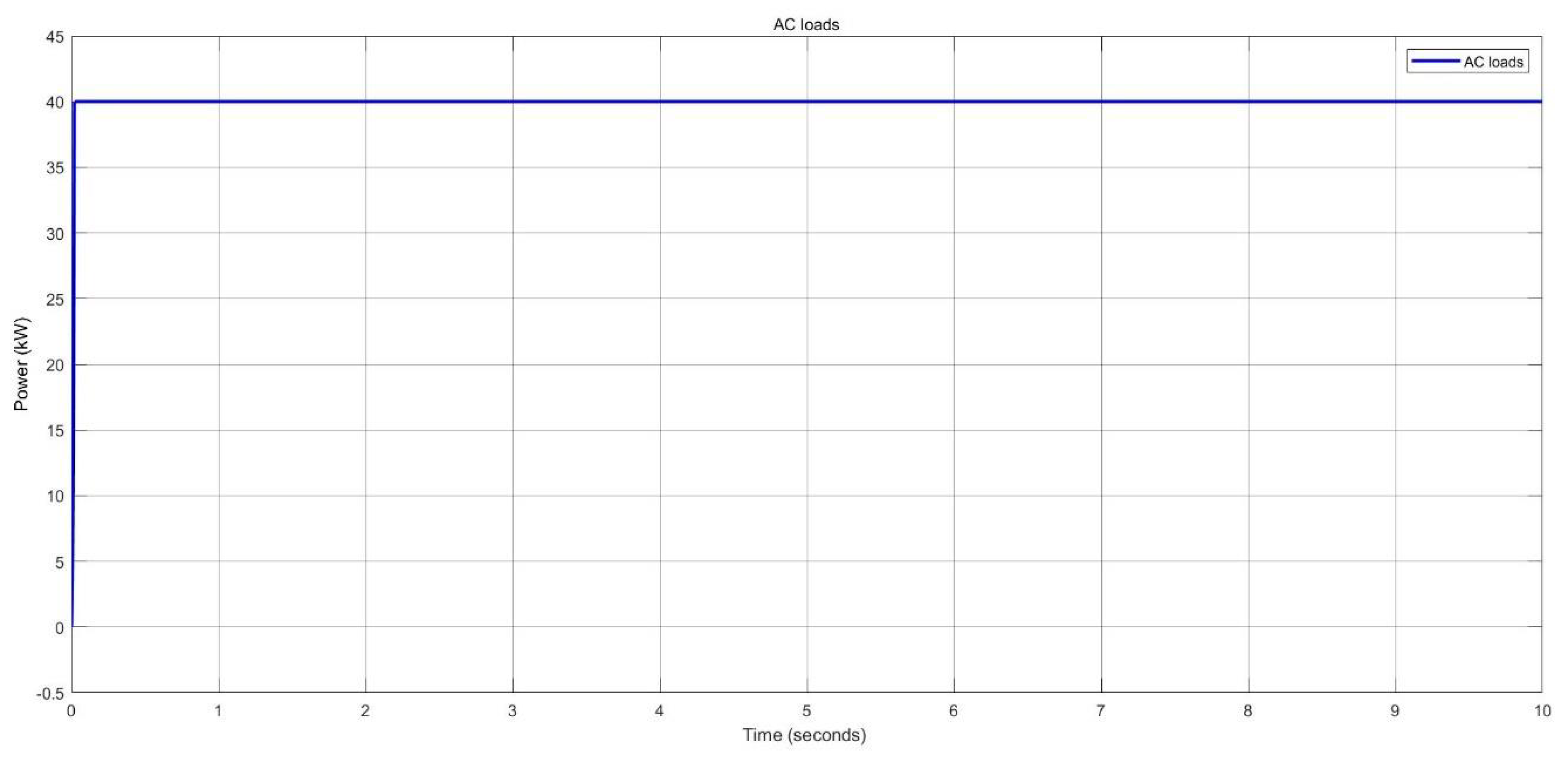
Figure 49.
Solar PV power generated using stair generator in nano-grid system.
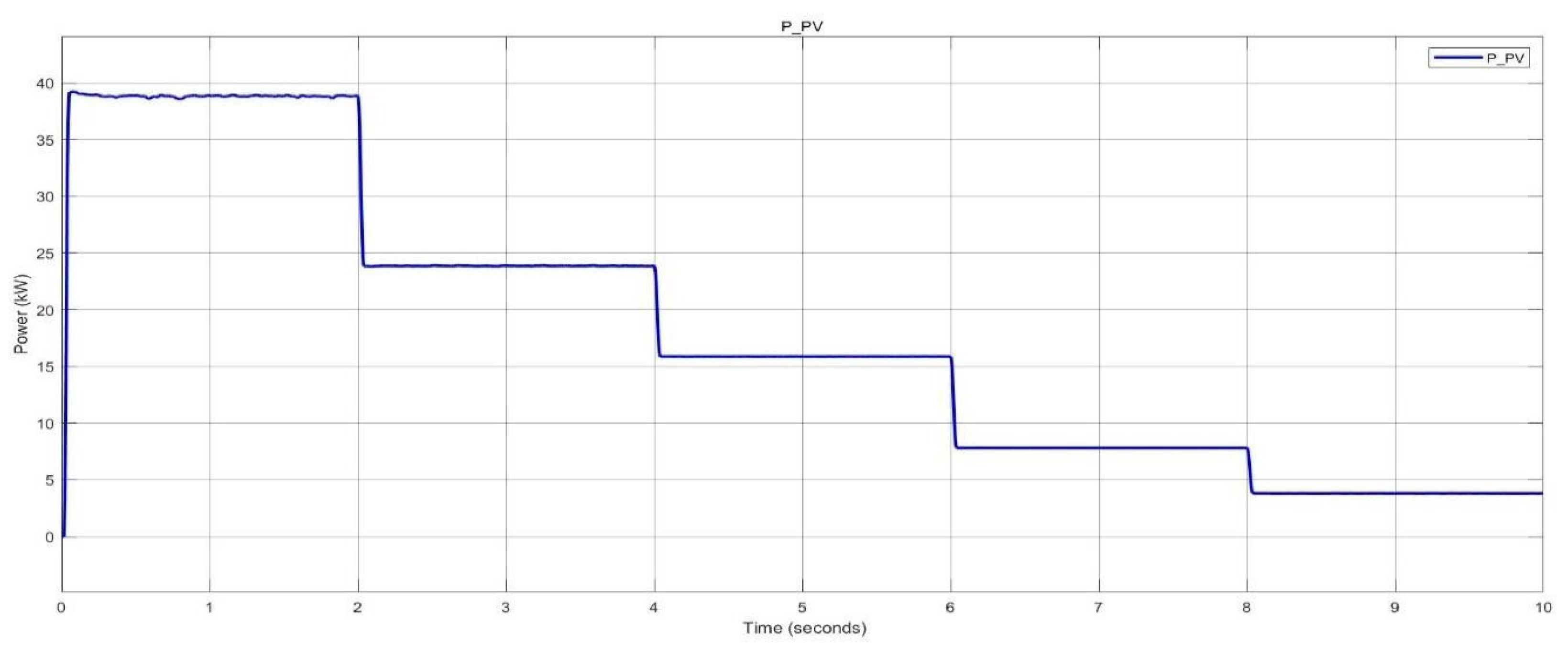
Figure 50.
Power supplied by the grid to the load in nano-grid system.
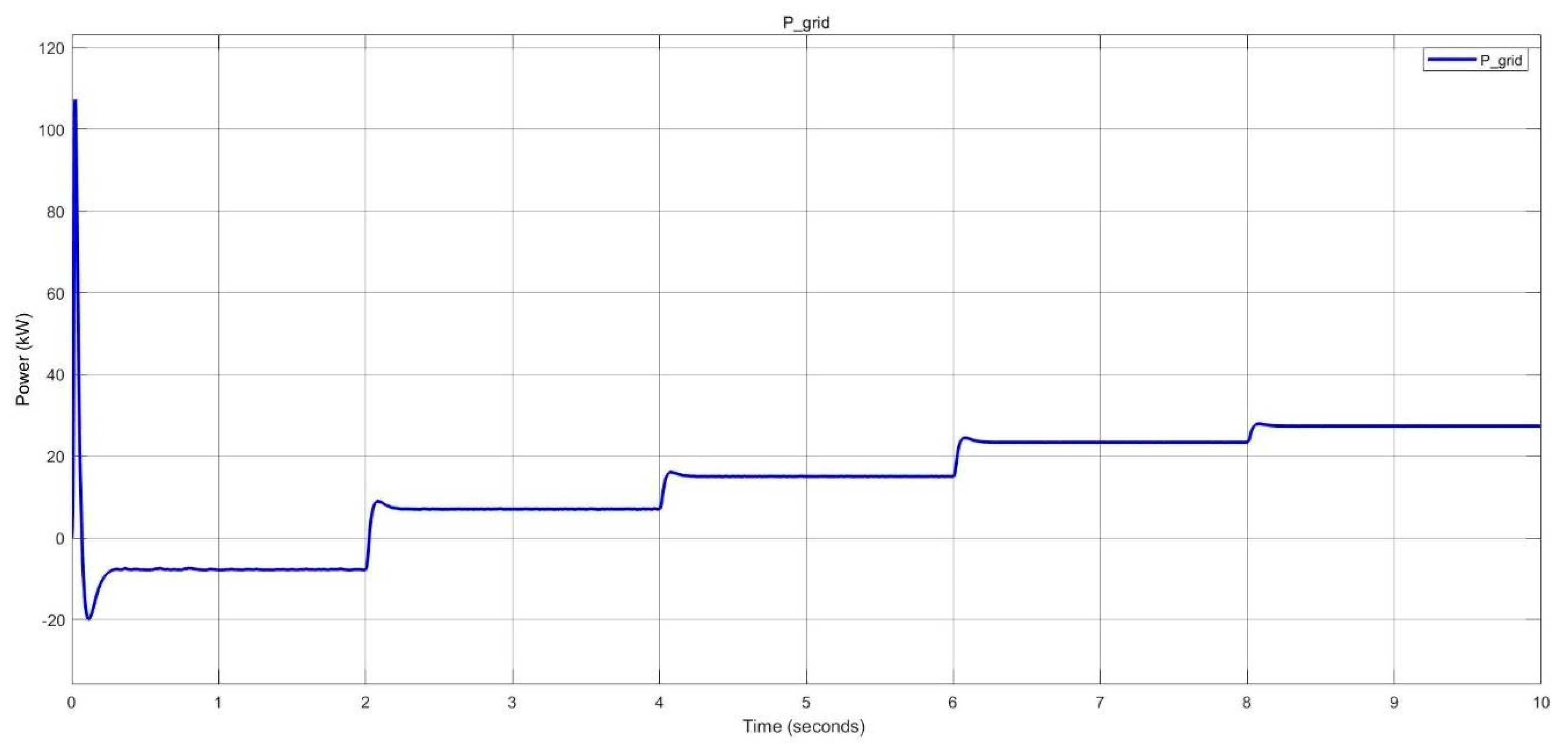
Figure 51.
Simulation model to demonstrate a sunny day operation.
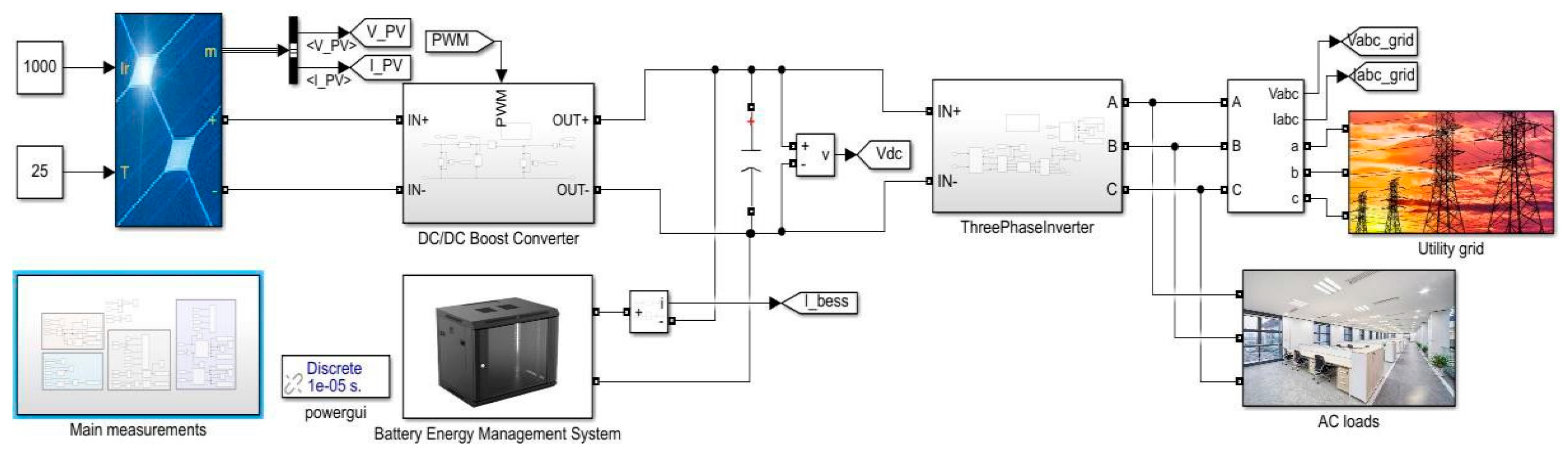
Figure 52.
Load demand estimation of AC loads in nano-grid system.
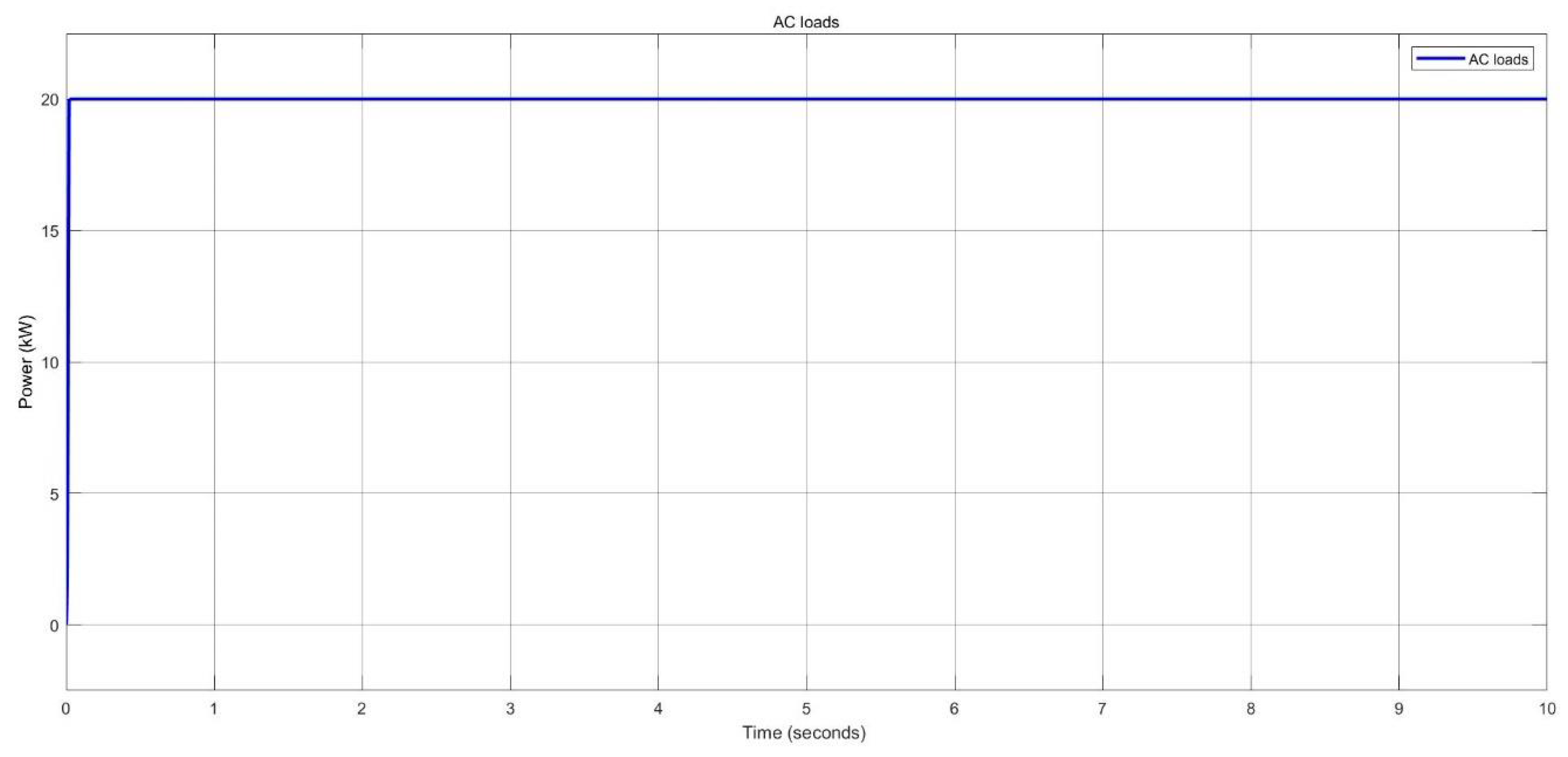
Figure 53.
Solar PV power generated in nano-grid system.
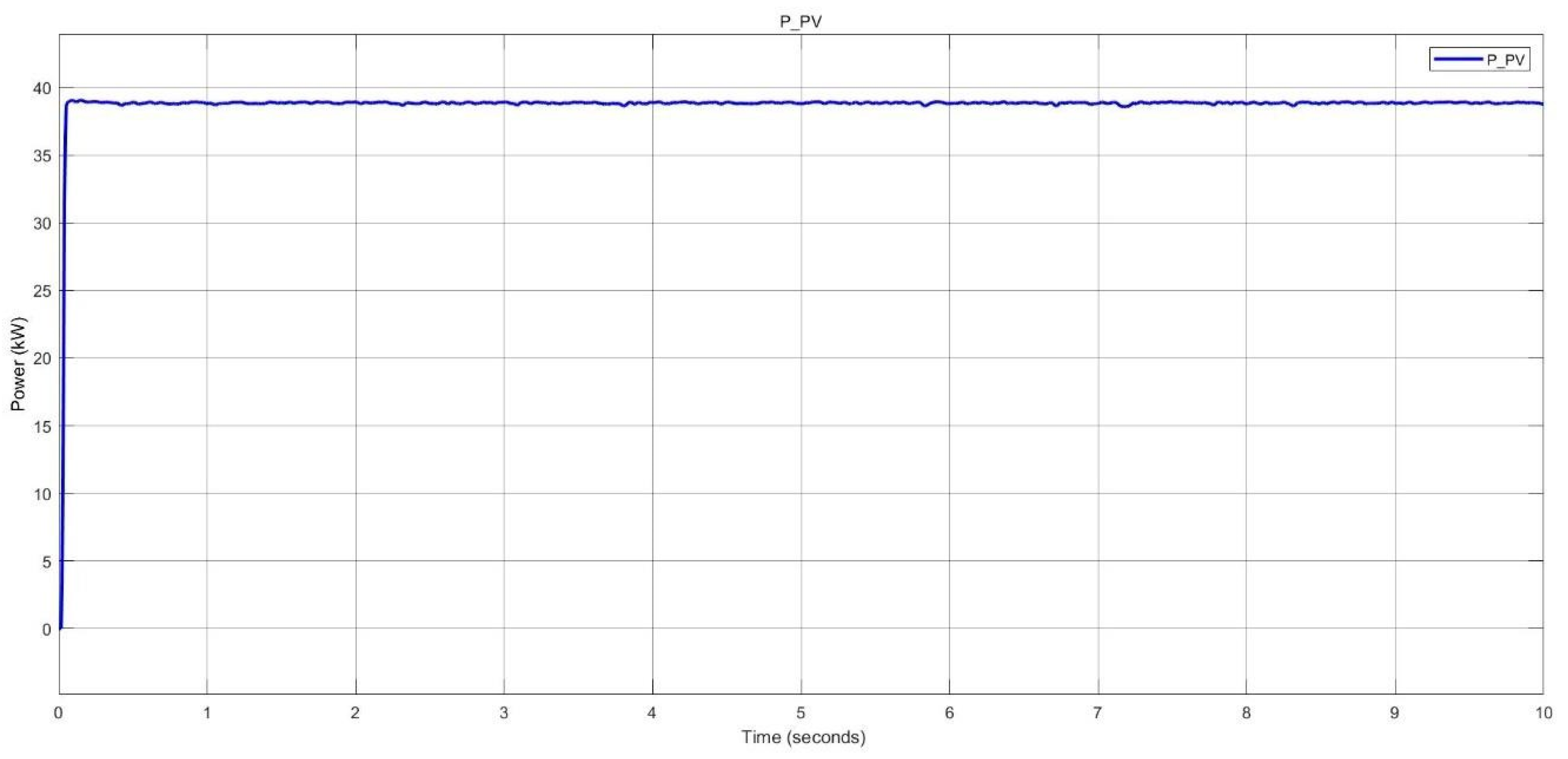
Figure 54.
SOC of battery during charging in nano-grid system.
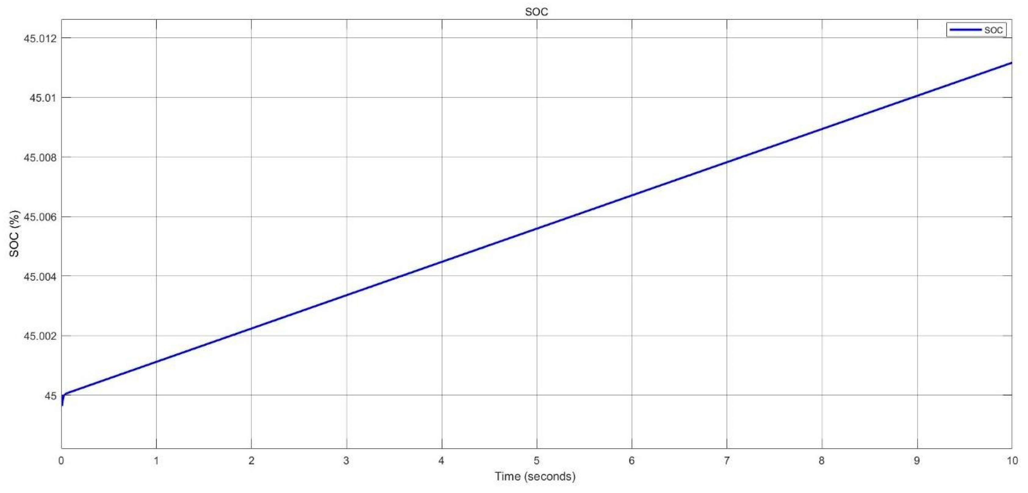
Figure 55.
Battery capacity of BESS during charging in nano-grid system.
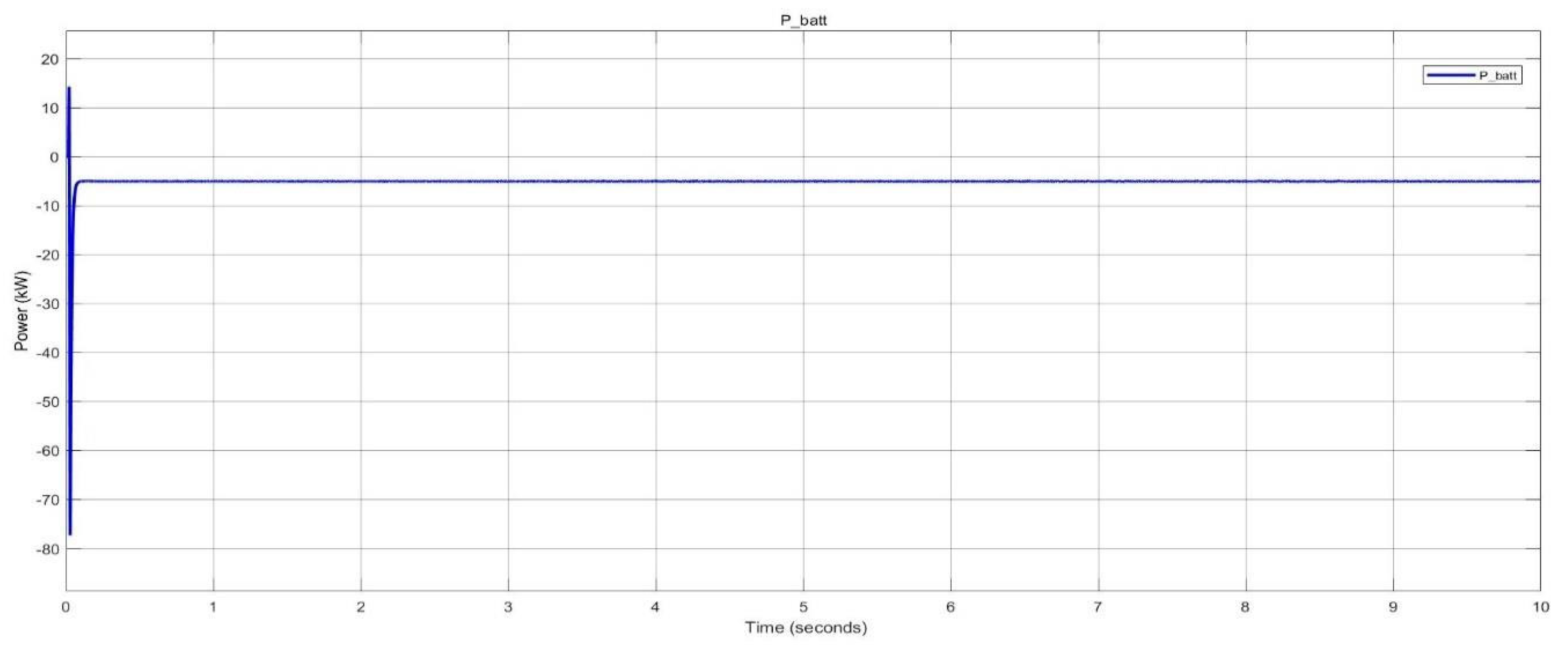
Figure 56.
Surplus power delivered to the grid in nano-grid system.
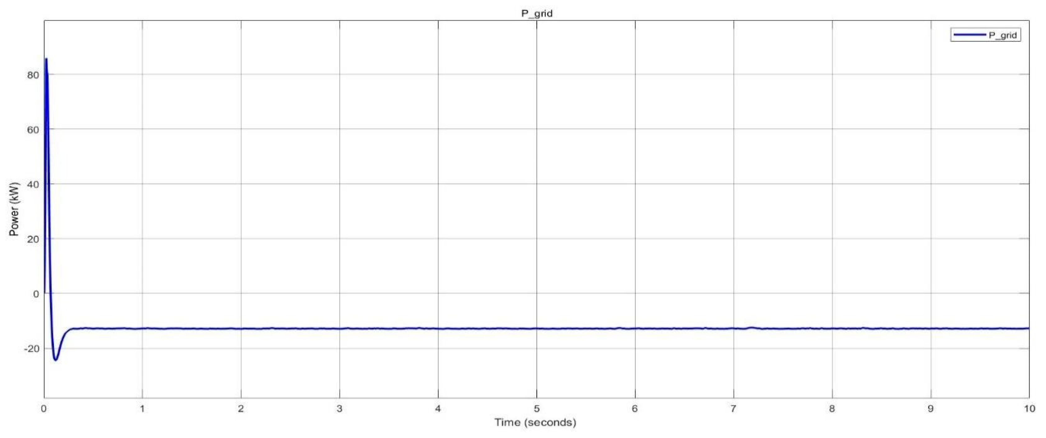
Figure 57.
Two parallel nano-grids connected to the three-phase grid.
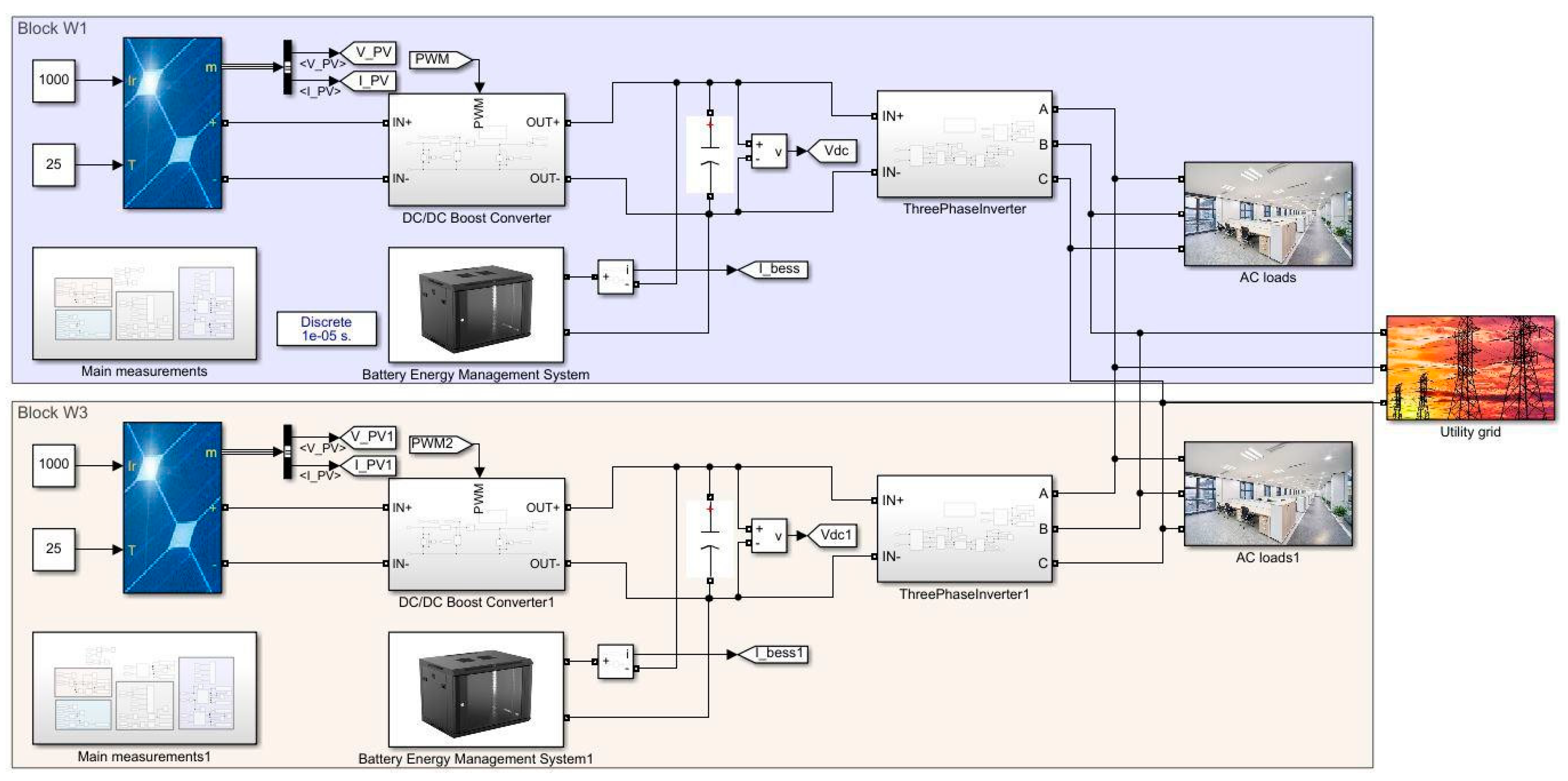
Figure 58.
AC loads before increase for two nano-grids system.
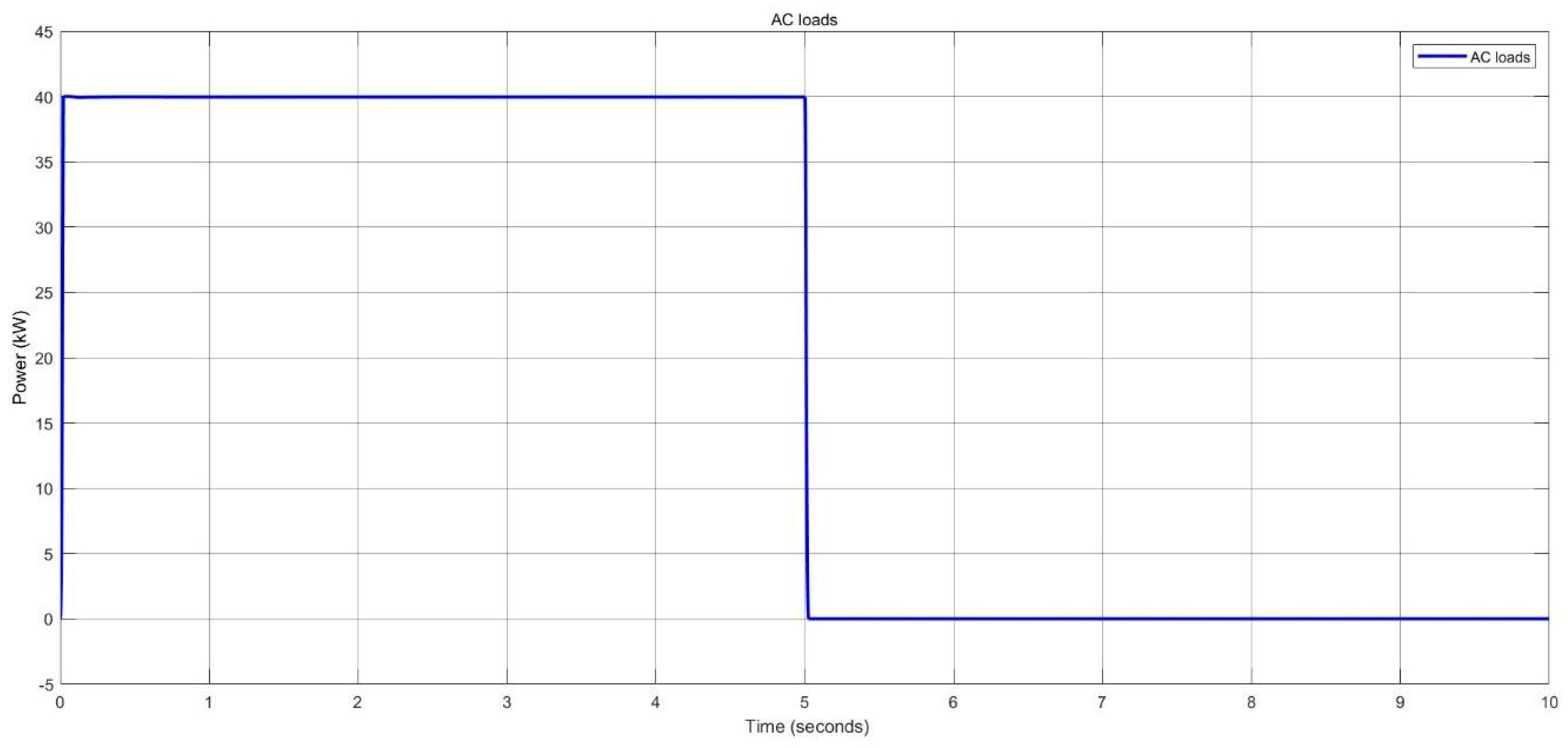
Figure 59.
AC loads after increase for two nano-grids system.
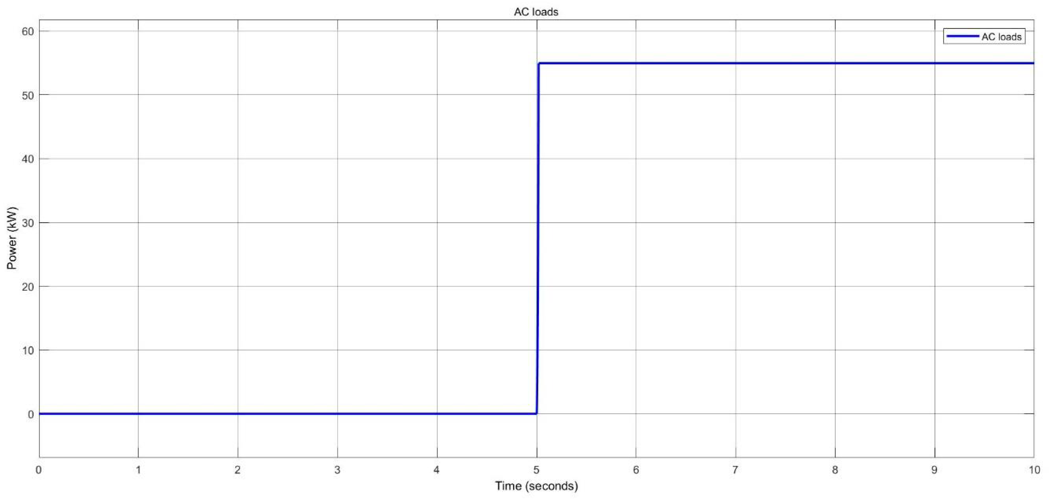
Figure 60.
Surplus power from the system sent to the grid for two nano-grids system.
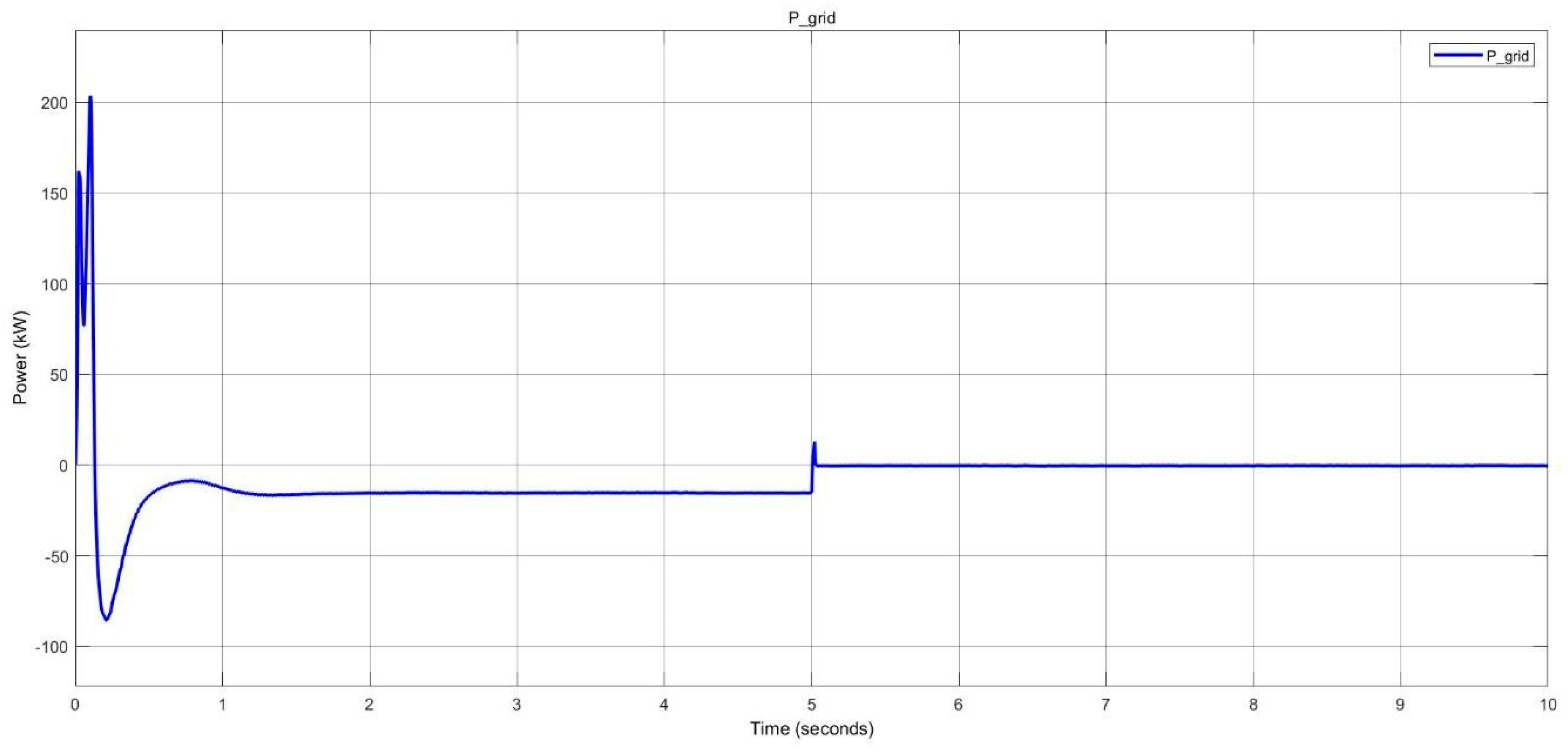

Table 1.
Receptacle loads values for different space.
| Receptacle loads | Nominal values |
|---|---|
| Computer intensive office | 22 W/m2 |
| General office areas | 16 W/m2 |
| Large conference areas | 11 W/m2 |
| Schools (Tertiary/IHLs) | 8 W/m2 |
| Schools (Primary/Secondary) | 5 W/m2 |
| Server/computer rooms | 540 W/m2 |
Table 2.
DC loads estimation of Level B1 to B2 of SIT Punggol Campus.
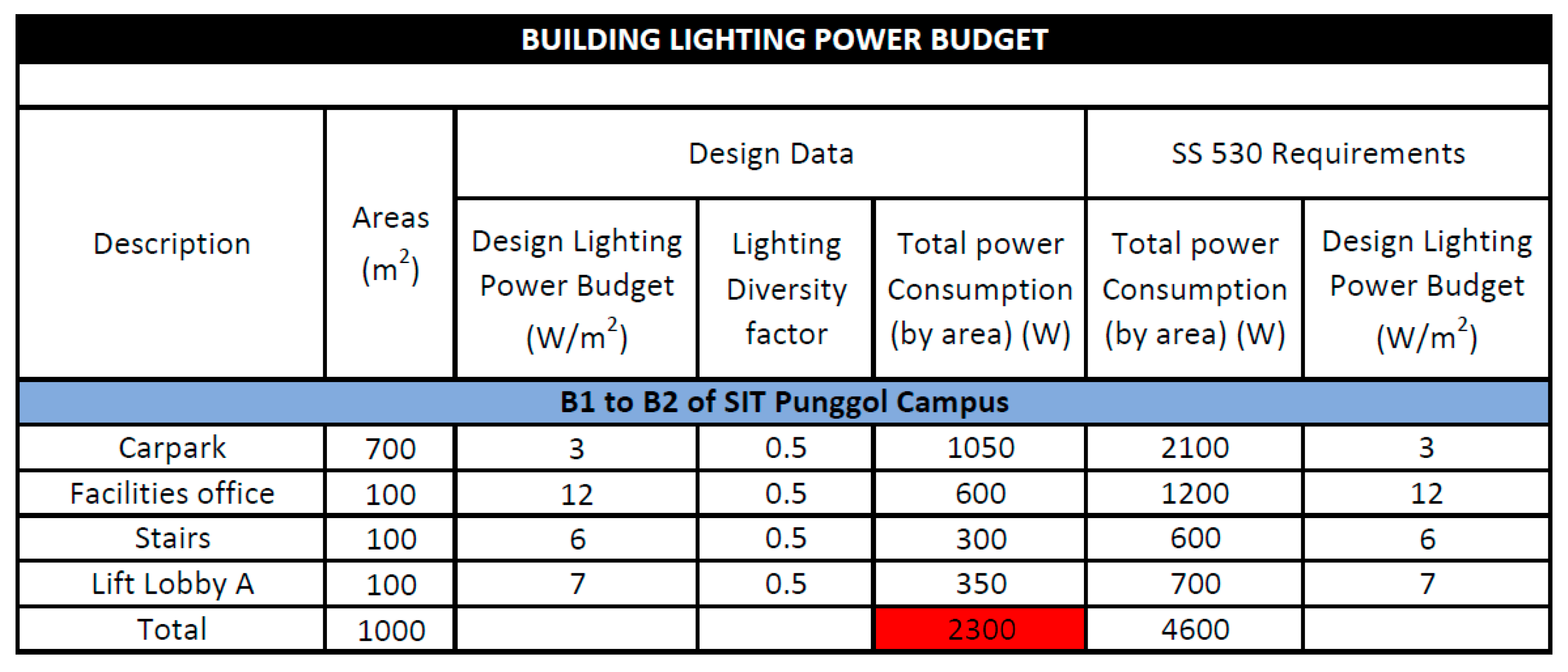
Table 3.
AC loads estimation of Level B1 to B2 of SIT Punggol Campus.
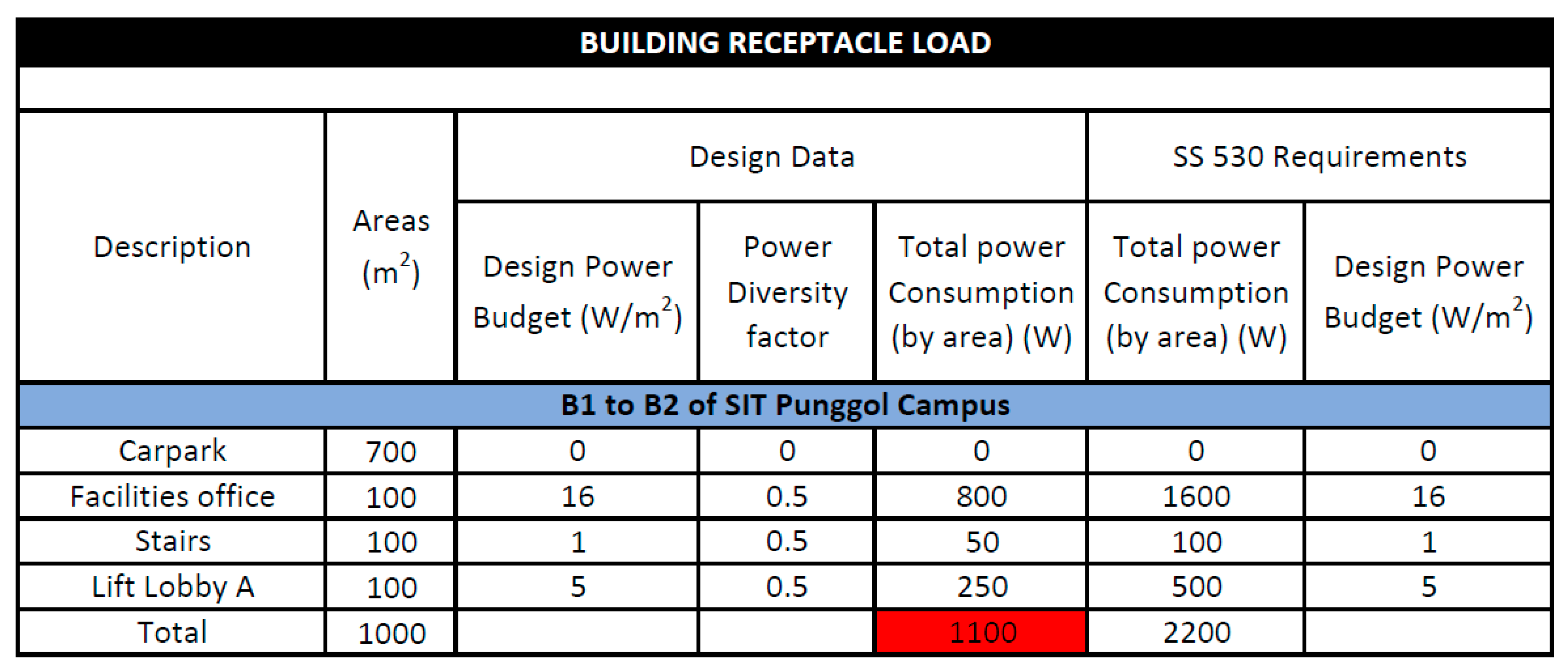
Table 4.
Estimated load demand of Electric Charging Stations for B1 and B2.
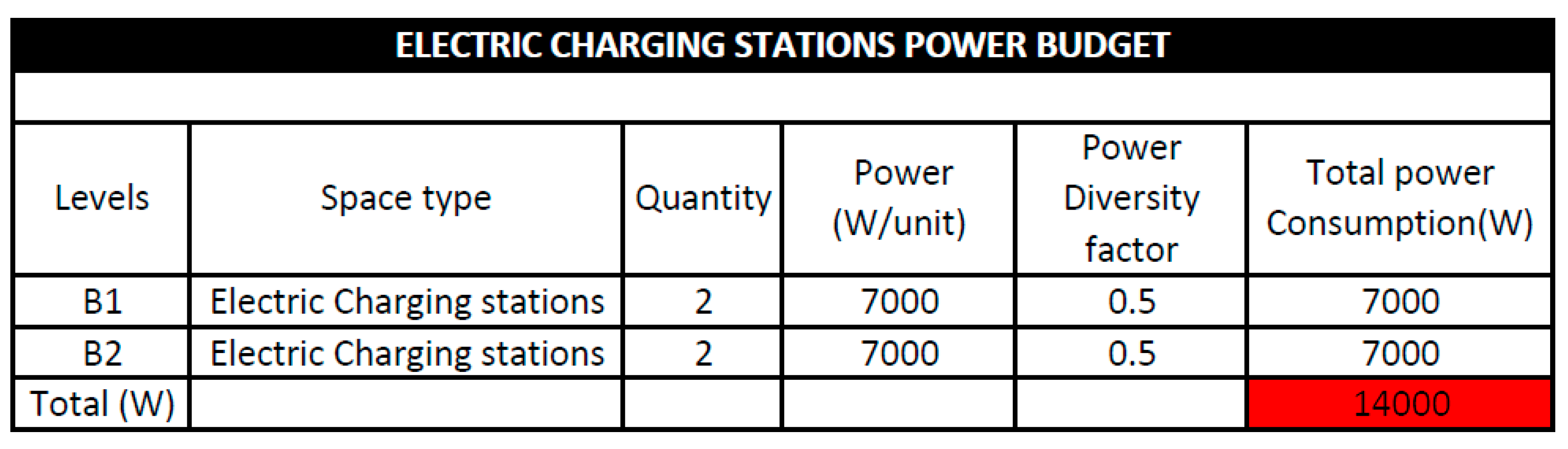
Table 5.
DC loads estimation of Level L1 to L3 of SIT Punggol Campus.
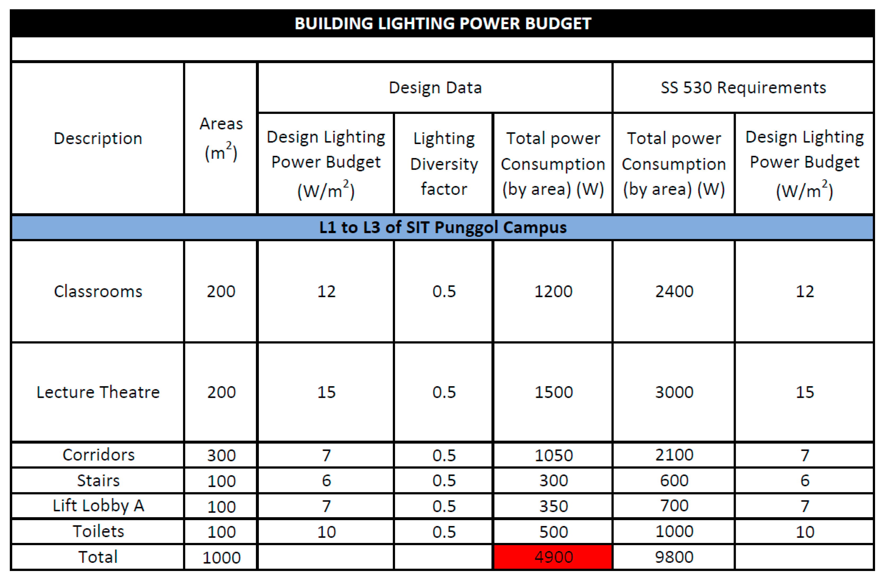
Table 6.
AC loads estimation of Level L1 to L3 of SIT Punggol Campus.
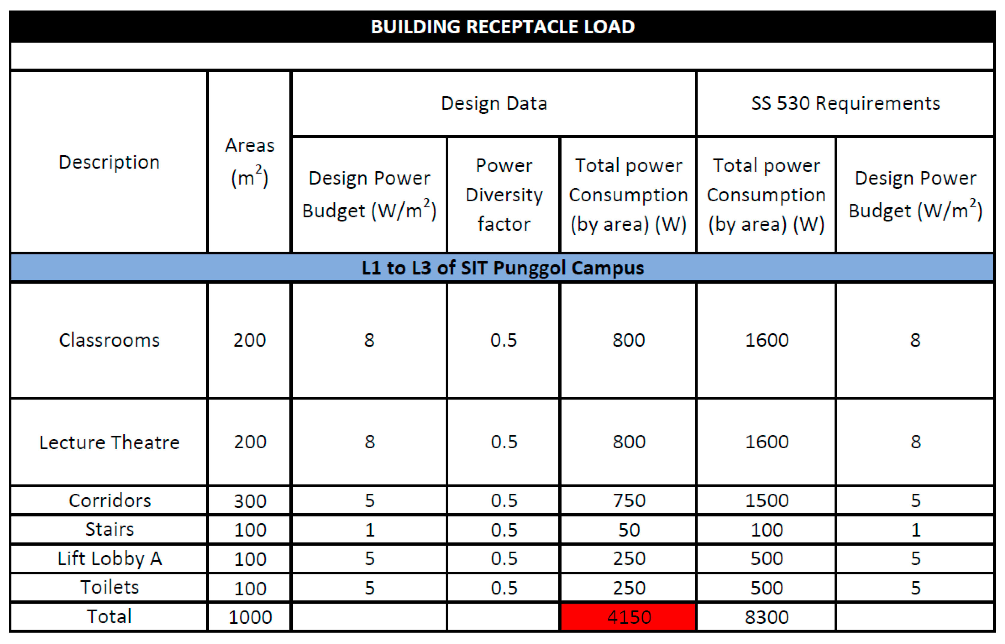
Table 7.
DC loads estimation of Level L4 of SIT Punggol Campus.

Table 8.
AC loads estimation of Level L4 of SIT Punggol Campus.
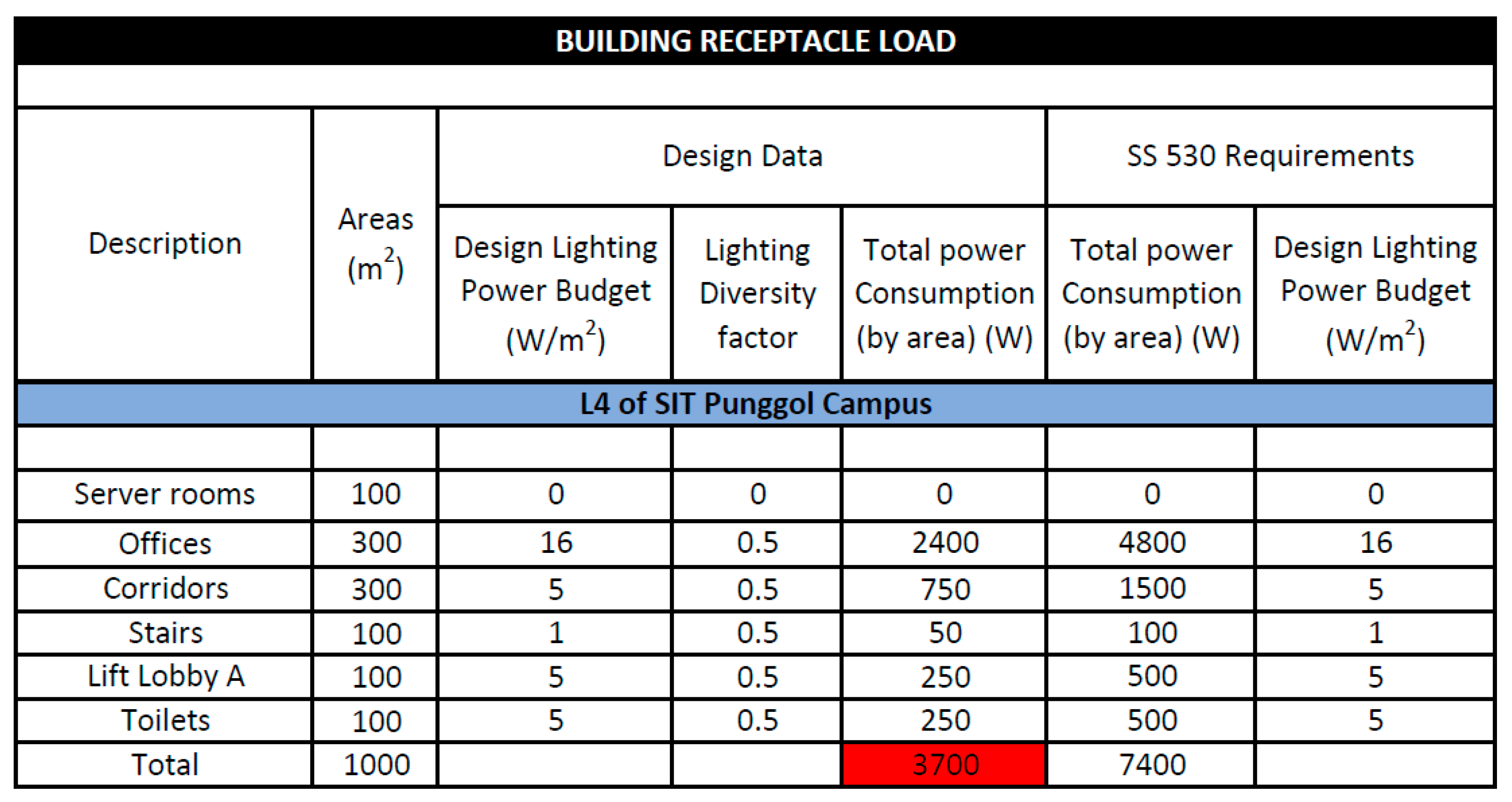
Table 9.
Estimated load demand of server room.
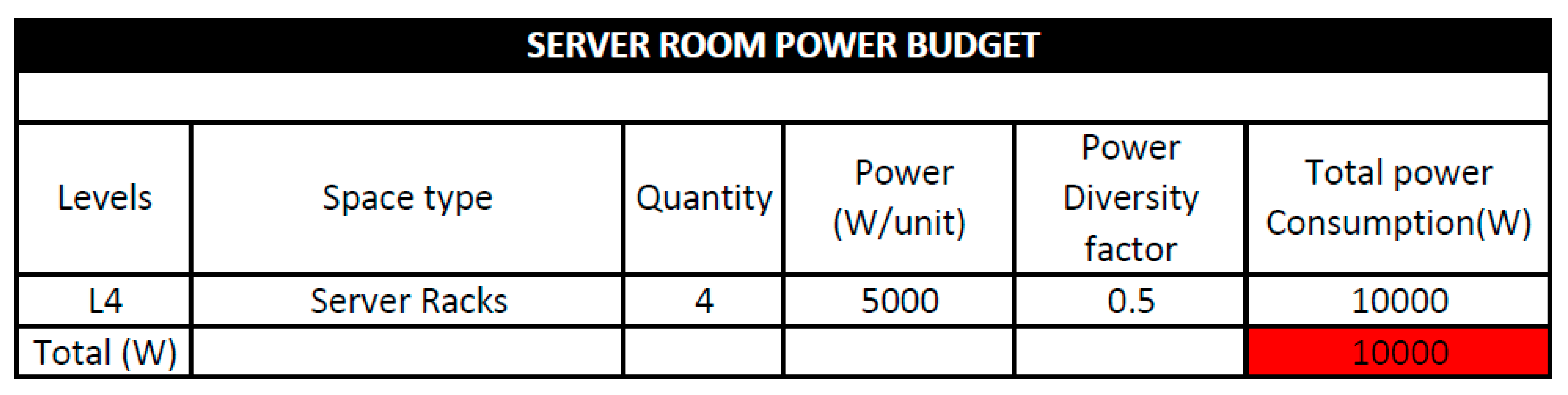
Table 10.
Switching states of the single-phase inverter.
| Cycle | S1 | S2 | S3 | S4 | Voltage at Bridge Output | State |
|---|---|---|---|---|---|---|
| Positive half cycle | ON | OFF | OFF | ON | VDC | 1 |
| OFF | ON | OFF | ON | 0 | 2 | |
| Negative half cycle | OFF | ON | ON | OFF | -VDC | 3 |
| ON | OFF | ON | OFF | 0 | 4 |
Table 11.
Load demand estimation for centralized cooling.
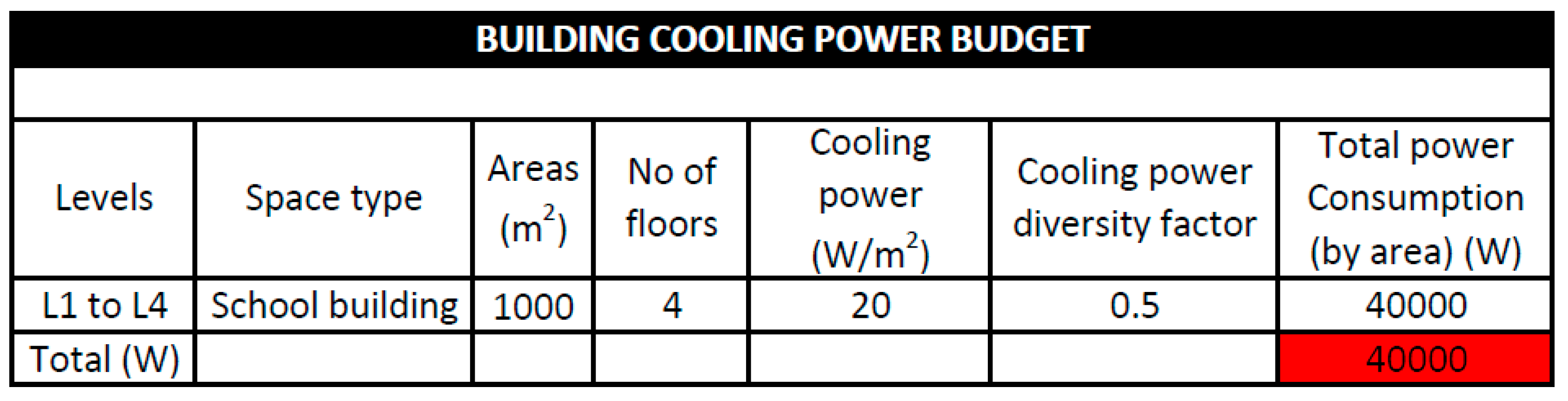
Table 12.
Switching states of the three-phase inverter.
| S1 | S2 | S3 | S4 | S5 | S6 | Vab | Vbc | Vca | State No |
|---|---|---|---|---|---|---|---|---|---|
| ON | OFF | ON | OFF | ON | OFF | 0 | 0 | 0 | 1 |
| OFF | ON | ON | OFF | ON | OFF | -VDC | 0 | VDC | 2 |
| ON | OFF | OFF | ON | ON | OFF | VDC | -VDC | 0 | 3 |
| ON | OFF | ON | OFF | OFF | ON | 0 | VDC | -VDC | 4 |
| ON | ON | OFF | OFF | ON | OFF | 0 | -VDC | VDC | 5 |
| ON | OFF | OFF | ON | OFF | ON | VDC | 0 | -VDC | 6 |
| OFF | ON | ON | OFF | OFF | ON | - VDC | VDC | 0 | 7 |
| OFF | ON | OFF | ON | OFF | ON | 0 | 0 | 0 | 8 |
Table 13.
Parameters of BESS.
| Parameters | Value |
|---|---|
| Battery nominal voltage | Vbatt = 48 V |
| Battery rated capacity | Ibatt = 300 Ah |
| Initial SOC | SOC = 45% |
| Switching frequency | Fsw = 20 kHz |
| Inductor value | L = 5 mH |
Table 14.
Parameters of single-phase inverter.
| Parameters | Value |
|---|---|
| Switching frequency | Fsw = 5 kHz |
| Filter inductor | L = 5 mH |
| Filter capacitor | C = 5 µF |
| DC link voltage | VDC = 400 V |
| Distribution grid voltage | Vgrid = 230 V (phase) |
Table 15.
Parameters of solar PV system.
| Parameters | Value |
|---|---|
| Series connected strings | 10 |
| Parallel connected strings | 10 |
| Vmp | Vmp = 40.8 V |
| Imp | Imp = 9.81 A |
| Sun irradiance | Ir = 1000 W/m2 |
| Cell temperature | T = 25 °C |
Table 16.
Parameters of boost converter.
| Parameters | Value |
|---|---|
| Switching frequency | Fsw = 5kHz |
| Inductor value | L = 2.5 mH |
| Input capacitor value | Cin = 1000 µF |
| Output capacitor value | Cout = 4000 µF |
Table 17.
Parameters of BESS.
| Parameters | Value |
|---|---|
| Battery nominal voltage | Vbatt = 400 V |
| Battery rated capacity | Ibatt = 300 Ah |
| Initial SOC | SOC = 45% |
| Switching frequency | Fsw = 10 kHz |
| Inductor value | L = 1 mH |
Table 18.
Parameters of three phase inverter.
| Parameters | Value |
|---|---|
| Switching frequency | Fsw = 10 kHz |
| Inductor value | L = 10 mH |
| DC link voltage | VDC = 1000 V |
| Distribution grid voltage | Vgrid = 400 V (line) |
Disclaimer/Publisher’s Note: The statements, opinions and data contained in all publications are solely those of the individual author(s) and contributor(s) and not of MDPI and/or the editor(s). MDPI and/or the editor(s) disclaim responsibility for any injury to people or property resulting from any ideas, methods, instructions or products referred to in the content. |
© 2024 by the authors. Licensee MDPI, Basel, Switzerland. This article is an open access article distributed under the terms and conditions of the Creative Commons Attribution (CC BY) license (http://creativecommons.org/licenses/by/4.0/).
Copyright: This open access article is published under a Creative Commons CC BY 4.0 license, which permit the free download, distribution, and reuse, provided that the author and preprint are cited in any reuse.


