
Submitted:
26 June 2024
Posted:
27 June 2024
You are already at the latest version
Abstract
This paper presents a hybrid modelling approach that combines physics-based electromigration modelling (PEM) and statistical methods to evaluate the electromigration (EM) limits of nano-interconnects in mesh networks. The approach, which is also compatible with standard Place and Route (P&R) tools and practices, takes into account the positive impact of network redundancy on EM current limits. The study shows that conventional methods underestimate the EM current limits of a power delivery network (PDN) unit-cell by 80% due to their lack of consideration for redundancy. Additionally, the time-to-failure (TTF) distributions of a PDN unit-cell adhered to a lognormal distribution, where the lognormal sigma, σlogn, exhibits a 55% reduction compared to that of the single constituent interconnects. The study also found the negative voltage (i.e. ground or Vss) grid to be more susceptible to EM than the positive voltage, i.e. Vdd grid. In the examined grid unit-cell design, both the number of interconnect sites prone to voiding and also the magnitude of the peak tensile stress within the nano-interconnects were found to be 2-folds as high in the Vss case compared to Vdd. lognormal sigma of TFF for the grid unit-cells, σ_(logn-tile), show a marked reduction compared to the lognormal sigma of the constituent single interconnects, σ_logn, with a 50% and 66% decrease compared to single interconnects, for downstream (Vss) and upstream (Vdd), respectively. In addition, σ_(logn-tile) was 3-folds higher for downstream (Vss) compared to upstream (Vdd), whilst, in contrast this difference was only 2-folds at single interconnect level. 4.13-folds higher TTF50% was observed at grid unit-cell level for upstream compared to downstream operation which was also more pronounced than in the single interconnect level where the difference was only 2-folds. This research provides valuable insights into EM aging of nano-interconnects in mesh networks and could pragmatically enhance the accuracy of EM compliance evaluation methods.
Keywords:
Nano-Interconnects
; Reliability
; Electromigration (EM)
; Redundancy
; Mesh Networks
; Power Delivery Network
; Physics-Based Modelling
; Statistical Electromigration Budgeting (SEB)
; Tile-Based SEB.
1. Introduction
The rapid integration of electronics into daily applications, such as the automotive industry and the Internet of Things (IoT), underscores the need for research and innovation in design-for-reliability paradigms more than ever. In the realm of Very Large Scale Integration (VLSI) reliability, the use of overly conservative approaches, which involve large reliability margins and safety factors, restricts the design space, thereby affecting chip performance and power consumption. Given the anticipated computing energy demands associated with the rise and prevalence of artificial intelligence (AI) [1], along with the complexity implications of materials and manufacturing processes, these overly pessimistic reliability paradigms are at odds with global sustainability requirements and the sustainability obligations of the semiconductor sector.
One of the key (VLSI) reliability challenges concerning metal interconnections is electromigration (EM). EM is a phenomenon where metal atoms are displaced due to the momentum transfer from conducting electrons [2,3]. This displacement can lead to the formation of voids in interconnects, causing circuit failures. The failure is by void nucleation and growth at the cathode end of interconnects which results in an increase of interconnect resistance impairing circuit operation. For instance, it can induce timing errors and eventually lead to open circuit failures. The impact of EM on the reliability of VLSI circuits has been a topic of extensive research as a central interconnect reliability concern [4,5].
In standard EM tests, interconnects are characterized by determining their time-to-failure (TTF) under constant direct current (DC) tests with flux divergence points at their two ends. An interconnect is considered to have failed when its resistance increases beyond a target value, often 10% resistance shift (R-Shift). Tests are conducted at accelerated conditions by increasing the current density and temperatures. Multiple interconnects are tested under different temperatures and current conditions and the mean-time-to-failures (MTTF) at different conditions are used to determine the activation energy, Ea and the current density exponent, n, of the Black’s equation [2,6,7,8]. TTFs follow a lognormal distribution, whereas the lognormal and Black’s equation parameters are used to derive an EM current density limit, jmax, for a target EM failure probability and lifetime [9,10]. The current density limit, jmax, is usually reported in the process design kits (PDKs) provided by the foundry to be employed by the designer for EM compliance checks in the Place and Route (P&R) phase.
Fundamentally speaking, EM is correlated with the cohesive energy of metals and therefore also correlated to their meting point. Many widely used metals in CMOS technology such as Al and Cu suffer from EM. In contrast, for metals with high melting temperature such as Ru, Mo and W, EM is not a major reliability concern [11,12]. Many material and process-related factors are implicated in EM, including interfacial properties e.g. adhesion [13], Cu microstructure (i.e. grain size distribution) [14,15,16,17,18,19], mechanical and fracture properties of the metal, confining materials and dielectrics and residual stresses [20,21,22,23,24,25,26]. Thereby, technological solutions involve material and process innovations such as using dopants (e.g. AL and Mn) that segregate into Cu grain boundaries and also implementation of liners and metal capping e.g. Co cap [27,28,29], each with their pros and cons in terms of resistivity and cost [30,31].
With increase of current densities and drastic decline of EM robustness due to miniaturization of interconnects [16,32,33,34], EM is considered to be a significant reliability challenge for the ongoing scaling [35]. As scaling progresses, delay shifts attributed to EM are anticipated to overshadow other aging mechanisms such as hot carrier injection (HCI) and bias temperature instability (BTI) [36]. Despite the advent of EM-robust alternative metals such as Mo, Ru projected for used in angstrom nodes [11,12], resistivity considerations restrict their application to wires narrower than ~12 nm linewidths [37]. Thus, the back-end-of-line (BEOL) will continue to display a hierarchical architecture where wider metal levels will be Cu-based given its cost and resistivity benefits [37]. Moreover, the rise of back-side power delivery networks (BS-PDNs), where the PDN is processed on the opposite side of the wafer [38,39], justifies the use of Cu in back-side power delivery applications given available spacing for more relaxed linewidths. In this scenario, transistor heat generation and interconnect joule heating in the absence of effective chip cooling options [40], will raise Cu interconnect temperatures and temperature gradients, thereby intensifying EM aging [41,42]. Evidently, EM will persist to be a reliability concern as we venture into the angstrom technology era.
The standard design-for-reliability approaches widely employed for EM by the industry are; (i) the limit-based approach (LBA) which predicts system failure when the average DC current density, j, exceeds jmax, for any interconnect, ignoring the statistical nature of EM [43,44] and, (ii) the statistical EM budgeting (SEB) which employs the weakest link statistics considering the distribution of j/jmax ratio of all single interconnects [43,44]. Thereby in these methods, failure is predicted when jmax is violated in any single interconnect or the failure probability is predicted based on a first-to-fail interconnect criterion, respectively. This assumption is plausible for circuits where interconnects are connected in series. However, the PDN, which is most prone to EM because of high average magnitudes of unipolar currents, has a grid-like architecture with many parallel interconnect paths. Thereby, if one interconnect suffers from EM, the current will be redirected to redundant parallel paths. Clearly, application of the conventional EM compliance evaluation methods to PDN may be overly pessimistic, as formation of the first void alone doesn’t necessarily cause a system failure [45].
To this end, many studies have been dedicated to investigation of EM in grid-like networks using both experimental and simulative approaches. Zhou et al. (2018), used a test chip to study EM effects in PDNs, and observed mechanical stress-dependent failure locations in grids and self-healing due to redundant current paths [46]. Using a similar on-chip approach, Pande et al. (2019), captured several EM effects ranging from abrupt and/or progressive failures, temporary healing effects and circuit-interconnect interplay, which may not be observed by single interconnect characterization [47]. Lin et al, conducted systematic experiments on the impact of redundancy by using test structures with different number of parallel interconnects, and proposed a statistical model to predict the TTF of parallel interconnect networks based on the TTF of the last failing interconnect [48]. As the latter model was purely statistical, the physical dynamics, e.g. current redirection and accelerated aging of the late failing interconnects, could not be captured. Yet the approach, explained many of the key EM characteristic trends of parallel systems such as the decrease of lognormal sigma, , with increase of redundancy [48]. With increasing complexity of grid architecture, however, their model predictions diverged from experimental findings, possibly due to neglecting the time-dependent physical cascade of phenomena such as current and stress redistribution within the grids. In this context, understanding of the distribution of EM induced hydrostatic stress within the grid, has been shown to be the pre-requisite to determine the EM failure locations [49]. EM voids occur in locations of high tensile stress which don’t strictly coincide with locations of peak current within a grid and requires grid-level stress analysis [49]. To this end, physics-based modelling of EM has seen significant advances in recent years considering transient simulation of all stages of EM aging where models have become more technology and microstructure aware [50,51,52,53,54,55,56,57,58,59,60,61]. However, application of such exhaustive models to grids with billions of segments entails significant computational costs. Mainly because, simulation of post-voiding cascade of events requires transient coupled electrical-EM analysis to capture current redistribution within the grid. To minimize such computational costs, model order reduction together with filtering algorithms that confine the analysis to critical interconnect segments have been adopted in the literature [62,63,64,65]. Furthermore, due to their computational expense, complexity, and parametric uncertainty, the statistical aspect of EM is frequently overlooked. This often results in models failing to deliver the crucial chip-level failure probability. In addition to the need for electronic design automation (EDA) software packages capable of resolving transient mechanical stress distribution across the entire chip before and after void-nucleation, the adoption of stress-based approaches necessitates the provision of mechanical stress limits (i.e. critical stress) from the foundry. These limits can only be indirectly inferred, for instance, through model-based approaches. Therefore, despite their inherent limitations, current-based EM compliance evaluation methods continue to be the industrial benchmark.
To overcome the described practical constraints and account for grid redundancy in chip-level reliability predictions, we recently introduced the concept of a PDN-tile-based EM compliance check, see Figure 1. This method derives current limits for the unit cells (or tiles) of the PDN. This approach is practical because PDNs are architecturally composed of repeating grid unit-cells, each consisting of parallel interconnect paths. Consequently, the redundancy impact is inherently captured in the current limits determined at the tile level characterization. Further, tile-based SEB would be applied, where PDN tiles are considered as the fundamental elements for weakest link statistics, instead of single interconnects, see Figure 1. This allows for scalable EM assessment of PDNs, considering the impact of PDN redundancy [66].
In this paper, the proposed tile-based concept is expanded by outlining a physics-based simulation modeling framework for PDN unit cells. This framework can predict their EM current limits using a Monte-Carlo approach. We present a calibration methodology for the model using standard EM test data, considering uncertainty propagation in the pre-nucleation and post-nucleation phases. A stress-based analysis predicts the EM failure locations within the PDN tile, taking into account the stochastic nature of void nucleation. The fundamental differences between EM in the negative supply voltage, Vss grid and the positive supply voltage, Vdd grid are investigated. In addition to pre-nucleation stress evaluation and void nucleation, the post-voiding EM aging phase and the variability induced by the stochasticity of void dynamics are efficiently simulated. We achieve this by using an order-reduced void impact model that can be calibrated directly from standard EM experimental data. The developed simulation framework is validated using experimental data on the impact of redundancy. Subsequently, the modelling framework is used to predict the EM behavior of a realistic PDN unit-cell, determining the impact of redundancy on EM failure probability and tile-based current limits.
2. Method and Materials
2.1. Network-Aware Modelling Framework
A network-aware EM modelling framework was devised and developed by coupling a circuit solver module with a Korhonen-type [50] EM modelling module. The electrical current in each interconnect segment of the network was derived using the circuit solver and communicated to a 1D partial differential equation solver which solved the Korhonen EM model over each interconnect to determine evolution and distribution of hydrostatic stress along its segments. Once a critical tensile stress was reached at a location along the interconnects, void nucleation was considered and a compact resistance evolution model determined the increase of interconnect segment’s electrical resistance. The resistance increase was considered in the subsequent simulation time step to determine current redistribution through the network due to EM voids. In terms of numerical implementation, the electrical circuit solver module and the EM solver module were coupled by sharing log files in every time step of an explicit solution approach. The minimum stable time-step was determined through sensitivity analyses. The simulation framework was implemented within Matlab® environment using Simscape in Simulink for electrical circuit analyses and the PDEPE partial differential equation solver for the solution of the Korhonen-type EM model, where, the communication and coupling of the modules were conducted using custom-developed programs.
The electrical circuit was modelled as a resistive network, where, the resistance of each line segment, each via and their connectivity were pre-assigned per interconnect design and technology assumptions. The operation of the circuit was simulated under an ideal current source which represented the testing stress current or the current from standard cells, where the circuit operated under upstream (US) or downstream (DS) conditions, by changing the direction of the ideal current source. The algorithmic diagram is demonstrated in Figure 2.
2.2. Electromigration Model
During EM, the electron wind force depletes the ions in the direction of the electron flow while a back stress develops and drives ions in the opposite direction, so that [50]:
where, represents the flux of Cu ions, is the diffusivity, is the concentration, is Boltzmann’s constant, is temperature, is the effective charge number, is the fundamental electronic charge, is the electric field where
is the resistivity of Cu, is the current density, is the atomic volume, and is the hydrostatic stress gradient along the line.
Self-diffusion takes place within the boundaries of each interconnect domain as confined by the dielectric and metallic diffusion barriers used in the damascene technology. In this context, diffusion barriers block Cu self-diffusion across the interconnect boundaries, whereas, self-diffusion dominantly takes place along Cu interfaces and grain boundaries [15]. Therefore, EM was modelled within interconnect domains isolated by the diffusion barriers, separately. Such domains, may be composed of multiple segments with distinct electrical currents.
Electromigration aging can be subdivided into two main phases; (i) the pre-nucleation phase, where tensile stress builds up at the cathode end of interconnects until a critical stress required for void nucleation is reached and (ii) the post-nucleation phase, where the nucleated voids enlarge and evolve, increasing interconnect resistance.
Considering the mass balance equation and using equation 1, Korhonen derived a 1D partial differential equation (PDE) that describes the evolution of hydrostatic stress, , along an interconnect during EM [50]:
where, is the effective elastic bulk modulus of the interconnect determined by considering the impact of confining layers and the dominant diffusion paths, i.e. interfaces and the grain microstructure of the metal [24].
The physical input parameters for the EM model depend on interconnect dimensions, the type of dielectrics, and the barrier/liner/capping schemes [33]. The line width-dependent values of these parameters were previously reported in [33] and were employed in this study as summarized in Table 1.
The fluxes at the two ends of the 1D electromigration domains are zero given the blockage by the diffusion barriers. Thus, by equating the total flux in equation (1) to zero at the two ends, i.e. , at x=0 and x=L, the stress boundary condition for the solution of equation 2 is derived as follows:
The initial stress was simplified and considered to be constant along the domain where technology relevant values as in [1] were applied, see Table 1.
Once the EM-induced tensile stress calculated by the stress evolution PDE reached a critical stress, , a void was considered to nucleate in the location, and a growth phase was initiated. Upon void nucleation, the stress at void surface relaxes to zero to ensure continuity of chemical potential energy [60]. This relaxation generates large stress gradients adjacent to the void surface which drives diffusion from the void up the stress gradient resulting in increase of void volume. Korhonen suggested use of a post-nucleation boundary condition at the cathode end of the interconnects, assuming that the void is exactly at the cathode end, to capture the flux of atoms from the void surface as follows [50]:
where , is the width of the interconnect, assuming that the peak stress at void relaxes to zero over a characteristic length equal to the width of interconnect to estimate the stress gradient that drives atoms away from the void surface through fast diffusion paths. Application of this boundary condition for the solution of equation (2) post-nucleation can capture stress relaxation starting from the cathode void and propagation to the rest of interconnect resulting in a shift of stress towards compression in the rest of the interconnect. In this case, the void volume at any time can be derived as follows [67]:
where, A is the cross-sectional area, L is length. In high temperature accelerated tests on long interconnects, the void growth rate before volume saturation can be approximated as a function of the electron current density where the longitudinal drift velocity of an incubated void is [15]:
Assuming Cu and the (combination of barrier and liner) as two parallel resistors, the resistance shift due to void growth was calculated following nucleation of each void.
2.3. Variability Modelling and Assumptions
EM induced void nucleation and growth, electrically manifests as an increase of interconnect resistance. In standard EM tests, interconnects are exposed to a constant DC current and once the resistance change exceeds a target value of 10%, the interconnect is considered to have failed. The variability of EM TTF stems from the variability of (i) time-to-nucleation and, (ii) resistive impact of voids depending on their location and morphology [68], as discussed in the following two sections.
2.3.1. Variability of Time to Nucleation at Single Interconnect Level
The intrinsic variability of time to nucleation is strongly correlated to the variability of the critical EM-induced stress to induce a void, i.e. [69]. Therefore, by deciphering the distribution of , the employed Korhonen model is able to determine the variability of time to nucleation, see Figure 3. , was assumed to follow a lognormal distribution [70] with strictly positive values. The median critical stress can be estimated based on the Blech characteristics of Cu interconnects, where, for interconnects of length L, there exists a critical current density jc, under which 50% of the tested population of interconnects show immortality to EM because the peak steady state stress does not exceed in half of the samples. The peak EM induced stress along an interconnects is [69]:
By assigning j=jc, the median critical stress, can be obtained as . The value of (jL)c, depends on many technology-dependent factors such as the adhesion of Cu at its interfaces, mechanical properties and thickness of the cladding materials and dielectrics, and interconnect dimensions [24]. For the interconnect considered in this study (width=45 nm, height=90 nm) a (jL)c of 3300 A/cm was applicable [25], yielding a of 56 MPa. Using a second point on the lognormal cumulative distribution function (CDF), the sigma of the lognormal distribution could be deciphered. This was estimated using our experimental insights, where, under a current density of 1.5 MA/cm2, immortality was never observed in interconnects longer than 25 um. Using equation (7) a peak EM induced stress of 76 MPa was obtained which was correlated to a high probability of 99%, to approximate a lognormal distribution for yielding a lognormal sigma of 0.1, as shown in Figure 3.
2.3.1. Variability of Void’s Resistive Impact at Single Interconnect Level
Detailed physical modelling of voids interaction with current and stress fields and thereby its impact on interconnect resistance, requires 2D and 3D void dynamics models such as in [53,59]. Such models, are computationally expensive for modelling interconnect networks where many voids nucleate and simultaneously evolve within the network segments. Therefore, a compact model was devised to capture resistance increase with void volume evolution and its variability in interconnect segments. The compact model was devised such that it could be conveniently calibrated from standard EM tests. Starting with the most simple case where the void behaves as a slice spanning across the Cu cross-section (henceforth referred to as slice-void) and increases its volume by drifting along the interconnect, the resistance of the interconnect will be:
where, is the slice-void length, is resistivity and MB denotes metal barrier cladding surrounding copper sidewalls and bottom interface.
For a generic void morphology, which does not necessarily span across the interconnect, an equivalent slice-void length, can be defined such that the resistive impact of the void would be equal to a slice-void of length, , as follows:
where, is the void volume and is the Cu cross-sectional area of the interconnect and is a parameter which determines the severity of void’s impact on electron flow which for simplicity it is assumed to be time-independent. Thereby, by substituting for in equation (9), the resistance evolution of the interconnect is as follows:
where, is resistivity and MB denotes metal barrier. relates to void’s location and morphology given that the resistive impacts of a slit void of a given volume which spans under a via or a void within a via, are significantly more than a trench-void of the same volume residing far from the via [71,72]. By introducing, , such differences in the resistive impact of voids is considered. Variability of void’s resistive impact can be captured by deciphering the statistical distribution of . In this context, variability of time to failure, TTF, is a function of the variability of time to nucleation, Tnuc and time to growth, Tgr, where:
As such, by having an experimental TTF distribution from standard EM tests on single interconnects, and by having the distribution of from the nucleation model, the distribution of can be deciphered using equation 11, see Figure 4.
Subsequently, using equation (6), can be calibrated from the distribution of as follows:
where, is the failure criterion in percent based on resistence change, and is the initial interconnect resistence. Using Equation (10) and Tgr distribution as shown in Figure 4 and considering =10%, the distributaion of was calibrated as shown in Figure 5. The resistive impact of a near via void is more pronounced than trench voids. Especially in downstream EM tests, where electrons flow from a top via into a line underneath, it has been shown that the variability of TTF is larger than in upstream scenarios, where electrons flow from a via into a top line [71,72]. The increased variability of TTF stems from two distinct failure modes induced by (i) trench voids far from vias (ii) under-via slit-voids [71,72]. In Figure 5, the distribution of TTF for upstream and downstream scenarios for a given interconnect dimension, technology and current are shown. Fitting a lognormal distribution, a 2-folds larger lognormal sigma is exhibited in the downstream scenario. Using the described approach, the distribution of , was deciphered showing that it follows a more monomodal distribution for the upstream case, whereas, the distribution deviates from monomodal at lower tails of the distribution due to under-via slit-voids which result in early increase of resistence and failure, see Figure 5.
After addressing the EM variability at single interconnect level by deciphering the distributions of and , the impact of reduncy in interconnect networks was studied by employing the developed coupled electrical-EM modelling platform using the Monte-Carlo approach. In each simulation instance, distinct values of and from their respective distributions were allocated to interconnect segments within networks to obtain network level TTF distirbutions.
In the results and discussion section, initially model predictions were corroborated by comparing to experimental data on double redundancy networks and subsequently the model was put to application for prediction of TTF distributions for a more complex PDN unit cell (tile) with multiple redundant paths.
3. Results and Discussion
3.1. Model Corroboration
In order to corroborate the modelling framework for coupled electrical-EM analysis, the impact of redundancy was simulated and compared with experimental findings for a case with a single interconnect and a case with two interconnects in parallel, see Figure 6. The failure criterion of each interconnect was 10% increase of resistance and the redundant case was considered to have failed when the last (toughest) interconnects failed. In addition, the input terminal current was scaled with same factor as the number of redundant paths (i.e. increased 2x for the case with two parallel interconnects), see Figure 6a. Therefore, initially, the interconnects where all conducting same current, irrespective of the number of redundant paths. As shown in Figure 6b, a 2-fold increase in TTF for the case with double redundancy at a probability of P=0.001 is expected, where TTF distribution manifested a marked decrease in the lognormal sigma for the case with redundancy, see Figure 6b. This is because, the TTF was defined based on failure of the last surviving interconnect. From a statistical viewpoint, this can be understood as by increasing the number of parallel redundant interconnects, the probability of having a more robust interconnect that lasts longer increases. Of note, this observation depends on the failure criterion. Conversely, if the failure criterion was the failure of the first (weakest) interconnect, the lognormal sigma would have decreased. Consistent with the experimental observations, the simulation framework predicted a 1.8-fold increase of time-to-failure at P=0.001, (Figure 6c) which consolidated the modelling frameworks predictions, quantitatively. In addition to the statistical reason behind the increase of TTF in the case with redundancy, a cascade of events were implicated in the observed enhancement. Upon void nucleation in the weakest interconnect and with its growth, the interconnect’s resistance increased and the current was redirected to the more robust interconnects. This, in turn, slowed down the aging of the weakest link (i.e. the growth rate) and the tougher interconnect compensated by carrying larger current until it also endured void nucleation and growth. Obviously, if the input terminal current was not kept unchanged, i.e. the currents scaled ½-fold for the double redundancy case, the lifetime extension would have been more significant.
3.2. Application to PDN Unit Cells
Following the corroboration of the simulation framework in the previous section, it was applied to simulate and predict EM aging in a network based on the architecture of the PDN unit-cells in advanced CMOS technology nodes, where, multiple redundant parallel paths exist, see Figure 7. In order to exclude Blech effect’s contribution that was previously shown to impact TTF distributions of such PDN tiles [66], the tile dimensions and thereby the line lengths where considered to be relatively long (i.e. 100 µm), while the architectural and line segment length proportionalities were kept consistent. The BEOL stack consisted of 11 layers of interconnects where EM occurred in the lower-most layers of the stack given their highest j/jmax ratio in the stack, i.e. in M0, M1, M2 and M3 which had a 45 nm linewidth and utilized same dual damascene Cu interconnect technology. The EM voids occurred within the vias and lines if the EM induced stress exceeded their assigned critical stress from the previously deciphered critical stress distribution in section 2.3.1. Given the negligible length of electron flow path within vias (i.e. 90 nm) compared to the length of lines (i.e. from 16 µm to 100 µm), and the direct correlation of stress with conduction length, i.e. [50], the EM induced stress within the via was approximated with the EM induced stress in the line above the via (in a dual damascene scenario) supported by our higher-dimensional EM simulations [61]. The M2 interconnect was considered to be a staple, i.e. the length of M2 was very short and functioned as a vertical connection between M1 and M3. Therefore, EM-induced stress in M2 was negligible and EM voiding was not considered to occur in the M2 staples. Three ideal current sources were connected to the network at the middle of M0, each supplying current to the three M0 lines at the bottom of the stack, analogous to operation and configuration of standard cells in a CMOS chip. Upstream or downstream EM scenarios were investigated, where, in the downstream case electrons flew from the highest metal levels to the lowest metal level and vice versa for the upstream case, see Figure 7.
During the transient simulation, stress analysis was conducted for all interconnects at each time iteration of the explicit simulation from pre-nucleation to nucleation and post-nucleation, as shown in Figure 8. Prior to each simulation a critical value of stress was assigned to every location within the interconnects in a Monte-Carlo approach. As voids nucleated within the network and grew, the resistance of the voided segments increased and the initially symmetric current distribution was distorted given the probabilistic nature of voids that occurred at different segments. As shown previously, the redundant paths compensated for voided segments by carrying larger currents [73,74]. Thereby, the asymmetric current distribution induced by the increase of resistance in the voided segments, resulted in asymmetric evolution of stress. In Figure 8, the M3 line with multiple segments is shown where under downstream EM, its two ends (where the vertical totems land on M3), endure maximum tensile hydrostatic stresses. When the stresses exceeded the critical stress assigned to the specific location on the interconnects, void nucleation occurred, followed by a drastic relaxation of stress at the nucleation sites, see Figure 8.
In addition, stress distribution at steady state is of interest for tiles consisting of interconnects of very short lengths [49,66]. In such cases, the Blech effect will dominate in PDN tiles and results in early immergence of steady state where the net atomic flux along interconnects subsides to zero for interconnects operating below jc [49,75]. In Figure 9, the stress distribution at steady state is shown. In M0, M1 and M3, the two ends endure the peak tensile stresses (positive hydrostatic stress) in downstream operation, i.e. Vss grid. In contrast, their middle endures the highest tensile stress in upstream, i.e. Vdd grid. Clearly, therefore, there are potentially 2-folds higher number of sites prone to EM voiding in the downstream case as compared to the upstream case which contributes to higher EM vulnerability. In addition, for the specific grid configuration considered, in M3, the peak tensile stress has a magnitude that is 2-folds larger in the downstream case than in the upstream case. The peak stress magnitude in M3 was 16.2-folds larger than in M1, thereby M3 was the interconnect level with highest EM related events. This was mainly because the path from M3 to M0, passing vertically from the stacked vias at the top and the bottom of M1 and vertically through M1, constituted the least resistive path. Thereby, in the intact grid before EM voiding, the current magnitude along M1 is significantly lower than in M3 [73,74]. Given the observed stress distribution patterns, in the downstream scenario, the majority of voids where at the ends of M3 under V34 (i.e. the via connecting M3 to M4) and in the two ends of M0 where V01 (i.e. the via connecting M0 to M1) lands on M0. In contrast, in the US case the dominant failure mode was by voiding in the middle of M0 where the current source was attached and in M3 either adjacent or in the 3 vias which connect M2 to M3 (i.e. V23). Clearly therefore, VSS grids are more vulnerable to EM compared to VDD grids. The wider TTF distribution of single interconnects due to under-via voids in downstream operation mode, as discussed in section 2.3.2 and shown in Figure 5a, is a key cause of the relatively higher vulnerability of VSS grids. Nevertheless, the model also identifies the heightened peak tensile stress and the increased number of vulnerable locations to also exacerbate the vulnerability of VSS grids. In this context, In Figure 10, the TTF distribution as determined by the model are shown for downstream and upstream operation of the same unit cell under same operational conditions with electron flow direction as the only difference. The PDN unit-cell failure criterion considered was 10% peak EM-induced voltage drop among the three supply points in the middle of M0 lines. PDN Unit-cell TTFs followed a lognormal distribution and in both upstream and downstream cases the lognormal sigma of the grid unit-cells, , showed a marked decrease compared to the lognormal sigma of the constituent single interconnects, , with a 50% and 66% decrease compared to single interconnects, for downstream (Vss) and upstream (Vdd), respectively. In addition, at the tile level, was 3-folds higher for downstream (Vss) compared to upstream (Vdd), whilst, in contrast this difference was only 2-folds at single interconnect level. 4.13-folds increase of t50% was observed at tile-level for upstream compared to downstream operation which was also more pronounced than in the single interconnect level where the difference was only 2-folds, see Figure 10 and Figure 5a. Metal extrusion due to compressive stresses [21] was not considered as extrusions were not experimentally observed.
3.3. Impact on Electromigration Reliability Margins:
As explained earlier, the standard approach for EM reliability evaluation of interconnect systems has been by employing SEB, where, the weakest link statistics is employed to predict the failure probability at a given time [43]. To this end, (i) the DC equivalent design electrical current density, jdesign, in every interconnect needs to be determined by using EDA tools and (ii) the EM current density limits of single interconnects, referred to as jmax, needs to be determined from single interconnect EM experiments, where jmax is determined from the TTF distribution of single interconnects as defined by the maximum current density that can be tolerated where a target failure probability, Fn, (e.g. 100 PPM) at the expected lifetime (e.g. 10 years) can be met. Subsequently, the interconnect system’s failure probability at the target lifetime, , is calculated using the weakest link statistics as follows [44]:
Assuming lognormal distribution of TTF, N is [44]:
where, is the total number of interconnects, n is the Black’s equations current exponent factor, is the lognormal sigma of TTF of tested interconnects and is the Z-score corresponding to Fn [44].
As previously discussed, an obvious limitation of this approach is that the failure of the first line is used to predict the failure of the interconnect system which is an overly pessimistic assumption for grid-like networks such as PDNs. To evaluate the reliability margin neglected by SEB, the TTF distribution of the PDN tile described in the previous section was determined using the developed modelling platform, see Figure 11. A maximum voltage drop of 10% at the standard cell supply contacts (middle of M0) was considered as the failure criterion of the PDN tile. The TTF distribution was obtained under accelerated conditions with a temperature of 310 ˚C and a total PDN unit cell/tile current of itile=3×200 µA (i.e. 200 µA supplied to each M0 line), under downstream EM. As such, the failure probability predictions based on the obtained TTF distribution, inherently capture the impact of redundancy in the PDN unit cell. Interestingly, the lognormal sigma of the PDN tile’s TTF is 0.27, (Figure 11), as compared to 0.6 for the constituent interconnects in isolation, (Figure 5a). This 55% reduction of lognormal sigma is a consequence of redundancy and is consistent with the findings of the simple case shown in section 3.1, as in highly redundant systems the TTF of the system is more strongly dictated by the TTF of the toughest link, rather than the weakest link.
A lognormal distribution was fit to the TTF distribution of the PDN tile and thereby the failure probability for an assumed target lifetime of 100 hours was determined to be 0.26%, see Figure 11. Clearly, it is expected that a weakest link statistics approach results in significantly more pessimistic system failure probability than 0.26%. For quantitative comparsion, the SEB was applied considering the same target lifetime of 100 hours. In Table 2, the ratio and their statistical frequency for the PDN tile are summarized, where, consistent with the case shown in Figure 7, the total current of itile=3×200 µA (i.e. 200 µA to each M0 line) was supplied to the PDN tile. The current densities in every interconnect segment of the PDN tile were obtained using the circuit solver. The current density limit, jmax, of the single interconnects within the PDN tile under downstream EM was determined as follows [44]:
where, was obtained to be 1.1 MA/cm2 considering the downstream single interconnect test parameters; , n = 1.5, activation energy, Ea = 1.15 eV, , , , the target lifetime, , and Z = -3.1 which corresponded to Fn = 0.001.
By employing the data summarized in Table 2 in equation 14, N=10025 was obtained. Thereby, using equation 13, a failure probability of 99.99% is derived for the PDN based on SEB as clearly many interconnects have a current density higher than the limit, see Table 2. Of note, this failure probability is independent of the target single interconnect Fn. For instance, choosing Fn=0.1, corresponds to Z=-1.28 and thereby a less conservative of 2.26 MA/cm2 instead of 1.1 MA/cm2. Thereby, leading to N=100.9, which yields same failure probability of 99.99%. Thus, the failure probability predictions by the standard SEB, were starkly more pessimistic than the predictions considering redundancy, i.e. 99.99% vs. 0.26%, respectively. The practical implications of these paradigms can be more tangibly comprehended by considering that in order to reduce the failure probability predicted by the standard SEB to a value of 0.26%, the input tile current had to be reduced by 80%, i.e. itile=3×40 µA, instead of itile=3×200 µA, see Figure 12.
In this analysis, a 10% peak EM-induced voltage drop at the PDN-tile level was used as the failure criterion. One might initially assume that adopting a more conservative voltage drop criterion, such as 5%, would increase the failure probability over a given lifetime, thereby reducing the identified reliability margin compared to the standard single interconnect-based approach. However, simulation results based on both 5% and 10% failure criteria in the downstream operation mode reveal that the TTF at the lower end of its cumulative distribution remains unchanged when the failure criterion is reduced to 5%, see Figure 13. This is attributed to the fact that the lower end of the TTF distribution is dominated by under-via-slit voids, which lead to early catastrophic open failures upon nucleation. On the other hand, the upper end of the TTF distributions is primarily influenced by trench voids, which cause a gradual increase in the interconnect’s resistance as they drift along the trench. Therefore, a more conservative failure criterion only shortens the TTFs at the upper end of the distribution, while the lower end remains unaffected, see Figure 13. When fitting the TTF with a mono-modal lognormal distribution, there is a 25% decrease in the lognormal sigma when the tile-level failure criterion is reduced from 10% to 5% EM-induced voltage drop, whereas a bimodal statistical fit would overlap at the lower tail region for 10% and 5% failure criteria.
Clearly, ignoring the identified reliability margins provided by grid redundancy imposes significant limitations in P&R resulting in an inevitably larger PDN real estate. It will also adversely impacts chip performance and power consumption. In this context, the recently proposed approach [66] based on characterization of EM limits of PDN tiles as the repeating unit-cells of the PDNs instead of individual interconnects, enables more realistic EM compliance evaluations of large VLSI PDNs. As such, by considering the PDN tiles as the fundamental EM elements/links in SEB, the impact of grid redundancy would be inherently captured as redundancy is implicated in the PDN unit-cell current limits, itile_max. To this end the current limit of a PDN unit-cell must be determined either experimentally by testing individual PDN-unit-cells or by using efficient and predictive numerical models of PDN tiles expediently calibratable based on single interconnect tests. The modeling framework presented in this work is conducive to enabling the latter and determining the current limits of PDN unit-cells / tiles within the context of a tile-based SEB paradigm.
4. Conclusions
This paper introduces a physics-based EM modelling framework that is complemented by experimental calibration. The framework is particularly suited for determining the current limits of unit-cells within nano-interconnect mesh networks, a critical step in enabling the recently proposed tile-based SEB paradigm [66] to assess the impact of nano-interconnect redundancy on chip reliability. The validity of the framework was confirmed through comparison with experimental data. For a representative PDN unit-cell/tile, the framework was employed to shed light on the EM reliability margin that would otherwise be overlooked by the single-interconnect based SEB. In this context, the variability of parameters involved in all stages of EM aging, including the nucleation and growth phases, were addressed. Significant current margins were identified at the PDN unit-cell level, which exist due to unit-cell level redundancy and are disregarded by the conventional single-interconnect based methods. Furthermore, the study identified negative voltage power grids as more susceptible to EM. Vulnerable sites within a representative tile were examined based on mechanical stress distributions deciphered by the modelling framework. The study could pave the way for the adoption of tile-based SEB as a pragmatic approach for a more accurate prediction of chip reliability margins.
References
- de Vries, A. The Growing Energy Footprint of Artificial Intelligence. Joule 2023, 7, 2191–2194. [Google Scholar] [CrossRef]
- Black, J.R. Electromigration - A Brief Survey and Some Recent Results. IEEE Transactions on Electron Devices 1969, 16, 338–347. [Google Scholar] [CrossRef]
- Hu, C.-K.; Gignac, L.; Lian, G.; Cabral, C.; Motoyama, K.; Shobha, H.; Demarest, J.; Ostrovski, Y.; Breslin, C. M.; Ali, M.; et al. Mechanisms of Electromigration Damage in Cu Interconnects. In Proceedings of the 2018 IEEE International Electron Devices Meeting; pp. 5–5.
- Shen, Z.; Jing, S.; Heng, Y.; Yao, Y.; Tu, K. N.; Liu, Y. Electromigration in Three-Dimensional Integrated Circuits. Appl. Phys. Rev. 2023, 10, 021309. [Google Scholar] [CrossRef]
- Zhao, W.S.; Zhang, R.; Wang, D.W. Recent Progress in Physics-Based Modeling of Electromigration in Integrated Circuit Interconnects. Micromachines (Basel) 2022, 13, 883. [Google Scholar] [CrossRef] [PubMed]
- Lloyd, J. R. On the Log-Normal Distribution of Electromigration Lifetimes. J. Appl. Phys. 1979, 50, 5062–5064. [Google Scholar] [CrossRef]
- Hauschildt, M.; Gall, M.; Thrasher, S.; Justison, P.; Hernandez, R.; Kawasaki, H.; Ho, P. S. Statistical Analysis of Electromigration Lifetimes and Void Evolution. J. Appl. Phys. 2007, 101, 043523. [Google Scholar] [CrossRef]
- Hauschildt, M.; Gall, M.; Justison, P.; Hernandez, R.; Ho, P. S. The Influence of Process Parameters on Electromigration Lifetime Statistics. J. Appl. Phys. 2008, 104, 043503. [Google Scholar] [CrossRef]
- JEDEC/FSA Joint Publication. Foundry Process Qualification Guidelines (Wafer Fabrication Manufacturing Sites). JP001, May 2004.
- Li, B.; McLaughlin, P. S.; Bickford, J. P.; Habitz, P.; Netrabile, D.; Sullivan, T. D. Statistical Evaluation of Electromigration Reliability at Chip Level. IEEE Transactions on Device and Materials Reliability 2011, 11, 86–91. [Google Scholar] [CrossRef]
- Hu, C. -K. et al. Future On-Chip Interconnect Metallization and Electromigration. In Proceedings of the 2018 IEEE International Reliability Physics Symposium, Burlingame, CA, USA, 2018, pp. 4F.1-1-4F.1-6. [CrossRef]
- Croes, K.; et al. Interconnect Metals Beyond Copper: Reliability Challenges and Opportunities. In Proceedings of the 2018 IEEE International Electron Devices Meeting, San Francisco, CA, USA; 2018; pp. 5–5. [Google Scholar] [CrossRef]
- Lane, M. W.; Liniger, E. G.; Lloyd, J. R. Relationship Between Interfacial Adhesion and Electromigration in Cu Metallization. J. Appl. Phys. 2003, 93, 1417–1421. [Google Scholar] [CrossRef]
- Lin, M.H.; Chang, K.P.; Su, K.C.; Wang, T. Effects of Width Scaling and Layout Variation on Dual Damascene Copper Interconnect Electromigration. Microelectronics Reliability 2007, 47, 2100–2108. [Google Scholar] [CrossRef]
- Oates, A. S. Strategies to Ensure Electromigration Reliability of Cu/Low-k Interconnects at 10 nm. ECS Journal of Solid State Science and Technology 2015, 4, N3168–N3176. [Google Scholar] [CrossRef]
- Ho, P. S.; Zschech, E.; Schmeisser, D.; Meyer, M. A.; Huebner, R.; Hauschildt, M.; Zhang, L.; Gall, M.; Kraatz, M. Scaling Effects on Microstructure and Reliability for Cu Interconnects. International Journal of Materials Research 2010, 101, 216–227. [Google Scholar] [CrossRef]
- Cao, L.; Ganesh, K. J.; Zhang, L.; Aubel, O.; Hennesthal, C.; Zschech, E.; Ferreira, P. J.; Ho, P. S. Analysis of Grain Structure by Precession Electron Diffraction and Effects on Electromigration Reliability of Cu Interconnects. In Proceedings of the 2012 IEEE International Interconnect Technology Conference; pp. 1–3.
- Cao, L.; Ganesh, K. J.; Zhang, L.; Aubel, O.; Hennesthal, Ch.; Hauschildt, M.; Ferreira, P. J.; Ho, P. S. Grain Structure Analysis and Effect on Electromigration Reliability in Nanoscale Cu Interconnects. A. Phys. Let. 2013, 102, 131907. [Google Scholar] [CrossRef]
- Hu, C.-K.; Kelly, J.; Chen, J.H-C.; Huang, H.; Ostrovski, Y.; Patlolla, R.; Peethala, B.; Adusumilli, P.; Spooner, T. et al. Electromigration and Resistivity in On-Chip Cu, Co and Ru Damascene Nanowires. In Proceedings of the 2017 IEEE International Interconnect Technology Conference, pp. 1-3.
- Dielectrics on Electromigration Reliability for Cu Interconnects. Mater. Sci. Semicond. Process. 2004, 7, 157–163.
- Wei, F.L.; Gan, C.L.; Tan, T.L.; Hau-Riege, C.S.; Marathe, A.P.; Vlassak, J.J.; Thompson, C.V. Electromigration-Induced Extrusion Failures in Cu/Low-Interconnects. J. Appl. Phys. 2008, 104, 023529. [Google Scholar] [CrossRef]
- Zahedmanesh, H.; Vanstreels, K.; Gonzalez, M. A Numerical Study on Nano-Indentation Induced Fracture of Low Dielectric Constant Brittle Thin Films Using Cube Corner Probes. Microelectronic Engineering 156, 108-115.
- Zahedmanesh, H.; Vanstreels, K.; Le, Q.T.; Verdonck, P.; Gonzalez, M. Mechanical Integrity of Nano-Interconnects as Brittle-Matrix Nano-Composites. Theoretical and Applied Fracture Mechanics 95, 194-207.
- Hau-Riege, S.P.; Thompson, C.V. The Effects of the Mechanical Properties of the Confinement Material on Electromigration in Metallic Interconnects. J. Mater. Res. 2000, 15, 1797–1802. [Google Scholar] [CrossRef]
- Zahedmanesh, H.; Besser, P.R.; Wilson, C.J.; Croes, K. Airgaps in Nano-Interconnects: Mechanics and Impact on Electromigration. J. Appl. Phys. 2016, 120, 095103. [Google Scholar] [CrossRef]
- Chang, H.-H.; Su, Y.-F.; Liang, S.Y.; Chiang, K.-N. The Effect of Mechanical Stress on Electromigration Behavior. Journal of Mechanics 2015, 31, 441–448. [Google Scholar] [CrossRef]
- Hu, C.-K.; Gignac, L.; Rosenberg, R.; Liniger, E.; Rubino, J.; Sambucetti, C.; Domenicucci, A.; Chen, X.; Stamper, A.K. Reduced Electromigration of Cu Wires by Surface Coating. Appl. Phys. Lett. 2002, 81, 1782. [Google Scholar] [CrossRef]
- Zhang, L.; Zhou, J.P.; Im, J.; Ho, P.S.; Aubel, O.; Hennestal, C.; Zschech, E. Effects of Cap Layer and Grain Structure on Electromigration Reliability of Cu/Low-k Interconnects for 45 nm Technology Node. In Proceedings of the 2010 IEEE International Reliability Physics Symposium; pp. 581–585.
- Motoyama, K.; van der Straten, O.; Maniscalco, J.; Cheng, K.; DeVries, S.; Hu, K.; Huang, H.; Park, K.; Kim, Y.; Hosadurga, S.; Lanzillo, N.; Simon, A.; Jiang, L.; Peethala, B.; Standaert, T.; Wu, T.; Spooner, T.; Choi, K. EM Enhancement of Cu Interconnects with Ru Liner for 7 nm Node and Beyond. In Proceedings of the 2019 IEEE International Interconnect Technology Conference. [Google Scholar]
- Barmak, K.; Cabral, C.; Rodbell, K.P.; Harper, J.M.E. On the Use of Alloying Elements for Cu Interconnect Applications. J. Vac. Sci. Technol. B 2006, 24, 2485. [Google Scholar] [CrossRef]
- Gambino, J.P. Improved Reliability of Copper Interconnects Using Alloying. In 2010 17th IEEE International Symposium Physics Failure Analysis Integrated Circuits (IEEE, Piscataway, NJ, 2010), p. 1.
- Zahedmaesh, H.; Pedreira, O.V.; Tokei, Z.; Croes, K. Electromigration Limits of Copper Nano-Interconnects. 2021 IEEE International Reliability Physics Symposium (IRPS), 1-6.
- Zahedmanesh, H.; Pedreira, O.V.; Wilson, C.; Tőkei, Z.; Croes, K. Copper Electromigration; Prediction of Scaling Limits. Proceedings of IEEE International Interconnect Technology Conference (IITC), 3-5.
- Choi, S.; Christiansen, C.; Cao, L.; Zhang, J.; Filippi, R.; Shen, T.; Yeap, K.B. et al. Effect of Metal Line Width on Electromigration of BEOL Cu Interconnects. In Proceedings of the 2018 IEEE International Reliability Physics Symposium, pp. 4F.4-1-4F.4-6.
- International Technology Roadmap for Semiconductors 2.0 (ITRS 2.0) (2015). Available online: http://www.itrs2.net/itrs-reports.html (accessed on 1 April 2022).
- Mishra, V.; Sapatnekar, S.S. Circuit Delay Variability Due to Wire Resistance Evolution Under AC Electromigration. In Proceedings of the 2015 IEEE International Reliability Physics Symposium, Monterey, CA, USA, 19–23 April 2015; pp. 3–3. [Google Scholar]
- van der Veen, M.H.; Heylen, N.; Pedreira, O.V.; Ciofi, I.; Decoster, S.; Gonzalez, V.V.; Jourdan, N.; Struyf, H.; Croes, K.; Wilson, C.J.; Tőkei, Zs. Damascene Benchmark of Ru, Co and Cu in Scaled Dimensions. 2018 IEEE International Interconnect Technology Conference (IITC). [CrossRef]
- Jourdain, A.; et al. Buried Power Rails and Nano-Scale TSV: Technology Boosters for Backside Power Delivery Network and 3D Heterogeneous Integration. 2022 IEEE 72nd Electronic Components and Technology Conference (ECTC), 2022, pp. 1531-1538. [CrossRef]
- Sisto, G.; et al. IR-Drop Analysis of Hybrid Bonded 3D-ICs with Backside Power Delivery and μ- & n- TSVs. 2021 IEEE International Interconnect Technology Conference (IITC), 2021, pp. 1-3. [CrossRef]
- Oprins, H. et al. Package Level Thermal Analysis of Backside Power Delivery Network (BS-PDN) Configurations. 21st IEEE Intersociety Conference on Thermal and Thermomechanical Phenomena in Electronic Systems (ITherm 2022).
- Zahedmanesh, H.; Croes, K. Modelling Stress Evolution and Voiding in Advanced Copper Nano-Interconnects Under Thermal Gradients. Microelectronics Reliability 111, 113769.
- Ding, Y.; et al. Thermomigration-Induced Void Formation in Cu-Interconnects - Assessment of Main Physical Parameters. 2023 IEEE International Reliability Physics Symposium (IRPS), Monterey, CA, USA, 2023, pp. 1-7. [CrossRef]
- Kitchin, J. Statistical Electromigration Budgeting for Reliable Design and Verification in a 300-MHz Microprocessor. Digest of Technical Papers., Symposium on VLSI Circuits., Kyoto, Japan, 1995, pp. 115-116. [CrossRef]
- Li, B.; McLaughlin, P.S.; Bickford, J.P.; Habitz, P.; Netrabile, D.; Sullivan, T.D. Statistical Evaluation of Electromigration Reliability at Chip Level. IEEE Transactions on Device and Materials Reliability 2011, 11, 86–91. [Google Scholar] [CrossRef]
- Ho, P.S.; Hu, C.-K.; Gall, M.; Sukharev, V. Assessment of Electromigration Damage in Large On-Chip Power Grids. In: Electromigration in Metals: Fundamentals to Nano-Interconnects. Cambridge University Press; 2022:380-413.
- Zhou, C.; Wong, R.; Wen, S.-J.; Kim, C.H. Electromigration Effects in Power Grids Characterized Using an On-Chip Test Structure with Poly Heaters and Voltage Tapping Points. 2018 IEEE Symposium on VLSI Technology, Honolulu, HI, USA, 2018, pp. 19-20. [CrossRef]
- Pande, N.; et al. Characterizing Electromigration Effects in a 16nm FinFET Process Using a Circuit Based Test Vehicle. 2019 IEEE International Electron Devices Meeting (IEDM), San Francisco, CA, USA, 2019, pp. 5.3.1-5.3.4. [CrossRef]
- Lin, M.H.; Lin, C.I.; Wang, Y.C.; Wang, A. Redundancy Effect on Electromigration Failure Time in Power Grid Networks. 2022 IEEE International Reliability Physics Symposium (IRPS), Dallas, TX, USA, 2022, pp. 1-7. [CrossRef]
- Lin, M.H.; Oates, A.S. Electromigration Failure of Circuit Interconnects. In Proceedings of the 2016 IEEE International Reliability Physics Symposium (IRPS), Pasadena, CA, USA; 2016; pp. 5–8. [Google Scholar]
- Korhonen, M.A.; Borgesen, P.; Tu, K.N.; Li, C.-Y. Stress Evolution Due to Electromigration in Confined Metal Lines. J. Appl. Phys. 1993, 73, 3790–3799. [Google Scholar] [CrossRef]
- Sarychev, M.E.; Zhitnikov, Y.V. General Model for Mechanical Stress Evolution During Electromigration. J. Appl. Phys. 1999, 86, 3068–3075. [Google Scholar] [CrossRef]
- Gleixner, R.J.; Nix, W.D. A Physically Based Model of Electromigration and Stress-Induced Void Formation in Microelectronic Interconnects. J. Appl. Phys. 1999, 86, 1932–1944. [Google Scholar] [CrossRef]
- Bower, A.F.; Shankar, S. A Finite Element Model of Electromigration Induced Void Nucleation, Growth and Evolution in Interconnects. Modell. Simul. Mater. Sci. Eng. 2007, 15, 923–940. [Google Scholar] [CrossRef]
- Ceric, H.; de Orio, R.L.; Cervenka, J.; Selberherr, S. Copper Microstructure Impact on Evolution of Electromigration Induced Voids. In Proceedings of the International Conference on Simulation of Semiconductor Processes and Devices; 2009; pp. 1–4. [Google Scholar]
- Ceric, H.; Zahedmanesh, H.; Croes, K. Analysis of Electromigration Failure of Nano-Interconnects Through a Combination of Modeling and Experimental Methods. Microelectron. Reliab. 2019, 100–101, 113362.
- Zahedmanesh, H.; Pedreira, O.V.; Tőkei, Z.; Croes, K. Investigating the Electromigration Limits of Cu Nanointerconnects Using a Novel Hybrid Physics-Based Model. J. Appl. Phys. 2019, 126, 055102. [Google Scholar] [CrossRef]
- Kteyan, A.; Sukharev, V. Physics-Based Simulation of Stress-Induced and Electromigration-Induced Voiding and Their Interactions in On-Chip Interconnects. Microelectron. Eng. 2021, 247, 111585. [Google Scholar] [CrossRef]
- Zahedmanesh, H.; Pedreira, O.V.; Tőkei, Z.; Croes, K. Electromigration Limits of Copper Nano-Interconnects. In Proceedings of the 2021 IEEE International Reliability Physics Symposium (IRPS), Monterey, CA, USA, 21–25 March 2021; pp. 1–6. [Google Scholar]
- Saleh, A.S.; Ceric, H.; Zahednamesh, H. Void-Dynamics in Nano-Wires and the Role of Microstructure Investigated Via a Multi-Scale Physics-Based Model. J. Appl. Phys. 2021, 129, 125102. [Google Scholar] [CrossRef]
- Saleh, A.; Croes, K.; Ceric, H.; De Wolf, I.; Zahedmanesh, H. A Framework for Combined Simulations of Electromigration Induced Stress Evolution, Void Nucleation, and Its Dynamics: Application to Nano-Interconnect Reliability. J. Appl. Phys. 2021, 134, 135102. [Google Scholar] [CrossRef]
- Saleh, A.S.; Zahedmanesh, H.; Ceric, H.; De Wolf, I.; Croes, K. Impact of Via Geometry and Line Extension on Via-Electromigration in Nano-Interconnects. In Proceedings of the 2023 IEEE International Reliability Physics Symposium (IRPS), Monterey, CA, USA; 2023; pp. 1–4. [Google Scholar]
- Chatterjee, S.; Fawaz, M.; Najm, F.N. Redundancy-Aware Power Grid Electromigration Checking Under Workload Uncertainties. IEEE Trans. Comput.-Aided Des. Integr. Circuits Syst. 2015, 34, 1509–1522. [Google Scholar] [CrossRef]
- Huang, X.; Kteyan, A.; Tan, S.X.D.; Sukharev, V. Physics-Based Electromigration Models and Full-Chip Assessment for Power Grid Networks. IEEE Trans. Comput.-Aided Des. Integr. Circuits Syst. 2016, 35, 1848–1861. [Google Scholar] [CrossRef]
- Sukharev, V.; Najm, F.N. Electromigration Check: Where the Design and Reliability Methodologies Meet. IEEE Trans. Device Mater. Reliab. 2018, 18, 498–507. [Google Scholar] [CrossRef]
- Kteyan, A.; Sukharev, V.; Volkov, A.; Choy, J.-H.; Najm, F.; et al. Electromigration Assessment in Power Grids with Account of Redundancy and Non-Uniform Temperature Distribution. In Proceedings of the ISPD’23 - International Symposium on Physical Design, Virtual Event, USA, March 2023; p. 124. [Google Scholar]
- Zahedmanesh, H.; Roussel, P.; Ciofi, I.; Croes, K. A Pragmatic Network-Aware Paradigm for System-Level Electromigration Predictions at Scale. In Proceedings of the 2023 IEEE International Reliability Physics Symposium (IRPS), Monterey, CA, USA; 2023; pp. 1–6. [Google Scholar]
- Korhonen, M.A.; Borgesen, P.; Brown, D.D.; Li, C.-Y. Microstructure Based Statistical Model of Electromigration Damage in Confined Line Metallizations in the Presence of Thermally Induced Stresses. J. Appl. Phys. 1993, 74, 4995. [Google Scholar] [CrossRef]
- Witt, C.; et al. Electromigration: Void Dynamics. IEEE Trans. Device Mater. Reliab. 2016, 16, 446–451. [Google Scholar] [CrossRef]
- Hau-Riege, C.S.; Hau-Riege, S.P.; Marathe, A.P. The Effect of Interlevel Dielectric on the Critical Tensile Stress to Void Nucleation for the Reliability of Cu Interconnects. J. Appl. Phys. 2004, 96, 5792–5796. [Google Scholar] [CrossRef]
- Sakai, T.; Nakajima, M.; Tokaji, K.; Hasegawa, N. Statistical Distribution Patterns in Mechanical and Fatigue Properties of Metallic Materials. Mater. Sci. Res. Int. 1997, 3, 63–74. [Google Scholar] [CrossRef]
- Lin, M.H.; et al. Electromigration Lifetime Improvement of Copper Interconnect by Cap/Dielectric Interface Treatment and Geometrical Design. IEEE Trans. Electron Devices 2005, 52, 2602–2608. [Google Scholar] [CrossRef]
- Liu, W.; et al. Study of Upstream Electromigration Bimodality and Its Improvement in Cu Low-k Interconnects. In Proceedings of the 2010 IEEE International Reliability Physics Symposium, Anaheim, CA, USA; 2010; pp. 906–910. [Google Scholar]
- Zahedmanesh, H.; Ciofi, I.; Zografos, O.; Croes, K.; Badaroglu, M. System-Level Simulation of Electromigration in a 3 nm CMOS Power Delivery Network: The Effect of Grid Redundancy, Metallization Stack and Standard-Cell Currents. In Proceedings of the 2022 IEEE International Reliability Physics Symposium (IRPS), Dallas, TX, USA, 27–31 March 2022; pp. 1–7. [Google Scholar]
- Zahedmanesh, H.; Ciofi, I.; Zografos, O.; Badaroglu, M.; Croes, K. A Novel System-Level Physics-Based Electromigration Modelling Framework: Application to the Power Delivery Network. In Proceedings of the ACM/IEEE International Workshop on System Level Interconnect Prediction (SLIP), Munich, Germany, 4 November 2021; pp. 1–7. [Google Scholar]
- Blech, I. Electromigration in Thin Aluminum Films on Titanium Nitride. J. Appl. Phys. 1976, 47, 1203–1208. [Google Scholar] [CrossRef]
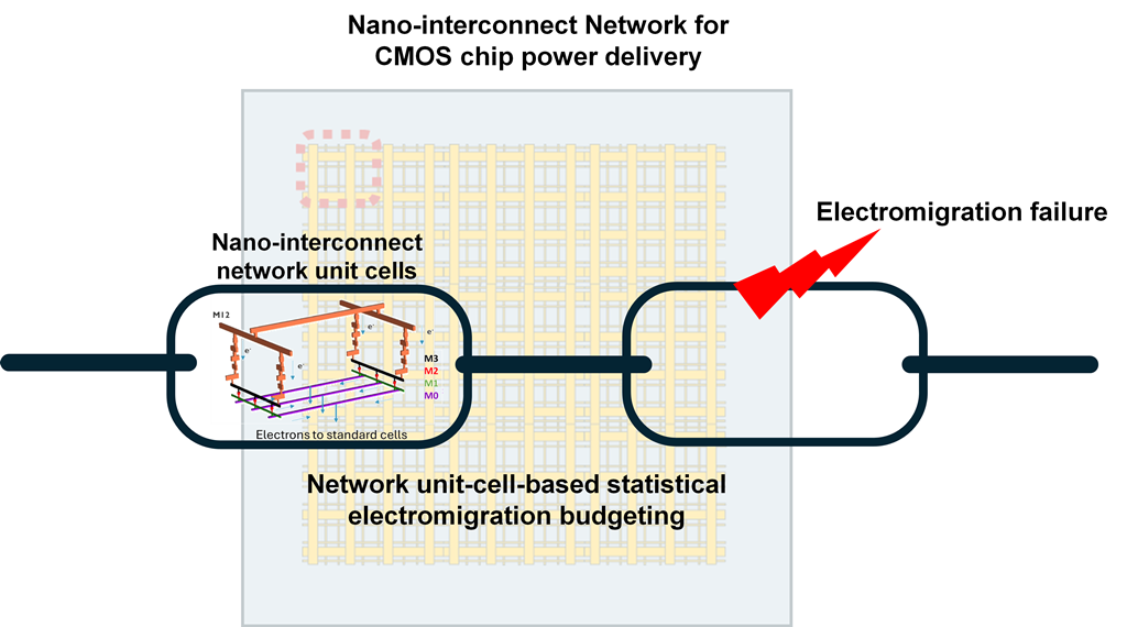
Figure 1.
The PDN-tile-based EM compliance evaluation approach proposed in [66] as compared to the standard approach.
Figure 1.
The PDN-tile-based EM compliance evaluation approach proposed in [66] as compared to the standard approach.
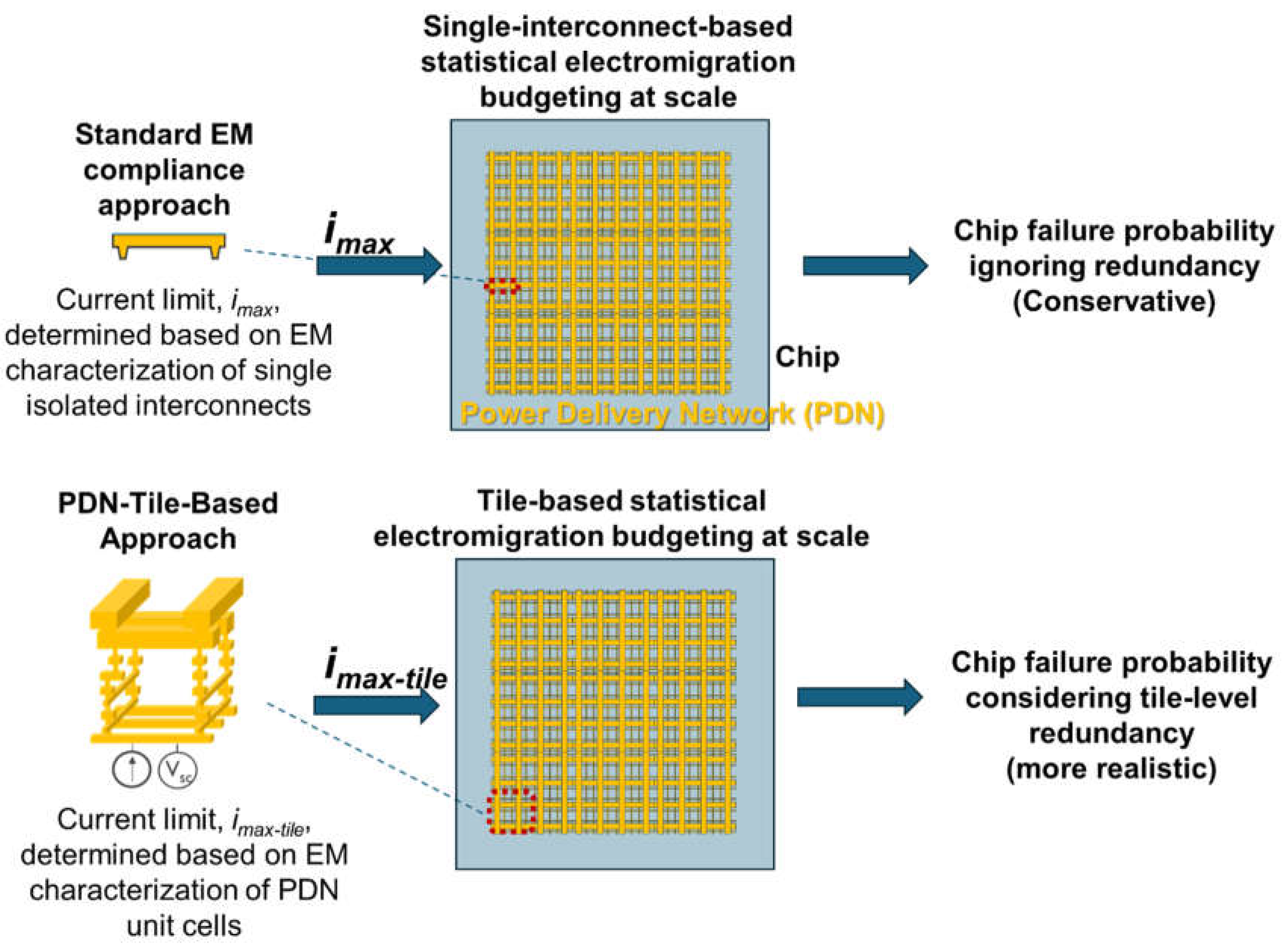
Figure 2.
The diagram of the electrical-EM coupling approach in the simulation framework.
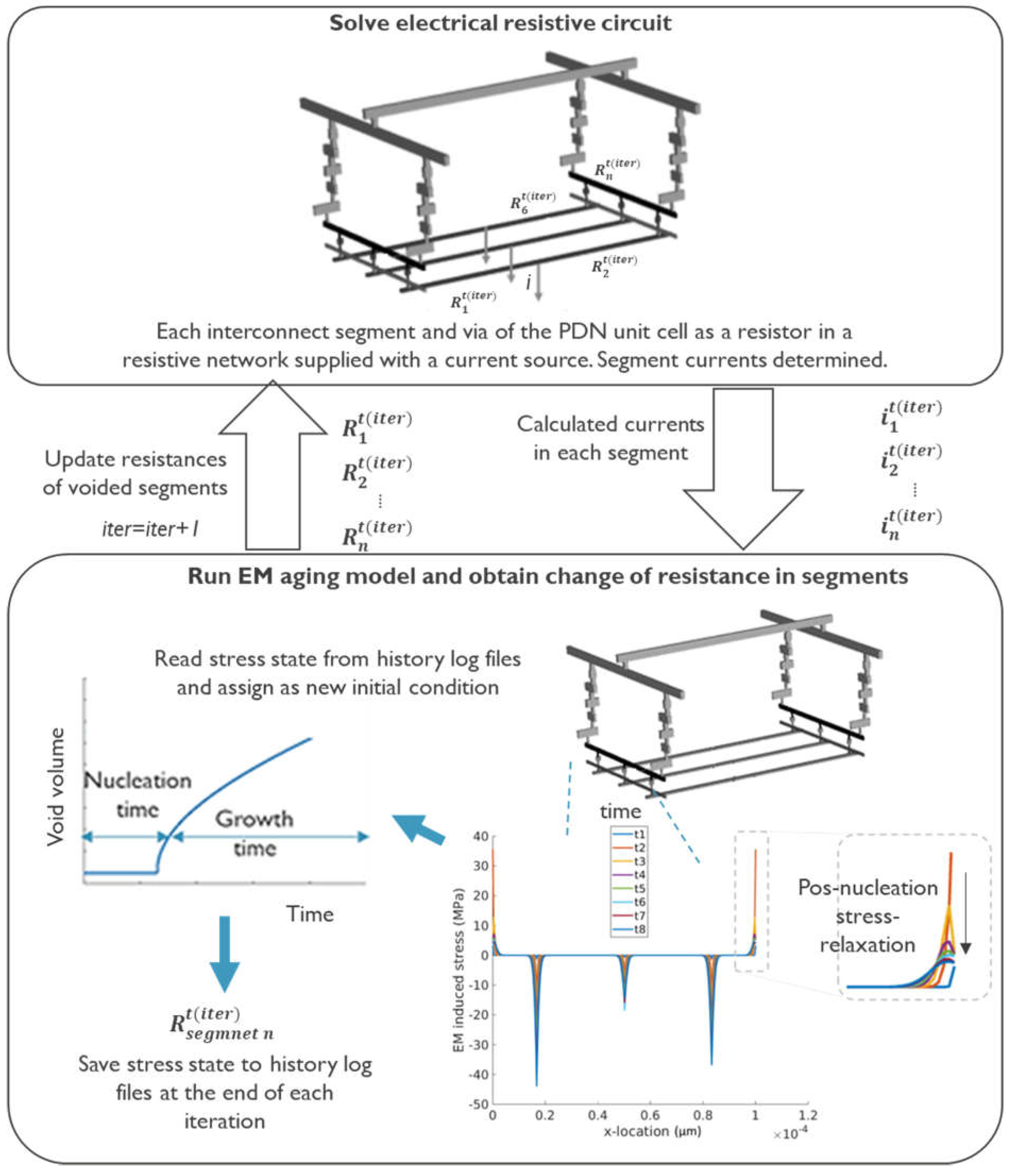
Figure 3.
Distribution of critical electromigration induced stress, .
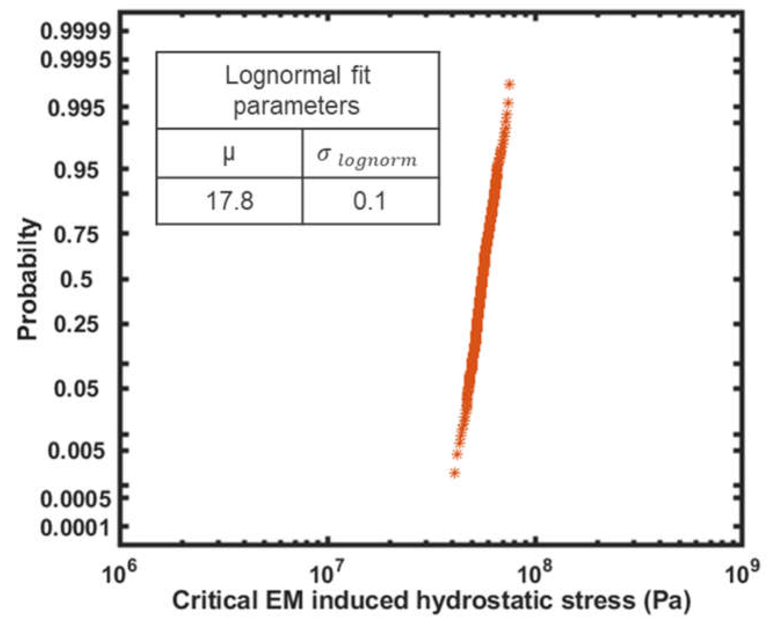
Figure 4.
Calibration of Tgr for a given TTF distribution obtained from single interconnect. (a) TTF (blue) and Tnuc (green) distributions (b) obtained Tgr distribution.
Figure 4.
Calibration of Tgr for a given TTF distribution obtained from single interconnect. (a) TTF (blue) and Tnuc (green) distributions (b) obtained Tgr distribution.
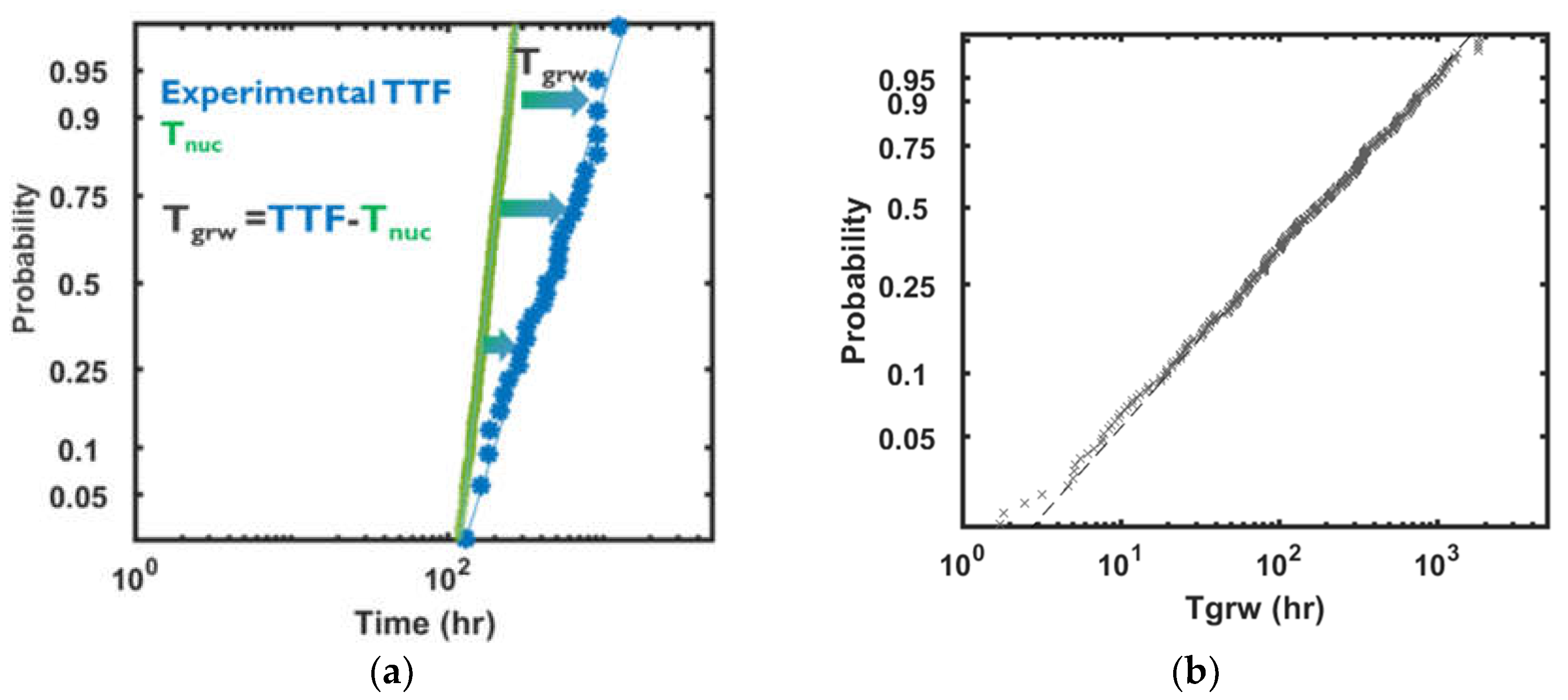
Figure 5.
(a) TTF distributions based on upstream (US) and downstream (DS) EM tests on single interconnects and (b) the deciphered distribution for the two cases.
Figure 5.
(a) TTF distributions based on upstream (US) and downstream (DS) EM tests on single interconnects and (b) the deciphered distribution for the two cases.
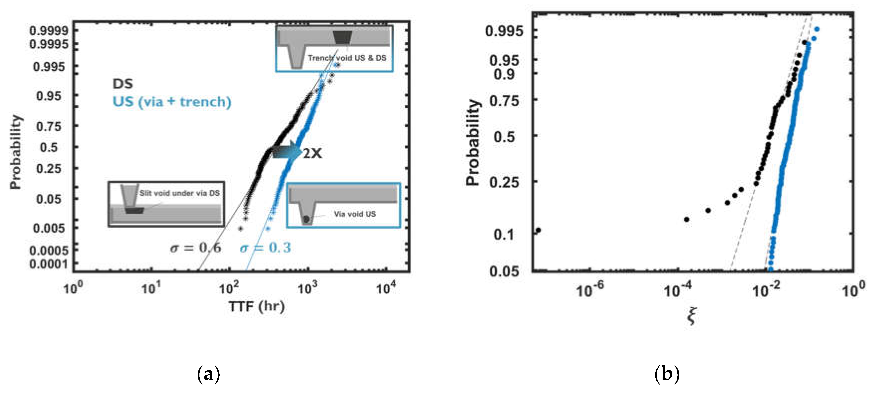
Figure 6.
(a) Considered cases with single interconnect and double interconnects. (b) TTF from Monte-Carlo using experimental distributions (c) Simulated probability plots of TTF distributions using the developed physics-based modelling framework. Continuous line is based on lognormal fit to the data.
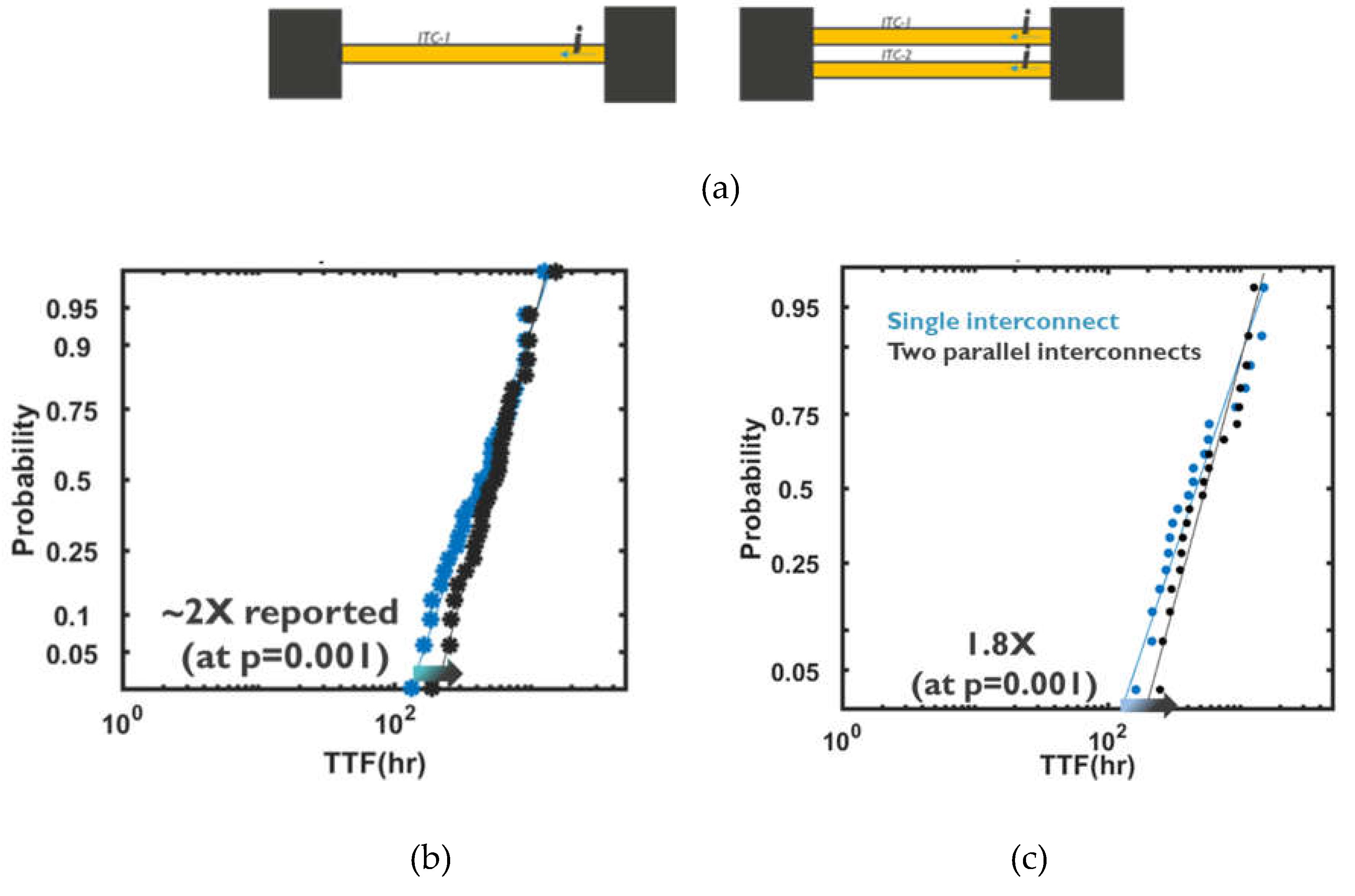
Figure 7.
Schematic of the simulated network with architecture of a PDN tile and its operation under upstream and downstream modes. The blue arrows indicate the direction of electron flow. Vertical and horizontal connections in each BEOL layer are referred to as vias and lines, respectively.
Figure 7.
Schematic of the simulated network with architecture of a PDN tile and its operation under upstream and downstream modes. The blue arrows indicate the direction of electron flow. Vertical and horizontal connections in each BEOL layer are referred to as vias and lines, respectively.
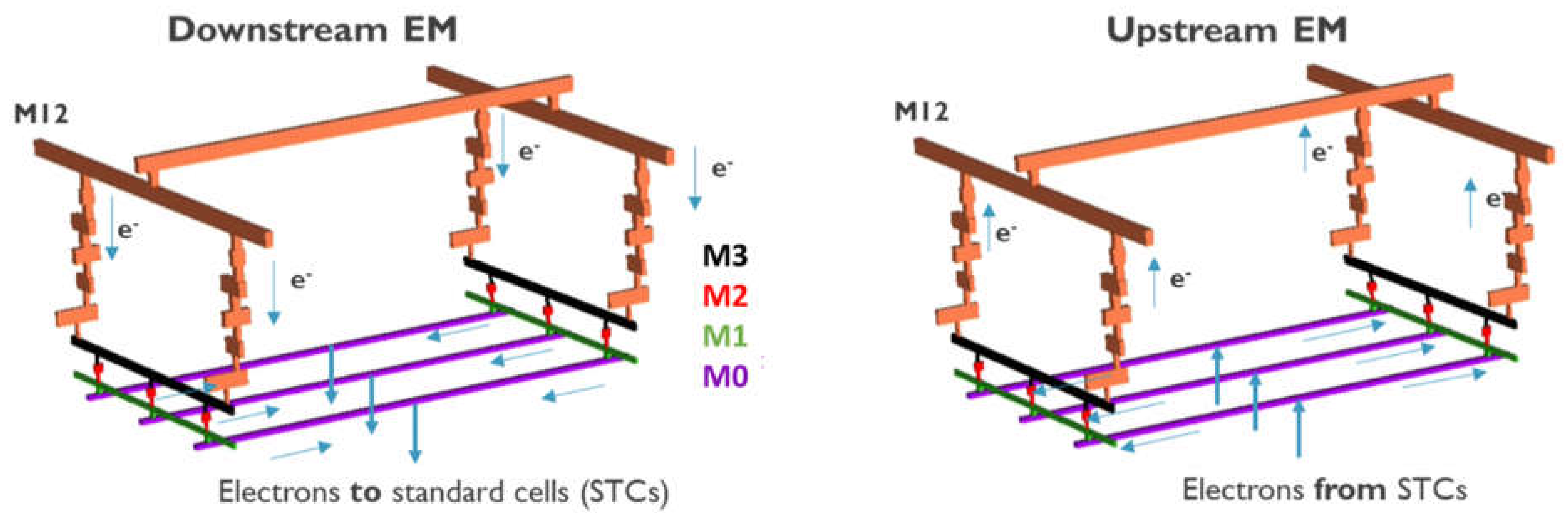
Figure 8.
Transient stress distribution along M3 where void nucleation occurred at the two ends under downstream operation mode. Colours depict different time instances spanning from pre- to post-void-nucleation.
Figure 8.
Transient stress distribution along M3 where void nucleation occurred at the two ends under downstream operation mode. Colours depict different time instances spanning from pre- to post-void-nucleation.
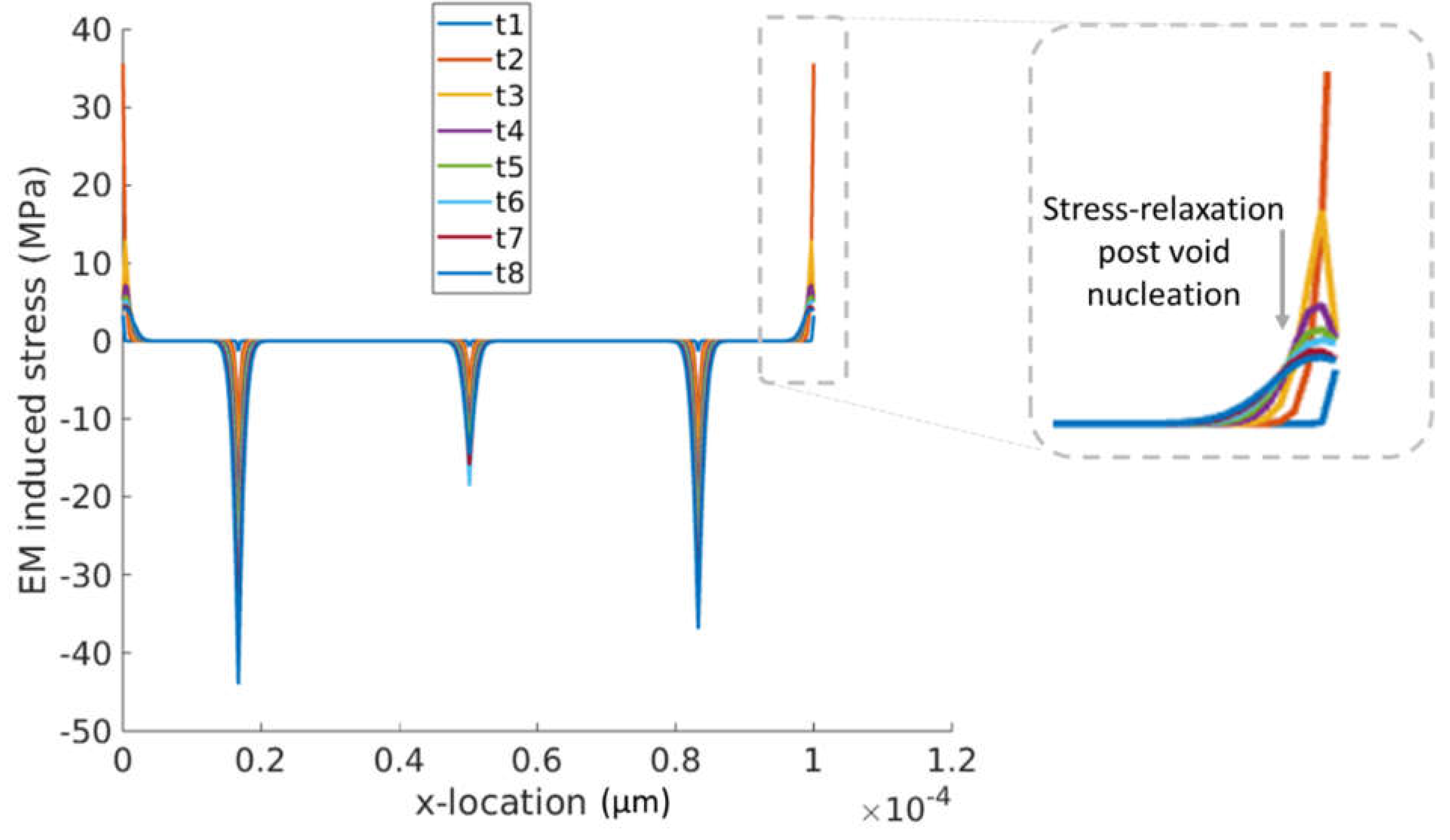
Figure 9.
Stress distribution at steady state along M0, M1 and M3. Stress normalized by the peak stress of each interconnect level. The schematics, show the line-via configurations and the direction of electron flow under upstream and downstream operation.
Figure 9.
Stress distribution at steady state along M0, M1 and M3. Stress normalized by the peak stress of each interconnect level. The schematics, show the line-via configurations and the direction of electron flow under upstream and downstream operation.
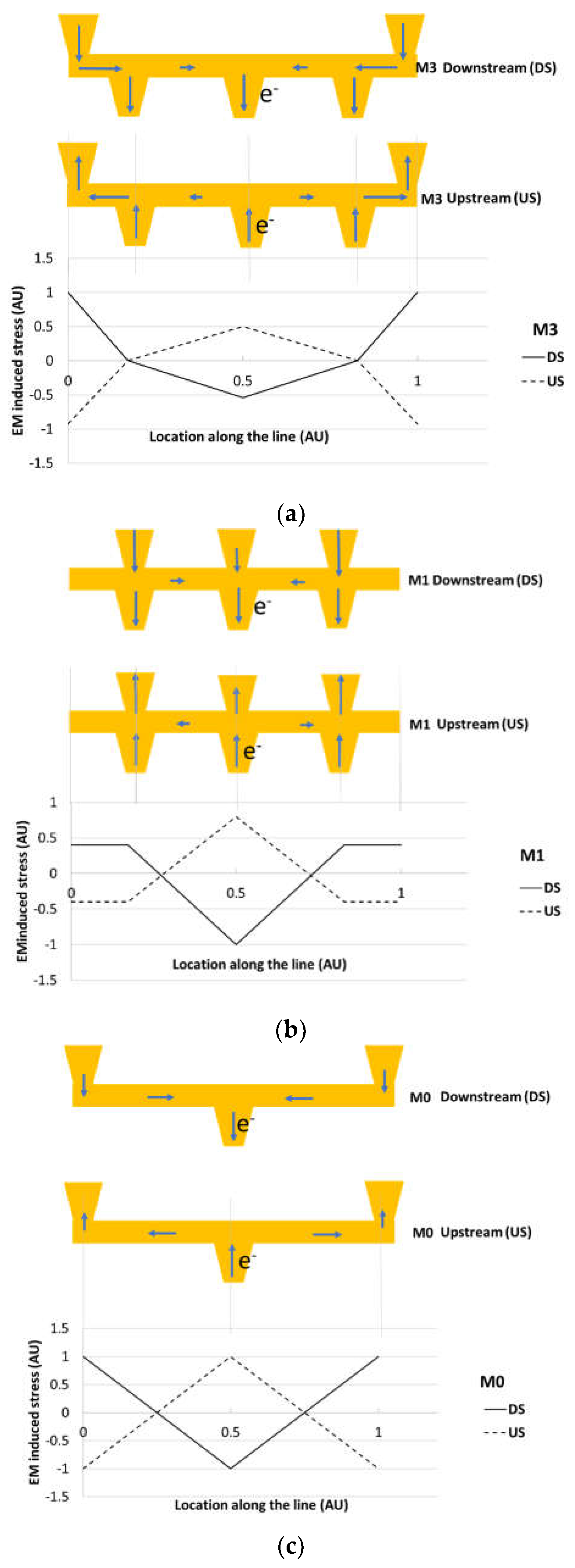
Figure 10.
TTF distribution of the PDN tile shown in Figure 7, supplying same total current under upstream (US) and downstream (DS) operation modes. .
Figure 10.
TTF distribution of the PDN tile shown in Figure 7, supplying same total current under upstream (US) and downstream (DS) operation modes. .
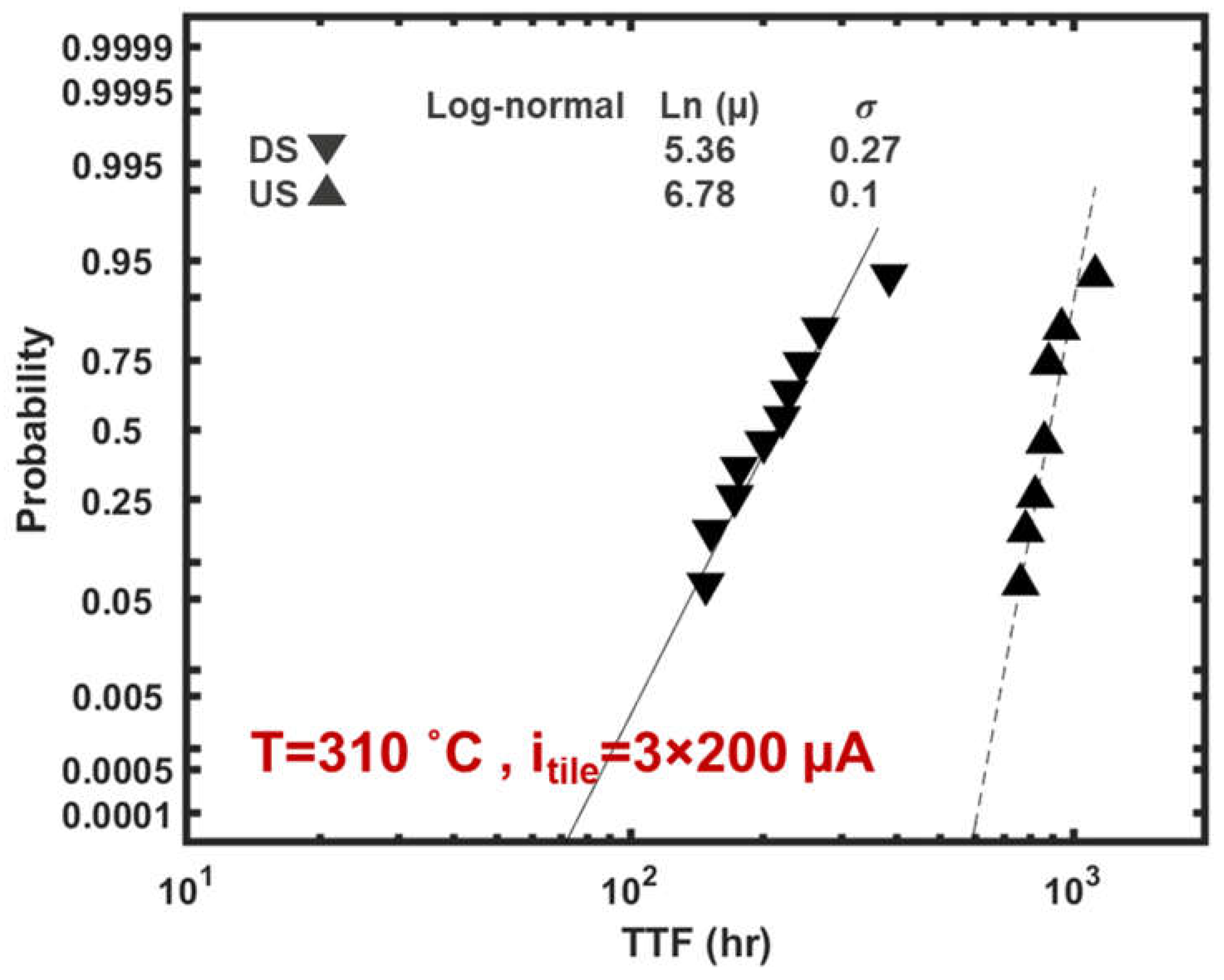
Figure 11.
Cumulative distribution function (CDF) of the TTF of the PDN tile shown in Figure 7, where the impact of redundancy is considered by employing the calibrated modelling framework. The data were fit with a lognormal function. For a target lifetime of 100 hours, the probability of failure is 0.26%.
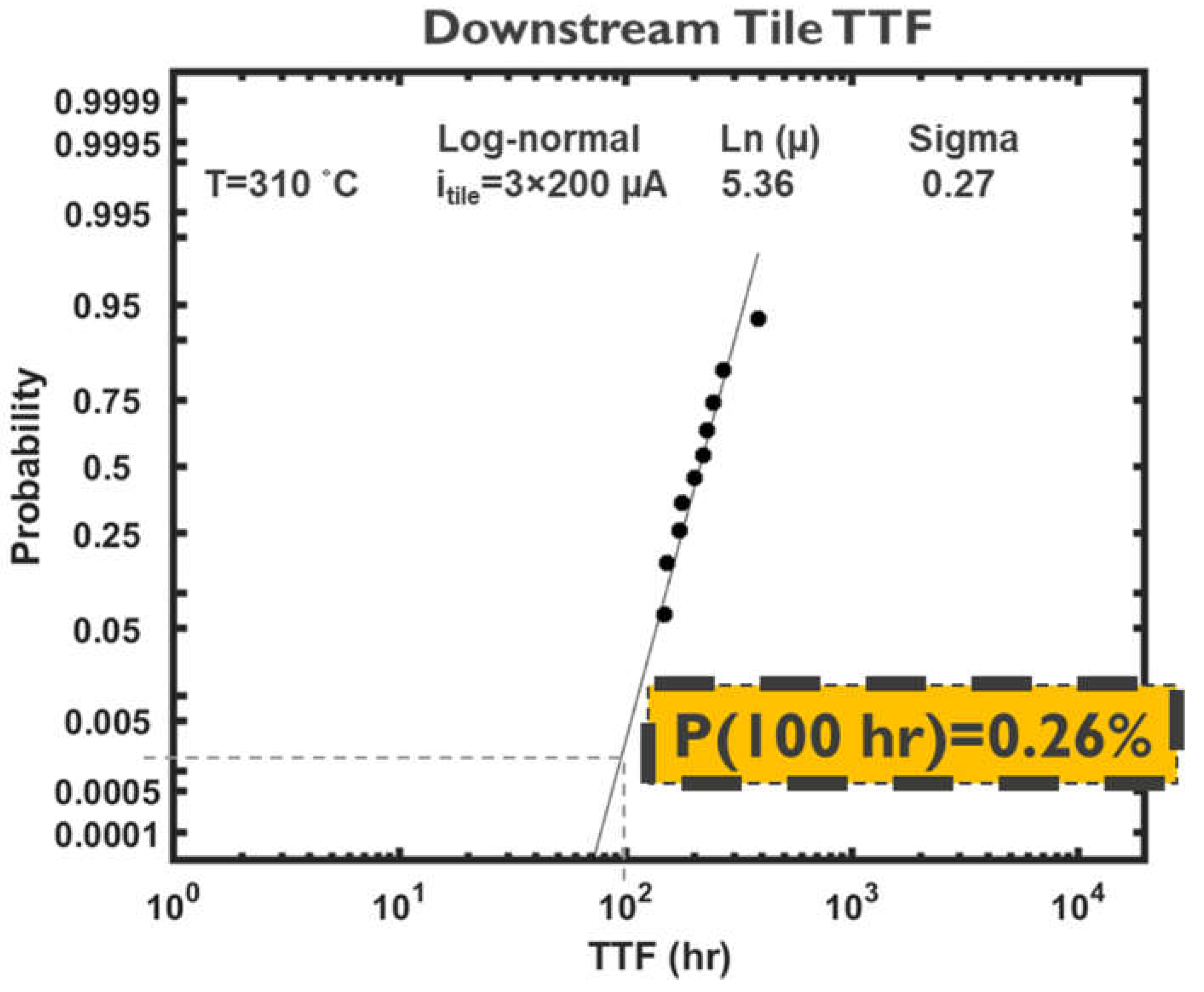
Figure 12.
Impact of current on failure probability prediction by standard SEB (ignoring redundancy) for the PDN tile shown in Figure 7.
Figure 12.
Impact of current on failure probability prediction by standard SEB (ignoring redundancy) for the PDN tile shown in Figure 7.
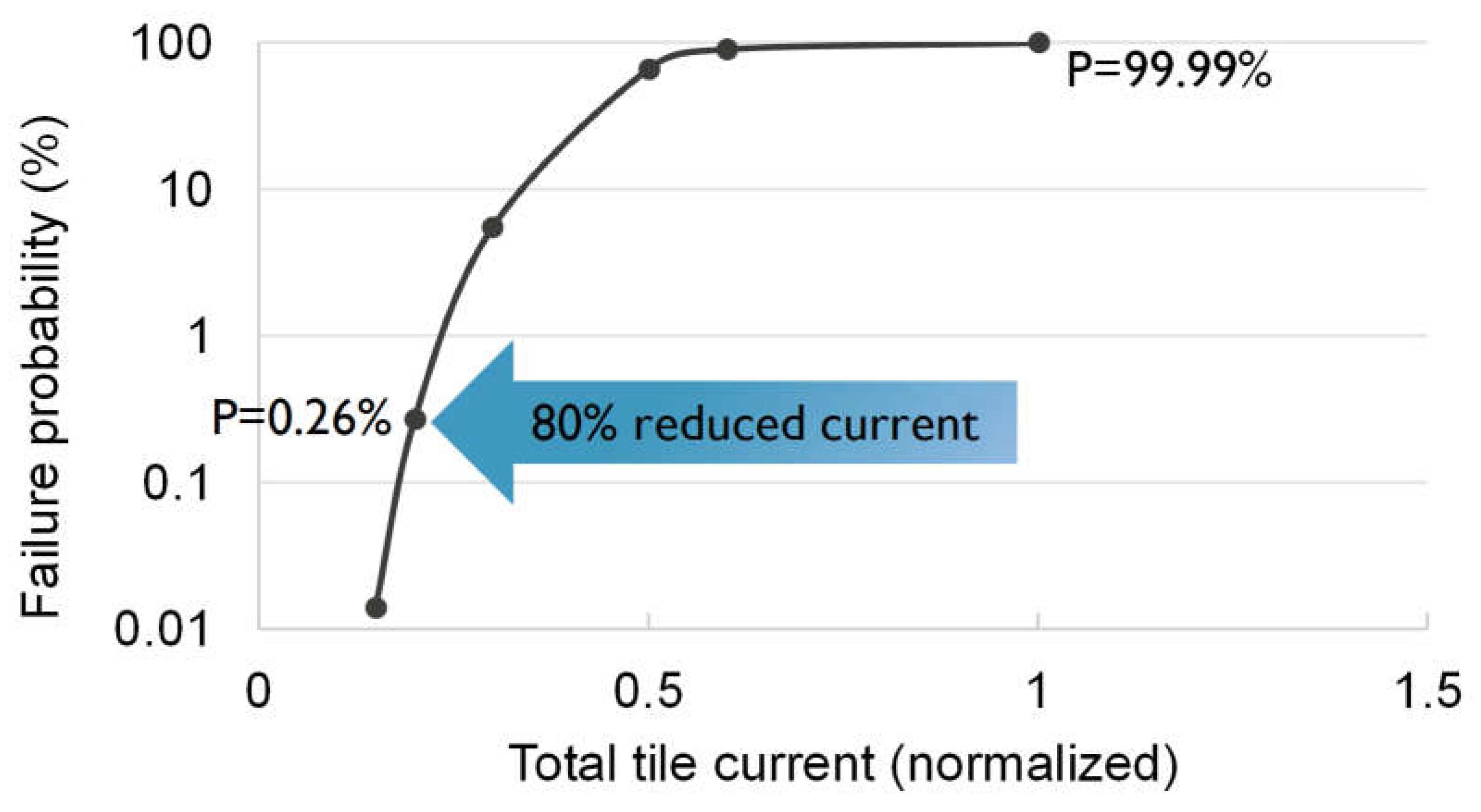
Figure 13.
Impact of failure criterion on PDN tile TTF distributions. Tile failure criterion expressed as the peak EM induced voltage shift in percent at the three current supply points in the middle of M0 lines as shown in Figure 7.
Figure 13.
Impact of failure criterion on PDN tile TTF distributions. Tile failure criterion expressed as the peak EM induced voltage shift in percent at the three current supply points in the middle of M0 lines as shown in Figure 7.
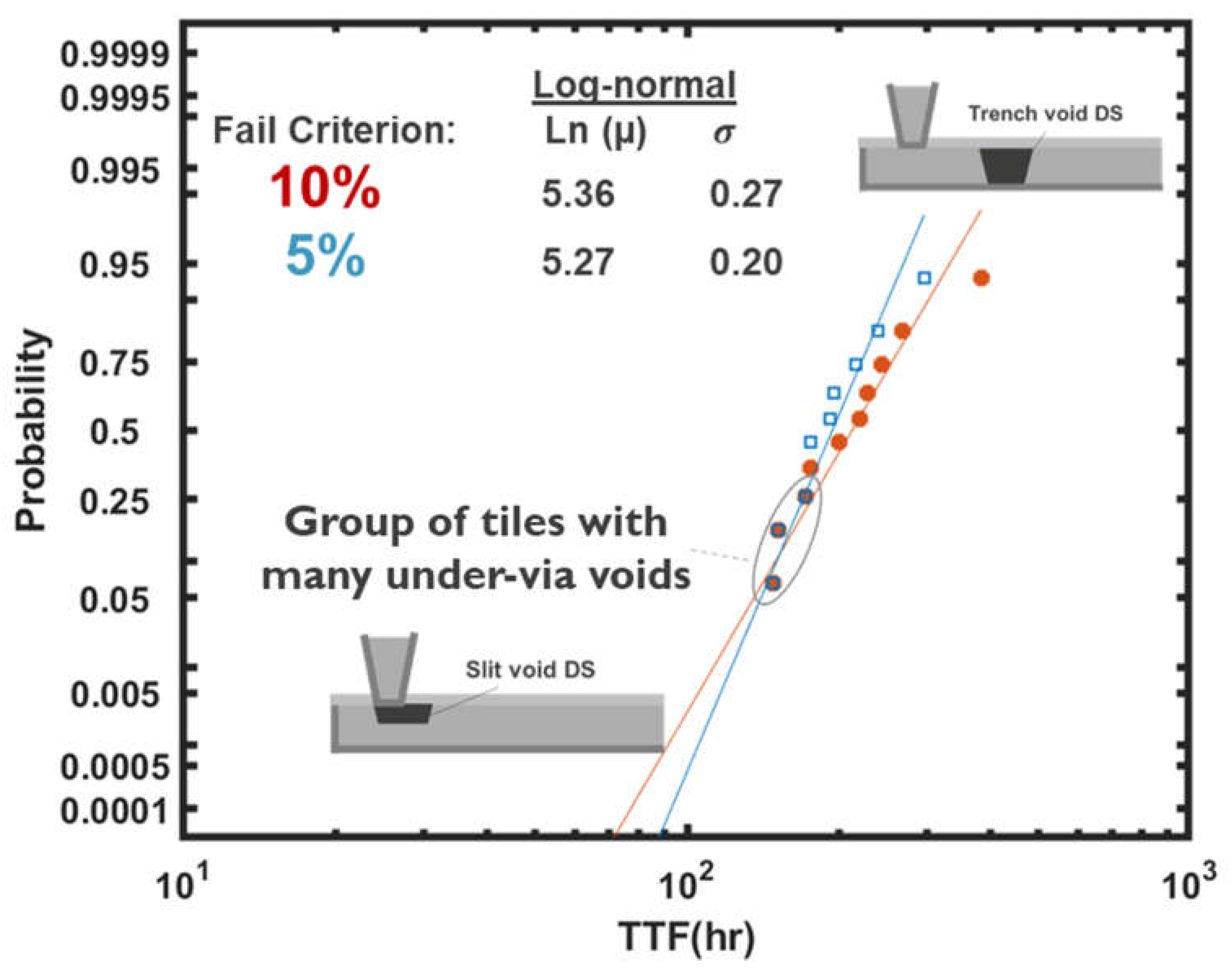

Table 1.
Interconnect geometrical and technological specifications and related physical input parameters for the electromigration model.
Table 1.
Interconnect geometrical and technological specifications and related physical input parameters for the electromigration model.
| Parameter | Value | Description |
|---|---|---|
| Atomic Diffusivity | ||
| 49 Ω.nm | Resistivity | |
| 15 GPa | Interconnect effective bulk modulus | |
| w | 45 nm | Linewidth |
| h | 90 nm | Line height |
| 3 | Effective charge | |
| 1.60218×10⁻¹⁹ C | Electronics charge | |
| 1.182×10⁻²⁹ m3 | Atomic volume |
Table 2.
Break-down of ratios for all the single interconnects within the PDN tile shown in Figure 7 and the number of interconnects with the corresponding ratio shown as frequency. Both line and via values are listed.
Table 2.
Break-down of ratios for all the single interconnects within the PDN tile shown in Figure 7 and the number of interconnects with the corresponding ratio shown as frequency. Both line and via values are listed.
| 0 | 0.58 | 0.63 | 0.94 | 1.2 | 1.89 | 3.05 | 3.63 | 4.58 | |
| Freq. | 4 | 4 | 4 | 4 | 8 | 2 | 12 | 4 | 4 |
Disclaimer/Publisher’s Note: The statements, opinions and data contained in all publications are solely those of the individual author(s) and contributor(s) and not of MDPI and/or the editor(s). MDPI and/or the editor(s) disclaim responsibility for any injury to people or property resulting from any ideas, methods, instructions or products referred to in the content. |
© 2024 by the authors. Licensee MDPI, Basel, Switzerland. This article is an open access article distributed under the terms and conditions of the Creative Commons Attribution (CC BY) license (http://creativecommons.org/licenses/by/4.0/).
Copyright: This open access article is published under a Creative Commons CC BY 4.0 license, which permit the free download, distribution, and reuse, provided that the author and preprint are cited in any reuse.


