Submitted:
16 May 2024
Posted:
16 May 2024
Read the latest preprint version here
Abstract
In this study, we explored terahertz (THz) optical properties of the as-deposited and rapid thermal annealing (RTA) at 400°C, 600°C and 800°C of indium-tin-oxide (ITO) thin-films sputtered on high-resistivity silicon (HR-Si) substrate. We further investigated THz frequency dependence complex refractive indices and conductivity of those as-prepared and annealed ITO thin films. We note the transmittance enhanced from 27 % to 39 % for ITO thin film treated with RTA at 800°C while the real part of conductivity improved from 1019 Ω-1∙cm-1 to 4881 Ω-1∙cm-1 for ITO thin film treated with RTA at 600°C in the frequency range of 0.2 to 1 THz. The mobility, carrier concentration, plasma frequency and relaxation time of those sample were also deduced by fitting the experimental results with the Drude-Smith model. For example, the mobility of 29 cm2/V∙s, 110 cm2/V∙s, 226 cm2/V∙s and 70 cm2/V∙s, respectively is deduced for as-deposited, RTA at 400°C, RTA at 600°C and 800°C of ITO thin-films. In addition, the optical bandgap of those ITO thin films were evaluated with a typical Tauc plot showing extrapolation of photon energy spectrum. The transmittance, absorption coefficient and complex refractive indices of those ITO thin films were extracted by Swanepoel method using experimental transmittance and reflectance spectrum throughout the wavelength range from 400 to 1000 nm. Moreover, as expected, the transmittance of the ITO thin film treated with RTA at 800°C is improved at the wavelength of the visible light spectrum. We also displayed the surface morphology, microscopic structural properties and typical chemical composition of as-deposited and RTA at 400°C, RTA at 600°C and 800°C of ITO thin-films. We strongly believed the present study will lead to further enhancement for THz optoelectronics applications.
Keywords:
Terahertz (THz)
; Rapid thermal annealing (RTA)
; Indium tin oxide (ITO)
; Refractive indices
; Conductivity
; Optoelectronics (OE)
1. Introduction
Indium tin oxide (ITO), typically composed of indium oxide (In2O3) with manuable valence states and oxygen vacancy defects in tin oxide (SnO2) [1,2,3,4], has found wide utility as both a highly transparent in the visible light spectrum as well as conductive layer for biasing for electro optical (EO) device applications [5,6,7]. Its versatility satisfies not only the demands of the electronics industry but also those of the photovoltaic and the optoelectronic applications [8,9,10].
Consequently, ITO thin film deposited on various substrates under diverse growth and post-processing conditions have garnered significant attention within the scientific community [11,12,13,14,15]. Recent efforts have focused on enhancing the characteristics of ITO thin film in terms of crystallinity and optical constants, thus expanding their applications considerably. For instance, Shubitidze et al. [16] reported enhanced optical nonlinearity in ITO thin films with anisotropic crystallographic texturing, which further boosted the nonlinear refractive index modulation in ITO thin film when coupled to a silicon dioxide/silicon nitride (SiO2/SiN) multilayer structures. Similarly, Kim et al. [17] employed post-microwave treatment to improve the optical and electrical properties of ITO thin film for solar cell applications.
Rapid thermal annealing (RTA) processes have been widely used to improve optical and electrical properties of as-deposited ITO thin films as a transparent conductive electrode (TCEs) in thin film transistors (TFTs), liquid crystal display (LCD) and other semiconductor devices [18,19,20]. In comparison, furnace annealing [21] took hours while laser annealing [22] is best used for local modification of materials. RTA treatment has been observed to affect the structural properties and energy bandgap of ITO thin films, opening avenues for various potential devices. For instance, Kim et al., [23] reported a high quality RTA-treated ITO films with a low resistivity (ρ) of 3.3 × 10⁻⁴ Ω∙cm and transmittance as high as 90% throughout the total visible range from 400 to 800 nm. This RTA-treated ITO films is also shown an improvement in crystallinity with the increase of RTA temperature at 400°C and above. In another work [24], a highly conductive RTA- proceeds ITO thin films (ρ = 7.4 × 10⁻⁵ Ω∙cm) were obtained. Besides, X-ray diffraction investigations revealed a cubic nanocrystalline structure could possible for the sputter as-deposited ITO thin films. Furthermore, the ITO thin film annealed at moderately high temperature of 600°C by RTA is also applied to improve electrical and optical properties [25].
The ITO thin film in a multilayer structure with RTA process is also holds a great deal of interest. For example, RTA-processed IGZO/ITO multilayer TFTs, when compared to solely RTA-processed IGZO channels, exhibited a negative shift in threshold voltage, along with enhancements in on-to-off current ratio, subthreshold swing, and mobility. These improvements were facilitated by the elimination of donor-like defect states achieved through curing during the RTA process on the ITO electrode layer [26]. In another study proposed by Maniyara et al. [27], an enhancement in the insertion optical loss of the liquid crystal (LC) cell fabricated with RTA-treated ITO-based near-infrared transparent conductors was demonstrated. Interestingly, RTA-treated heterojunctions composed of ITO/Silicon offered high photo-response by forming a rectifying junction at the interface of ITO and Silicon [28].
Recently, the ITO thin films have not only served as TCE materials in the visible light spectral ranges but also gained widespread acceptance in other frequency band including millimeter-wave (mm-wave), infrared (IR) and terahertz (THz) frequency spectrums [29,30]. For example, Bai et al. [31] proposed a microwave metamaterial absorber composed of conductive ITO thin films and transparent polymethyl methacrylate (PMMA) substrate layers. Additionally, Zheng et al. [32] reported high-performance EO modulators at the communication wavelength of 1550 nm. Moreover, we have demonstrated the enhancemnt of optically excited THz wave emission from a thick layer of ITO thin film coated on semi-insulating gallium arsenide (SI-GaAs) substrate at THz frequencies [33]. Meanwhile, Lu et al. [34] proposed the full-scope of functionality of the ultrathin ITO thin film as an innovative platform for generating broadband THz waves. Further, RTA treatment of ITO thin films has been shown to be an effective way to produce highly reflective ITO thin film for THz absorber applications [35]. A preliminary study on improvement in THz transmittance of RTA-treated ITO thin films were conducted by the authors, as reported in a conference paper [36].
In this paper, we investigate the THz optical and electrical constants of as-deposited and RTA-treated ITO thin films annealed at temperatures of 400°C, 600°C and 800°C using transmission-type THz time-domain spectroscopy (THz-TDS). We utilize the Drude-Smith model to fit experimental conductivity data and calculate THz electrical parameters such as electron mobility, plasma frequency, relaxation time, and carrier concentration. Furthermore, we explore the improvement in THz transmittance resulting from RTA at 800°C, investigating structural properties such as surface roughness and particle size of the ITO thin film. Our ultimate goal is to identify RTA-treated ITO thin films as prospective TCE materials for THz EO device applications.
Additionally, we analyze the transmittance, absorption coefficient, and complex refractive indices of these ITO thin films in the visible (VIS)-near infrared (NIR) light range. We believe this investigation not only presents potential TCEs for next-generation THz EO devices but also sheds light on visible optical properties of ITO thin films annealed at relatively high temperature, an area with limited existing research.
2. Materials and Methods
We selected high-resistive (HR) silicon substrates with two-side polishing (thickness ~ 350 ± 15 µm) to examine the structural, composition and THz optical and electrical properties of the ITO thin films. Fused silica sheets (thickness ~ 800 ± 25 µm) were employed as substrates to study optical properties of the ITO thin films. in visible light spectrum Prior to deposition, the substrates underwent a rigorous cleaning process involving sequential immersion in acetone, isopropyl alcohol and de-ionized water in an ultrasonic cleaner, followed by baking and cooling.
The deposition of ITO thin films was carried out using a radio frequency magnetron sputtering machine (RF Sputter, ULVAC RFS-200S). A 4-inch diameter ITO target with composition of indium oxide/tin oxide (In2O3/SnO2 = 90/10 wt. %) was employed for this study. The pre-deposition vacuum pressure was 5.2 × 10⁻⁶ torr. During deposition, argon (flow rate ~ 50 SCCM)) were introduced into the chamber and maintained at the vacuum pressure of 5 × 10⁻⁵ Torr. The deposition power of 60 W was kept constant at the time of pre-deposition for 6 minutes and deposition for 20 minutes of ITO thin films. ITO thin film were then grown on both HR silicon and fused silica substrate but without heating substrate holder. Yet, the temperature of chamber varied from 20°C to 45°C due to movement of molecules at the time of deposition of ITO thin film. Finally, the chamber was cooled down to room temperature after finish the deposition of ITO thin film and before vent the chamber.
Subsequently, rapid thermal annealing (Premtex RTP-S61-M) were performed at 400°C, 600°C and 800°C for 90 seconds in a nitrogen ambient (flow rate ~ 33 SCCM). The as-deposited ITO thin films and RTA-treated samples were analyzed by a homemade photoconductive antenna based THz-TDS system [37,38]. Additionally, the structural and morphological properties were investigated by using atomic force microscopy (AFM, SEIKO SPA-300HV) and field emission scanning electron microscope (FESEM, JSM-7000F, Japan Electron Optics Labortary Co., Ltd.). The composition of as-deposited and RTA treated ITO thin films was evaluated using energy-dispersive X-ray spectroscopy (EDS). Furthermore, transmittance and reflection data in the visible light range (250 to 800 nm) of the ITO thin films were obtained using an (UV-VIS) spectrometer (Hitachi U-4100).
3. Results and Discussion
This section is organized as follows. First, Subsection 3.1, the structural, surface morphology and composition of interested samples used this study are display. The THz optical and electrical properties of those samples are display in Subsection 3.2. Finally, we briefly study the optical properties of those samples in visible light spectrum for a comparison in the Subsection 3.3.
3.1. Surface Morphology, Composition and Structral Properties
In Figure 1a, we present the SEM images of the top view of the as-deposited ITO thin film, revealing a smooth surface morphology. Additionally, Figure 1b displays the cross-sectional view of the as-deposited ITO thin film, indicating a thickness of 275±6 nm. Figure 1c illustrates the surface morphology of the ITO thin film treated with RTA at 400°C, showing a distinguishable structural transition from that of the as-deposited film while maintaining a flat surface. The thickness of ITO thin film treated with RTA at 400°C is not investigated (as specified by N/A in Figure 1d). On the other hand, the surface morphology of the ITO thin film treated with slightly higher temperature of 600°C is showing a similar that that of RTA at 400°C. This is shown in Figure 1e. We note further the thickness of the RTA-treated at 600°C ITO thin film is slightly reduced to 273±3 nm, as confirmed by the cross-sectional SEM image in Figure 1f. This reduction in thickness may be attributed to the minimization of defects or an increase in density of surface area to volume ratio [39]. Notably, a remarkable change in surface morphology of the ITO thin film treated with RTA at 800°C is observed, as depicted in Figure 1g, where prominent but non-uniform particles are evident. From image analysis of the SEM pictures (ImageJ, University of Wisconsin-Madison, USA), we estimate that the average grain sizes are 80 nm2, 175 nm2 and 694 nm2 for those annealed at 400°C, 600°C and 800°C, respectively. The results indicate a significant increase in grain sizes of the ITO thin films as the RTA temperature increases from 400 to 800°C, a phenomenon also observed in furnace annealing at 550°C for 1 hour [40]. Moreover, the thickness of the ITO thin film treated with RTA at 800°C is approximately 273±2 nm, similar to that of the film treated at 600°C, as confirmed by the cross-sectional image shown in Figure 1h. While we did not perform X-Ray Diffraction (XRD) measurements, it is plausible that our samples, as-deposited is amorphous and annealed are polycrystalline.
Next, AFM was employed to determine the surface roughness and particle size of the ITO thin films. Figure 2a–d display the surface topography of the as-deposited, RTA-treated at 400°C, RTA-treated at 600°C, and RTA-treated at 800°C ITO thin films, respectively. The root mean square (RMS) roughnesses of the as-deposited ITO thin film is 1.5 nm, whereas RTA-treated at 400°C, 600°C, and 800°C ITO thin films are 3.4, 3.5 nm, and 8.3 nm, respectively. The increasing surface roughness with increasing temperature is suspected to be due to structural changes as the ITO thin films become polycrystalline and the grain sizes increase with heat treatment. This increasing trend is in agreement with RTA treated ITO thin film reported by Song et al [25]. It is worth to noting that the RMS roughness nearly same for RTA treated at 400°C and 600°C ITO thin film, showing again similar trend in agrement with Song et al. [25]. To confirm this hypothesis on grain sizes increase with heat treatment, the particle size of the films was examined using AFM, as shown in Figure 5e–h. The calculated particle sizes of the as-deposited, RTA-treated at 400°C, RTA-treated at 600°C, and RTA-treated at 800°C ITO thin films are 37 nm, 62 nm, 85 nm, and 243 nm, respectively. These are in good agreement with the high-resolution SEM study (see Figure 1). The trend of particle size increasing as the increased of annealing temperature was also found in previous literature [41].
Energy-dispersive X-ray spectroscopy (EDS) was utilized for the elemental analysis of the samples of interest. Figure 3a–c show the EDS spectra confirming the presence of all related elements, i.e., indium (In), tin (Sn), and oxygen (O). Furthermore, the weight and atomic percentages of all elements recorded by EDS for these samples are displayed in Table 1. The EDS spectrscopy studiy on RTA-treated at 400°C ITO thin film is not conducted.
We note a trend of increasing weight and atomic percentage of oxygen (O) from the as-deposited (weight: 22.78%, atomic: 68.01%) to RTA-treated at 600°C (weight: 22.98%, atomic: 68.23%) to RTA-treated at 800°C (weight: 24.71%, atomic: 70.27%) ITO samples. This trend is suspected to be due to the increasing oxygen partial pressure in the environment. Similar phenomena were reported in spinel-type nickel manganite oxide (NiMn2O4-δ) polycrystalline samples treated at high temperatures of 800°C [42]. Conversely, indium (In L) recorded higher values in both weight (69.48%) and atomic (28.75%) percentages in RTA-treated 600°C ITO samples compared to the as-deposited ones (weight: 67.44%, atomic: 28.05%). In contrast, tin (Sn L) exhibited lower values in both weight (7.54%) and atomic (3.02%) percentages in RTA-treated 600°C ITO samples compared to the as-deposited ITO thin film (weight: 9.77%, atomic: 3.93%). In a related study by Thirumoorthi et al. [43], and Seki et al. [44], revealed that the resistivity is decreased, carrier concentration is increased and mobility is increased as increasing Sn L concentrations due to the valence difference between Sn L and In L ion ions. Thus, we expect an improvement in THz electrical properties with RTA-treated at 600°C compared to the as-deposited and RTA-treated at 800°C ITO thin film.
3.2. THz Optical and Electrical Properties
The THz frequency-dependent optical properties of as-deposited and RTA-treated ITO thin films coated on HR silicon and the reference (bare HR silicon) were studied by using a home-made transmission-type THz-TDS system. The THz pulse train transmitted through the reference and ITO/HR silicon are shown in Figure 4a. A small-time delay due to discernible phase shift of the THz pulse transmitted through the samples under study can readily be seen. Next, a Fast Fourier Transform (FFT) algorithm was applied to convert the THz time-domain signal to its spectral amplitudes. These are displayed in Figure 4b. The data, i.e., time-delay or phase shift and attenuation imply significant interaction between the THz wave and materials investigated. The inset of Figure 4b shows an example of a nearly perfect phase linearity of transmitted THz field through all the samples in the frequency range from 0.2 to 1.2 THz. This is a testimony of the reliability of the THz-TDS spectrometer.
For extraction of the optical constants, we employ the same approach as in our previous works on various thin films and nanostructures [33,45,46,47,48,49,50]. We reiterate here for the benefits of readers: Consider the ITO layer (subscripted as 2) to be sandwiched between air (subscripted as 1) and a substrate (subscripted as 3) with complex refractive indices n2, n1 and n3, respectively. The THz wave is assumed to be incident on this thin layer with a thickness of d from the air toward the substrate. Considering multiple reflections [51], the transmitted THz electric field through the ITO-coated substrate can be written as
where E0, t12, t23, t31, r21, and r23 are the incident electric field, transmission, reflection coefficients between various interfaces; ω is the angular frequency; c is the speed of the light in vacuum; D is the thickness of substrate. Similarly, a reference THz field defined as the THz field transmitted through the bare substrate can be written as
The transfer function of the THz wave through the ITO layer then can be written as
Experimentally, texp(ω, n2) is obtained from ratios of the frequency components of the Fourier transforms of the measured THz waveforms through the as-deposited and annealed ITO/HR-Si and the bare substrate. An error function Error(ω, n2) is defined as follows:
By minimizing the error function, the real and imaginary parts of the complex refractive index n2 of the thin film layer can be deduced.
Figure 5 shows the real (n) and imaginary (κ) part of refractive indices of as-deposited and RTA-treated ITO films at 400°C, 600° and 800°C as a function of frequency. In the frequency range of 0.2-1.0 THz, as-deposited ITO thin film exhibits a decreasing trend in n from ~ 65 to ~ 33, and κ from ~ 66 to ~ 27. Such decreasing trend and values of optical constants for as-deposited ITO thin film are very close to those of the DC-magnetron-sputtered and electron-beam-deposited ITO thin films reported previously by us [45,46,47,48,51] as well as pulsed laser deposited ITO thin film reported by Wang et al. [52]. This implies that the THz optical constants of ITO films deposited by various methods are very similar. The THz optical constants of RTA-treated ITO thin films also exhibit analogous decreasing trend with increasing frequency. Note, however, the n and κ of ITO films RTA-treated at 400°C and 600°C are almost identical, from ~ 143 to ~ 72 and ~ 131 to ~ 67, respectively over 0.2 – 1.0 THz, but much higher in values in comparison to those of the as-deposited ITO thin film. In contrast, the n values of RTA-treated at 800°C ITO thin film revert back to about the same values as those of the as-deposited sample while the extinction coefficients, κ, are somewhat lower, ranging from ~ 45 to ~ 19, as compared to ~ 66 to ~ 27 of the as-deposited ITO film in the same THz frequency band. These trends correlate with the electrical characteristics of the films to be discussed in a latter paragraph of this section.
Figure 5.
(a) The real (n) and (b) imaginary (κ) part of refractive indices of ITO films as a function of frequency. Black open square: as-deposited, red circles: RTA-treated at 400°C, green open triangles: RTA-treated at 600°C and blue open triangles: RTA-treated at 800°C.
Figure 5.
(a) The real (n) and (b) imaginary (κ) part of refractive indices of ITO films as a function of frequency. Black open square: as-deposited, red circles: RTA-treated at 400°C, green open triangles: RTA-treated at 600°C and blue open triangles: RTA-treated at 800°C.
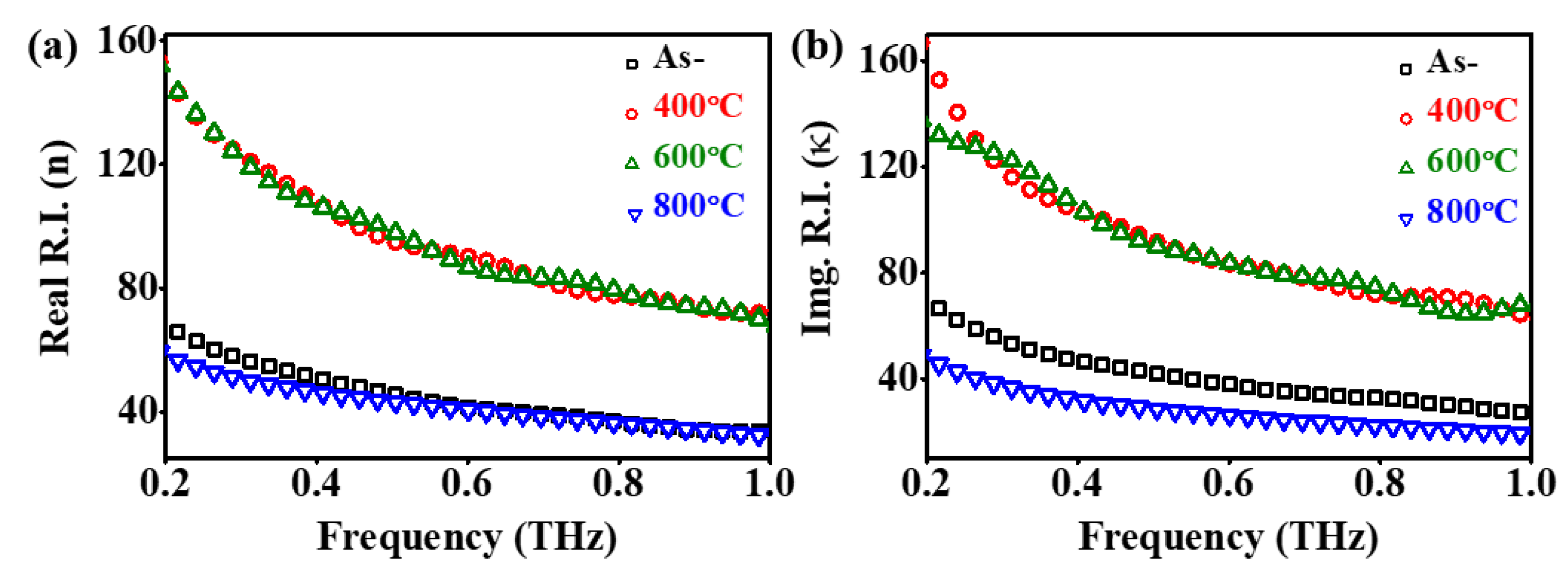
We are not able to verify the THz refractive indices of those RTA-treated ITO thin films due to lack of published literature at the present time. Yet, the increasing of THz refractive index with RTA-treated at 400°C and 600°C is supported with the experimental measurements as well as the numerical estimate in reflectance of DC-magnetron sputtered ITO thin films deposited on glass substrate and post-annealed in the tubular furnace up to 300°C [35]. From our SEM and AFM results, we assumed the increase of refractive indices for RTA-treated ITO films at 400°C and 600°C compared to those of as-deposited samples might be attributed to the increasing of grain size and an improvement in crystalline structure. The behavior of ITO films RTA-treated at 800°C is unique. Structural and morphology studies indicate that the grain sizes and surface roughness for these samples are much larger than those heat-treated at lower temperatures. This could be correlated with the observed trend in this work. We note that almost all of reported studies on the effects of annealing on ITO films were conducted at temperatures below 600°C [53]. Further, these works focus on the optical properties of ITO films, in the visible region (400-700nm). Therefore, we also studied “optical “properties of these ITO thin film in the visible window and present them in the next sub-section.
We next extracted the transmittance of those samples using the ratio of frequency domain THz field amplitudes through the ITO/HR silicon to the frequency domain THz field through the reference (bare HR silicon), see Figure 6a. The THz transmittance of as-deposited and RTA-treated ITO thin films are slow-varying in the band of 0.2 – 1.0 THz. The average transmittance of as-deposited, RTA-treated at 400°C, RTA-treated at 600°C and RTA-treated at 800°C are 27 %, 8%, 8 % and 39 %, respectively. We note the average THz transmittance of as-deposited ITO thin film is somewhat lower than those thinner (~ 100 nm) as-deposited ITO thin films (T ~ 40%) used in our earlier works [54]. This is primarily attributed to the thickness dependent free carrier absorption of ITO thin film. The THz transmittance of ITO thin film treated with RTA at 400°C and 600°C are as low 8 %. This is consistent with higher extinction coefficients of RTA-annealed ITO films at either 400°C or 600°C shown in Figure 5b. Our results indicate that annealing temperature is a critical parameter affecting transmittance and reflectance of the ITO film.
In Figure 6b and c, it can be seen that the absorbance and reflectance of ITO thin films depend strongly on the annealing temperature. Here, absorbance, A, is calculated by A=αd/2.303, where the absorption coefficient α is related to the extinction coefficient κ by 𝛼=4𝜋𝜅/𝜆𝐴. In turn, reflectance of the samples is determined by R =1-T-A. We note that the decreasing trend of reflectance for increasing temperature is consistent with the square root dependence of conductivity according to the Hagen-Rubens approximation [55],, by using the conductivities σ listed in Table 2 of this work. Both absorbance and reflectance are found to be much higher for ITO films heat treated by RTA at 400°C and 600°C than that of as-deposited ones. We speculate that RTA-treated ITO thin films at either 400°C or 600°C could potentially be useful as dichroic mirrors or absorbers for the THz band [35,56]. On the other hand, ITO thin films RTA-treated beyond 800°C could be an effective THz TCE material for THz EO devices. We note the transmittance of ITO-coated device can be further enhanced by employing a grating-like, i.e., wire-grid structure, as we have demonstrated earlier [54].
Electrical characteristics of the ITO films can be extracted from the optical constants determined above. The complex conductivity, σ* is related to the dielectric function,
Where ε0 is the free-space permittivity, ε∞ ~ 4 is the high-frequency dielectric constant of ITO, consisting of contributions from bound electron. Therefore, we can determine THz conductivities of ITO samples from their complex refractive index, i.e.,
In degenerate semiconductors such as ITO, the Drude free-electron model has been most widely used to describe its electrical characteristics. That is,[57], where ωp and τ are plasma frequency and scattering time of carriers in the material. The real part of conductivity, Re{σ}, exhibits a maximum at zero (DC) frequency, and its value decreases with increasing frequency. For Im{σ} [46,47,48], it can only be positive and approaches a maximum as the frequency approaches that of the inverse of the scattering rate. We have found, however, that the THz conductivities of ITO films and nanostructures exhibit non-Drude-like behavior, e.g., depressed values of DC conductivity and negative values for Im{σ} [46,47,48]. Therefore, the Drude-Smith model, which takes into account the carrier localization effect, is chosen to fit the experimentally deduced conductivity of the ITO material, In this model [58],
where c is the persistence of velocity and that varies from -1 to 0. The value of c ( -1 < c < 0) can be associated with the degree of backscattering that a carrier suffers after a collision. When parameter c = 0, the Drude model is recovered. Carriers undergo complete backscattering or localization for c = -1. Although it is a rough approximation, this simple empirical model works remarkably well for a variety of materials. The SEM data show that our ITO samples consists of grains tens to hundreds nanometer in dimension. Thus the non-Drude-like behavior can be contributed by backscattering of carriers at grain boundaries [59,60]. On the other hand, the dopants in ITO will become positive ions after providing free electrons [61,62]. Due to the Coulomb interaction between dopant ions and free electrons, the former will also become scattering centers hindering movement of the electrons as well. As we shall see in Figure 7, the Drude-Smith model fits the conductivity data better than the simple Drude model. All of the fitting parameters are summarized in Table 2. Meanwhile, the extracted motilities (µ) are 29 cm2/V∙s, 110 cm2/V∙s, 226 cm2/V∙s and 70 cm2/V∙s; plasma frequency (ωp) are 3315 rad.THz, 3711 rad.THz, 2580 rad.THz and 1648 rad.THz; scattering times (τ) are 6 fs, 12 fs, 21 fs and 20 fs; the fitting parameters (c) are -0.83, -0.68, -0.63 and -0.87; carrier concentration (N) are 2.17×1020 cm-3, 2.72×1020 cm-3, 1.31×1020 cm-3 and 5.58×1019 cm-3; conductivities (σ) are 1019 Ω-1‧cm-1, 4897 Ω-1‧cm-1, 4881 Ω-1‧cm-1and 628 Ω-1‧cm-1; and resistivity (ρ) are 9.8×10⁻⁴ Ω·cm, 2.0×10⁻⁴ Ω·cm, 2.0×10⁻⁴ Ω·cm and 15.9×10⁻⁴ Ω·cm for as-deposited, RTA-treated at 400°C, RTA-treated at 600°C and RTA-treated at 800°C, respectively.
3.3. Annealing Effects on UV-VIS-NIR Optical Properties of ITO Films
It is interesting to compare the optical properties of samples studied in this work in the ultraviolet (UV), visible (VIS) and near infrared (NIR) band as a bearing on their far infrared (FIR) or THz frequency range. We have experimentally measured transmittance and reflectance of as-deposited and RTA-treated ITO thin films coated on fused silica as well as that of the substrate itself in the energy range of 0.6 eV – 6 eV, or the wavelength band of 200 – 2000 nm. These are shown in Figure 8. The average transmittance in the VIS-NIR region (400-800nm) band for as-deposited ITO film was Tav ~ 72%. After annealing at 400°C, 600°C, and 800°C, Tav ~ 68 %, ~ 80 % and 83%, respectively. Considering the contribution by the substrate, In, all samples can be considered highly transparent in this band. Higher transmittance of samples after heat treatment by annealing can be attributed to increasing sizes of crystallites after annealing as shown in the SEM data (see Figure 1). It is well-known that improved crystallinity leads to reduced scattering of incident light, which enhanced their transmission through the film. Transmittance drops off sharply in the NIR and UV band for all samples. The absorption edge shifted to shorter wavelength for samples annealed at increasingly higher temperatures. This point will be addressed further later on.
The average reflectance of as-deposited ITO thin film in the UV-VIS-NIR region, Rav ~ 14 %. Whereas, the reflectance of ITO thin film with RTA-treated at 400°C, 600°C and 800°C are Rav ~ 10 %, Rav ~12% and Rav ~ 13%, respectively in VIS spectrum wavelengths. In addition, the reflectance curve shows small but yet significant oscillations due to multiple reflections of light within the sample. This also reasonably good agreement with the previous finding by others [ref]. Further, the results show a general increasing trend in reflectance in NIR region with temperature. The trend is quite similar to the literatures reported previous [ref]. It is also observed that the reflectivity increased to 70 % as the annealing temperature was increased to 600°C. This is tentatively attributed to increase of carrier concentration after annealing. Yet, the reflectivity is shown slightly lower for ITO thin film RTA-treated at 800°C than those of other RTA-treated samples. This is probably impacted by surface roughness effects [ref]. Thus, our results indicating annealing can be used to tune the optical transmittance and reflectivity of ITO thin film over a broad band from UV-VIS-NIR to the THz region by changing structural, surface morphology and electrical properties.
We now focus on spectral regions of ITO films that are weakly absorbing and also shown prominent maximum (TM) and minimum (Tm) transmission spectrum, i.e., the visible window of 400-800 nm (see Figure 8a). Following Swanepoel [63], the refractive index of ITO the film in its weakly absorbing VIS-NIR (400 to 1000 nm) band can be estimated as , where , TM and Tm are envelopes of maxima and minima of the transmission curve and is the refractive index of fused silica substrate and is determined using its transmission spectrum (T) to be ~ 1.43, and found to be fairly independent of wavelength. The calculated refractive index n of as-deposited and those RTA-treated ITO thin film in wavelength range from 400 to 1000 nm are shown in Figure 9a. Note that the refractive index of 1.74 in this band is almost wavelength-independent and approximately the same for all types of ITO thin film studied in this work. Note a small dispersion-like feature of the refractive index was observed near 500 nm. It can be seen that the refractive indices of annealed ITO films are lower than those of the as-deposited one in this dispersion region. In the literature, the reported refractive indices for as deposited as well as annealed ITO thin films vary from 1.6 to 2 in this band [64].
The thickness d of those ITO thin films can be determined using the envelopes of maxima and minima of the transmission curve in the visible spectra, , where n1 and n2 are the refractive indices at two adjacent maxima or minima, TM or Tm , corresponding to wavelengths at λ1 and λ2, respectively. The estimated thickness of as-deposited and RTA-treated ITO thin films at 400°C, 600°C and 800°C are ~ 470 nm, ~ 410 nm, ~ 483 nm and ~ 468 nm, respectively. Knowing the thickness of ITO thin films, the absorption coefficient α of these samples are extracted using the relationship between transmittance (T), reflectance (R) in VIS spectrum range and thickness d, given: . Next, the imaginary part of refractive index κ as the function of wavelength is evaluated using another simple formula shown as:, plotted in Figure 9b. We found that κ in the wavelength range of 400 to 1000 nm is slow varying and approximately 0.04, 0.18, 0.13 and 0.7 for as-deposited and RTA-treated ITO thin films at 400°C, 600°C and 800°C, respectively. Such estimated values are also in agreement with those reported in previous works [64].
Crystalline ITO has been shown to be a direct gap semiconductor [65]. From the absorption coefficient α as plotted in Figure 10a, the optical bandgap Eg can be extracted using the extrapolation method proposed by Tauc: (αhʋ)2 = A (hʋ-Eg) [66]; Where A is a constant and h = 6.626×10⁻³⁴ J.s is the Planck constant. These are shown for the samples under study in Figure 9b. The optical band gap Eg of as-deposited ITO thin film was found to be 3.6 eV. On the other, the optical band gap Eg for RTA-treated ITO thin films at 400°C, 600°C and 800°C are estimated to be approximately 3.97 eV, 4.10 eV and 4.11 eV, respectively. The increasing Eg as the annealing temperature increases ascribed primary to the improvement of the crystallinity and reducing the defects in thin film. Nevertheless, these values are good agreement with typical value reported previously. For example, Abd-Elnaiem et al. [67], extracted Eg for as-deposited and for annealed ITO thin film with thickness of 80 nm at 300°C to be ~ 3.2 eV and~ 3.8 eV, respectively. Meanwhile, Eg for a 200 nm-thick ITO films heat-treated with RTA at 600°C was determined to be as high as 4.04 eV by Song et al. [25].
4. Conclusions
Our study presents significant advancements in terahertz (THz) optical properties achieved through rapid thermal annealing (RTA) treatment of indium tin oxide (ITO) thin films deposited on high-resistivity (HR) silicon substrates. We observed improved THz transmittance upon RTA at 800°C, and enhanced THz reflectance following RTA at either 400°C or 600°C. Notably, our investigation reveals a substantial tunability in the complex refractive index, with both the real (n) and imaginary (κ) components exhibiting notable variation across THz frequencies. Employing the Drude and Drude-Smith models, we successfully extracted key electrical parameters such as plasma frequencies, scattering times, mobility, and conductivities of the ITO thin films. Our findings demonstrate a notable increase in free carrier concentration in RTA-treated samples compared to as-deposited ones, resulting in improved mobility and conductivity. This enhancement in THz optical and electrical properties is attributed to intricate changes in surface morphology, crystalline structure, and composition properties induced by RTA treatment. Furthermore, we effectively employed noncontact terahertz time-domain spectroscopy (THz-TDS) to characterize the dielectric and electrical properties of both as-deposited and RTA-treated ITO thin films. Remarkably, high-temperature RTA at 800°C facilitated the formation of large nano-granular ITO particles without any crack formation in the thin films. Optical characterization studies reveal the highest transmittance in the visible spectrum and optimal optical bandgap with ITO thin films annealed at 800°C. Additionally, we derived complex refractive indices across the 400 nm to 1000 nm range using the Swaneepoel's method. Future investigations will delve into the optical and electrical properties of ITO samples in the far-infrared (FIR) region. Overall, our study offers valuable insights into leveraging RTA treatment to enhance THz optical properties, with potential applications spanning from coatings for waveguides to THz electro-optic (EO) switching devices and manipulation of THz electromagnetic waves.
Author Contributions
Conceptualization, C.L.P. and A.K.S.; methodology, C.L.P and A.K.S.; software, W.C.A and A.K.S; validation, C.L.P, A.K.S. and W.C.A.; formal analysis, C.L.P, A.K.S. and W.C.A.; investigation, C.L.P, A.K.S. and W.C.A.; resources, C.L.P.; data curation, A.K.S.; writing—original draft preparation, A.K.S; writing—review and editing, C.L.P; visualization, C.L.P; supervision, C.L.P; project administration, C.L.P; funding acquisition, C.L.P. All authors have read and agreed to the published version of the manuscript.
Funding
This research was funded by the Ministry of Science and Technology renamed to, National Science and Technology Council, Taiwan, under various grants.
Institutional Review Board Statement
Not applicable.
Informed Consent Statement
Not applicable.
Data Availability Statement
The data presented in this study are available on request from the corresponding author.
Acknowledgments
A. K. S. would like to thank Mr. Chia-Ming Mai for THz-TDS measurement. The authors would like to thank Prof. Peichen Yu from National Yang Ming Chiao Tung University Taiwan, for use of the UV-VIS-NIR spectrometer. They would also like to thank the Center for Nanotechnology, Materials Science, and Microsystems (CNMM), NTHU, where the samples were fabricated.
Conflicts of Interest
The authors declare no conflicts of interest.
References
- Tripathi, M.N.; Bahramy, M.S.; Shida, K.; Sahara, R.; Mizuseki, H.; Kawazoe, Y. Optoelectronic and magnetic properties of Mn-doped indium tin oxide: A first-principles study. J. Appl. Phys. 2012, 112, 073105. [Google Scholar] [CrossRef]
- Hamberg, I.; Granqvist, C. G. Evaporated Sn-doped In2O3 films: Basic optical properties and applications to energy-efficient windows, J. Appl. Phys. 60, 1986, R123–R160.
- Li, S.; Tian, M.; Gao, Q.; Wang, M.; Li, T.; Hu, Q.; Li, X.; Wu, Y. Nanometre-thin indium tin oxide for advanced high-performance electronics. Nat. Mater. 2019, 18, 1091–1097. [Google Scholar] [CrossRef] [PubMed]
- Yu, Z.; Perera, I.R.; Daeneke, T.; Makuta, S.; Tachibana, Y.; Jasieniak, J.J.; Mishra, A.; Bäuerle, P.; Spiccia, L.; Bach, U. Indium tin oxide as a semiconductor material in efficient p-type dye-sensitized solar cells. NPG Asia Mater. 2016, 8, e305. [Google Scholar] [CrossRef]
- Ma, Z.; Li, Z.; Liu, K.; Ye, C.; Sorger, V.J. Indium-tin-oxide for high-performance electro-optic modulation. Nanophotonics 2015, 4, 198–213. [Google Scholar] [CrossRef]
- Dhere; R. G.; Gessert, T.A.; Schilling, L.L.; Nelson, A.J.; Jones, K.M.; Aharoni, H.; Coutts, T.J. Electro-optical properties of thin indium tin oxide films: Limitations on performance. Solar Cells, 1987, 21, 281–290.
- Shi, K.; Haque, R.R.; Zhao, B.; Zhao, R.; Lu, Z. Broadband electro-optical modulator based on transparent conducting oxide. Opt. Lett. 2014, 39, 4978–4981. [Google Scholar] [CrossRef] [PubMed]
- Si, M.; Andler, J.; Lyu, X.; Niu, C.; Datta, S.; Agrawal, R.; Ye, P.D. Indium-Tin-Oxide Transistors with One Nanometer Thick Channel and Ferroelectric Gating. ACS Nano 2020, 14, 11542–11547. [Google Scholar] [CrossRef] [PubMed]
- Kim, H. , Gilmore, C. M., Piqué, A., Horwitz, J. S., Mattoussi, H., Murata, H., Kafafi, J. H. & Chrisey, D. B. Electrical, optical, and structural properties of indium-tin-oxide thin films for organic light-emitting devices. J. Appl. Phys. 1999, 86, 6451–6461. [Google Scholar]
- Lee, S. , Noh, J. H., Bae, S.-T., Cho, I.-S., Kim, J. Y., Shin, H., Lee, J.-K., Jung, H. S. & Hong, K. S. Indium-tin-oxide-based transparent conducting layers for highly efficient photovoltaic devices. J. Phys. Chem. 2009, C 113, 7443–7447. [Google Scholar]
- Balasubramanian, N.; and Subrahmanyam, A. Journal of Physics D: Applied Physics Purpose-led Publishing, find out more. Electrical and optical properties of reactively evaporated indium tin oxide (ITO) films-dependence on substrate temperature and tin concentration. J. Phys. D: Appl. Phys. 1989, 22, 206. [Google Scholar] [CrossRef]
- Laux, S.; Kaiser, N.; Zöller, A.; Götzelmann, R.; Lauth, H.; Bernitzki, H. Room-temperature deposition of indium tin oxide thin films with plasma ion-assisted evaporation. Thin Solid Films 1998, 335, 1–5. [Google Scholar] [CrossRef]
- Park, S.K.; Jeong, I.H.; Kim, W.K.; Kwak, M.G. Deposition of indium-tin-oxide films on polymer substrates for application in plastic-based flat panel displays. Thin Solid Films 2001, 397, 49–55. [Google Scholar] [CrossRef]
- Stadler, A. Transparent Conducting Oxides—An Up-To-Date Overview. Materials 2012, 5, 661–683. [Google Scholar] [CrossRef] [PubMed]
- Zhang, X.; Zhang, G.; Yan, Y. Effects of Doping Ratio and Thickness of Indium Tin Oxide Thin Films Prepared by Magnetron Sputtering at Room Temperature. Coatings 2023, 13, 2016. [Google Scholar] [CrossRef]
- Shubitidze, T.; Britton, W.A.; Negro, L.D. Enhanced Nonlinearity of Epsilon-Near-Zero Indium Tin Oxide Nanolayers with Tamm Plasmon-Polariton States. Adv. Optical Mater. 2024, 12, 2301669. [Google Scholar] [CrossRef]
- Kim, T.; Chae, M.; Lee, D.; Kim, H.D. Enhanced optical and electrical properties of indium tin oxide for solar cell applications via post-microwave treatment. Optical Materials, 2024, 149, 115093. [Google Scholar] [CrossRef]
- Park, J.-H.; Seok, H.-J.; Jung, S.H.; Cho, H.K.; Kim, H.-K. Rapid Thermal Annealing Effect of Transparent ITO Source and Drain Electrode for Transparent Thin Film Transistors. Ceram. Int. 2021, 47, 3149–3158. [Google Scholar] [CrossRef]
- Minami, T. Transparent conducting oxide semiconductors for transparent electrodes. Semicond. Sci. Technol. 2005, 20, S35. [Google Scholar] [CrossRef]
- Wu, G.M.; Sahoo, A.K.; Liu, C.Y. Influence of RF power on performance of sputtered a-IGZO based liquid crystal cells. Thin Solid Films 2015, 596, 56–62. [Google Scholar] [CrossRef]
- Li, J.; Jiang, L.; Li, X.; Luo, J.; Liu, J.; Wang, M.; Yan, Y. Different Crystallization Behavior of Amorphous ITO Film by Rapid Infrared Annealing and Conventional Furnace Annealing Technology. Materials 2023, 16, 3803. [Google Scholar] [CrossRef]
- Chen, M.F.; Lin, K.M.; Ho, Y.S. Laser annealing process of ITO thin films using beam shaping technology. Optics and Lasers in Engineering, 2012, 50, 491–495. [Google Scholar] [CrossRef]
- Kim, J.H.; Jeon, K.A.; Kim, G.H.; Lee, S.Y. Electrical, structural, and optical properties of ITO thin films prepared at room temperature by pulsed laser deposition. Appl. Surf. Sci. 2006, 252, 4834–4837. [Google Scholar] [CrossRef]
- Prepelita, P.; Stavarache, I.; Craciun, D.; Garoi, F.; Negrila, C.; Sbarcea, B.G.; Craciun, V. Rapid thermal annealing for high-quality ITO thin films deposited by radio-frequency magnetron sputtering. Beilstein J. Nanotechnol. 2019, 10, 1511–1522. [Google Scholar] [CrossRef] [PubMed]
- Song, S.; Yang, T.; Liu, J.; Xin, Y.; Li, Y.; Han, S. Rapid thermal annealing of ITO films. Appl. Surf. Sci. 2011, 257, 7061–7064. [Google Scholar] [CrossRef]
- Park, C.-Y.; Jeon, S.-P.; Park, J.B.; Park, H.-B.; Kim, D.-H.; Yang, S.H.; Kim, G.; Jo, J.-W.; Oh, M.S.; Kim, M.; et al. High-performance ITO/a-IGZO heterostructure TFTs enabled by thickness-dependent carrier concentration and band alignment manipulation. Ceram. Int. 2023, 49, 5905–5914. [Google Scholar] [CrossRef]
- Maniyara, R.A.; Graham, C.; Paulillo, B.; Bi, Y.; Chen, Y.; Herranz, G.; Baker, D.E.; Mazumder, P.; Konstantatos, G.; Pruneri, V. Highly transparent and conductive ITO substrates for near infrared applications. APL Mater. 2021, 9, 021121. [Google Scholar] [CrossRef]
- Yun; J. H.; Kim; J.; Park, Y.C. Transparent Conductor-Si pillars heterojunction photodetector. J. Appl. Phys. 2014, 116, 064904. [Google Scholar] [CrossRef]
- Gao, J.; Kempa, K.; Giersig, M.; Akinoglu, E.M.; Han, B.; Li, R. Physics of transparent conductors. Adv. Phys. 2016, 65, 553–617. [Google Scholar] [CrossRef]
- Silva, Z.J.; Valenta, C.R.; Durgin, G.D. Optically Transparent Antennas: A Survey of Transparent Microwave Conductor Performance and Applications. IEEE Antennas Propag. Mag. 2021, 63, 27–39. [Google Scholar] [CrossRef]
- Bai, X.; Mei, Z.; Zhang, J.; Xu, W.; Lin, W.; Niu, T. An Ultra-wideband, Wide-angle And Transparent Microwave Absorber Using Indium Tin Oxide Conductive Films. IEEE Antennas Wirel. Propag. Lett. 2024, 23, 1543–1547. [Google Scholar] [CrossRef]
- Zheng, J.; Huang, Y.; Chen, K.A.; Liang, S.; Yuan, Y.; Dai, D.; Ye, H. Design and fabrication of indium tin oxide for high performance electro-optic modulators at the communication wavelength. Optical Materials 2024, 148, 114931. [Google Scholar] [CrossRef]
- Sahoo, A.K.; Kang, S.-Y.; Yu, P.; Pan, C.-L. Enhanced Optically–Excited THz Wave Emission by GaAs Coated with a Rough ITO Thin Film. Coatings 2023, 13, 461. [Google Scholar] [CrossRef]
- Lu, Y.; Zhang, X.; Xu, Q.; Jia, W.; Feng, X.; Chen, X.; Gu, Y.; Yang, Y.; Zhang, W. ; Han. J. Two-Color-Driven Controllable Terahertz Generation in ITO Thin Film ACS Photonics 2024, 11, 293–300. [Google Scholar]
- Shi, Z.; Song, L.; Zhang, T. Terahertz reflection and visible light transmission of ITO films affected by annealing temperature and applied in metamaterial absorber. Vacuum 2018, 149, 12–18. [Google Scholar] [CrossRef]
- Sahoo, A.K.; Mai, C.-M.; Pan, C.-L. Enhancement of Indium tin oxide nano-scale films for terahertz device applications treated by rapid thermal annealing. In Proceedings of the 2020 45th International Conference on Infrared, Millimeter, and Terahertz Waves (IRMMW-THz), Buffalo, NY, USA, 8–13 November 2020. [Google Scholar]
- Tsai, T.R.; Chen, C.Y.; Pan, C.L.; Pan, R.P.; Zhang, X.C. Terahertz time-domain spectroscopy studies of the optical constants of the nematic liquid crystal 5CB. Appl. Opt. 2003, 42, 2372–2376. [Google Scholar] [CrossRef] [PubMed]
- Liu, T.A.; Tani, M.; Pan, C.-L. THz radiation emission properties of multi energy arsenic-ion-implanted GaAs and semi-insulating GaAs based photoconductive antennas. J. Appl. Phys. 2003, 93, 2996–3001. [Google Scholar] [CrossRef]
- Reddy, V.R.; Reddy, M.S.; Rao, P.K. Effect of rapid thermal annealing on deep level defects in the Si-doped GaN. Microelectron. Eng. 2010, 87, 117–121. [Google Scholar] [CrossRef]
- Beaurain, A.; Luxembourg, D.; Dufour, C.; Koncar, V.; Capoen, B.; Bouazaoui, M. Effects of annealing temperature and heat-treatment duration on electrical properties of sol–gel derived indium-tin-oxide thin films. Thin Solid Films 2008, 516, 4102–4106. [Google Scholar] [CrossRef]
- Li, Q.; Mao, W.; Zhou, Y.; Yang, C.; Liu, Y.; He, C. Defects evolution and their impacts on conductivity of indium tin oxide thin films upon thermal treatment. J. Appl. Phys. 2015, 118, 025304. [Google Scholar] [CrossRef]
- Schmidt, R.; Brinkman, A.W. Preparation and characterization of NiMn2O4 films. Int. J. Inorg. Mater. 2001, 3, 1215–1217. [Google Scholar] [CrossRef]
- Thirumoorthi, M.; Prakash, J.T.J. Structure, optical and electrical properties of indium tin oxide ultra-thin films prepared by jet nebulizer spray pyrolysis technique. Asian Ceram. Soc. 2016, 4, 124–132. [Google Scholar] [CrossRef]
- Seki, S.; Sawada, Y.; Ogawa, M.; Yamamoto, M.; Kagota, Y.; Shida, A.; Ide, M. Highly conducting indium-tin-oxide transparent films prepared by dip-coating with an indium carboxylate salt. Surf. Coatings Technol. 2003; 169-170, 525–527. [Google Scholar]
- Chen, C.-W.; Lin, Y.-C.; Chang, C.-H.; Yu, P.; Shieh, J.-M.; Pan, C.-L. Frequency-dependent complex conductivities and dielectric responses of indium tin oxide thin films from the visible to the far-infrared. IEEE J. Quantum Electron. 2010, 46, 1746–1754. [Google Scholar] [CrossRef]
- Yang, C.S.; Chang, C.M.; Chen, P.H.; Yu, P.; Pan, C.L. Broadband terahertz conductivity and optical transmission of indium-tin-oxide (ITO) nanomaterials. Opt. Express 2013, 21, 16670–16682. [Google Scholar] [CrossRef]
- Yang, C.-S.; Lin, M.-H.; Chang, C.-H.; Yu, P.; Shieh, J.-M.; Shen, C.-H.; Wada, O.; Pan, C.-L. Non-Drude behavior in indium-tin-oxide nanowhiskers and thin films investigated by transmission and reflection THz time-domain spectroscopy. IEEE J. Quantum Electron. 2013, 49, 677–690. [Google Scholar] [CrossRef]
- Yang, C.-S.; Kuo, C.; Tang, C.-C.; Chen, J.C.; Pan, R.-P.; Pan, C.-L. Liquid-Crystal Terahertz Quarter-Wave Plate Using Chemical-Vapor-Deposited Graphene Electrodes. IEEE Photonics J. 2015, 7, 2200808. [Google Scholar] [CrossRef]
- Sahoo, A.K.; Au, W.C.; Hong, Y.C.; Pan, C.L.; Zhai, D.; Hérault, E.; Garet, F.; Coutaz, J.L. Dopant profiling of ion-implanted GaAs by terahertz time-domain spectroscopy. J. Appl. Phys. 2023, 133, 125705. [Google Scholar] [CrossRef]
- Pan, C.-L.; Yang, C.-S.; Pan, R.-P.; Yu, P.; Lin, G.-R. Nanostructured Indium Tin Oxides and other Transparent Conducting Oxides: Characteristics and Applications in the THz Frequency Range. In Terahertz Spectroscopy—A Cutting Edge Technology; Chapter, 14, Uddin, J., Eds.; InTech Open: London, UK, 2017; pp. 267–286. [Google Scholar]
- Pan, C.; Hsieh, C.; Pan, R.; Tanaka, M.; Miyamaru, F.; Tani, M.; Hangyo, M. Control of enhanced THz transmission through metallic hole arrays using nematic liquid crystal. Opt. Express 2005, 13, 3921–3930. [Google Scholar] [CrossRef]
- Wang, T.; Zalkovskij, M.; Iwaszczuk, K.; Lavrinenko, A.V.; Naik, G.V.; Kim, J.; Boltasseva, A.; Jepsen, P.U. Ultrabroadband terahertz conductivity of highly doped ZnO and ITO. Opt. Mater. Express 2015, 5, 566–575. [Google Scholar] [CrossRef]
- Rajendran, V.; Prathuru, A.; Fernandez, C.; Sujatha, D.; Panda, S.K.; Faisal, N.H. Indium tin oxide thin film preparation and property relationship for humidity sensing: A review. Engineering Reports, 2024 p.e12836.
- Sahoo, A.K.; Yang, C.-S.; Wada, O.; Pan, C.-L. Twisted nematic liquid crystal based terahertz phase shifter with crossed indium tin oxide finger type electrodes. IEEE Trans. Terahertz Sci. Technol. 2019, 9, 399–408. [Google Scholar] [CrossRef]
- Silveira, F.E.M.; Kurcbart, S.M. Hagen-rubens relation beyond far-infrared region. Eur. Phys. Lett 2010, 90, 44004. [Google Scholar] [CrossRef]
- Naftaly, M.; Dudley, R. Terahertz Reflectivities of Metal-Coated Mirrors. Appl. Opt. 2011, 50, 3201. [Google Scholar] [CrossRef]
- M. Born and E. Wolf, Principles of optics: electromagnetic theory of propagation, interference and diffraction of light, 7th ed.; Cambridge University Press: New York, 1999. [Google Scholar]
- Smith, N. Classical generalization of the Drude formula for the optical conductivity. Phys. Rev. B 2001, 64, 155106. [Google Scholar] [CrossRef]
- Němec, H.; Kužel, P.; Sundström, V. Charge transport in nanostructured materials for solar energy conversion studied by time-resolved terahertz spectroscopy. J. Photochem. Photobiol. A: Chem. 2010, 215, 123–139. [Google Scholar] [CrossRef]
- Titova, L.V.; Cocker, T.L.; Cooke, D.G.; Wang, X.; Meldrum, A.; Hegmann, F.A. Ultrafast percolative transport dynamics in silicon nanocrystal films. Physical Review B 2011, 83, 085403. [Google Scholar] [CrossRef]
- Conwell, E.; V. F. Weisskopf. Theory of impurity scattering in semiconductors. Physical review 1950, 77, 388. [Google Scholar] [CrossRef]
- Ederth, J. Electrical transport in nanoparticle thin films of gold and indium tin oxide (Doctoral dissertation, Acta Universitatis Upsaliensis).
- Swanepoel, R. Determination of the thickness and optical constants of amorphous silicon. Journal of Physics E: Scientific Instruments, 1983, 16, 1214. [Google Scholar] [CrossRef]
- Hacini, A.; Ali, A.H.; Adnan, N.N. Optimization of ITO thin film properties as a function of deposition time using the swanepoel method. Opt. Mater. 2021, 120, 111411. [Google Scholar] [CrossRef]
- Kumar, J.K.; Raju, R.C.N.; Subrahmanyam, A. Thickness dependent physical and photocatalytic properties of ITO thin films prepared by reactive DC magnetron sputtering. Appl. Surf. Sci. 2011, 257, 3075–3080. [Google Scholar] [CrossRef]
- Dolgonos, A.; Mason, T.O.; Poeppelmeier, K.R. Direct optical band gap measurement in polycrystalline semiconductors: A critical look at the Tauc method. J. Solid State Chem. 2016, 240, 43–48. [Google Scholar] [CrossRef]
- Abd-Elnaiem, A.M. and Hakamy, A., Influence of annealing temperature on structural, electrical, and optical properties of 80 nm thick indium-doped tin oxide on borofloat glass. J. Mater. Sci. : Mater. Electron. 2022, 33, 23293–23305. [Google Scholar]
Figure 1.
The SEM images of as–deposited ITO thin film with (a) top-view (b) cross-sectional view, ITO thin film with RTA-treated at 400°C with (c) top-view (d) cross-sectional view (N/A), ITO thin film with RTA-treated at 600°C with (e) top-view (f) cross-sectional view, and RTA-treated at 800°C with (g) top and (h) cross-sectional view.
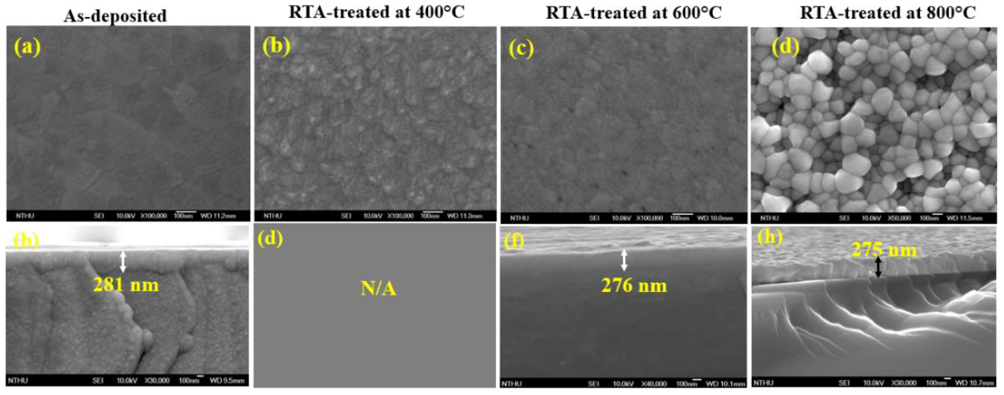
Figure 2.
The AFM surface topography images of (a) as–deposited, (b) RTA-treated at 400°C (c) RTA-treated at 800°C and (d) RTA-treated at 800°C ITO thin film. The surface with scallling of particle size of (e) as–deposited (f) RTA-treated at 400°C, (g) RTA-treated at 600°C and (h) RTA-treated at 800°C ITO thin film.
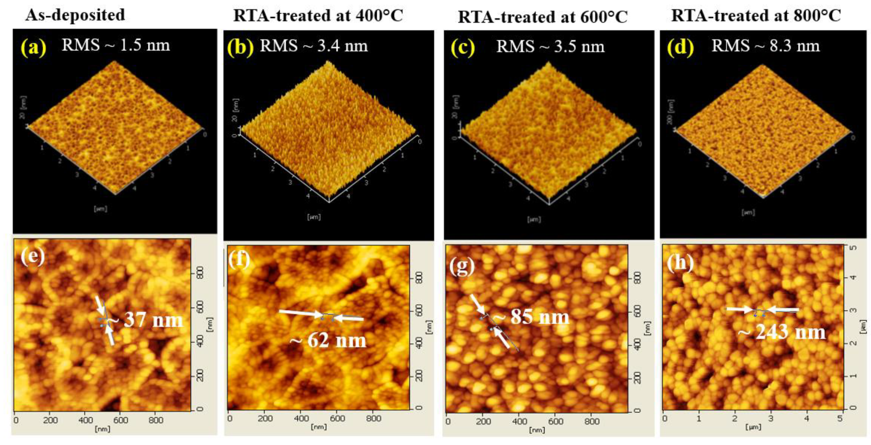
Figure 3.
Element analysis of (a) as-deposited (b) RTA-treated at 600°C and (c) RTA-treated at 800°C ITO thin film.
Figure 3.
Element analysis of (a) as-deposited (b) RTA-treated at 600°C and (c) RTA-treated at 800°C ITO thin film.
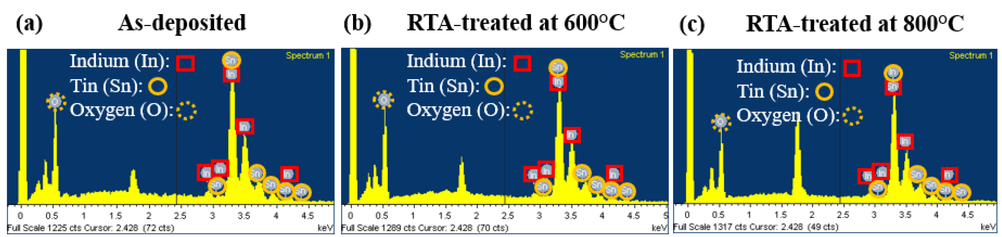
Figure 4.
THz (a) temporal waveforms and (b) amplitude spectra transmitted through bare HR silicon, as-deposited, RTA-treated 400°C, RTA-treated 600°C and RTA-treated 800°C ITO thin films. Inset in (b) shows phase linearity of the THz signal transmitted through a ITO /HR-Si annealed at 800°C.
Figure 4.
THz (a) temporal waveforms and (b) amplitude spectra transmitted through bare HR silicon, as-deposited, RTA-treated 400°C, RTA-treated 600°C and RTA-treated 800°C ITO thin films. Inset in (b) shows phase linearity of the THz signal transmitted through a ITO /HR-Si annealed at 800°C.
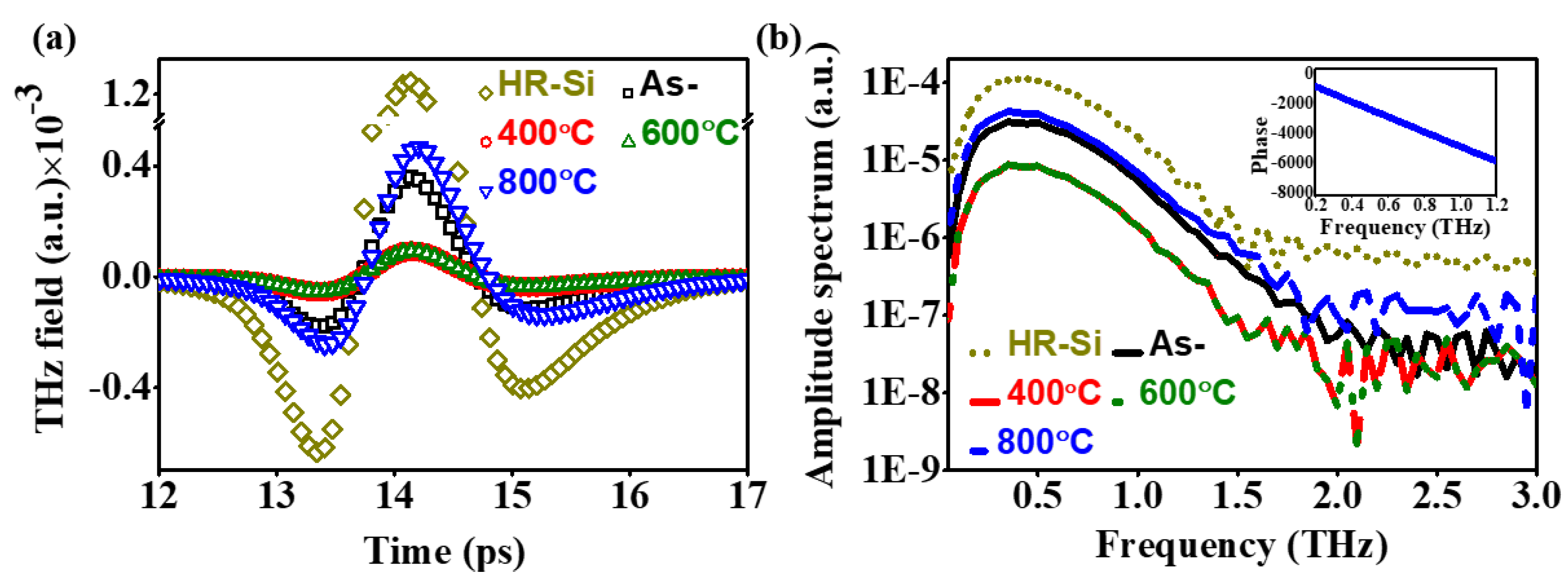
Figure 6.
THz frequency dependent (a) transmittance (b) absorbance and (c) reflectance of as-deposited, RTA treated at 400°C, RTA treated at 600°C and RTA treated at 800°C ITO thin film.
Figure 6.
THz frequency dependent (a) transmittance (b) absorbance and (c) reflectance of as-deposited, RTA treated at 400°C, RTA treated at 600°C and RTA treated at 800°C ITO thin film.
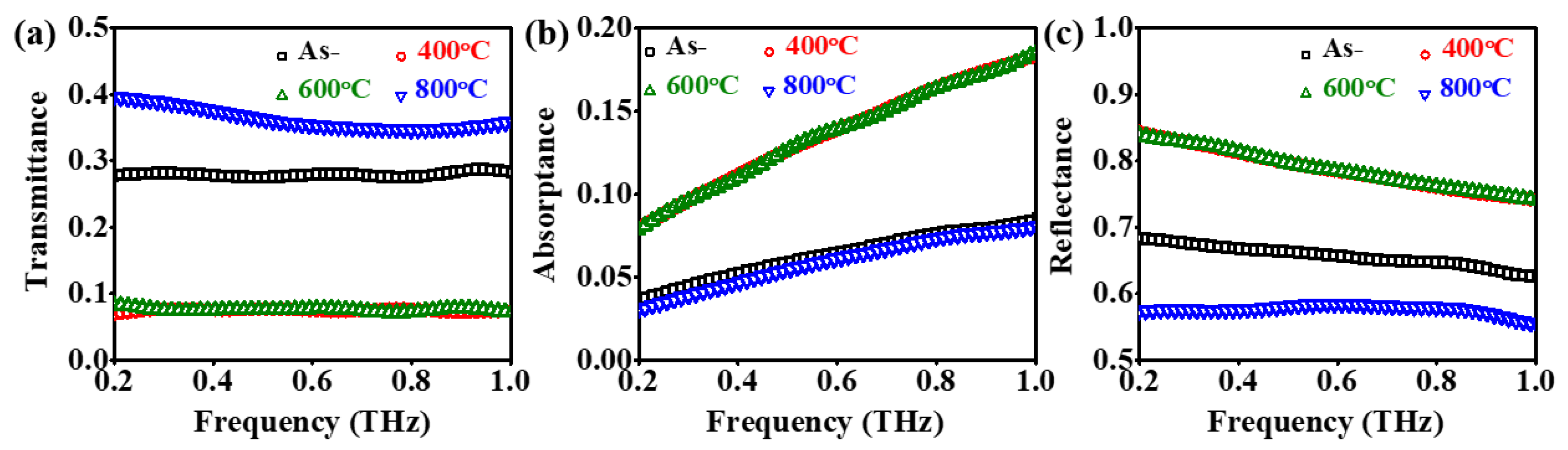
Figure 7.
(a) The real (σreal) and (b) imaginary ((σimg) part of conductivities as the function of THz frequencies of various ITO films. Solid and open circles are experimentally extracted conductivities The dashed curves are fitting lines using both models.
Figure 7.
(a) The real (σreal) and (b) imaginary ((σimg) part of conductivities as the function of THz frequencies of various ITO films. Solid and open circles are experimentally extracted conductivities The dashed curves are fitting lines using both models.
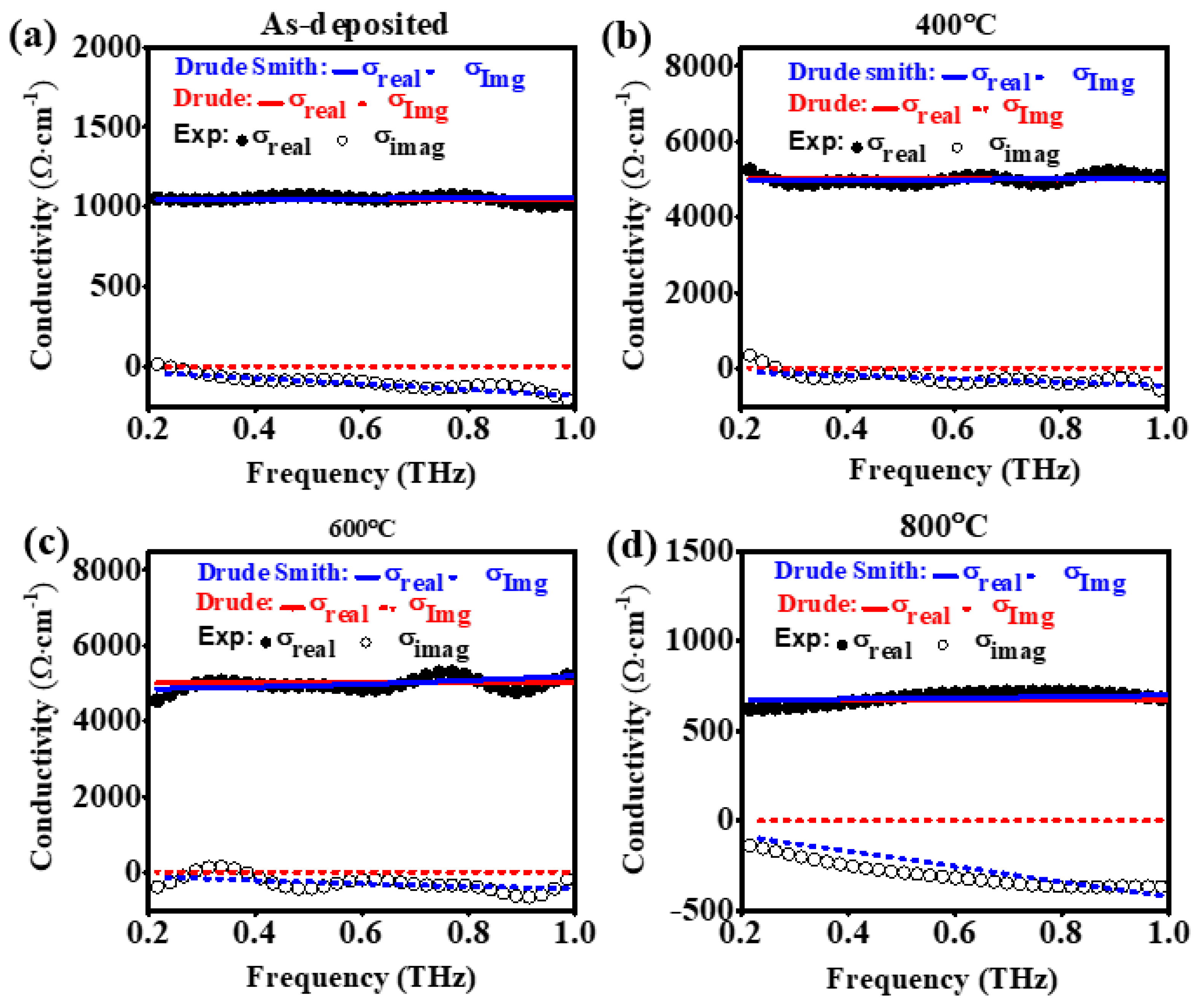
Figure 8.
(a) The transmittance and (b) reflectance and of as-deposited, RTA-treated at 400°C, RTA-treated at 600°C and RTA-treated at 800°C ITO thin film coated on fused silica as well T and R of fused silica (c) in UV-VIS-NIR region. .
Figure 8.
(a) The transmittance and (b) reflectance and of as-deposited, RTA-treated at 400°C, RTA-treated at 600°C and RTA-treated at 800°C ITO thin film coated on fused silica as well T and R of fused silica (c) in UV-VIS-NIR region. .
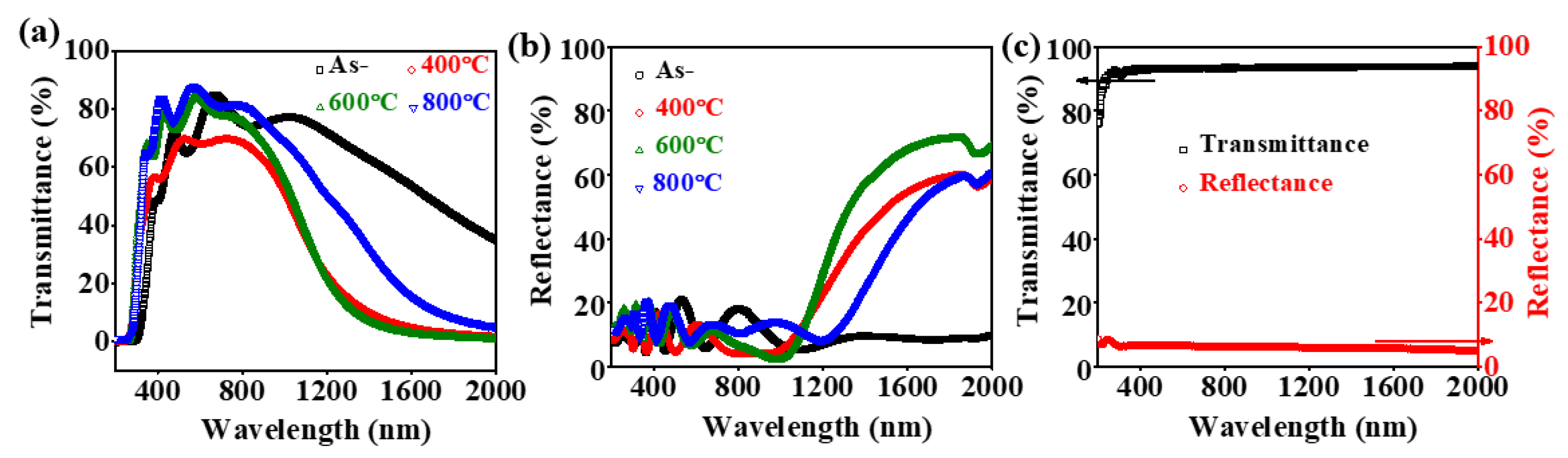
Figure 9.
(a) real (n) and (b) imaginary (κ) refractive index of as-deposited, RTA-treated at 400°C, RTA-treated at 600°C and RTA-treated at 800°C ITO thin film. .
Figure 9.
(a) real (n) and (b) imaginary (κ) refractive index of as-deposited, RTA-treated at 400°C, RTA-treated at 600°C and RTA-treated at 800°C ITO thin film. .
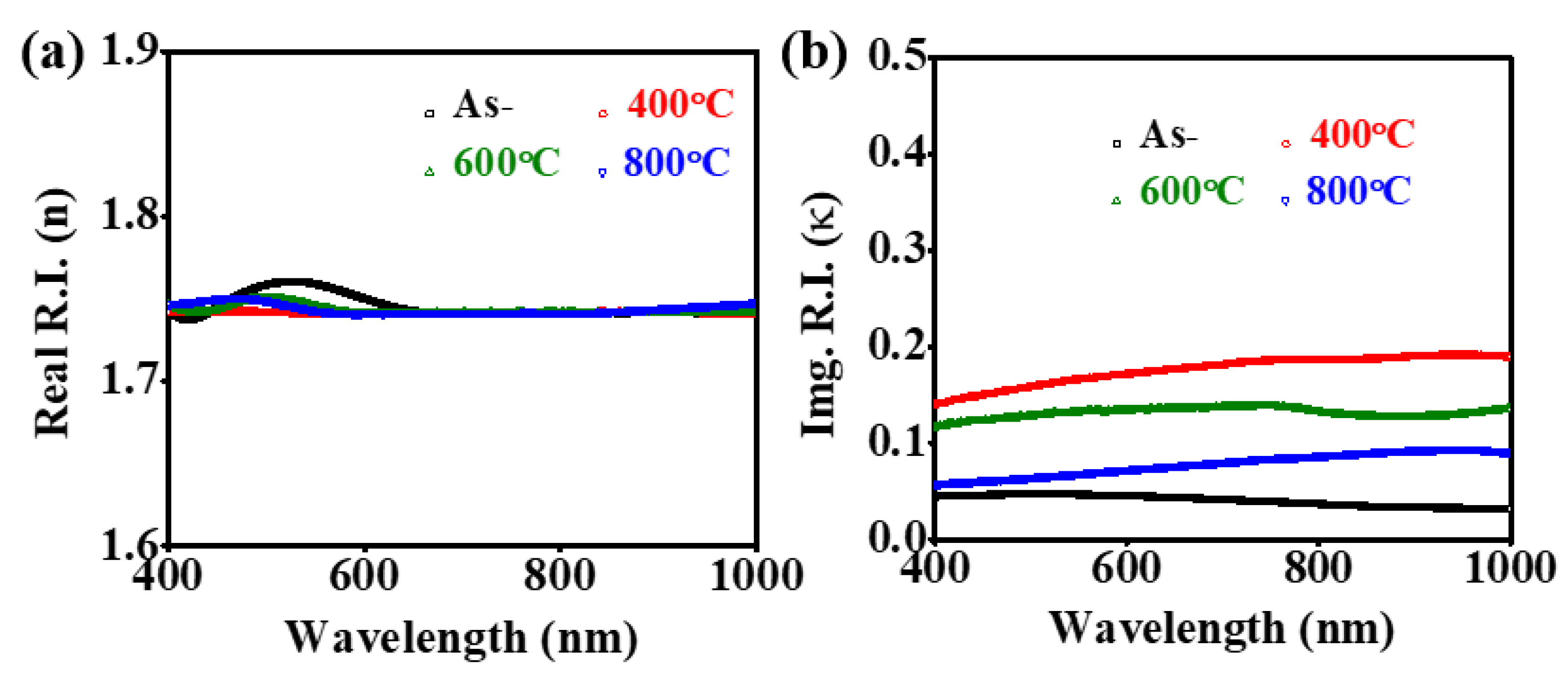
Figure 10.
The (a) wave-length dependent refractive index and (b) optical bandgap of as-deposited, RTA-treated at 400°C, RTA-treated at 600°C and RTA-treated at 800°C ITO thin film. .
Figure 10.
The (a) wave-length dependent refractive index and (b) optical bandgap of as-deposited, RTA-treated at 400°C, RTA-treated at 600°C and RTA-treated at 800°C ITO thin film. .
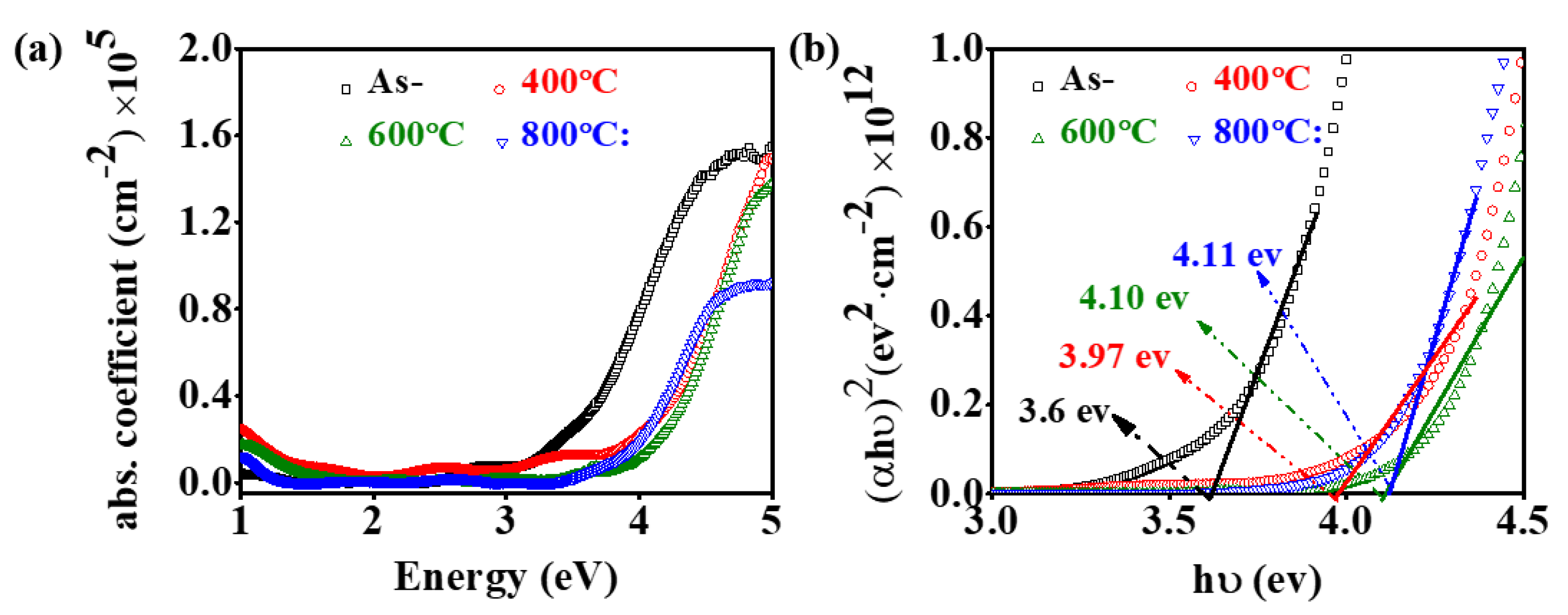

Table 1.
Element weight and atomic percentage analysis of as-deposited (denoted by As-), RTA-treated at 600°C (denoted by 600°C) and RTA-treated at 800°C (denoted by 800°C) ITO thin film.
Table 1.
Element weight and atomic percentage analysis of as-deposited (denoted by As-), RTA-treated at 600°C (denoted by 600°C) and RTA-treated at 800°C (denoted by 800°C) ITO thin film.
| Sample | O K | In L | Sn L | |||
| Weight (%) | Atomic (%) | Weight (%) | Atomic (%) | Weight (%) | Atomic (%) | |
| As- | 22.78 | 68.01 | 67.44 | 28.05 | 9.77 | 3.93 |
| 600°C | 22.98 | 68.23 | 69.48 | 28.75 | 7.54 | 3.02 |
| 800°C | 24.71 | 70.27 | 66.90 | 26.51 | 8.38 | 3.21 |
Table 2.
The electrical parameters of as-deposited (specified as As-), RTA-treated at 400°C (specified as 400°C), RTA-treated at 600°C (specified as 600°C) and RTA-treated at 800°C (specified as 800°C) ITO thin films.
Table 2.
The electrical parameters of as-deposited (specified as As-), RTA-treated at 400°C (specified as 400°C), RTA-treated at 600°C (specified as 600°C) and RTA-treated at 800°C (specified as 800°C) ITO thin films.
| Parameters | As- | 400°C | 600°C | 800°C |
|---|---|---|---|---|
| µ (cm2/V∙s) | 29 | 110 | 226 | 70 |
| ωp (rad·THz) | 3315 | 3711 | 2580 | 1648 |
| τ (fs) | 6 | 12 | 21 | 20 |
| c | -0.83 | -0.68 | -0.63 | -0.87 |
| N (cm-3) | 2.17×10²⁰ | 2.72×10²⁰ | 1.31×10²⁰ | 5.58×10¹⁹ |
| σ ( Ω-1‧cm-1) | 1019 | 4897 | 4881 | 628 |
| ρ (Ω‧cm) | 9.8×10⁻⁴ | 2.0×10⁻⁴ | 2.0×10⁻⁴ | 15.9×10⁻⁴ |
Disclaimer/Publisher’s Note: The statements, opinions and data contained in all publications are solely those of the individual author(s) and contributor(s) and not of MDPI and/or the editor(s). MDPI and/or the editor(s) disclaim responsibility for any injury to people or property resulting from any ideas, methods, instructions or products referred to in the content. |
© 2024 by the authors. Licensee MDPI, Basel, Switzerland. This article is an open access article distributed under the terms and conditions of the Creative Commons Attribution (CC BY) license (https://creativecommons.org/licenses/by/4.0/).
Copyright: This open access article is published under a Creative Commons CC BY 4.0 license, which permit the free download, distribution, and reuse, provided that the author and preprint are cited in any reuse.


