Submitted:
13 May 2024
Posted:
13 May 2024
You are already at the latest version
Abstract
The electric vehicle (EV) industry challenges battery joining technologies by requiring higher energy density both by mass and volume. Improving the energy density via new battery chemistry would be the holy grail but is seriously hindered and progresses slowly. In the meantime, alternative ways, such as implementing more efficient cell packaging by minimizing the electrical resistance of joints are of primary focus. In this paper we discuss the challenges associated with the electrical characterisation of laser soldered joints in general, and the minimization of their resistive losses, in particular. In order to assess the impact of the joint resistance on the overall resistance of the sample, the alteration in resistance was monitored as a function of voltage probe distance and modelled by finite element simulation. The experimental measurements showed two different regimes: one far from of the joint area and another in its vicinity and within the joints cross section. The presented results confirm the importance of the thickness of the filler material, the effective and the total soldered area, and the area and the position of the voids within the total soldered area in determining the electrical resistance of joints.
Keywords:
laser soldering
; filler material
; lap geometry
; electrical measurement
; numerical modelling
1. Introduction
Electric vehicles (EVs) have gained significant attention as green and environmentally friendly alternatives to vehicles driven by internal combustion engines [1,2,3,4]. A key component driving the propulsion of EVs is the battery pack, which stores and supplies electrical energy to power the vehicle’s electric motor. Battery packs play a critical role in determining the driving range, performance, and overall environmental impact of both full electric and hybrid vehicles [5,6,7,8]. As the demand for EVs continues to rise, there is a pressing need to increase the energy storage capacity of the battery pack, as well as to optimize its design, efficiency, and packaging [9,10].
While novel battery chemistry presents a promising long lasting avenue to meet the needs of vehicle manufacturers, its transformative impact is hindered by the intrinsic limitations of time-intensive development [11,12]. Considering this, a complex strategy is outlined that involves all aspects that maximize the extractable energy from the cells/battery packs making use of current battery chemistry [13]. Central to this strategy is the smart management of losses encountered during cell interconnections [14,15]. The reduction of such losses bears significant potential and may/can substantially contribute to overall efficiency. The extent of energy loss is primarily determined by the resistance of individual joints, that makes it essential to both accurately characterize and minimize these resistive losses. Therefore, the development of two things is important: a sturdy, well-controlled and reproducible joining process and an appropriate resistance measurement methodology for at least comparative purposes.
In recent years, from the plethora of potential joining technologies, laser-based welding, soldering and brazing emerge as particularly promising alternatives to traditional bonding methods, offering potential for producing high-quality joints. Laser-assisted filler-based joining techniques, such as soldering and brazing, have even surpassed laser welding in terms of electrical properties [16,17]. Brand et al. showed that soldered joint exhibited the lowest resistance as compared to other joining technologies, such as resistance, ultrasonic, and laser welding [17].
On the other hand, the electrical characterization of joints in overlap geometry created by any techniques is a challenging task in itself, and no standardized methods are currently available to meet these. On most occasions the four-point probe method, also known as the Kelvin or van der Pauw method is the most favourable option [16,17,18,19,20,21], as it offers a robust approach for resistance measurement that is also capable to mitigate measurement errors introduced by contact and lead wire resistances. The four-point probe method enables precise determination of the joint’s resistance while minimizing the impact of parasitic resistances, resulting in highly accurate and reproducible measurements [18]. However, the measurement probes are unable to distinguish between the resistance of the joint and the resistance of the base sheets to be joined, regardless of how close they are brought to the joint interface. In the literature the four-point probe method with several distances between the needle-tipped probes was used. Schmidt et al. and Schmalen et al. used 21 mm as a distance between the probes [16,17,20], while 16.5 mm or 11 mm distance was used by Biele et al. [18] and Hollatz et al. [21], respectively. The method, performed at one fixed measurement distance, is perfectly suitable for comparing the electrical characteristics of different samples, however, it cannot give exact values for the joint, instead it provides the cumulative resistance of the base plates and the filler together.
We could not find any report describing in-depth analysis of the electrical characteristics of laser soldered connections. Drawing upon all the information currently available in the literature, we suggest using laser soldering as a joining technology for battery connection and our approach is to find an evaluation strategy that is capable to provide the critical parameters of the electrical behaviour of these joints. Therefore, in this paper we report on electrical measurements of laser soldered DC01 and Hilumin® sheets, by monitoring the resistance as a function of the spatial distance between the two voltage probes. In addition to the experimental results, this study incorporates results obtained in COMSOL Multiphysics [22] environment, to enhance the understanding of the electrical behaviour of the connected sheets.
2. Materials and Methods
Joints were established between two types of steel sheets, specifically DC01 steel sheets measuring 0.5 mm in thickness, 15 mm in width, and 30 mm in length, and Hilumin® sheets with a thickness of 0.15 mm, a width of 9 mm, and a length of 30 mm. Hilumin® is a protected trademark of Tata Steel, for sheets specifically developed for battery applications and is a widely preferred material of the caps of cylindrical cells. It is made by electroplating a cold-rolled battery quality steel (DC04) with a nickel layer of several micrometer thickness with a final diffusion annealing step, that results in low contact resistance and high corrosion resistance [23].
The joint configuration chosen for our study was the overlap geometry, since it represents well the ”cap to cap”, the “bus bar to bus bar” and "battery cap to bus bar" joint types and hence responsible for the majority of the joints commonly employed in the assembly of a battery pack. To facilitate the connection of the two steel sheets, a homemade jig was used to clamp the plates together. Soldering was employed using a tin-based filler (Sn99.3Cu0.7), positioned between the two steel pieces, as illustrated in Figure 1. The filler material was also used in form of sheets, with a thickness of 0.16±0.01 mm and a width of 5.0±0.1 mm. To investigate the effect of filler amount, the length of the filler sheet was varied between 2.0 and 10.0 mm in the case of DC01 samples, and between 0.5 and 4.0 mm in the case of Hilumin® samples. It is important to note that the chosen tin-based filler had a liquidus temperature of 227 °C and incorporated a rosin-based flux to ensure proper wetting of the soldered surfaces [24]. Before fixing the sheets into the jig both steel sheets were roughened with p1200 sandpaper and precleaned with acetone rinsing.
A continuous-wave Yb-doped fiber laser (Model SP-400C-0005, SPI Lasers plc (currently Trumpf)) was utilized as the heat source. The laser emits a maximum power of 400 W at the central wavelength of 1071 nm and exhibits an almost perfectly Gaussian beam with an M2 value of approximately 1.08. The laser beam was directed onto the sample surface at an angle of incidence of approximately 10° in order to avoid the back reflection of the laser light into the cavity. For the soldering process, a glass lens with a focal length of 1000 mm was utilized to produce an illuminated spot in convergent laser beam phase on the upper surface of the sheet pair creating a slightly elliptical irradiation spot with a minor axis of ~4.5 mm, defined by the 1/e2 intensity criterion. To measure the laser power in situ, a photodiode (Thorlabs S130C) sampled a small portion of the processing laser beam to facilitate accurate and real-time power measurements during the experiments.
For measuring the electrical resistance of the joints the four-point probe measurement geometry was used: the current was fed by a TTi CPX200 power supply at the ends of the plates to be joined at a distance of 100 mm, and the voltage drop was measured across two internal probes by a Keithley 2401 multimeter so that the geometric center of the joint coincided with the middle point of the voltage measurement distance as depicted in Figure 2. This method is perfectly suitable for comparing the electrical characteristics of different samples if the distance of the internal electrodes is kept constant. However, it does not give exact values for the joint, instead it provides a cumulative resistance. Therefore, the measurement distance was varied between 1 and 81 mm in this study.
One way to accurately determine small resistances is to use large test currents in order to produce a voltage drop that can be measured with sufficient accuracy. As an example, to determine a 15 µΩ resistance with 1 % measurement error a current of at least 180 A is required [25]. However, such high currents are likely to cause a temperature rise within the samples that will affect the resistance, and ultimately may even cause damage in the structure of the joint. Therefore, we needed an alternative solution for precisely measure the resistance of the laser produced joints. One possible solution, coined asymptotic method, is where the resistance of the joint is measured at several current values and the resistance is plotted as a function of current. Here, the resistance is the limiting resistance value to which this R(I) curve approaches. Another approach, the so called slope method is more accurate. Here the potential drops are measured at several currents, and the slope of the U(I) curve provides the resistance of the joint. An additional advantage of the latter method is that it is “self-checking”: if all points fit well to a straight line, it proves that during the measurement none of the applied currents cause temperature rise in the system, i.e. the resistance is constant. Therefore, all resistance values reported here were measured by the slope method after carefully tested the linearity of the individual U(I) datasets. 10 A was set as the maximum current value that allowed measurements without any noticeable temperature rise during the 1-2 second measuring time. We found that for keeping the error of the resistance values below 1% (please note it is too small to be visible in Figure 3) measuring at 6 measurement points were necessary in the 0.1-10.0 A current range. Therefore, we derived joint resistances by measuring the potential drops at 0.1, 0.5, 1.0, 3.0, 6.0 and 10.0 A currents.
Our experimental investigations were complemented with numerical modelling. By developing a model in COMSOL Multiphysics, we gained insight into the distribution of current density and electric potential (by which the resistance can be calculated) within and in the vicinity of the soldered joint, facilitating a deeper understanding of the electrical characteristics of the interconnected sheets. Here the challenge is how well the COMSOL model describes the real joint in terms of its structure (e.g. electric transfer at the interfaces) and the materials property of the relevant component (sintered metal sheets or resolidified solder). The computational framework COMSOL Multiphysics version 5.5 was used for integrating three key modules, including the CAD Import Module, Library Material, and AC/DC Module. The accurate representation of the material behaviour was realized through the measurement and subsequent integration of pertinent electrical properties into the model. Notably, the foundational material for these properties was established based on the predefined “iron” and “Sn – 1 Cu” tin-based filler material from the Library Material module, thereby ensuring a robust and consistent starting point. To achieve a high level of accuracy and resolution in our simulations, the predefined “extremely fine” mesh was employed throughout the computational calculations.
3. Results and discussion
For assessing the impact of joint resistance on the net resistance of the sample, a thorough investigation was conducted. Instead of deriving the resistance at one fixed probe distance, the resistance, R was monitored as a function of the spatial distance between the two voltage probes (to be denoted as voltage probe distance, d).
The analysis of these R(d) curves exhibited two zones (cf. Figure 2) according to the different dependence of the resistance on the voltage probe distance. The boundary line between these two zones correlated well with the edge of the joining area, i.e. the perimeter within which resolidified filler was present after separating the joint sheets. Figure 2 proves convincingly the spatial distinction between the far and near zones. In the far zone (indicated by the blue lines in Figure 2), the measurement probes were positioned outside of the joining area. On the other hand, the near zone (marked by the red line in Figure 2) encompassed measurements conducted within the joining area. In Figure 3. the near and far zones are distinguished by full and dashed lines.
The net resistance as a function of the voltage probe distance at several different filler material volumes are shown in Figure 3a,b for the DC01 and Hilumin® samples, respectively. The DC01 samples were processed with 120 W laser power at 5 s irradiation time, while the Hilumin® samples were joined with 80 W laser power at 5 s.
Both material series exhibit comparable trends, thereby we elaborate upon the properties primarily within the context of the DC01 series. Across all soldered samples in the series, a consistent pattern emerges where the resulting resistance is consistently lower than that of the base material. A distinction in R(d) relationship is apparent between the near and far zones. Moreover, a nearly linear correlation between the resistance and the voltage probe distance is discerned within both individual zones. Furthermore, this linearity persists regardless of the quantity of filler material used. It is also clear that every R(d) curve breaks between 9 and 12 mm and 6 and 9 mm for DC01 and Hilumin® respectively. These break points correlate with the diameter of the effective soldered area. Nevertheless, the slope and the intercept of these linear functions are dependent upon the volume of the filler material as it is shown in Figure 4. Notably, the dependencies from the volume do not follow a monotonous trend but rather these curves moved further and further away from the straight line of the base metal, i.e. they had a smaller intercept by increasing the amount of solder. This trend could be seen until the optimum amount of solder (indicated by arrows in the figure) is reached, after which it reversed. This behaviour is fully in line with morphological variation of the resolidified filler, reported earlier [26], namely that there is an optimal amount of solder for any laser power - irradiation time pair, where the filler completely melts and results in a joint that exhibits the most homogenous resolidified filler, i.e. the one which has the least amount of voids (due to bubbles) and/or solid remnants. This optimum is 4.8 mm3 and 1.6 mm3 for the DC01 and Hilumin® sets, respectively, under the process conditions applied. While the trends are congruent, differentiation arises in the parameter values that define the linear relations encapsulating the electrical behaviour between the DC01 and Hilumin® series. The variations in the slope and the intercept inherently distinguish the DC01 and Hilumin® material series, thereby support the fact that they have unique electrical properties.
4. Modelling and Discussion
Numerical simulations provide a valuable tool for studying complex phenomena and understanding the underlying physics of systems in a controlled virtual environment where experimental manipulation is challenging. By exploring comprehensively, the effect of factors such as material properties and filler material geometry, a three-dimensional finite element model was developed using the COMSOL Multiphysics® program.
To check the validity of the model, the distribution of the current density vectors over the contact area was determined first. The three-dimensional COMSOL model revealed that approx. 97% of the current flowed through the outermost, 10% part of the full contact area (Figure 5). This result is in line with the conclusion of a study of Brand et al. who described soldered joints with a simplified equivalent circuit model called resistance network with the characteristics given analytically in two dimensions [17]. As the next step, the effect of a filler of 1.6 mm3 volume on the electrical resistance of the joint was simulated for four different forms of the resolidified filler material, while effective bonding area kept constant, namely: cylindrical filler (Approx. 1.), cylindrical filler with one big void (Approx. 2.), cylindrical filler with a big void in an asymmetric position (Approx. 3.), and cylindrical filler with a big asymmetrical void and several smaller voids (Approx. 4.). Finally, the precise geometry of a real joint was modelled in 3D using the optical microscope image of the torn surface (Approx. 5.). These five models are depicted in Figure 6a) and the results of the simulated R(d) curves are shown in Figure 6b).
These numerical simulations predict a linear dependence of the resistance on the voltage probe distance (fully in line with the experimental behaviour presented in Figure 3.) in both near and far zones. It is also clear that every R(d) curve breaks at around 11 mm (except at Approx 1. where the diameter was 6.6 mm), i.e. the precise diameter of the inbounding circle used to describe the filler in the 3D model. However, there is a deviation between the measured and simulated R(d) curves: the calculated R values are continuously smaller and larger than the measured ones in the near and far zones, respectively. Moreover, the refinement of the geometrical fidelity of the resolidified filler (through Approx. 1. to 5.) results in simulated R values that approach the measured ones (plotted in solid lines) from below and above, in the near and far zones, respectively (indicated by the blue arrows). Near and far linearities are not depending on the geometry of the filler, while the role of the geometry is decisive in the accuracy of the specific resistance values. Furthermore, the approximations resulted in bigger differences in resistance in the near zone as compared to the far zone.
Experimenting with these numerical simulations and especially with the different approximation models proved that five geometrical properties of the filler material influenced the electrical characteristics, namely the thickness of the resolidified filler material between the two sheets, h, the area where the two metal sheets are joined by the filler, referred to as effective soldered area, Aeff, the total area of voids, Avoid, the total joint area, Atotal, which is the sum of the effective soldered area and the area of the voids, and finally the position of the voids within the total soldered area. In the following the effect of these five parameters on the linear functions in the near and far zones is shown for the case of connecting the two DC01 stripes with a filler of 1.6 mm3 volume. The reason for choosing this case was, that among the samples of different volumes of filler this one contained the most voids, hence being the most appropriate to model the effect of the void area and the effect of their distribution. Five cases were considered:
- Case I: The thickness of the resolidified filler material was varied, while we kept the filler volume constant (tfiller=varied, Vfiller=constant).
- Case II: The effective soldered area was varied without the presence of voids (Aeff=varied, Avoid=0).
- Case III: The total joint area was kept constant, while its two components, i.e. the effective soldered are and the void area were varied (Atotal=Aeff+Avoid=constant, Avoid/Atotal=varied).
- Case IV: The effective soldered area was fixed, while varying the void area, which resulted in the variation of the total soldered area (Avoid=varied, Atotal=varied, Aeff=constant).
- Case V: The distribution of voids, i.e. their location was shifted within the total soldered area (Atotal=constant, Avoid=constant, posvoid=varied).
5. The effect of Characteristics of the Soldered Joint on the R(d) Function
In order to determine the effect of the soldered joints on the characteristics of the R(d) plots, the simulated parameters were changed from -50% to +50% relative to the measured value of each parameter (except the Case V). Table 1. summarizes the experimentally obtained values of each and every parameter of the soldered joint listed above, together with their respective ranges in which we varied their values in the simulations.
The relative changes of the minima to the maxima of the slopes were expressed in percents, with the following equation:
where X stands for the slopes (sf, sn) or the intercepts (if, in) in the far and near zones. The negative or the positive sign of the relative change indicates that when the simulated parameter increases (i.e. from -50% to +50% of the measured value) the calculated slopes move away from or closer to the measured characteristics respectively. The varying the property resulted in monotone changes in each and every cases. Two types of changes were distinguished: linear and reciprocal.
The distance dependence of the resistance, R(d) is a linear function that will be described in the following form for both the near and far zone:
where sx and ix denotes the slope and the intercept of the straight line, and x index can be f for far and n for near zone.
5.1. The Far Zone
The relative changes of the slopes for different cases in the far zone are shown in Figure 7. The magnitude of the relative changes is small (i.e. less than 0.65% in all cases), none of the parameters varied has substantial impact on the slope in the far zone.
Previously we concluded that the measured slope in the far zone was the same for all amounts of filler materials but differed between the DC01 and Hilumin® samples. This observation was consistent with the conclusion that the far-zone slope was determined by the material of the sheets to be joined. This point was double-checked by measuring the slope of the R(d) curves in the far zone with different metal sheets. It can be demonstrated algebraically that:
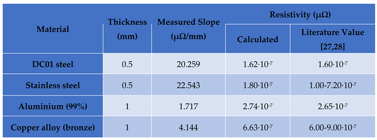
The experimentally determined resistivity values derived from the measured slopes and the cross section of the sheets, exhibit a close correlation to the values reported in the literature as summarized in Table 2. Therefore, we conclude that the slope of the R(d) curves in the far-zone is related to the resistivity of the material to be joined.
We double-checked the effect of the cross-section of these sheets on the far zone slope of the R(d) functions, as well. When the width of the sheet was halved, then the slope was increased by two times. Therefore, the slope in the far zone, sf can be described by the following formula:
where ρDC01 is the electrical resistivity of the sheet’s material and ADC01 is the cross-section of the metal sheets to be joined. Therefore, the final conclusion is that the slope in the far zone is determined by the electrical resistivity and the cross-section of the material to be joined.
The results of simulations, expressed as relative changes, that refer to the behaviour of the intercepts in the far zone are shown in Figure 8. The intercepts are dominantly determined by the effective soldered area (Case II), and the total joint area (Case IV). These two parameters have five times larger effect on the intercept than any of the other three parameters. The calculated intercepts derived from the differences between the resistance of the sheet and the respective joints measured at 21 mm are displayed as a function of the effective soldered area in Figure 9. The intercepts are decreasing with increasing effective soldered area and change sign at approx. 15 mm² soldered area. The rate is most significant in the 0-25 mm2 area domain, flattens off at and above 60 mm2 ultimately approaching an intercept value of approx. -150 µΩ. These results in line with the model calculations reveal a reciprocal dependency from the effective soldered area with an exponent of 0.65 up to flattening:
An increase in the volume of the voids (Case III) is detrimental by increasing the resistance of the joint as demonstrated experimentally [26], appearing as a negative relative change in the intercept. These two effects dominated by effective soldered area (Case II) are combined in the impact of the total joint area (Case IV).
5.2. The Near Zone
In order to determine the effect of the five relevant geometrical properties of the filler material on the slope in the near zone, the parameters were changed similarly to those in the far zone. The relative effects observed in the five cases are shown in Figure 10.
In near zone the change of each and every property of the soldered joint causes a change of at least one order of magnitude greater than in the far zone. Among the five parameters examined, the void area (Case III) emerges as the most influential parameter in positive and the thickness (Case I) and the effective soldered area (Case II) in negative way i.e., whether the modelled points are closer or further away from the measured slope data points. These changes mean, that the addition of filler material and volume of voids results in an overall lower and higher resistance in the near zone respectively.
If we assume that the two sheets and the filler are connected in parallel, then:
where ρfiller is the electrical resistivity of the filler, and the c1 and c2 are coefficients that are related to the geometry of the sheets and the filler (cf. Figure 11):
While being formally similar to Eq 1. valid in the far zone, this definition of the slope by Eq. 3 is more universal since it combines the contribution of both the metal sheets and the filler material. In the far zone the voltage probe distance, d is much greater than the thickness of the filler and hence c1>>c2, the second term in Eq. 3 describing the slope in the near zone can be neglected. Therefore Eq. 3 can be taken as a universal definition of the slope that applies both in the near and far zones.
The results displaying the impact of the five relevant properties of the filler material's geometry on the intercept in the near zone are shown in Figure 12.
The model calculations give intercepts near to zero in Cases I and II when the presence of voids is not considered, i.e. Avoid=0. Since in these cases both the minima and the maxima are small absolute numbers, the relative changes in Cases I and II are small as well. The appearance of voids causes a huge change in the intercept of the R(d) curve in the near zone. In Cases III and IV the high maxima with near zero minima result in the high numbers shown in Figure 12. Simulations of the streamlines within the filler explained the immense effect of the presence of the voids: The reason for the great impact of the voids on the electrical characteristics of the joint is that each void acts as a source of return currents. In the vicinity of voids, the "return current" contributes to the elongation of the current path, thereby leading to an extended interaction of electrons with both the steel sheets and the filler material. Consequently, the resistance experiences an increase, significantly impacting the measured resistance-distance relationship in the near zone. Notably, under conditions of constant void quantity and distribution, the elongation of current paths resulting from these mechanisms remains uniform, thereby rendering it independent of the measurement distance (d). In the context of the R(d) function, this phenomenon thus influences the intercept rather than the slope. This effect is exemplified in the vicinity of a single void in Figure 13. where we display the norms of the current density vector, i.e. its magnitude, in the plane midway within the filler layer. In Figure 13c) current density values highlighted in the green circle represent the return current along the circumference of the void indicated by the red vertical dashed line. From the simulated results it follows, that the void area dependence of the intercept in the near zone can be described as:
Since in Case V both the + and – 50% values refer to the presence of voids, the relative change is not so impressive compared to Cases III and IV, nevertheless the distribution of the voids has a great influence on the intercept in the near zone.
6. Conclusions
This article focuses on the electrical resistance of laser-soldered joints, particularly on the challenges associated with the problems of the electrical characterisation in general, and minimization of the resistive losses in joints in particular. While the electrical characterization of joints in the overlap geometry is pivotal when assessing the performance of the joint, no standardized methods are currently available. The four-point probe method usually employed is ideal for comparative purposes, but it can’t provide exact values for the resistance of the joint.
In order to assess the impact of the joint resistance on the overall resistance of the sample, the resistance was monitored as a function of the spatial distance between the two inner probes, i.e. those used for voltage measurement. Two zones were distinguished: near and far zones, depending on whether the voltage probes are placed within, or outside the cross section of the soldered area. Measurements conducted in the far and near zones revealed linear relationships between the resistance and voltage probe distance. A modelling approach using COMSOL Multiphysics provided valuable insight into the complex phenomena and underlying physics. The simulations confirmed the importance of five parameters in determining the electrical resistance of joints, namely the thickness of the filler material, the effective and the total area, and the area and the position of the voids within the total joint area. The novel approach introduced here revealed how the geometry and the morphology of the bond formed by the resolidified filler material influenced the electrical characteristics of the joint.
The slopes derived in the far zone were determined by the electrical properties and the geometry of the material to be joined. In the near zone, the slopes decreased with an increase in the volume of filler material. Eq. 3 describes the slopes in both the far and near zones indicating that they are material specific, the former referring to the material to be joined, while the latter including both the sheets and the solder/filler material, while yielding no information about the electrical characteristics of the connection.
The intercepts of the straight lines in the far zone expressed in ohms indicate the difference in the resistance of the respective soldered structures as compared to that of the bare metal to be joined. The behaviour of the intercepts in the near zone also reflects the changes in the electrical characteristics of the joints due to the inhomogeneities in the number and distribution of the voids. Both intercepts compare the resistance of the couple as compared to the sheets, measuring the improvement due to the insertion of the soldered joint, allowing for a correct description of the synergy of the underlying processes.
In summary, this study contributes to the understanding of the effect of the material(s) to be joined and the characteristics of the solder in determining the electrical resistance behaviour in laser-soldered joints. Although the input data were obtained by laser soldering of metal sheets in the lap geometry, the derived tendencies are more universal and describe the slopes and the intercepts of the two linear regimes of the R(d) curves by 5 geometrical parameters of the resolidified solder. A key, but not the sole beneficiary of these results is the EV sector, where maximizing the efficiency and hence minimizing the losses of the battery pack could be a game-changer.
Author Contributions
“Conceptualization, A.K., G.Zs. and T.Sz.; methodology, A.K. and G.H.; software, A.K.; validation, A.K.; formal analysis, A.K.; investigation, A.K. and G.H.; resources, Zs.G..; data curation, A.K.; writing—original draft preparation, A.K.; writing—review and editing, Zs.G. and T.Sz.; visualization, A.K.; supervision, Zs.G. and T.Sz..; project administration, Zs.G.; funding acquisition, Zs.G. All authors have read and agreed to the published version of the manuscript.
Funding
This research was funded by EFOP-3.6.1-16-2016-00014 project, entitled “Research and development of disruptive technologies in the area of e-mobility and their integration into the engineering education.
Institutional Review Board Statement
This study did not require ethical approval.
Informed Consent Statement
This study did not involve humans.
Data Availability Statement
Data underlying the results presented in this paper (in the form of numeric data sets) are not publicly available at this time but may be obtained from the authors upon reasonable request.
Acknowledgments
The authors thank Edutus University for providing the laser source and other additional equipment for our experiments.
Conflicts of Interest
The authors declare no conflicts of interest.
References
- Poullikkas, A., 2015., Sustainable options for electric vehicle technologies. Renewable and Sustainable Energy Reviews, 41, pp. 1277–1287. [CrossRef]
- Leijon, J.; Boström, C., 2022., Charging Electric Vehicles Today and in the Future. World Electr. Veh. J. 13, 139. [CrossRef]
- Novas, N.; Garcia Salvador, R.M.; Portillo, F.; Robalo, I.; Alcayde, A.; Fernández-Ros, M.; Gázquez, J.A., 2022, Global Perspectives on and Research Challenges for Electric Vehicles. Vehicles, 4, 1246-1276. [CrossRef]
- Barkenbus, J.N., 2020., Prospects for Electric Vehicles., Sustainability, 12, 5813. [CrossRef]
- Verma, S., Mishra, S., Gaur, A., Chowdhury, S., Mohapatra, S., Dwivedi, G., Verma, P., 2021., A comprehensive review on energy storage in hybrid electric vehicle, Journal of Traffic and Transportation Engineering, Vol. 8, Issue 5, pp. 621-637. [CrossRef]
- Liu, W., Placke, T., Chau, K.T., 2022, Overview of batteries and battery management for electric vehicles, Energy Reports, Vol. 8, pp. 4058-4084. [CrossRef]
- Zeng, X., Li, M., Abd El-Hady, D., Alshitari, W., Al-Bogami, A. S., Lu, J., Amine, K., 2019, Commercialization of Lithium Battery Technologies for Electric Vehicles., Adv. Energy Mater. 9, 1900161. [CrossRef]
- Speirs, J., Contestabile, M., Houari, Y., Gross, R., 2014, The future of lithium availability for electric vehicle batteries, Renewable and Sustainable Energy Reviews, Vol. 35, pp. 183-193. [CrossRef]
- Li, Y. & Li, K. & Xie, Y. & Liu, B. & Liu, J. & Zheng, J. & Li, W., 2021, Optimization of charging strategy for lithium-ion battery packs based on complete battery pack model, Journal of Energy Storage, 37, 102466. [CrossRef]
- Zhuang, W., Liu, Z., Su, H., & Chen, G., 2021, An intelligent thermal management system for optimized lithium-ion battery pack. Applied Thermal Engineering, 189, 116767.. [CrossRef]
- Piątek, J., Afyon, S., Budnyak, T. M., Budnyk, S., Sipponen, M. H., Slabon, A., 2021, Sustainable Li-Ion Batteries: Chemistry and Recycling., Adv. Energy Mater., 11, 2003456. [CrossRef]
- Deng, D., 2015, Li-ion batteries: basics, progress, and challenges., Energy Sci Eng, 3: 385-418. [CrossRef]
- Fares, A., Klumpner, C., Sumner, M., 2019, Optimising the structure of a cascaded modular battery system for enhancing the performance of battery packs, The Journal of Engineering, 2019. [CrossRef]
- Zwicker, M. F. R., Moghadam, M., Zhang, W., Nielsen, C. V., 2020. Automotive battery pack manufacturing – a review of battery to tab joining. Journal of Advanced Joining Processes, Vol.1., 100017.. [CrossRef]
- Das, A., Ashwin, T.R., Barai, A., 2019, Modelling and characterisation of ultrasonic joints for Li-ion batteries to evaluate the impact on electrical resistance and temperature raise, Journal of Energy Storage, Volume 22, pp. 239-248. [CrossRef]
- Brand, M. J., Schmidt, P. A., Zaeh, M. F., Jossen, A., 2015.Welding techniques for battery cells and resulting electrical contact resistances, Journal of Energy Storage, Vol. 1, pp. 7-14. [CrossRef]
- Brand, M. J., Kolp, E. I., Berg, P., Bach, T., Schmidt, P., Jossen, A., 2017. Electrical resistances of soldered battery cell connections, Journal of Energy Storage Vol. 12, pp. 45–54.. [CrossRef]
- Persvik, Ø. & Zhang, Z., 2019, Four-point transient potential drop measurements on metal plates, Measurement Science and Technology, 31, 024006. [CrossRef]
- Biele, L., Schaaf, P., Schmid, F., 2021, Specific Electrical Contact Resistance of Copper in Resistance Welding, Phys. Status Solidi A, Vol. 218, Issue 19. [CrossRef]
- Schmalen, P., Plapper, P., 2017, Resistance Measurement of Laser Welded Dissimilar Al/Cu Joints, Journal of Laser Micro Nanoengineering. Vol. 12. No. 3. [CrossRef]
- Hollatz, S., Kremer, S., Ünlübayir, C., Sauer, D., Olowinsky, A., Gillner, A., 2020, Electrical Modelling and Investigation of Laser Beam Welded Joints for Lithium-Ion Batteries, Batteries. Vol. 6., No 24.. [CrossRef]
- COMSOL Multiphysics® Simulation Software, accessed May 2024. https://www.comsol.com/comsol-multiphysics.
- HILUMIN® ultra-clean nickel-plated steel, accessed May 2024. https://www.tatasteeleurope.com/engineering/products/electro-plated/hilumin-ultra-clean-nickel-plated-steel.
- Datasheet of lead free solder, FELDER GMBH Löttechnik, accessed May 2024. https://www.felder.de/files/felder/pdf/EN_18-ISO-Core_RA_lead-free.pdf.
- Schmidt, P. A., Schweier, M., Zaeh, M. F., 2012, Joining of lithium-ion batteries using laser beam welding: electrical losses of welded aluminum and copper joints, 31st International Congress on Applications of Lasers and Electro-Optics., pp. 915-923.
- Körmöczi, A., Horváth, G., Szörényi, T., Geretovszky, Zs., 2020, Laser assisted filler-based joining for battery assembly in aviation, SAE Int. J. Aerosp., Vol. 13, No. 2. [CrossRef]
- Serway, R. A., 1998, Principles of Physics (2nd ed.). Fort Worth, Texas; London: Saunders College Pub., ISBN 978-0-03-020457-9.
- Haynes, W. M., 2015, CRC Handbook of Chemistry and Physics (95th ed.). CRC Press, Taylor & Francis Group, Boca Raton, FL, ISBN 978-1-4822-0868-9.
Figure 1.
Schematic illustration of laser soldering of two metal sheets.
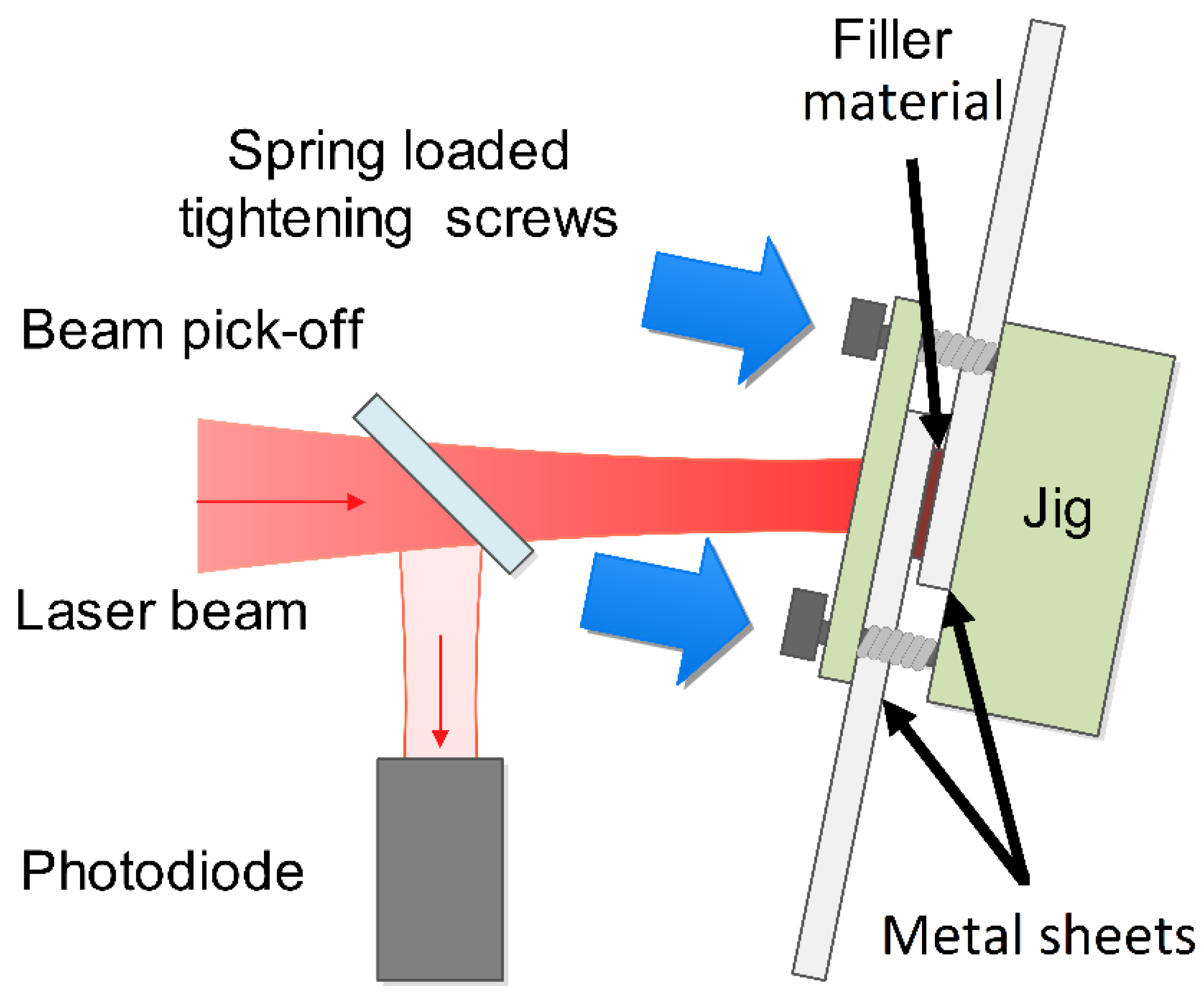
Figure 2.
Schematic illustration of the electrical measurement setup. Far and near zones are marked.
Figure 2.
Schematic illustration of the electrical measurement setup. Far and near zones are marked.
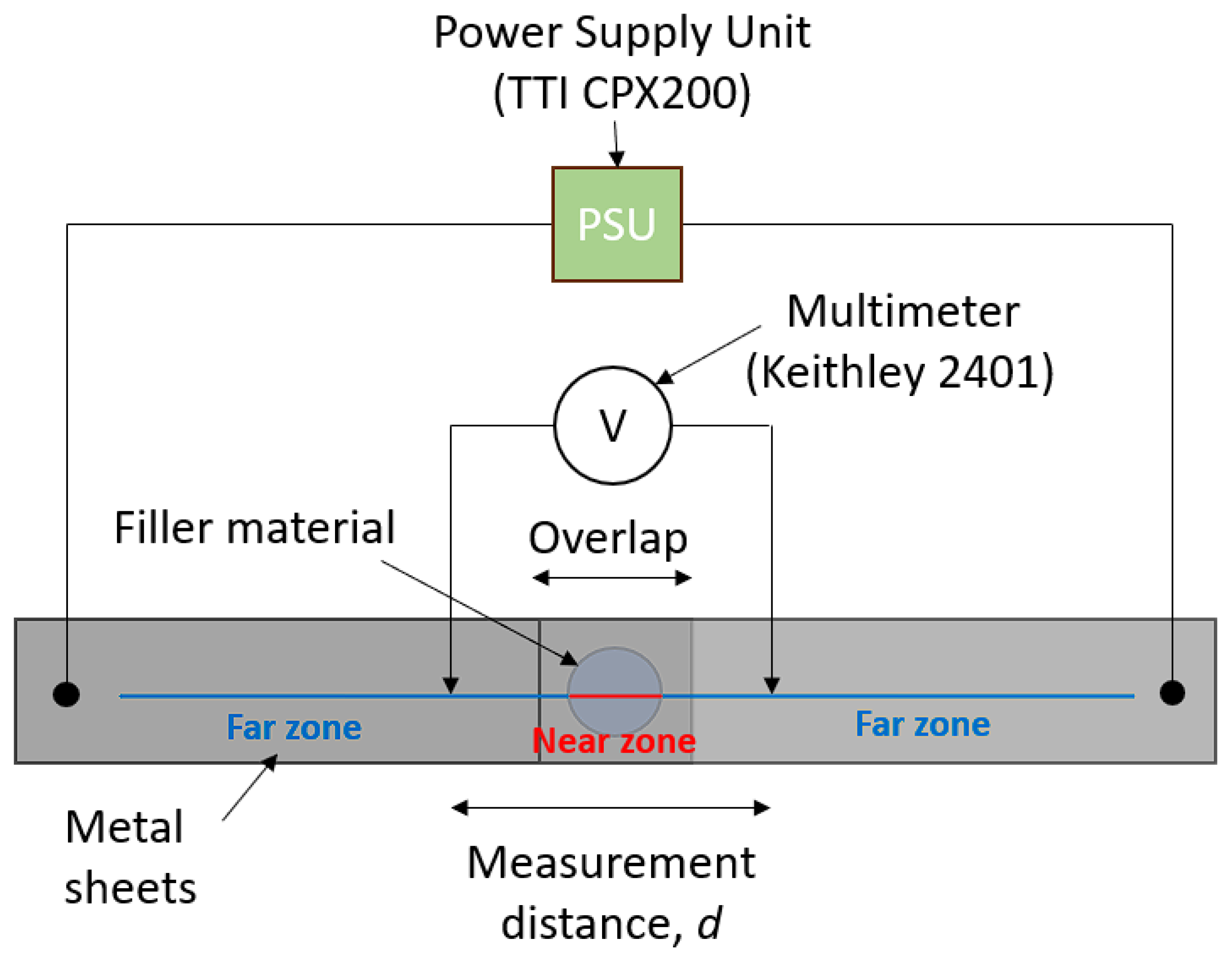
Figure 3.
Resistance as a function of voltage probe distance for different amounts of filler materials for a) DC01 and b) Hilumin® samples.
Figure 3.
Resistance as a function of voltage probe distance for different amounts of filler materials for a) DC01 and b) Hilumin® samples.
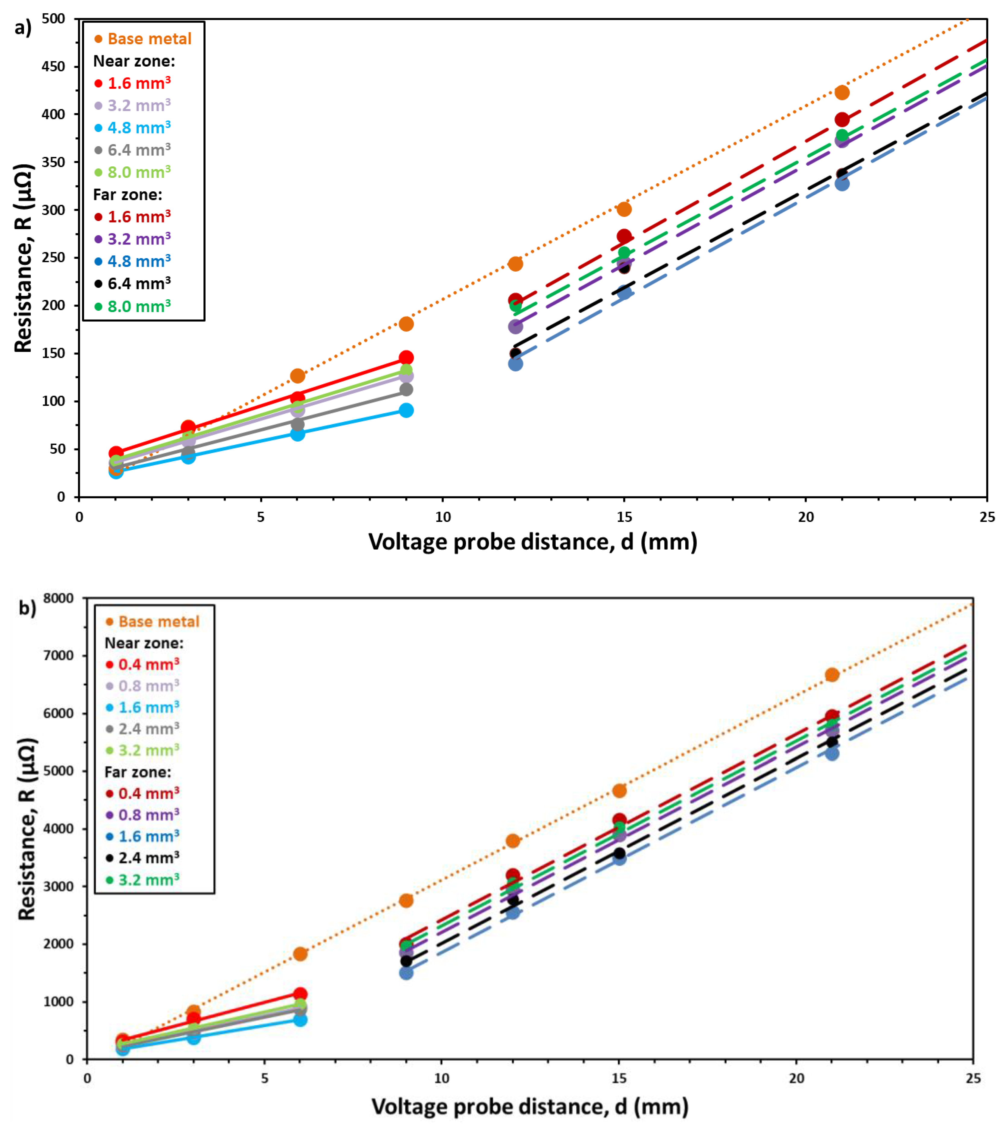
Figure 4.
Fitting parameters in far and near zone for DC01 (blue) and Hilumin® (red) sheets as a function of the volume of the filler material. The optimal filler volume is indicated by the arrows.
Figure 4.
Fitting parameters in far and near zone for DC01 (blue) and Hilumin® (red) sheets as a function of the volume of the filler material. The optimal filler volume is indicated by the arrows.
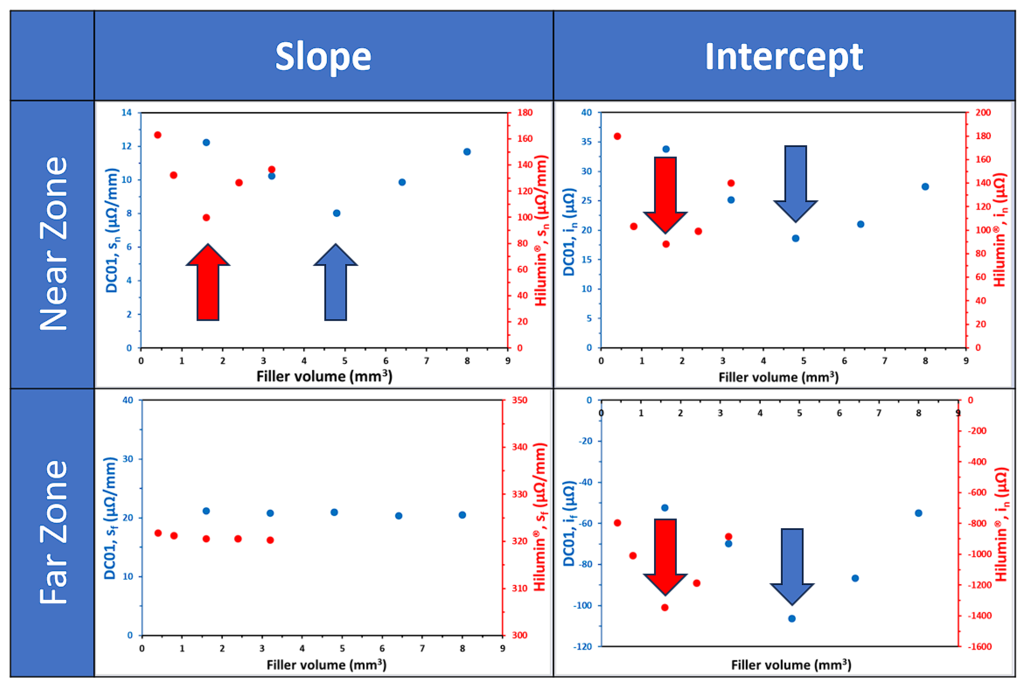
Figure 5.
The z component of the current density vectors in filler material at y=7.5 mm and z=0.53 mm section as shown in the inset.
Figure 5.
The z component of the current density vectors in filler material at y=7.5 mm and z=0.53 mm section as shown in the inset.
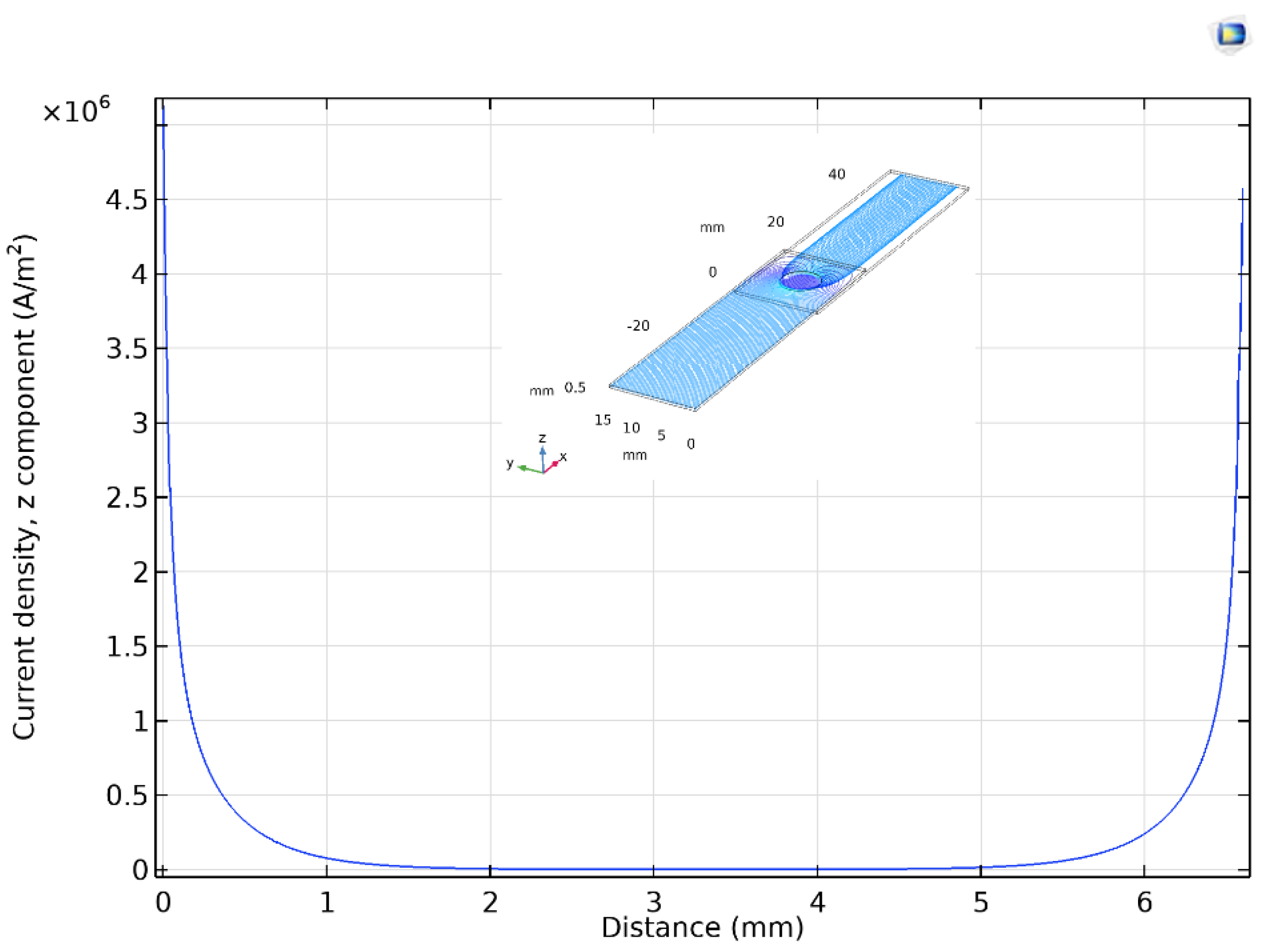
Figure 6.
a) Five different approximations of the real geometry of the resolidified filler material, and b) result of these approximations compared to a measured dataset (solid lines).
Figure 6.
a) Five different approximations of the real geometry of the resolidified filler material, and b) result of these approximations compared to a measured dataset (solid lines).

Figure 7.
The effect of variation of the five relevant properties of the soldered joint by ± 50% on the slopes in the far zone.
Figure 7.
The effect of variation of the five relevant properties of the soldered joint by ± 50% on the slopes in the far zone.
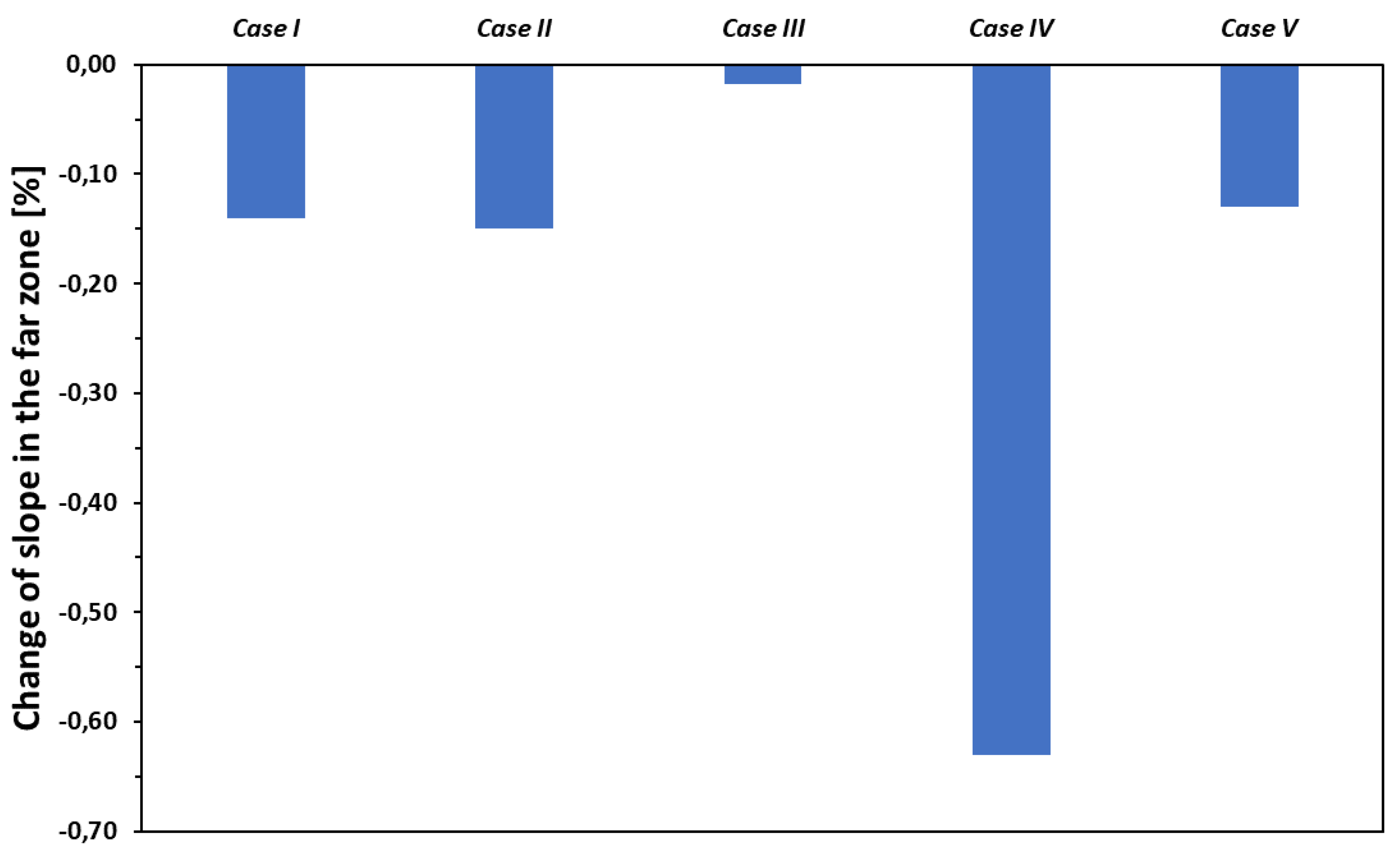
Figure 8.
The effect of changing the five relevant properties of the soldered joints by ± 50% on the intercept of R(d) in the far zone.
Figure 8.
The effect of changing the five relevant properties of the soldered joints by ± 50% on the intercept of R(d) in the far zone.
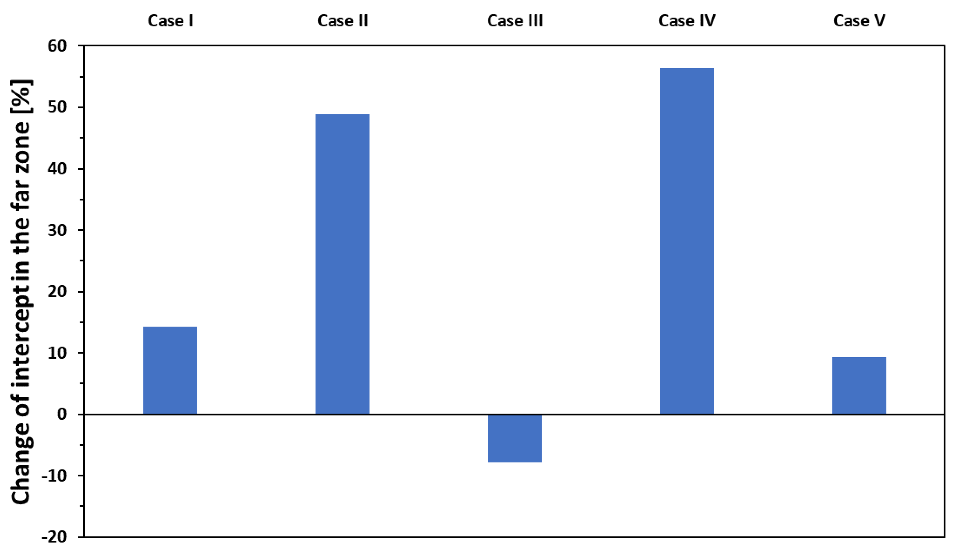
Figure 9.
The intercept of the R(d) in the far zone, as a function of effective soldered area (the voltage probe distance was set to 21 mm in this case).
Figure 9.
The intercept of the R(d) in the far zone, as a function of effective soldered area (the voltage probe distance was set to 21 mm in this case).
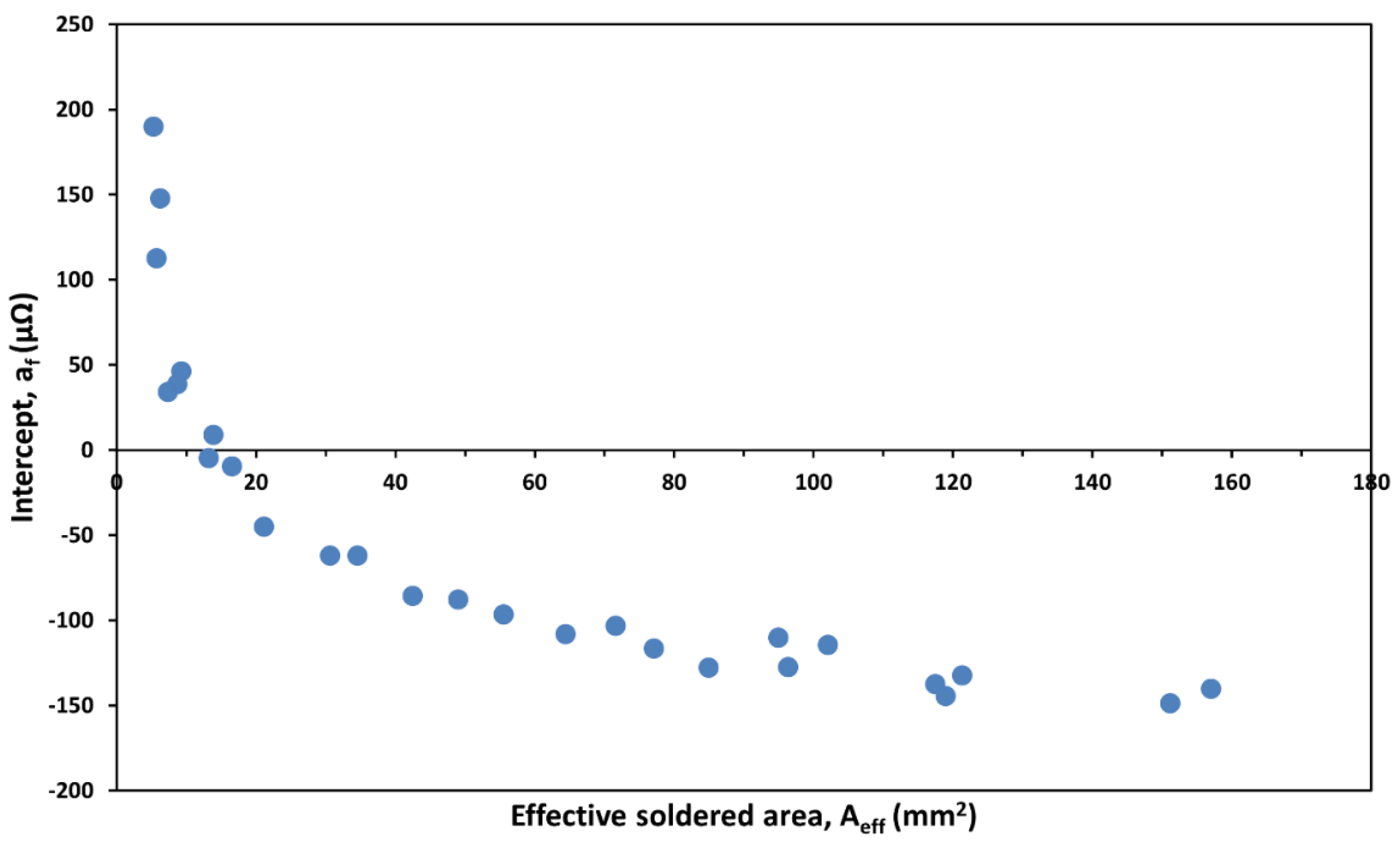
Figure 10.
The effect of changing the five relevant properties of the soldered joint by ± 50% on the slope of the R(d) function in near zone.
Figure 10.
The effect of changing the five relevant properties of the soldered joint by ± 50% on the slope of the R(d) function in near zone.
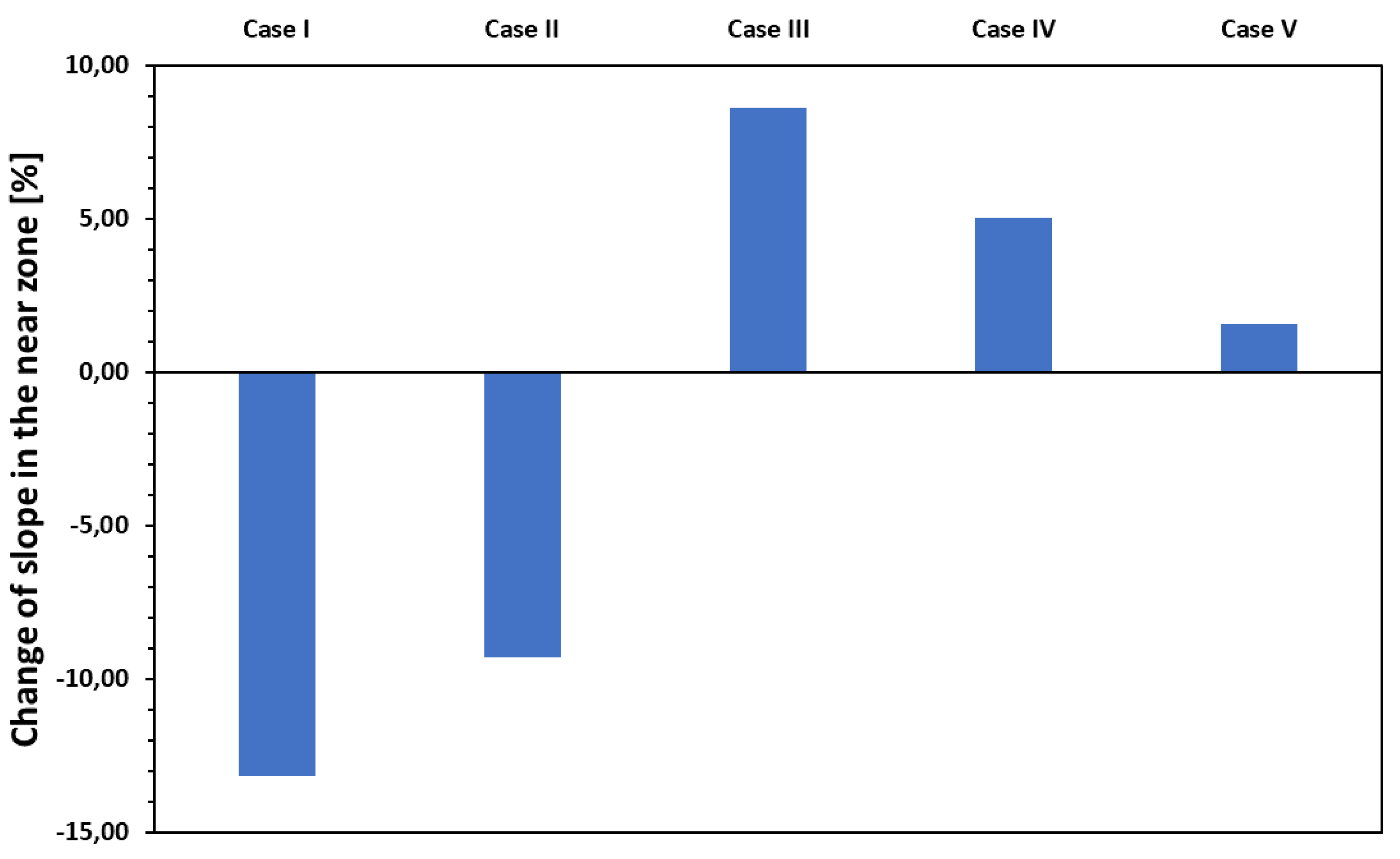
Figure 11.
Sketch of the joint indicating the quantities defining the c1 and c2 coefficients.
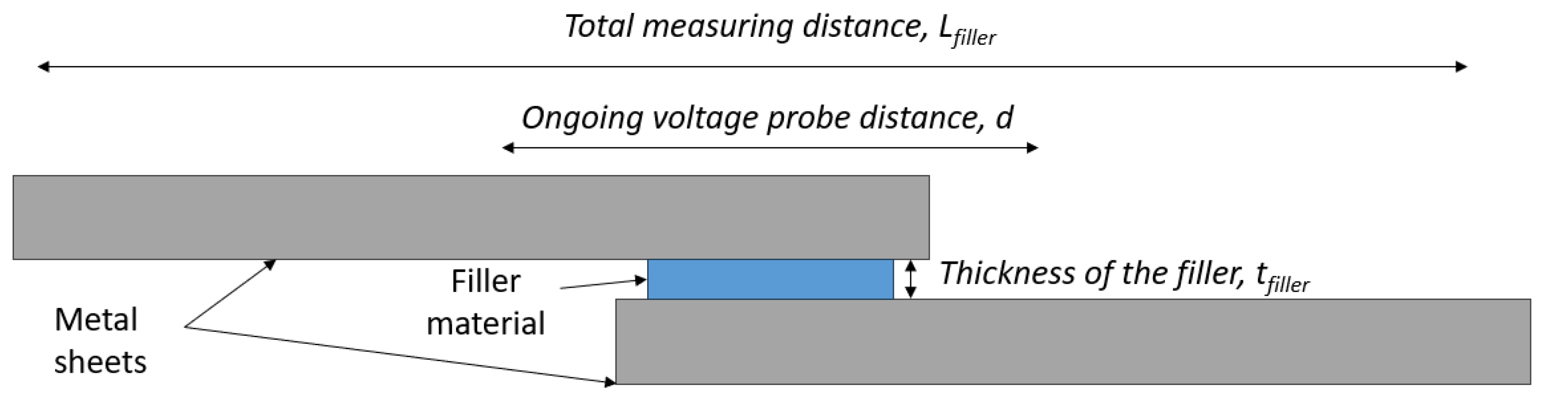
Figure 12.
The effect on the intercept in near zone of the five relevant properties of the soldered joint, when changing them ± 50% in relative terms to the measured data.
Figure 12.
The effect on the intercept in near zone of the five relevant properties of the soldered joint, when changing them ± 50% in relative terms to the measured data.
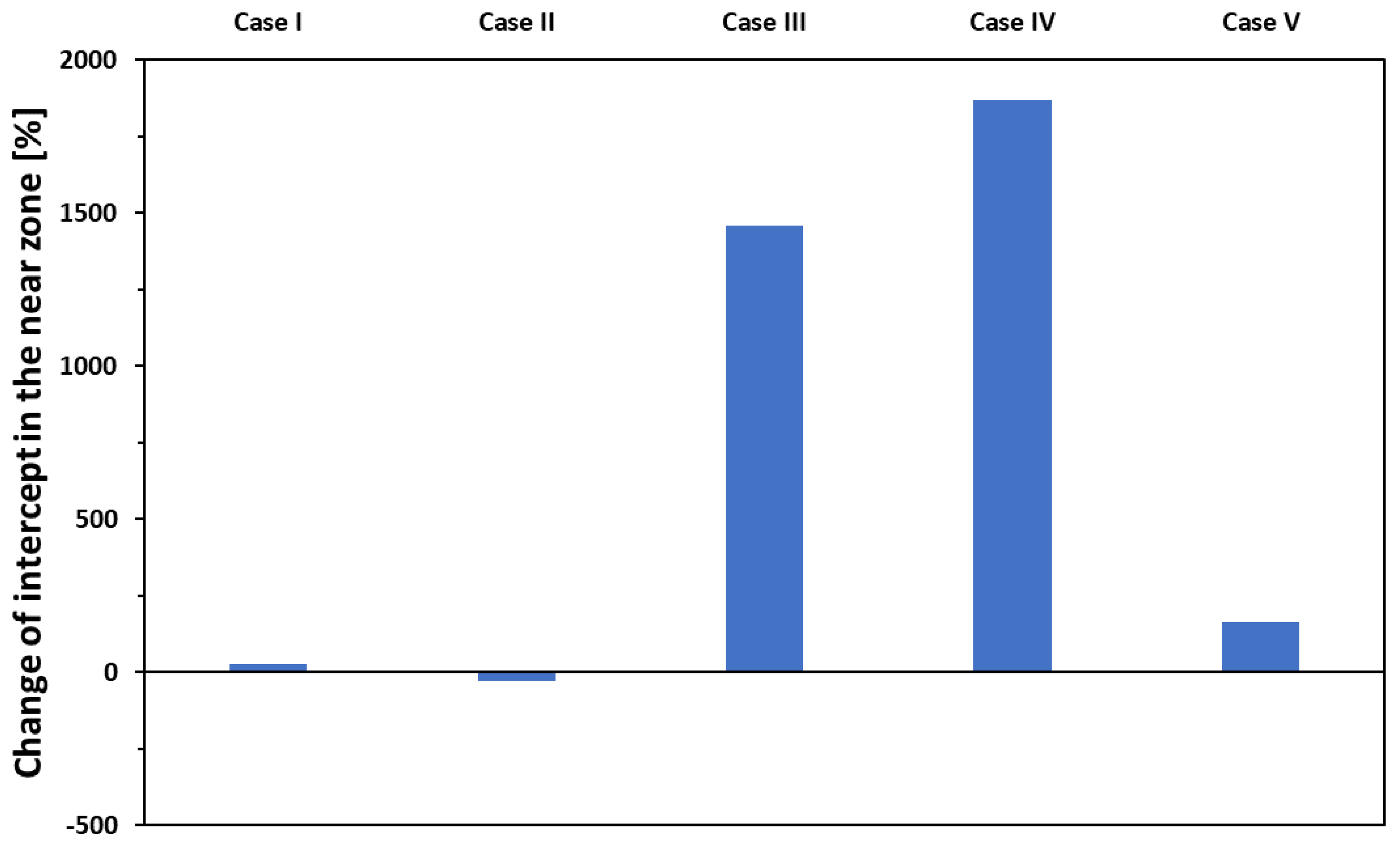
Figure 13.
a) The position of the joining area marked as red ring and the void. The appearance of the return current along the circumference of a void in filler material in 2D at z=0.53 mm section: b), and along x axis at y=7.5 mm: c).
Figure 13.
a) The position of the joining area marked as red ring and the void. The appearance of the return current along the circumference of a void in filler material in 2D at z=0.53 mm section: b), and along x axis at y=7.5 mm: c).
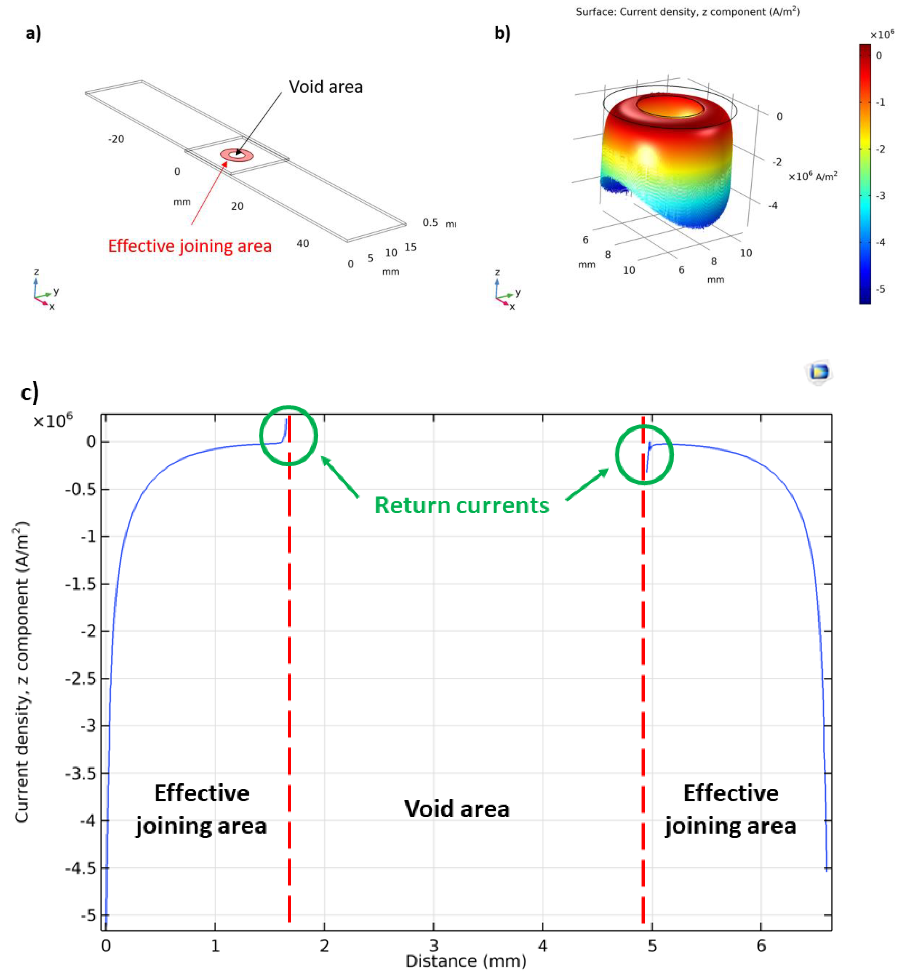

Table 1.
Measured values, and simulation ranges of the five varied properties describing the geometrical characteristics of a laser soldered sample (laser power of 120 W, irradiation time of 5 s, filler volume of 1.6 mm3).
Table 1.
Measured values, and simulation ranges of the five varied properties describing the geometrical characteristics of a laser soldered sample (laser power of 120 W, irradiation time of 5 s, filler volume of 1.6 mm3).
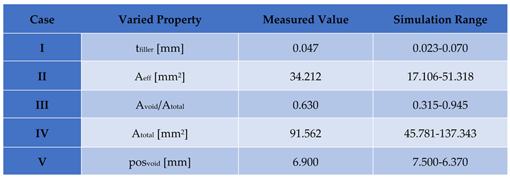
Table 2.
The slope of the R(d) curves in the far zone for different metal sheets.
Disclaimer/Publisher’s Note: The statements, opinions and data contained in all publications are solely those of the individual author(s) and contributor(s) and not of MDPI and/or the editor(s). MDPI and/or the editor(s) disclaim responsibility for any injury to people or property resulting from any ideas, methods, instructions or products referred to in the content. |
© 2024 by the authors. Licensee MDPI, Basel, Switzerland. This article is an open access article distributed under the terms and conditions of the Creative Commons Attribution (CC BY) license (http://creativecommons.org/licenses/by/4.0/).
Copyright: This open access article is published under a Creative Commons CC BY 4.0 license, which permit the free download, distribution, and reuse, provided that the author and preprint are cited in any reuse.


