Submitted:
07 May 2024
Posted:
07 May 2024
You are already at the latest version
Abstract
Abstract: NFinFET transistors with fin channel length 90nm and a planar MOSFET transistor with channel length 180nm and 90nm are presented with characteristic curves at various gate biases. A finalized algorithm with kink effects is effectively responsible for addressing the field effect transistors. The algorithm includes the modified conventional current-voltage formula and a nonlinear heat-associated kink solution which is simplified as a Gaussian form. Three parameters in modified model includes kN (related with channel width, channel length, and gate oxide capacitor, and proportional to the mobility of carriers)Vth(Threshold Voltage), and (the inverse of Early Voltage). Those parameters are determined to minimize the discrepancies between the measured data and the fitting values, but leave kinks located at around (VGS-Vth), which are deliberately eliminated by the Gaussian form because of the agitation of thermal kink effects. The whole fitting is made to be as close as the as-measured IDS-VDS. In the mean time, those determined parameters are physically meaningful after the analysis has been done.
Keywords:
Keywords: FinFET
; .Early Voltage
; channel length and width
1. Introduction
Short channel effects result in unwanted noticeable leakage current, which is successfully suppressed through halo-implant or pocket implant on, e.g., planar MOSFET with 0.18μm or 90nm long channel, in which the gate caps on the top of the channel. Unfortunately, the implant process fails to effectively stop leakage current on, e.g., 20nm any longer. Instead, FinFET sustains the capability of suppression of outrageously leaky current by using a gate-over-90%-surrounding 3-D slim channel for down to 3nm process technique. GAAFET replaces the role of FinFET by gate-completely-surrounding the whole channel for 2nm process technique. For one thing, the suppression of leakage current is due to creating depletion region in thin epi-taxial silicon which blocks the leakage current by building up a hill high potential barrier. However, the trend of shorter channels promotes the speed of transmitting signals via carriers and makes artificial intelligence (AI) possible, where the non-linear problem-sorting deep neural network (DNN), image-sorting convolution neural network (CNN), and speech-recognizing recurrent neural network (RNN) become available. [1,2,3,4,5,6]
Epi-silicon is tremendously important for its nearly identically flawless pure silicon that allows no enhancement of leakage current. Thicker epi-silicon film, such as tens of μm or a hundred μm, even plays roles of power discrete with high sustainable voltage bias. Thinner epi-silicon, such as 10 μm, is expected on integrated circuit (IC), though. Looking like an emerging 3-D “I” with two ends of Source and Drain, FinFET uses Gate poly-silicon crossing over the channel to conduct current in between Source and Drain by applying a bias to the Gate. Simultaneously, the Gate bias depletes the whole slim channel and builds up a barrier that blocks the leakage current. The achievable function of the process is mostly due to the good conformality (step coverage) of chemical vapor deposition, in which SiH4 (silane) is controlled at a chosen flow rate and the ambient is sustained at an appropriate temperature and at certain pressure to achieve a good deposition rate in kinetic regime.[7,8,9,10,11,12,13,14,15]
Somehow, the electrical performances of transistors are mainly manifested in current-versus-voltage characteristic curves. Those curves are necessarily parameter-extracted in the model, which is useful to develop circuit design. Therefore, the as measured I-V curves are thought to be well fitted to determine predominant parameters. In this study, an advisable algorithm using the “modified” conventional I-V characteristic curve formula along with kink effects generates fitting data to minimize the deviations from the measured ones. Promising are the as determined parameters, such as the threshold voltage (Vth), lambda (λ), and kN which is mainly proportional to the mobility.
2. Preparation, Measurements Fitting Algorithm
2.1. Preparation and Measurement of NFinFET
The grown 10μm epi-silicon layer is ionic dry etched to form a 3-dimensional 120nm wide and corresponding 9 times high fin channel. With two ends as Source and Drain, the whole epi-silicon channel looks like a letter “I”, which is followed with a grown thin gate oxide. The slim channel of “I” is then covered with arsenic heavily doped poly-silicon, called Gate. As the Gate is applied with a positive bias, the channel surrounded with Gate is then almost completely depleted, and right underneath the gate oxide, about 200 angstroms [16] p-type silicon gets strongly inversed into effectively 90nm long n-type silicon. The IDS versus VDS is then measured at various Gate biases.
2.2. Fitting IDS-VDS and IDS-VGS
The two-regime conventional formulas for FinFET and MOSFET transistors have to be modified as followed:
and
where VA is Early voltage, Cox(1) is gate oxide capacitance per square meter, Lo is channel length, μ is the mobility of carriers, and Weff=19Wo (Wo, fin width), and where β (V-1) is the kink width adjustment. [16,17,18,19,20,21]
Equation (1) or Equation (2) work as VDS is less than or larger than (VGS- Vth), respecitvely. And those parameters, (kN, Vth, λ, α, β, χ), are deliberately determined to minimize the delta (δ) as follows in Equation (3):
2.3. Fitting Algoritm
First, the minimum delta (δ) in Equation (3) may be used to first determine lambda (λ) by adjusting kN and Vth, leaving the locations of kinks at around VDS=(VGS–Vth). Then the discrepancies between the measured data and the fitting data are found to determine (χ, α) in Equation (1) and (2). Finally, the width of the kink (associated with β) at different VGS is to be determined by, again, the Equation (3). Totally, six parameters are used for the algorithm to well enough fit the characteristic curves. [21]
3. Results
There are three kinds of transistors, namely, FinFET W120L90 (Fin width =120nm, channel length=90nm), MOSFET L180nm (channel length =180nm), and MOSFET L90nm (channel length =90nm). According to the algorithm as described in 2.3, the measured data is fitted with conventional model formula with a little modification like Equation (1) and (2). The determined parameters are listed in Table 1, Table 2, and Table 3 as follows:
As shown in Figure 1 for FinFET, Figure 2 for MOSFET L180, and Figure 3 for MOSFET L090, the fitting without kink (heat or phonon effects) adjustment is presented in (a), where the lambda (λ), kN, and Vth are found. The differences between the as measured data and the fitting data are thus found in (b). In Figure 1b (double Gate side effects), the mono-peaks are set to where kinks are located and the twin-peaks are set to the shallow valleys in between where kinks are located. In Figure 2b and Figure 3b, there only found are the mono-peaks, where kinks are located. By means of the peaks, the parameters, (χ, α), are thus determined. The beta (β) is varied to find the minimum standard deviation resulting to the (c), (d), and (e). Actually, carriers receive thermal agitations from the kinks, which cause lower current flow.
4. Analysis and Discussion
The three main parameters listed in the Tables are associated with certain physical meanings. It is interesting to see the linearly dependent association as shown in Figure 4 such that kink and (VGS–Vth) are strongly correlated and linearly dependent to each other as well. This demonstrates and enhances the ideas of the kink effects addressing the phonon disturbances on, scattering from, and coupling with the carriers degrading the electrical performances.
Furthermore, kN with geometrical fixed sizes is proportional to mobility (μ), which is demonstrated as a constant value at fixed VGS. But at different applied VGS bias, mobility is definitely various and proportional to (VGS-Vth)-1/3, as shown in Figure 5a, 5b and 5c. In Figure 5b, VGS=0.8V shall be excluded from the proportionality because less strong inversion layer does not result in effective oxide-silicon interfacial colliding carriers. Moreover, the threshold voltages (Vth) vary at various VGS not only for FinFET but also for MOSFET, where Vtho may be written as follows:
where “FB” means flat-band voltage, Qox is the charge located in the oxide layer, Cox’ is the unit capacitance, Qdep is the space charge in the depletion region, and 2|Φ| is the basic applied VGS that causes the strongly inversed layer for Vtho. Somehow, the Equation (3) is rewritten as the following fitting formula:
In Equation (4), f(VGS)=(1–VGS) is defined to deliberately set the condition of VGS under 1.0 V.[22] In the fitting presented in Figure 6a and 6b, |β|=0.085 and |β|=0.1 correspond to p=4.4×10²³ (1/m3) and p=1.6163×10²² (1/m3), which help identify the thickness of strongly inversed layer to be 182 angstrom at VGS_FinFET=1.0V and 92 angstrom at VGS_MOSFET=0.4V, as referred in Figure 6c.
In addition, λ(|VA-1|) signifies the leakage current slope across Source and Drain and shows suppressed as (VGS–Vth) increases, which means more depletion region induces leakage current reduction, as in Figure 7(a), 7(b), and 7(c).
5. Conclusions
The modified characteristic formulas in Equation (1) and (2) with kink effects (phonon disturbances) provide to fit the as-measured current-voltage curves. The kinks always locate at the joint of Triode region and Saturation region. The standard deviation helps make the fitting as completely as possible such that three parameters (kN, Vth, λ) are determined. The mobility at certain fixed Gate voltage, which is proportional to kN, is constant but various at various Gate bias. For FinFET and MOSFET, kN is found to be almost linearly dependent of (VGS-Vth)-1/3, and so is mobility. The determined Vth is found to be VGS-dependent, too. The empirical equation, which takes advantage of the definition of Vtho, is proposed in order to find β and thus the concentration (p) of doped boron, which may be used to calculate the thickness of the strong inversion layer. In addition, Early Voltage associated λ (|VA-1|), which is inversely linearly dependent of (VGS–Vth), gets flatter as (VGS–Vth) gets larger. This indicates that higher field more depleting the substrate depresses the leakage current.
Author Contributions
Conceptualization, H.C. Yang., and S.C. Chi.; methodology, H.C. Yang, S.C. Chi, H.Y Yang, and Y.T. Yang; software, H.C. Yang., and S.C. Chi; validation, H.C. Yang., and S.C. Chi; formal analysis, H.C. Yang., and S.C. Chi.; investigation, H.C. Yang., and S.C. Chi; resources, H.C. Yang., and S.C. Chi; data duration, H.C. Yang., and S.C. Chi.
Funding
Not available.
Institutional Review Board Statement
Not available.
Informed Consent Statement
Not available.
Data Availability Statement
No.
Conflicts of Interest
No.
Appendix A
Reviewer 1: Author's Reply to the Review Report (Reviewer 1).
| Yes | Can be improved | Must be improved | Not applicable | |
| Does the introduction provide sufficient background and include all relevant references? | ( ) | ( ) | (x) | ( ) |
| Are all the cited references relevant to the research? | ( ) | ( ) | (x) | ( ) |
| Is the research design appropriate? | ( ) | ( ) | (x) | ( ) |
| Are the methods adequately described? | ( ) | ( ) | (x) | ( ) |
| Are the results clearly presented? | ( ) | ( ) | (x) | ( ) |
| Are the conclusions supported by the results? | ( ) | ( ) | (x) | ( ) |
Comments and Suggestions for Authors
(1) The paper on "Conclusive Algorithm with Kink Effects for Fitting 3-D FinFET and Planar MOSFET Characteristic Curves" is very poor quality. It is just a pure fitting exercize and does not bring any practical or physical insight into the MOSFET operation.
Answer to (1):Thank you for the authentic criticizing. There comes another exercising added for trying to realizing the model.
(2) The model used is essentially the same as the one published by the same authors in refs 16-21.
Answer to (2): In order to realize if the model is applicable, the cases are re-examined.
(3) Moreover, the fitting analysis is made on only one gate length, which is not sufficient to bring any conclusion for short vs long channel and say something true about the operation of devices.
Answer to (3): We would rather understand the electrical performances step by step.
Are the devices used really existing and real? ( It is for sure existing and real.)
(4) The term kink effects is misleading as generally refering to substrate debiasing due floating body effects. Here it seems this refers to phonon related effect badly explained even in ref 21.
Answer to (4): Floating body effects mainly refer to SOI, but FBE are also found in transistors without SOI applications here for the planar MOSFET, Therefore, there added is the case study about MOSFET L090. On the other hand, the equivalent capacitance is supposed to be small, and kink effects are also termed in another applications such as nonlinear Quantum Field Theory..
(5) Moreover the model is quite simplistic as there is no mobility effects neither saturation velocity effects in this model. Also the model is essentially limited to strong inversion (above Vth) and is not interesting as a compact model for circuit simlation as not containing the subthreshold region.
Answer to (5): The saturation mechanism is as follows (which is discussed somewhere else)
Furthermore, current flows because of flowing carriers, moving electrons or holes, which carry electrical power or signals. Somehow, the current, IC, eventually gets saturated and reaches a certain quantity since the carriers can not be accelerated any more and stay at a maximum speed. The electrical force accelerates carriers and cancels with the frictional force, which is proportional to the Nth power of the speed and opposite to the moving direction of carriers. For simplicity, only electrons are taken into account and the total force F is characterized as follows:
 where α is a viscosity coefficient, m is the mass of carriers, and E is the electrical force coming from the applied bias across the channel. Before electrons reach the maximum speed,
 where l is the traverse distance length that the electron travels as E is applied. So,
 where
where
From Equation (7), the traverse distance l may approach to infinity as the speed approaches to certain value at certain applied electrical field ED =VDS/L as stated below:
 and
and
 which gives the information that the mobility in the conventional ID(VD, VG) formula in Equation (2) is constant only when N=1 at certain fixed gate bios.
The scale of electrical data addressing performances at sub-threshold voltage is quite small and skeptical because the measurement tool at the scale, e.g., peco-Amp or even a little higher, is not precise enough. In addition, this range of electronic performances can never be applied to any applications.
(6) A complete MOSFET parameter extraction should be done by first looking at linear region for various Vg and varous gate length. Then the Vd bias influence should be studied.
Answer to (6): Ids-Vds and Ids-Vgs share the same formulas and the same data, which means both curves are identically transformable to each other once the fitting is completed.
Submission Date
27 January 2024
Date of this review
05 Feb 2024 09:02:09
Reviewer 2: Author's Reply to the Review Report (Reviewer 2).
| Yes | Can be improved | Must be improved | Not applicable | |
| Does the introduction provide sufficient background and include all relevant references? | ( ) | ( ) | ( ) | (x) |
| Are all the cited references relevant to the research? | ( ) | ( ) | (x) | ( ) |
| Is the research design appropriate? | ( ) | ( ) | ( ) | (x) |
| Are the methods adequately described? | ( ) | ( ) | ( ) | (x) |
| Are the results clearly presented? | ( ) | ( ) | (x) | ( ) |
| Are the conclusions supported by the results? | ( ) | ( ) | (x) | ( ) |
Comments and Suggestions for Authors

The overall quality of this paper is seriously low.
(1)- 3nm technology does not use 3nm long channel.
Answer to (1): Thanks a lot. It has been changed to 3nm process technology, which is associated with the width of the fin.
(2)- Insufficient information about the measured NFinFET.
Answer to (2) Please refer to Yang, H.-C., Jui-Ming Tsai, Tsin-Yuan Chang, Wen-Shiang Liao, Sung-Ching Chi; The Effects of Thickness of Source/Drain Fin on P-Channel FinFET Devices and the Corresponding Quantum Effects, p165-169, Nano-science Nanotechnology Lett. 2014, Vol 6, No 2, which talked about NFinFET process details..
(3)- 120nm width fin cannot be operate as typical FinFET. It may not have enough double-gate effect.
Answer to (3): Please refer to Yang, H.-C., Jui-Ming Tsai, Tsin-Yuan Chang, Wen-Shiang Liao, Sung-Ching Chi; The Effects of Thickness of Source/Drain Fin on P-Channel FinFET Devices and the Corresponding Quantum Effects, p165-169, Nano-science Nanotechnology Lett. 2014, Vol 6, No 2, which talked about double gate effect.
(4)- All the fitting process has no meaningful results and no significance.
Answer to (4) Thanks a lot.
- Graphic quality is too low.
Answer to (4) Thanks a lot
Submission Date
27 January 2024
Date of this review
20 Feb 2024 14:53:16
References
- Diab, A.; Torres Sevilla, G.-A.; Christoloveanu, S.; and Hussain, M.-M. Room to high temperature measurements of flexible SOI FinFETs with sub-20-nm fins. IEEE Trans. Electron. Devices 2014, 61, 3978. [Google Scholar] [CrossRef]
- Wang, F.; Xie, Y.; Bernstein, K.; Luo, Y. Dependability analysis of nano-scale FinFET circuits. In Proceedings of the IEEE Computer Society Annual Symposium on Emerging VLSI Technologies and Architectures (ISVLSI'06), Karlsruhe, Germany, 2–3 March 2006; pp 6, 399.
- Huang, X.; Lee, W.-C.; Kuo, C.; Hisamoto, D.; Chang, L.; Kedzierski, J.; Anderson, E.; Takeuchi, H.; Choi, Y.-K.; Asano, K.; et al. Sub-50 nm P-channel FinFET. IEEE Trans. Electron. Devices 2001, 48, 880. [Google Scholar] [CrossRef]
- Rudenko, T. , Kilchytska, V., Arshad, M.K.M., Raskin, J.-P., Nazarov, A. and Flandre, D. On the MOSFET Threshold Voltage Extraction by Transconductance and Transconductance-to-Current Ratio Change Methods: Part II-Effect of Drain Voltage. IEEE Trans. Electron. Devices, 2011; 58, 4180–4188. [Google Scholar]
- Takahashi, T.; Beppu, N.; Chen, K.; Oda, S.; Uchida, K. Self-heating effects and analog performance optimization of Fin-type field-effect transistors. Jpn. J. Appl. Phys. 2013, 52, 04CC03. [Google Scholar] [CrossRef]
- Saitoh, M.; Yasutake, N.; Nakabayashi, Y.; Uchida, K.; Numata, T. Understanding of strain effects on high-field carrier velocity in (100) and (110) CMOSFETs under quasi-ballistic transport. 2009 IEEE International Electron Devices Meeting (IEDM), Baltimore, MD, USA, 07-09 December; pp. 1-4.
- Chen, C.W.; Wang, S.J.; Hsieh, W.C.; Chen, J.M.; Jong, T.; Lan, W.H.; Wang, M.C. Q-factor Performance of 28 nm-node High-k Gate Dielectric under DPN Treatment at Different Annealing Temperatures. Electronics 2020, 9, 2086. [Google Scholar] [CrossRef]
- Lu, P.; Yang, C.; Li, Y.; Li, B.; Han, Z. Three-Dimensional TID Hardening Design for 14 nm Node SOI FinFETs. Eng 2021, 2, 620–631. [Google Scholar] [CrossRef]
- Song, Y.S.; Tayal, S.; Rahi, S.B.; Kim, J.H.; Upadhyay, A.K.; Park, B.-G. Thermal-Aware IC Chip Design by Combining High Thermal Conductivity Materials and GAA MOSFET. In Proceedings of the 2022 5th International Conference on Circuits, Systems and Simulation (ICCSS), Nanjing, China, 13-15 May 2022; pp. 135–140. [Google Scholar]
- Crupi, G.; Schreurs, D.M.M.-P.; Caddemi, A.; Angelov, I.; Homayouni, M.; Raffo, A.; Vannini, G.; Parvais, B. Purely analytical extraction of an improved nonlinear FinFET model including non-quasi-static effects. Microelectron. Eng. 2009, 86, 2283–2289. [Google Scholar] [CrossRef]
- Li, Y.; Zhao, F.; Cheng, X.; Liu, H.; Zan, Y.; Li, J.; Zhang, Q.; Wu, Z.; Luo, J.; Wang, W. Four-Period Vertically Stacked SiGe/Si Channel FinFET Fabrication and Its Electrical Characteristics. Nanomaterials 2021, 11, 1689. [Google Scholar] [CrossRef] [PubMed]
- Zhao, E.; Zhang, J.; Salman, A.; Subba, N.; Chan, J.; Marathe, A.; Beebe, S.; Taylor, K. Reliability challenges of high performance PD SOI CMOS with ultra-thin gate dielectrics. Solid State Electron. 2004, 48, 1703–1708. [Google Scholar] [CrossRef]
- Zhao, Z.Q.; Li, Y.; Zan, Y.; Li, Y.L.; Li, J.J.; Cheng, X.H.; Wang, G.L.; Liu, H.Y.; Wang, H.X.; Zhang, Q.Z.; et al. Fabrication technique of the Si0.5Ge0.5 Fin for the high mobility channel FinFET device. Semicond. Sci. Technol. 2020, 35, 045015. [Google Scholar] [CrossRef]
- Lee, J.; Park, T.; Ahn, H.; Kwak, J.; Moon, T.; Shin, C. Prediction Model for Random Variation in FinFET Induced by Line-Edge-Roughness (LER). Electronics 2021, 10, 455. [Google Scholar] [CrossRef]
- B. Van Zeghbroeck, Priciples of Semiconductor Devices, Chapter 7.6 Advanced MOSFET issues. http: //ece-www. colorado. edu/~bart/ book/book/title.htm [2/28/2002 5:26:12 PM].
- Yang, H.-C.; Chi, S.-C. Process Corresponding Implications Associated with a Conclusive Model-Fit Current-Voltage Characteristic Curves. Appl. Sci. 2022, 12, 462. [Google Scholar] [CrossRef]
- Yang, H.-C.; Chi, S.-C.; Liao, W.S. Comparison of Fitting Current–Voltage Characteristics Curves of FinFET Transistors with Various Fixed Parameter. Appl. Sci. 2022, 12, 10519. [Google Scholar] [CrossRef]
- Ryder, L. H. The sine-Gordon kink, In Quantum Field Theory, the Press Syndicate of the University of Cambridge, Cambridge , UK, 1985, pp402.
- D. Lacroix, I. Traore, S. Fumwron, and G. Jeandel. Phonon transport in silicon, influence of the dispersion properties choice on the description of the anharmonics resistive mechanisms. Eur. Phys. J. B 2009, 67, 15–25.
- Kang, S.-M.; Leblebici, Y. CMOS Digital Integrated Circuits: analysis and design, Chapter 4 Modeling of MOS Transistors Using SPICE, p111, Published by McGRAW-Hill International Editions, ISBN 0-07-114423-4.
- Yang, H.-C.; Chi, S.-C. Conclusive Model-Fit Current Voltage Characteristic Curves with Kink Effects. Appl. Sci. 2023, 13, 12379. [Google Scholar] [CrossRef]
- Yang, H.-C. , Jui-Ming Tsai, Tsin-Yuan Chang, Wen-Shiang Liao, Sung-Ching Chi; The Effects of Thickness of Source/Drain Fin on P-Channel FinFET Devices and the Corresponding Quantum Effects, p165-169, Nano-science Nanotechnology Lett. 2014, Vol 6, No 2.
Figure 1.
(a) FinFET fitting without considering thermal phonon collisions. (b) δ=7.63×10⁻⁷ Amp (at VGS=1.0V), δ=6.89×10⁻⁷ Amp (at VGS=0.75V), δ=5.33×10⁻⁷ Amp (at VGS=0.5V), and δ=2.29×10⁻⁷ Amp (at VGS=0.25V) (c) FinFET fitting with considering thermal phonons collision. (d) Minimum standard deviation: δ=1.23×10⁻⁷ Amp (at VGS=1.0V), δ=1.19×10⁻⁷ Amp (at VGS= 0.75V), δ=9.26×10⁻⁸ Amp (at VGS=0.5V), and δ=3.46×10⁻⁸ Amp (at VGS=0.25V) (e) Minimum standard deviation: δ=1.23×10⁻⁷ Amp (at VGS=1.0V).
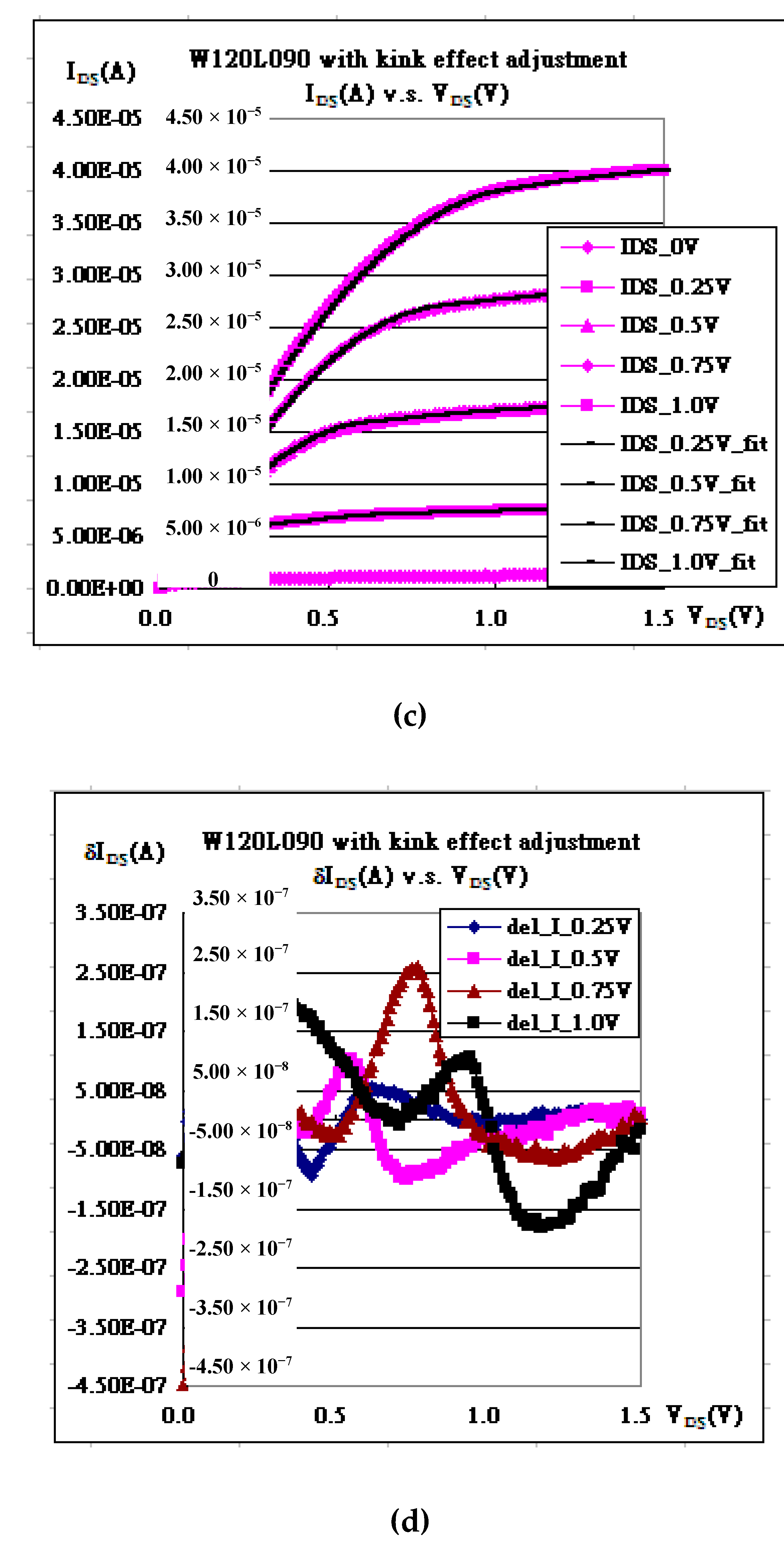
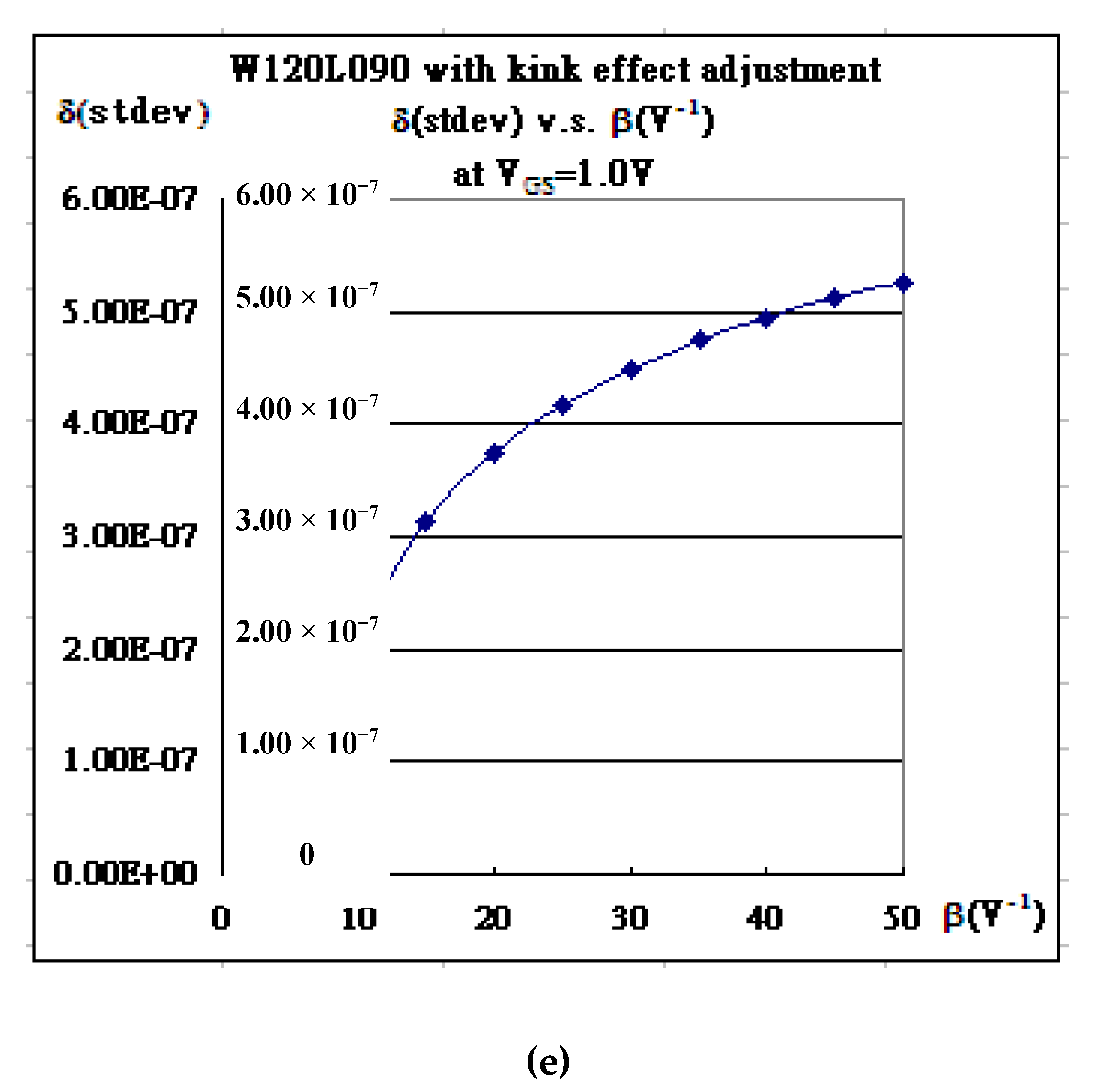
Figure 2.
(a) L180-MOSFET fitting without considering thermal phonon collisions. (b) δ=1.92×10⁻³ Amp (at VGS=2.5V), δ=1.27×10⁻³ Amp (at VGS=2.2V), δ=1.24×10⁻³ Amp (at VGS=2.0V), and δ=9.40×10⁻⁴ Amp (at VGS=1.8V), δ=8.56×10⁻⁴ Amp (at VGS=1.5V), δ=6.09×10⁻⁴ Amp (at VGS=1.2V), δ=4.08×10⁻⁴ Amp (at VGS=1.0V), and δ=2.27×10⁻⁴ Amp (at VGS=0.8V) (c) L180-MOSFET fitting with considering thermal phonons collision. (d) Minimum standard deviation: δ=3.03×10⁻⁴ Amp (at VGS=2.5V), δ=2.00×10⁻⁴ Amp (at VGS=2.2V), δ=2.77×10⁻⁴ Amp (at VGS=2.0V), δ=1.91×10⁻⁴ Amp (at VGS=1.8V), δ=1.46×10⁻³ Amp (at VGS=1.5V), δ=1.40×10⁻⁴ Amp (at VGS=1.2V), δ=7.82×10⁻⁵ Amp (at VGS=1.0V), and δ=6.81×10⁻⁵ Amp (at VGS=0.8V) (e) Minimum standard deviation: δ=3.03×10⁻⁴ Amp (at VGS=2.5V).
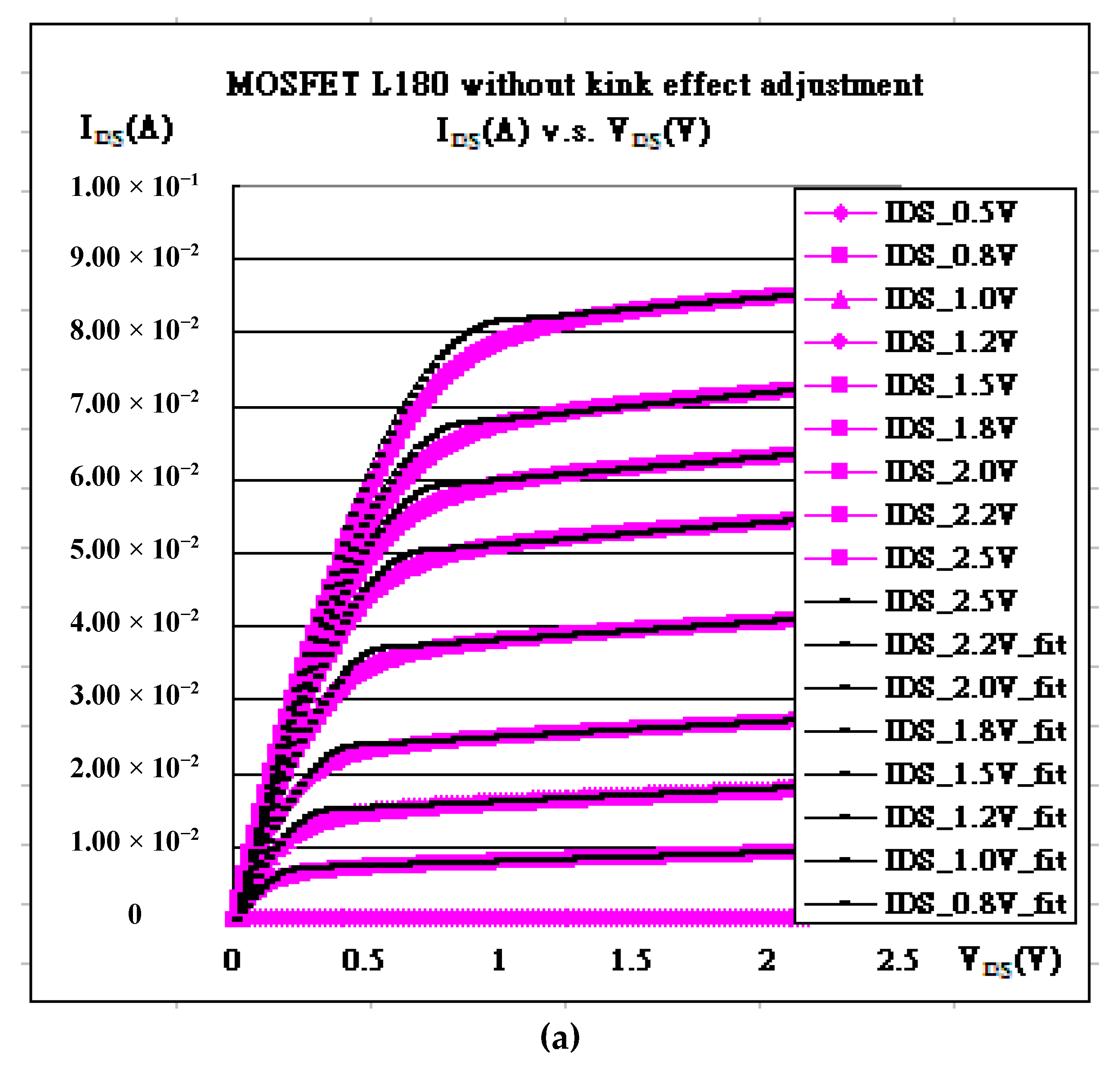
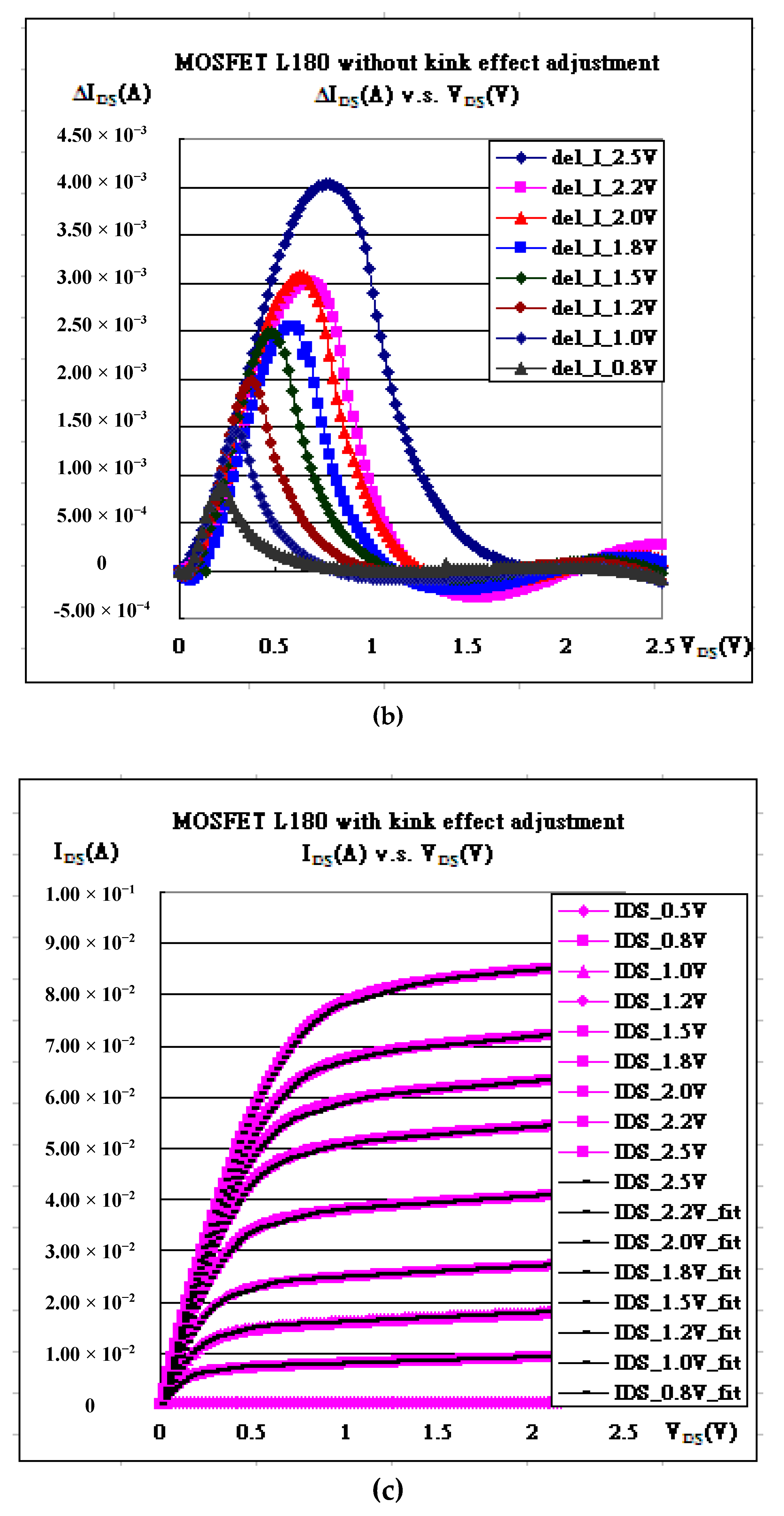
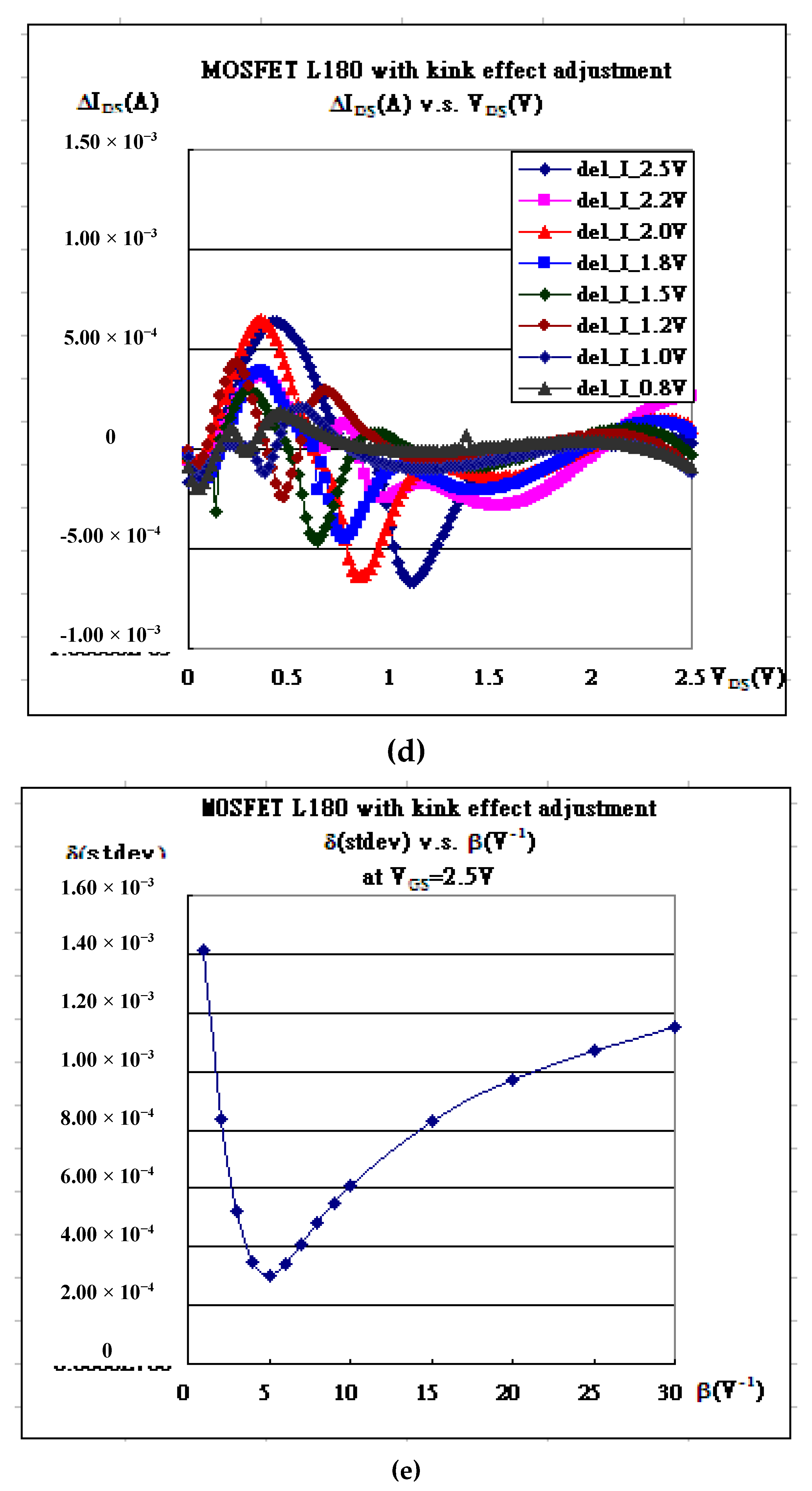
Figure 3.
(a) L90-MOSFET fitting without considering thermal phonon collisions. (b) δ=7.35×10⁻⁶ Amp (at VGS=2.2V), δ=5.05×10⁻⁶ Amp (at VGS=2.0V), δ=3.29×10⁻⁶ Amp (at VGS=1.8V), δ=2.15×10⁻⁶ Amp (at VGS=1.5V), δ=1.35×10⁻⁶ Amp (at VGS=1.2V), δ=1.02×10⁻⁶ Amp (at VGS=1.0V), and δ=6.97×10⁻⁷ Amp (at VGS=0.8V) (c) L90-MOSFET fitting with considering thermal phonons collision. (d) Minimum standard deviation: δ=1.35×10⁻⁶ Amp (at VGS=2.2V), δ=1.29×10⁻⁶ Amp (VGS=2.0V), δ=1.15×10⁻⁶ Amp (at VGS=1.8V), δ=3.17×10⁻⁷ Amp (at VGS=1.5V), δ=2.17×10⁻⁷ Amp (at VGS=1.2V), δ=1.61×10⁻⁷ Amp (at VGS=1.0V), and δ=1.68×10⁻⁷ Amp (at VGS=0.8V) (e) Minimum standard deviation: δ=1.35×10⁻⁶ Amp (VGS=2.2V).
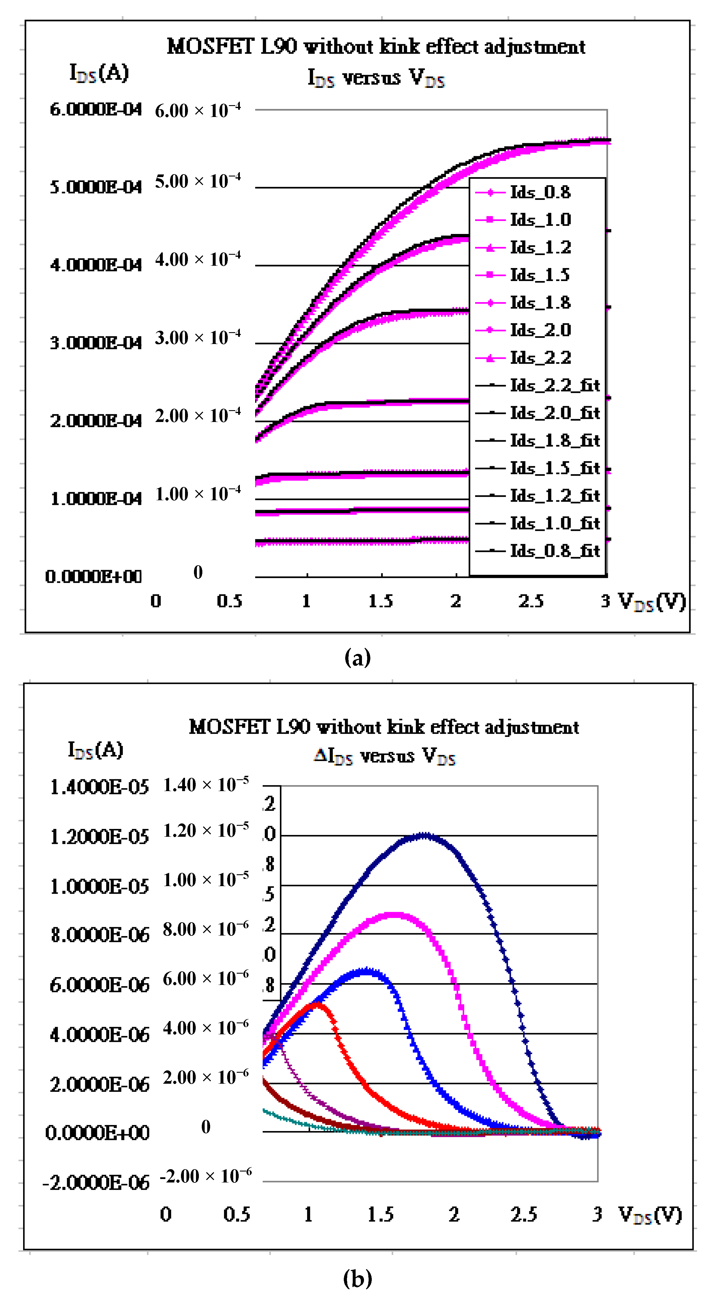
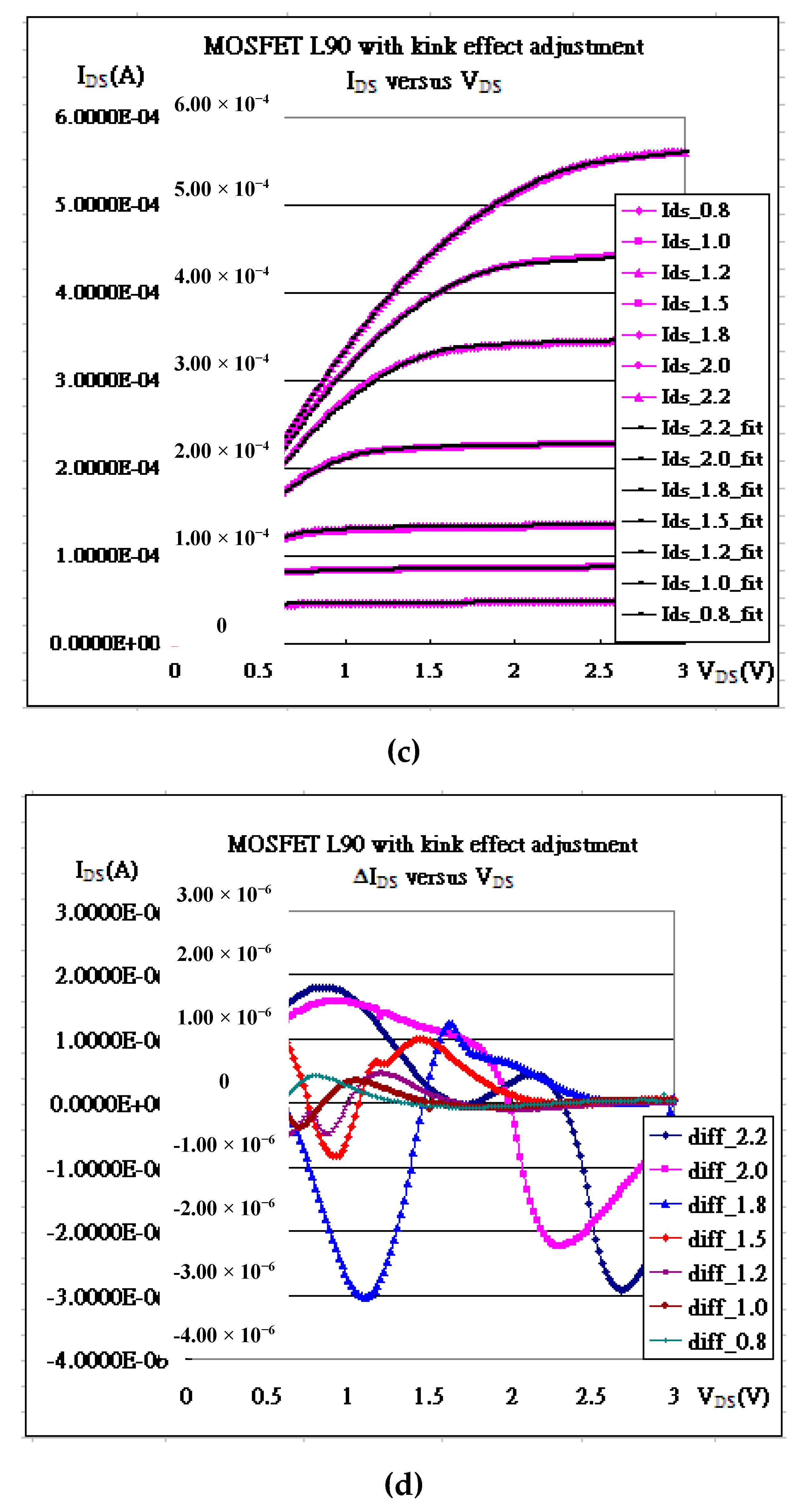
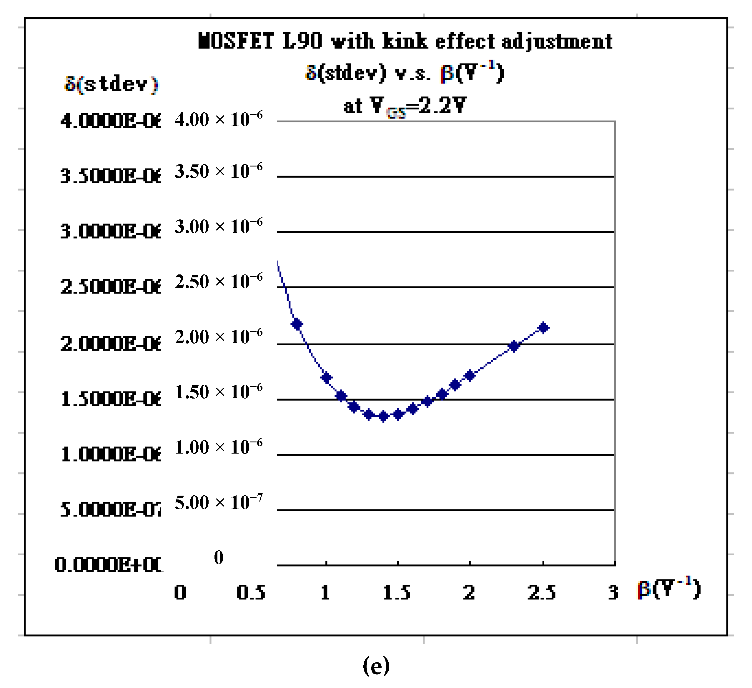
Figure 4.
(VGS–Vth) versus VGS, and versus VGS. (a) FinFET W120L90, (b) MOSFET L180, (c) MOS FET L090.
Figure 4.
(VGS–Vth) versus VGS, and versus VGS. (a) FinFET W120L90, (b) MOSFET L180, (c) MOS FET L090.
Figure 5.
(a) kN is proportional to (VGS-Vth)-1/3 for FinFET, (b) kN is proportional to (VGS-Vth)-1/3 for L-180 MOSFET, (c) kN is approximately proportional to (VGS-Vth)-1/3 for L-90 MOSFET.
Figure 5.
(a) kN is proportional to (VGS-Vth)-1/3 for FinFET, (b) kN is proportional to (VGS-Vth)-1/3 for L-180 MOSFET, (c) kN is approximately proportional to (VGS-Vth)-1/3 for L-90 MOSFET.
Figure 6.
(a) Vth versus VGS for FinFET, (b) Vth versus VGS for FinFET, (c)Depletion region and strongly inversed layer in energy region presentation.
Figure 6.
(a) Vth versus VGS for FinFET, (b) Vth versus VGS for FinFET, (c)Depletion region and strongly inversed layer in energy region presentation.
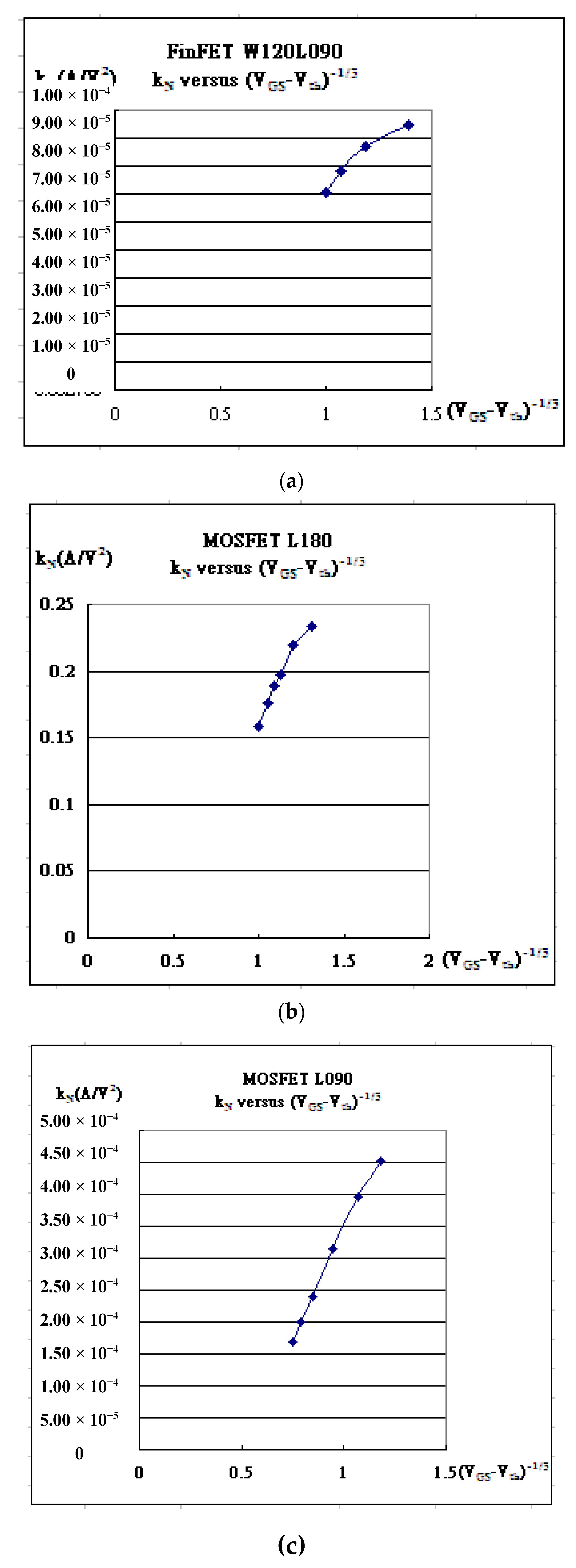
Figure 7.
(a) λ versus (VGS–Vth)-1for FinFET, (b) λ versus (VGS–Vth)-1 for L180 MOSFET (b) λ versus (VGS–Vth)-1 for L90 MOSFET.
Figure 7.
(a) λ versus (VGS–Vth)-1for FinFET, (b) λ versus (VGS–Vth)-1 for L180 MOSFET (b) λ versus (VGS–Vth)-1 for L90 MOSFET.
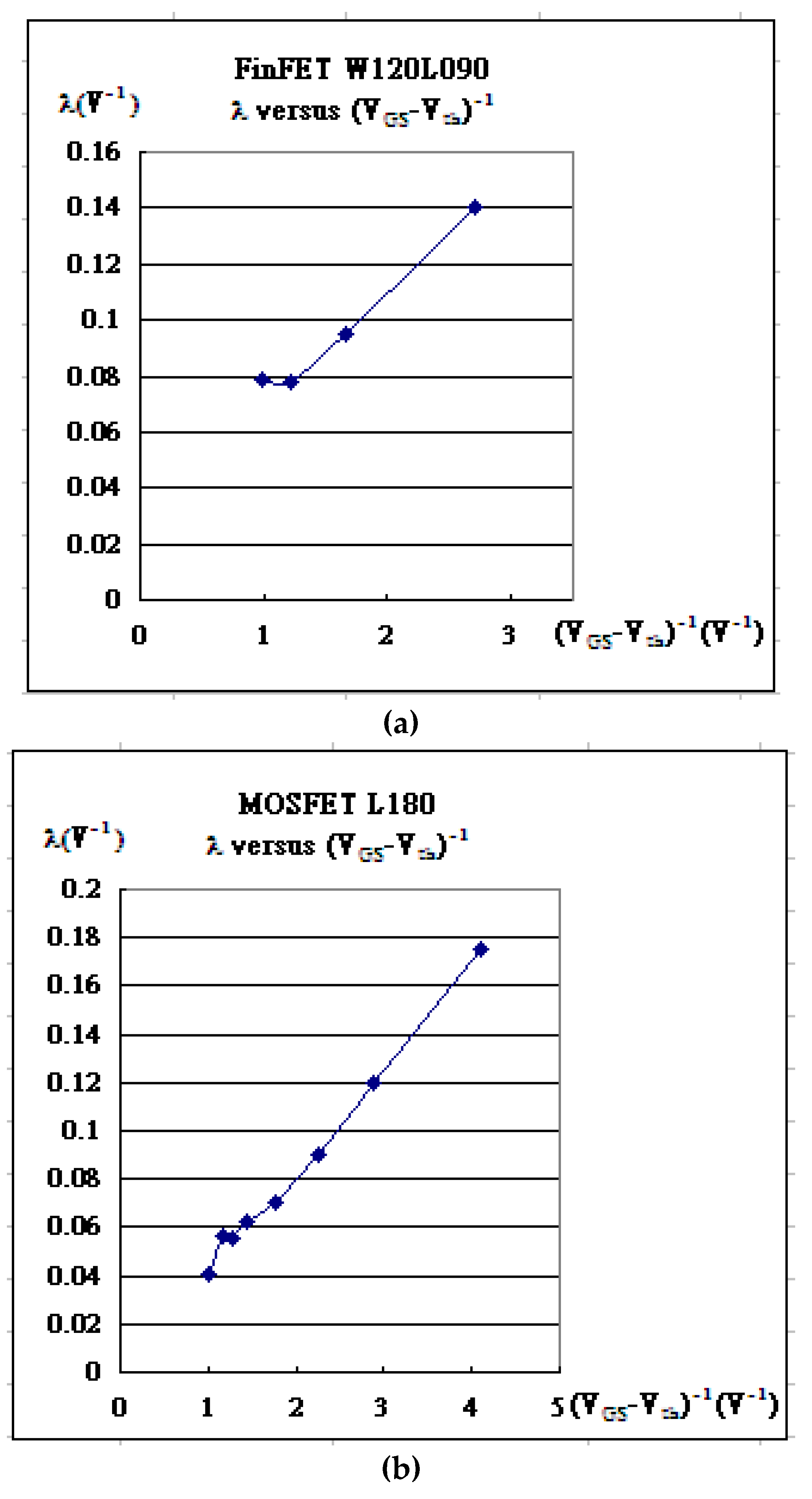

Table 1.
Determined parameters of FinFET W120L90 ( Fin Width=120nm, Length=90nm).
| Gate Bias | kN | Vth | λ | Kink (χ) | α |
|---|---|---|---|---|---|
| VGS = 0.25V | 9.50×10⁻⁵ | -0.1197 | 0.140 | 0.33 | 5.95×10⁻⁷ |
| VGS = 0.50V | 8.73×10⁻⁵ | -0.0981 | 0.095 | 0.44 | 8.9×10⁻⁷ |
| VGS = 0.75V | 7.78×10⁻⁵ | -0.065 | 0.078 | 0.56 | 1.09×10⁻⁶ |
| VGS = 1.00V | 7.07×10⁻⁵ | -0.007 | 0.079 | 0.68 | 1.22×10⁻⁶ |
Table 2.
Determined parameters of MOSFET L180 ( Length=180nm).
| Gate Bias | kN | Vth | λ | Kink (χ) | α |
|---|---|---|---|---|---|
| VGS = 0.80V | 0.228 | 0.556 | 0.17 | 0.22 | 7.7781×10⁻⁴ |
| VGS = 1.00V | 0.24 | 0.654 | 0.12 | 0.3 | 1.4426×10⁻³ |
| VGS = 1.20V | 0.234 | 0.7585 | 0.09 | 0.38 | 1.9528×10⁻³ |
| VGS =1.50V | 0.22 | 0.931 | 0.07 | 0.48 | 2.4542×10⁻³ |
| VGS = 1.80 V | 0.197 | 1.101 | 0.062 | 0.6 | 2.5051×10⁻³ |
| VGS = 2.00V | 0.189 | 1.225 | 0.055 | 0.64 | 3.1098×10⁻³ |
| VGS = 2.20V | 0.1765 | 1.345 | 0.056 | 0.7 | 3.006×10⁻³ |
| VGS = 2.50 V | 0.155 | 1.505 | 0.051 | 0.8 | 4.016×10⁻³ |
Table 3.
Determined parameters of MOSFET L90 ( Length=90nm).
| Gate Bias | kN | Vth | λ | Kink (χ) | I_Kink (α) |
|---|---|---|---|---|---|
| VGS = 0.80V | 5.000×10⁻⁴ | 0.3772 | 0.028 | 0.40 | 2.3966×10⁻⁶ |
| VGS = 1.00V | 4.530×10⁻⁴ | 0.398 | 0.022 | 0.56 | 3.2207×10⁻⁶ |
| VGS = 1.20V | 3.950×10⁻⁴ | 0.3905 | 0.0184 | 0.74 | 3.8950×10⁻⁶ |
| VGS =1.50V | 3.150×10⁻⁴ | 0.3215 | 0.0155 | 1.04 | 5.1265×10⁻⁶ |
| VGS = 1.80 V | 2.400×10⁻⁴ | 0.1345 | 0.014 | 1.4 | 6.5264×10⁻⁶ |
| VGS = 2.00V | 2.000×10⁻⁴ | -0.063 | 0.0145 | 1.6 | 8.7565×10⁻⁶ |
| VGS = 2.20V | 1.680×10⁻⁴ | -0.17 | 0.027 | 1.78 | 1.1965×10⁻⁵ |
Disclaimer/Publisher’s Note: The statements, opinions and data contained in all publications are solely those of the individual author(s) and contributor(s) and not of MDPI and/or the editor(s). MDPI and/or the editor(s) disclaim responsibility for any injury to people or property resulting from any ideas, methods, instructions or products referred to in the content. |
© 2024 by the authors. Licensee MDPI, Basel, Switzerland. This article is an open access article distributed under the terms and conditions of the Creative Commons Attribution (CC BY) license (http://creativecommons.org/licenses/by/4.0/).
Copyright: This open access article is published under a Creative Commons CC BY 4.0 license, which permit the free download, distribution, and reuse, provided that the author and preprint are cited in any reuse.


