Submitted:
06 May 2024
Posted:
06 May 2024
You are already at the latest version
Abstract
In this work, an analog front-end (AFE) circuit for Electrocardiogram (ECG) detection system has been designed, implemented, and investigated in an industry-standard Cadence simulation framework using advanced technology node of 45 nm. The AFE consists of an instrumentation amplifier, a Butterworth band-pass filter (with fifth-order low-pass and second-order high-pass sections), and a second-order notch filter- all are based on two-stage, Miller-compensated operational transconductance amplifiers (OTA). The OTAs have been designed employing the $g_m/I_D$ methodology. Both the pre-layout and post-layout simulation were carried out. The layout consumes an area of 0.0058 mm$^2$ without the resistors and capacitors. Analysis of various simulation results were carried out for the proposed AFE. The circuit demonstrates a post-layout bandwidth of 239 Hz with a variable gain between 44 to 58 dB, a notch depth of -56.4 dB at 50.1 Hz, a total harmonic distortion (THD) of -59.65 dB (less than 1\%), an input referred noise spectral density of $
Keywords:
Operational Trans-conductance Amplifier
; Op-amp
; ECG
; Bio-medical applications
; Filter
; Low-power CMOS circuits
; Gm/Id method
; Layout
; Parasitic extraction
1. Introduction
In the last two decades, tremendous and rapid technological advancement has been observed in the world of electronics. The shrinking of feature size (i.e., channel length of a transistor) is a testament to this advancement. Although digital circuits has already been working on technology nodes (interchangeable with channel length) lower than 5nm[1,2], their analog circuit counterparts did not advance at the same pace. For the past two decades, most of the analog circuits has been developed using 180 nm node or above [3,4,5,6,7,8,9,10,11,12,13,14,15,16] because of some benefits enjoyed by the larger technology nodes, for example, ease of design, larger amplification etc. However, in mixed-signal circuits, analog circuits need to be fabricated with the digital circuits on the same chip to meet various purposes[17]. One such analog circuit is an operational amplifier (OPAMP), which usually has two inputs and a single output.
OPAMPs are versatile integrated circuits (ICs) widely used in various applications, including small-signal amplification, filtering, wave generations, arithmetic operations, and analog-to-digital (ADC) and digital-to-analog (DAC) conversion. In recent years, novel OPAMP architectures have emerged [18,19,20,21] aiming to enhance their functionality for specific domains. One such critical domain is biomedical electronics, where OPAMPs play a crucial role[22] and serve as fundamental building blocks. In biomedical electronic circuits, OPAMPs need to address the unique features demanded by bio-potential signals (i.e. ECG), which include high amplification (as these signals are inherently weak), low noise levels (to ensure accurate signal acquisition and subsequent processing), and low power consumption. These features become indispensable for portable medical devices such as ECG monitors, where OPAMPs are commonly used for acquiring ECG signals generated by heart [23] to enable precise monitoring and diagnosis. OPAMPs are also extensively employed in other medical platforms, including diagnostics, therapy, imaging, and instrumentation. The versatility and adaptability of OPAMPs continue to drive innovation in healthcare technology [24].
Figure 1 shows a typical block diagram of an Analog Front End (AFE) for an ECG acquisition system. This work focuses on the blocks highlighted in this figure.
In comparison with analog circuits, designing digital circuits requires less effort as the input signals are limited to only two voltage levels- logic 1 (HIGH) and logic 0 (LOW). Indeed, digital circuit design principle utilizes the switching (ON or OFF) concept which can be easily realized by transistors, like MOSFET or BJT. But on the other hand, analog circuits deal with continuous signals, comprising of infinite voltage levels. This increases complexity in design. Analog circuits mostly use transistors to amplify signals. Multiple transistors are used to design a circuit that can implement mathematical functions on signals, known as OPAMP. Most of the studies focus on design of OPAMP in larger nodes : on the likes of 180nm or more. Very few study can be found for design in 90nm[25] and 45nm[26,27]. It is due to the fact that below 180nm channel length the transistors suffer greatly from short channel effects. This effect is not accounted for, in widely used long channel model (also known as Ideal or Shockley model). This adds to the design complexity. But lower technology nodes (smaller channel length) can offer great benefits in terms of performance parameters. The long channel model, which is widely used for analog circuit design, is not very accurate for lower nodes. There are other models, such as EKV, BSIM, etc., that can better predict the transistor behavior in lower nodes, but they are too complex to use for analog circuit design, as they involve too many variables and also lacks well established design flow.
The method can simplify the design process for the designers [28], as parameter is not dependent on any model equation and is applicable in all regions of operation. For this semi-empirical approach, the necessary curves are generated directly from the simulator, which closely matches the actual measurement. In [29], design and analysis of different OPAMP architectures are discussed, where long-channel MOSFET models are used. It is very difficult to design circuits in low technology nodes (channel length ≤ 180 nm) using the long-channel model. The method explained in [28] provides various examples of design with MATLAB scripts. The method utilizes Look-Up Table (LUT), but it lacks the analysis of circuit to meet multiple specifications such as power, Gain-Bandwidth product (GBW), Power Supply Rejection Ratio (PSRR), Common Mode Rejection Ratio (CMRR) etc. Also, no specific design methodology is discussed in this work and searching values from a table can become tedious and time consuming. The work in [30] describes the use of a licensed software called ‘Analog Designer’s Toolbox’ in short ADT. To use the toolbox, the user needs to provide MOSFET model parameters in written form. The integrated circuit designer’s usually have access to realistic models provided by manufacturing companies (such as TSMC). Deriving necessary parameters from these realistic models for the ADT toolbox adds more design complexity. The authors in [31], discuss the design of differential amplifier circuit using methodology. This work assumes some specifications. The design process involves solving a number of equations using the specifications. In solving these equations, a lot of the unknown variable values are required. In finding those variable values, the authors needed more characteristic curves. The work of [32] focuses on design of CMOS Telescopic OTA. The authors only mentioned a design flow using but didn’t explain the flow. The selection of design parameters from curves or LUT were not demonstrated. All the cited works except [32] lack usage of realistic MOSFET models of various technology nodes (such as 45 nm, 90 nm, 180 nm etc. models from TSMC) resulting in inaccuracy in design to some extent.
In this work, the characteristic curves generated from the simulator (Cadence) using realistic MOSFET model from TSMC (45 nm) are used. ‘SPICE’ simulators can also be used to generate the curves. An efficient script which can be used to generate all the necessary curves at once is developed. This script can be used inside the simulator. We have developed a design methodology which involves analysis of the selected circuit (2 stage OTA) to meet multiple specifications (Power, GBW, CMRR, PSRR, Noise etc.) through a step-by-step design process using the curves and optimization approaches. In the proposed design flow, the usage of design equations is minimized, which eliminates the determination of unknown variable values from characteristic curves. As a result, the number of the necessary characteristic curves are minimized. The proposed design flow is presented through a flow chart for better understanding. Using this systematic design process flow, an OTA (interchangeable with OPAMP) in 45 nm technology node is designed, which is used to implement the various blocks - an instrumentation amplifier, a notch filter, a low-pas filter, and a high-pass filter of the proposed ECG acquisition system as shown in Figure 2. The target performance metrics are verified through various simulations which includes transient, ac, stability, noise, common-mode rejection ratio (CMRR), power-supply rejection ratio (PSRR), total harmonic distortion (THD) etc.
The paper is structured as follows. Section 2 presents the detail explanation of the developed methodology which includes analysis and design of the OTA. Design constraints and design of ECG acquisition system is explained in Section 3. A simple and brief review on various types of analyses required for analog integrated circuits are mentioned in Section 4.1. Section 4.2.1 explains the schematic level simulations of the designed OTA and compares the result with contemporary designs. ECG acquisition system simulations are shown and analysed in Section 4.2.2. Section 4.3 presents the layout implementation and also demonstrates the post-layout simulations of both the OTA and the whole ECG acquisition system. Conclusions of the work are drawn in Section 5. This section includes the comparison with recent reported works.
2. Methodology
This section is divided into two sub-sections. In Section 2.1, a detailed analysis of the OTA circuit is presented and a conclusion is drawn for each MOSFET device’s required inversion region, area and to meet the various specifications. In Section 2.2, the design procedure and optimization of the OTA circuit is explained followed by the design of the AFE system.
2.1. Analysis of circuit
There are several architectures for OTA [18,19,20,21,33]. We have chosen two-stage miller compensated OTA for it’s simplicity, robustness and popularity [34]. This architecture can deliver high gain and output swing. Figure 3 depicts the two-stage Miller-compensated OTA circuit. In this OTA, a differential input stage () amplifies the input signal, and a common-source output stage () provides a high output impedance. A capacitor , following the Miller compensation technique, is inserted between the output and input of the second stage to ensure the stability of the proposed OTA. lowers the gain at high frequencies and reduces the phase shift caused by the parasitic capacitance. Current through - branch is copied into - branch through current mirror action of - load MOS pair. The signal is further amplified by the output stage formed by - MOSFETs. is copied through the current mirror action of - and -.
An OTA designed for the portable ECG system must provide low-power, low-noise, and high gain[35]. Low power ( ) demands for lower supply voltage and lower bias current (). Since the proposed OTA is intended to be implemented in 45 nm process technology, a bias of ±0.6 V has been chosen. To ensure lower power, a total current ≤1 A is preferable. Through specification aware analysis of the circuit, the required inversion region can be predicted. Typically, the transistors are kept in the saturation region for amplification purpose. To maintain the MOSFET device operation in the saturation region, Equation (1) needs to be satisfied.
Power spectral density of the input-referred noise (IRN) voltage of a MOSFET is given by the following equation[36],
and for the single-ended differential amplifier (1st stage), we can write from [36]
So area (WxL) of the active loads should be minimized while area of the input drivers () should be maximized. p-channel MOSFET as input driver was chosen, as it gives less flicker noise compared to it’s counterpart n-channel device [37]. For lower power, should be kept small. So the width (W) can be increased to increase , which results in an increase of , hinting towards the weak or moderate inversion region of the driver MOSFETs.
Again, GBW is related to through Equation 5[29]. Therefore a high value required for the weak inversion region causes the GBW to drop.
For bio-potential signal acquisition circuits, it is important to keep the THD as low as possible to ensure linear amplification. Thus, a trade-off between noise and THD has to be made. But for the higher gain, must be increased, as the parameter is related in proportion to intrinsic gain .
From Equation 7, for a high CMRR, a high value of is preferred to keep a smaller current mismatch between the input drivers . Also, keeping the device larger reduces the mismatch and short channel effects [38].
To realize an OTA for low power with a balanced THD, noise, gain, CMRR and PSRR performance, we have chosen a low bias current (), moderate (moderate inversion) region for the driver MOSFETs and strong inversion for the rest of the devices. Although weak inversion (sub-threshold region) can give higher for a given and hence, higher gain with lower power [39], this region is highly sensitive to the gate voltage and can limit the linearity of the device gain[40]. To reduce the channel length modulation effect we have used higher channel lengths for the devices. Table 1 summarizes the necessary inversion region, area and for all the devices.
2.2. Design Procedure
In the context of the sub-micron design and design complexity, design with available models such as - EKV (Enz-Krummenacher-Vittoz), long-channel (square law) etc. may become difficult. Therefore, we utilized the method. The developed design and optimization flow implementing the method is displayed in Figure 4. The inclusion of first decision block (diamond shaped) in the flow-chart, offers greater accuracy of the design.
2.2.1. Parameter Extraction from Literature
The first step in designing the OTA starts with extraction of the specifications from literature review. In order to design a low power OTA, we have chosen a total current of 800 nA and a supply of V. The selected values keep the power of the OTA below 1 W. In the works of [18,19,20] the designed OTAs yield gain values between 31.1 to 47.6 dB, the PSRR and the CMRR range between 37.2 to 70 dB and 65 to 105 dB respectively, the THD values were and the input referred noise spans between 0.12 to 174 /. In [41], authors investigated various segments of ECG wave and reported minimum required slew rate of < 1 V/s or 1 /. In this work, we have selected a gain of 60 dB (1000 in linear) and -3 dB frequency of 1.25 kHz for the OTA, as the OTA for ECG acquisition system is designed for a bandwidth of 150 to 1 kHz depending upon it’s usage [42]. This produces a gain bandwidth product of 1.25 MHz. The slew rate of 0.67 is chosen for design convenience. The load capacitance () is considered as 2 pF. The specifications chosen for the design of OTA are listed in Table 2.
2.2.2. Curve Generation
The schematics of Figure 5 are used for p-channel and n-channel MOSFET’s characteristic curves generation. ‘vdc’ parameter of ‘V0’ dc source (gate source voltage, ) is swept from 0.1 to 0.9 V. The drain to source voltage controlled by ‘v1’ source, of the MOSFET is kept constant. We set the ‘half supply’ variable as 0.6 for and 0.3 for MOSFETs. The source on the right ‘V2’ is used only to view the width value of the MOSFET as legend for the generated curves and has no effect on these curves.
Variables regarding / method such as (trans-conductance), / (trans-conductance efficiency), / (intrinsic gain), (transit frequency) and , /(W/L) (current density) are plotted against for various channel lengths (495n, 1u, 5u, 10u) through parametric sweep for both n-channel and p-channel MOSFETs while keeping the width (1u) and drain-source voltage (‘half supply’ variable) fixed. acts as a common variable between all the other plots. Cross-plotting of the various variables (such as vs or or (overdrive voltage) etc.) is done. Figure 6 displays only the / vs plot for L=1, 5, 10. In 45 nm technology node, the simulated Figure 6 shows that the value varies from 8 to 36. Generally, a lower / refers to the strong inversion region and a higher value refers to the weak inversion region. The moderate inversion region starts from ≥0 mV where value is nearly 30 / for the simulated channel lengths.
Although aspect ratio of MOSFETs can be calculated from current density plot (if is known or assumed), we have observed that plotting for a required or selected ‘width’ gives more accuracy in circuit level simulation. In our case, we have chosen 100 nA current to flow through driver and . We developed an ‘ocean script’ to generate the various plots. The script can be loaded using ‘load’ command from ‘virtuoso’ command window and also from ‘SKILL IDE’. ‘SKILL’ function such as ‘ocnYvsYplot(?wavex Id ?wavey gmoverId)’ in ocean script will do a cross-plot of ‘Id’ in Y-axis and ‘gmoverId’ in X-axis for W = 1 m. A sample ocean-script has been provided in Appendix A where only the vs plot of pMOS was generated using the schematic in Figure 5(Left). It should be mentioned that the schematic must be simulated beforehand. Then the script can be utilized.
2.2.3. Aspect Ratio Selection from Curves
In order to determine the aspect ratio, we have selected the drain to source voltage, of each MOSFET. A good distribution of total supply (0.6 + 0.6 = 1.2 V) at the first stage would be as follows : 0.6 V to , 0.3 V for and 0.3 V for . For the second stage, the distribution of the total supply may be equal (in ), as it will ensure no off-set voltage at the output. The TSMC 45nm (gpdk45) technology file has a maximum limit of channel length value of 10m. The aspect ratio has been selected considering this constraint.
Aspect Ratio for Input Pairs ():
For a GBW of 1.25 MHz and SR of 0.67 V/s, the value of 23.6 / for is calculated from Equation 9. From the vs curve in Figure 7(a), a value of 23.769 (close to 23.63) for 100 nA is selected for L=5 m. So, becomes 2.37 S for 100 nA. In the first stage, we wish to achieve a gain () of at least 30 dB (33 in linear) so that the remaining gain can be achieved from the next stage. The calculated () for a gain of 33 is 71.8 nS according to equation 13 [29].
To achieve a gain of at least 30 dB, the denominator must be ≤ 71.8 nS. If we distribute 71.8 nS equally in the two terms in the denominator, we find = 35.9 nS. So the requirement for of is 66. Using the vs curve for the selected L=5 m, the is found as 52.5 from Figure 7b, which is closer to the requirement (<66). This gives a value of 45.1 nS. The Vov value is obtained from Figure 7c as 70.22 mV for = 23.769 /A and L = 5 m. This value helps determine the required dc bias voltage at the gates of the input pairs. The selected width is 1 m.
Aspect Ratio for First Stage Active Loads ():
To satisfy the gain requirement of the first stage, the of must be ≤ (71.8 nS - 45.1 nS) = 26.7 nS. Also the analysis in the previous sub-Section 2.1 sub-section indicates a selection of strong inversion (low ) region for . From Figure 8a, the is found as 17.11 / for 100 nA drain current at L = 10 m and for the same length and value, the is obtained as 49.6 from Figure 8b. The calculated gm and gds values are 1.711 uS and 34 nS respectively. Although the gds value is higher than the requirement (>26.7 nS), we have proceeded with this value for the first iteration. The selected width is 1 m.
Aspect Ratio for Tail Current Source ():
The tail current source must be designed to provide a current of 200 nA. When designing the tail current source, choosing the overdrive voltage is crucial. As per our analysis, we need strong inversion region which means a lower for the current source. Equation 14[36] establishes an inverse relationship between and . So, we will choose a high .
By choosing a high , a more stable current can be achieved regardless of the small variations at the gate voltage. This will lead to more symmetrical operation of the input pairs and less current mismatch between them. As a result, differential gain () will increase while lowering the common-mode gain (). This leads in achieving a high CMRR as suggested by the Equation 15 [36] .
From Figure 9a, for a 200 nA current, the lowest is found as 15.78 / for L=10 m. This value provides a of 85.39 from Figure 9b and a of 137.3 mV from Figure 9c for the same length. Aspect Ratio for Second Stage Input Driver ():
The simulation carried out only for the first stage using the chosen aspect ratios provides 385.7 mV as the biasing voltage () of second stage input driver MOSFET (). Also a gain of 38.21 dB (81.38 in linear) is acquired at the output of the first stage. For the requirement of a gain of at least 1000 (60 dB), at least a gain of 12.29 at the second stage is needed. The requirement of for is same as the input pairs i.e. = 23.76 /.
Using the Figure 10c, a drain current of ~550 nA (close to the requirement of 600 nA) for = 385.7 mV has been selected. The channel length at this condition is obtained as 495 nm from this figure. A value of 21.01 (close to 23.76) and a value of 24.082 are obtained at this channel length from Figure 10a and Figure 10b respectively. The gm6 value is then calculated as 11.55 S. The second stage gain is given by the equation 16 [36].
Using equation16, the calculated () = 940 nS. If is assumed, then = 470 nS and, the required is 24.5 , which is slightly higher than the selected value of 24.082. The width of M6 is 1 m.
Aspect Ratio for Second Stage Active Load (): The first stage simulation delivers a bias voltage, of 424.8 mV for . The analysis of circuit favors the use of strong inversion for . From Figure 11c, the length of M7 is chosen as 3 um for the desired current value of 550 nA at VGS = 424.8 mV. This channel length gives = 17.15 / from Figure 11a and = 77.84 from Figure 11b. The necessary gm is calculated as 9.43 uS and the gds is 122 nS (< 470 nS). This yields a gain larger than the preferred gain of 12.29 at the second stage. The width is 1 m.
2.2.4. OTA Circuit Simulation and Optimization
The OTA in Figure 3 has been designed in Cadence ‘virtuoso’ using the selected aspect ratios, as shown in Table 3 and simulated using ‘spectre’. The frequency response of the simulated OTA is shown in Figure 12. The simulated gain is 64.5 dB and obtained GBW is 954 kHz which are close to the chosen gain () and GBW (1.25 MHz) respectively.
The Figure 13 shows the dc operating points of each MOSFET devices after simulation. In the first stage, the tail current source drain current () is = 203.05 nA and in the second stage, the output current () is 573.036 nA. The simulated drain currents are close to the chosen value ( = 200 nA and = 600 nA).
The dc operating points of the circuit is summarised in Table 3. The simulated values are consistent with the selected values from the curves.
In order to improve noise performance and to increase and , we have re-designed and device by increasing their area. Also, at the first stage, we need to match the of the input drivers perfectly and increase . Therefore, we re-distributed the voltage as following : = 0.575 V, = 0.25 V and = 0.375 V and re-calculated the aspect ratios.
Figure 14 reveals the new choice (final iteration) of , VOV and selection for input pairs. The shaded region depicts the moderate inversion region. This can be confirmed from the Figure 15 showing the x vs Vov plot which has a bell shaped curve. The peak value at = 135 mV lies inside the moderate inversion region. It should be noted that the moderate inversion region starts from Vov = 0. The operating point for the driver MOSFETs is 66.85 mV, which is inside the moderate inversion region.
We have finalized the design after a few iteration. We simulated the OTA for dc, transient, ac, noise, input-output wave shape similarity, gain, power-consumption and input-referred noise analyses. We have tweaked the aspect ratio to meet the requirements (if not met) further and re-ran the simulations. Table 4 summarizes the finalized design of OTA.
2.2.5. Instrumentation Amplifier and Filter Circuits Simulation and Optimization
We have selected the circuit topology (for individual block) from the literature review and ease of design perspective. Active RC filters were chosen for this work and subsequently Low pass, high pass, notch filters and instrumentation amplifier (IA) circuits were separately designed and simulated. For each individual circuits, the desired gain and component values (resistor and capacitor) were decided from design equation, component sweep and parametric analysis. Initially, the -3 dB (cut-off) frequency was derived from specification. Using the design equations, all the component values were calculated. Then applying sweep and parametric analysis (keeping the calculated values inside the sweep range), we have selected the optimized component values. The design and optimization flow is displayed in Figure 16.
All the individual circuits were tested for ringing-free (oscillation-free) operation, which is ensured by (closed-loop phase margin ≥60o ) transient and ac simulations.
2.2.6. Trade-Off and Optimization for the AFE
Eventually, the individual circuits were cascaded for the realization of the whole system (AFE). We simulated all the necessary analyses to check and verify the operation of the AFE. For the final trade-off and optimization, we analysed the simulated circuit. Minute changes were made to optimize (reduce IRN, power) the individual circuits. For optimization the developed flow of work was followed. Table 5 summarizes the optimized OTAs for different circuits.
3. ECG Acquisition System Design
Figure 17 shows the full circuit diagram for the proposed AFE for ECG signal acquisition. The system contains a band pass filter with a notch. Two stage OTA’s (un-buffered) were utilized instead of 3 stage OTA’s (buffered) to reduce the transistor count. As the final stage of the OTA is a common source amplifier, it provides high output impedance. Thus design of filters must employ very high resistance values in order to avoid loading effect. 3 stage would reduce the resistor values but it is difficult to design for necessary phase margin.
ECG signal mostly varies from in amplitude and mostly concentrated between 0.05Hz - 35 Hz frequency[43]. According to [44,45,46], 0.2mV - 5mV voltage range is considered for the design. Frequency ranging from 0.05Hz - 250 Hz is chosen for design as per [44,47]. [4,48]. The constraints for filters of ECG acquisition system are: (1) Low input-referred noise density (<400Vrms/), (2) High order, (3) Low THD (<-50 dB) and (4) Low power consumption (<50W) [35]. For the filters, Active-RC topology was used, though Gm-C filter might seem preferable[49]. Gm-C filter can accommodate higher bandwidth but is sensitive to parasitics[50]. In [51], a comparison shows that the Active-R filter performed slightly better than Gm-C filter. In [50], the authors found Gm-assisted Active-RC’s linearity is better than Gm-C. The tunability of Active-RC for gain and bandwidth is much easier[52].
An instrumentation amplifier with low noise performance is added as input stage. The gain of the instrumentation amplifier helps the overall noise to decrease[53]. A total of 9 OTA’s were used for the 4 blocks.
3.1. Instrumentation Amplifier
Instrumentation amplifier (IA) is used to subtract the two input signals while providing a suitable gain to the whole system. 3 OTA’s and 7 resistors (6xR1, Rvar1) are required for the design of IA. ‘Rvar1’ () variable resistor can be adjusted to control gain.
3.2. Notch Filter Design
The 2nd block of the circuit is a second-order active Twin-T topology notch filter. 2 OTA’s, 3 capacitors (2xC1, C2) and 5 resistors (2xR2, R3, R4, R5) are required in the design of this block. This type of filter usually provides no gain.
3.3. Low Pass Filter Design
The 3rd block of the circuit is a fifth-order butterworth low pass filter. Cascaded topology was used in realizing fifth-order. Though function replacement realization is preferred over other topology[35], cascade active topology is easier to design for required band and additional gain. Two second-order filters followed by a first order filter provide a fifth order filter. To ensure ringing-free operation, a minimum of 45 degree phase margin is required while 60 degree is preferable in the closed loop systems [29,36]. The two second-order sections gain was chosen 0 dB. This ensures more than 60 degree phase margin in the closed loop system. The final section is a first-order section with a gain >0 dB. The ‘Rvar2’ is a variable resistor to control gain. The LPF block comprises of 3 OTA’s, 5 capacitors (5xC3) and 9 resistors (5xR6, 2xR7, R8, Rvar2). The LPF is designed for a higher cut-off frequency of 250Hz which is a requirement of ECG acquisition system.
3.4. High Pass Filter Design
The final block of the circuit is a second order butterworth high pass filter. For proper biasing condition the inverting input is connected to ‘VSS’ instead of ‘gnd’ through R10. This block contains 1 OTA, 2 capacitors (2xC4) and 4 resistors (R9, 2xR10, R11). Ideally for an ECG signal the lower cut-off frequency is 0.05Hz.
Employing the design equation 20 [54], capacitor value (C) was calculated after careful selection of resistor value (R).
The designed parameters (resistors and capacitors) of the whole system is summarised in Table 6. The large resistors can be substituted by MOSFETs (operating as resistors).
4. Simulation and Results
The section portrays the various simulation results and discusses the findings. A brief introduction to various ‘analyses’ is given first in Section 4.1. Then pre-layout simulations of the OTA and the proposed ECG acquisition system are shown in Section 4.2, followed by the post-layout simulations in Section 4.3. A comparison with the recent works is stated in Section 4.4. Here, all the simulations were carried out in Cadence virtuoso software using the 45 nm MOSFET model by TSMC.
4.1. Analyses and Test-Bench
A ‘symbol’ view is given to the schematic of Figure 3. The ‘symbol’ view contains 7 pins. The view is used to prepare a test-bench schematic (as shown in Figure 18) for various analyses i.e. dc, ac, noise, pole-zero etc.
DC analysis: The dc analysis reveal the biasing (operating) condition of all the MOSFET devices. By this we will be able to verify whether a device is operating in cut-off or, triode or saturation region. Variable ‘vdc’ is set to common-mode voltage while ‘acm’ variable is set to 0. Proper biasing current is applied using ‘IBIAS’ variable. Using ‘Vsupply’ variable supply voltage is provided. ‘Cc’ variable sets the coupling capacitor value. These parameter values will be required for most of the analyses.
Transient analysis: Transient analysis is performed to check the circuit operation for change of inputs with time. Proper bias condition parameters are given as in stated in DC analyses. Additionally, for the two inputs (inverting, non-inverting) the ‘vsin’ source parameter ‘Amplitude’ and ‘Frequency’ are set to 1m V and 20 Hz respectively for our simulation. ‘Initial Phase for Sinusoid’ for inverting source is set to 180. The time-domain output is observed at the ‘Output’ pin.
AC analysis: With the help of ac analyses, the ac performance metrics such as gain, phase, -3dB frequency (cut-off) and unity gain bandwidth (UGBW) can be measured. Variables ‘vdc’, ‘IBIAS’, ‘Cc’ and ‘Vsupply’ are set to proper values. ‘acm’ parameter is set to 1m. The inverting input source ‘acp’ parameter is set to 180 degree. This sets the two ac inputs to 180 degree out of phase. To observe gain and phase, ‘AC Gain & Phase’ from ‘Direct plot’ can be used.
Pole-zero analysis: For ‘pz’ analysis, the positive output, negative output and input voltage parameter from ‘pz’ analysis window are set. The dc biasing is given. Then pole-zero summary can be observed or plotted using ‘Main form’.
Noise analysis: One of the key parameter of the system is input-referred noise. It can be measured using the test-bench. Proper biasing needs to be given. ‘acm’ variable must be set-up for one of the inputs. This input source generate the noise. Then in ‘Noise’ analyses form, that source must be selected as input. In ‘Direct plot’, the ‘Main form’ has the option for noise related curve generation. ‘Noise summary’ is also an excellent option for input-referred noise measurement.
CMRR analysis: A different test-bench schematic is developed for the CMRR analysis where two same OTA connections are given. One connection is similar to the test-bench shown in Figure 18 and the other has the two inputs tied together to a ‘vdc’ source only (no ‘vsin’) to provide a common-mode voltage. CMRR expression is evaluated. Virtuoso calculator is used to create the expression. Usually a higher CMRR is desirable.
PSRR analysis: A different test-bench schematic is developed for the PSRR analysis where output is connected to inverting input via ‘iprobe’ cell from ‘analogLib’. ‘xf’ analysis is selected for the purpose.
Monte Carlo: This simulation provides the statistical report of different outcomes due to process, variation and temperature (PVT). For the schematic in Figure 18, we choose ‘vth’ parameter to be evaluated for the variations. The ‘dc’ parameter expressions can be extracted using ‘calculator’. For this simulation, we use ‘ADE XL’. The result can be observed in histograms.
4.2. Schematic Level Simulation
4.2.1. Operational Trans-Conductance Amplifier (OTA)
The designed OTA is simulated using ‘spectre’ using TSMC’s 45nm pdk technology with supply voltage of ±0.6 V. The dc analysis confirms the operating condition of all the MOSFET device in the required inversion/saturation region. Figure 19 shows the magnitude response of the OTA which shows that the low frequency (dc) gain is 64.5 dB or 1679 (65.69 at the 1st stage and 25.56 at the 2nd stage), -3dB frequency (cut-off) is at 864 Hz and a unity gain-bandwidth is 1.24 MHz. The choice of ‘moderate inversion’ region for the driver MOSFET’s (M1, M2, M6) with a higher than in ‘strong inversion’ region assures the high gain. The 1st stage gain is very close to the chosen value (68.22 in Figure 14).
From pole-zero analysis presented in Figure 20, the dominant pole approximately at 843 Hz sets the -3dB frequency. In total 4 poles and 3 zeros are observed. No right half poles but one right half zero is observed. The poles are from the input (P4), mirror (P3), first stage output (P2) and the second stage output (P1).
From the pole-zero diagram, P3 and Z1 nullify each other. The gain starts to decay at frequency 843 Hz (P1) which is further enhanced by the pole P2 at 389 KHz. The gain reaches 0 dB at 1.24 MHz. The pole P4 further increases the negative slope of gain at 1.75 MHz. Taking Bode’s approximation into account, the 3 poles before 3.4 MHz create a slope of -60 dB/decade where the two zeros increase the slope to -20 dB/decade. The system shows a phase margin of an acceptable 34 degree.
A common mode rejection ratio (CMRR) of 66.52 dB over a bandwidth of more than 10 kHz is observed in Figure 21 which confirms an attenuation of more than 1000 times for the common noise coming through the two inputs. This is due to the high differential gain from high value. The low mismatch in values of also contributes to this findings. Power Supply rejection ratio (PSRR) of -53.17 and -76.55 dB within 1 kHz bandwidth for positive and negative sources noise are observed in Figure 22. If any noise appear at the power supply, the OTA will attenuate that noise by at least 456 times.
The transient analysis with the given test-bench can be used utilized for THD calculation. This can be done from ‘Virtuoso Visualization and Analysis’ (also known as ‘ViVA’ window) in ‘Measurements’ from Spectrum. Figure 23 displays a Total Harmonic Distortion (THD) of -114.9 dB (less than 1%) for 400 V peak to peak (p-p) signal at 100 Hz. The THD here is a 2nd order harmonic. Due to differential input, rest of the even order harmonics are nullified.
The OTA gives out an output impedance of 2.06 M and a large input impedance of 5.13 G inside the frequency of interest, as seen from Figure 24 and Figure 25. For output impedance measurement, a voltage source is added to OTA’s output node. Current is measured at the same node while frequency is varied.
Table 7 summarizes a performance comparison of the proposed OTA with the state-of-the art OTAs. Considering the lowest technology node, the proposed OTA gives the best gain and PSRR, and a comparable power, CMRR, THD, IRN and Zin.
The process variation of the technology can change the performance of the OPAMP[55], which in turn can change the response of the circuit. Figure 26 illustrates the Monte Carlo histograms at T=27 oC for 100 points of threshold voltage parameter. A deviation of nearly ±20 mV is observed from the mean value. The OTA designed in this work has a 72.3 mV difference in gate to source voltage. This ensures appropriate region operation of the MOSFETs. The designers may opt for PVT simulations as it reveals biasing related challenges.
4.2.2. ECG Acquisition System
All the filters and instrumentation amplifier are simulated separately before forming the whole ECG system. Various performance parameters, figures are obtained via dc, ac, transient, xf, noise analyses using spectre simulator.
Table 8 summarizes the various performance parameters of the High Pass filter (HPF), Notch filter and Low Pass Filter (LPF) designed for the ECG system. All the individual parameter is within the acceptable value mentioned in [35]. As the first block is an instrumentation amplifier and provides gain, the input-referred noise is reduced for the whole system.
Figure 27 shows the schematic used as the test-bench for the ecg acquisition system. Supply voltages (VDD, VSS) are given as ‘stimuli’.
Figure 28 shows the magnitude response of the ECG system. The pass-band gain of the system is 58 dB. The lower cut-off is at 82.24 mHz resulting from the 2nd order HPF poles and the higher cut-off is at 248.15 Hz which is due to the poles of 5th order LPF. Cut-off’s of notch filter are at 41.38 Hz and 60.78 Hz. The notch depth is 56.4 dB at 50.1 Hz. These results confirm that the ECG designed in this work can function within the specified bandwidth of the ECG signals, where the 50 Hz power line frequency is selectively notched out.
Figure 29 verifies the stability performance of the whole system through a pole-zero map. All the poles are situated inside the left half plane (LHP), while few zeros are located at the right half plane (RHP). While Right half plane poles makes the system unstable but zeros don’t. Right half plane zeros provides a +20dB/decade gain and -90 degree phase change. This makes it difficult to achieve the desired phase margin, as the gain will increase at that frequency but phase decreases which will reduce the phase margin (total phase change from 0 or 180 degree till 0 dB gain). Since the proposed system reaches 0dB gain near 1 kHz frequency, the effects of the RHP zeros becomes insignificant.
The input referred noise is demonstrated in Figure 30. Flicker noise is typically a low frequency noise and is high at low frequencies. It decreases with the increase in frequency. From 0.01 to 0.1 Hz, the noise decreases which is a typical behaviour of flicker noise. The notch filter attenuates signal by nearly 56 dB at 50.1 Hz. This will make the signal weak but strong noise at that frequency. Similar behaviour was observed from the figure which shows a large spike of 927.452u input referred noise at 50.11 Hz.
Using MIT-BIH data-set, an ECG signal[56] with added noise at 50 Hz and 500 Hz is fed to ECG system. The overall gain of the system is set to 46 dB by changing the value of variable resistances for gain control. The ECG signal voltage spectrum is shown in Figure 31 (Left) with externally added noise at 50 and 500 Hz. In typical ECG signal spectrum, most of the considerable signal is within 35 Hz range. This can be confirmed by the magnitude from 0 to 35 Hz, which is ranging in between 25-500 µV. The output voltage spectrum of the ECG system is shown in Figure 31 (Right), where it can be seen that noise at 50 Hz is not visible and noise at 500 Hz is reduced while the magnitude of the signal is increased to a maximum value of nearly 26 mV.
Figure 32 depicts the time domain signals, where VL (green) and VR (blue) are input signals from electrodes of left arm and right arm respectively. Vout (red) is the output signal from the ECG system. As demonstrated, the noise at the output signal is minimized and can be understood by comparing the haziness of the VL, VR and Vout signals.
THD values in Figure 33 represents system’s performance within the range. All THD values are less than - 50 dB. For the ECG signal range (0.2mV - 5mV), the designed system provides good linearity and providing 158 - 797 times larger signal at the output. It is worthy of mentioning that the dc analysis of the whole system has been done to ensure appropriate region of operation of all the transistors.
4.3. Post Layout Simulation
All the OTA’s are design-rule-checked, layouted and extracted using Cadence virtuoso’s ‘Layout XL’ tool (PVS, QRC plugins). For post-layout simulation, a ‘config’ view is created for the test bench circuit (‘schematic’ view). The ‘config’ view is also known as hierarchy editor. From ‘config’ view, all the OTA’s are set to ‘av-extracted’ view. This ‘av-extracted’ view contains all the parasitic resistances and capacitance’s formed after the layout. Then the test bench ‘schematic view’ and ADE L (Analog Design Environment) are opened from ‘config’ view. Again ‘spectre’ is chosen as simulator for the ADE L. Using the same ‘states’ from pre-layout simulation (saved previously), simulations are carried out for various analyses.
For the ECG system layout, only the OTA’s (total 9) of various blocks (IA, filters - Notch, LPF, HPF) and interconnection between them are considered. All the R, C components are excluded from the layout. Figure 34 and Figure 36 show the proposed layout view of the instrumentation amplifier OTA and ECG system respectively.
Advance layout technique such as common-centroid method is applied for both differential pairs and current mirror inside the OTA’s. This helps to reduce mismatch. No dummies are used. But sufficient space is kept for dummies, if required. The used layers for layout is shown in Figure 34 (Left). For routing purpose, only metal 2, 3 and 4 are used, as higher metals have lower resistivity. This reduces voltage drop in interconnects. The direction for metal 1, 3 is kept vertical and for metal 2, 4 is horizontal. No metal jogging is done. Multiple via’s are placed wherever possible. This allows for better signal strength. For block to block inter-connection metal 4 is used. Devices with width greater than 1 m are broken into smaller multiple devices with width of 1 m. Guard ring for pMOS and nMOS devices are used to prevent latch-up issue. All the pMOS devices of OTA share a common ‘nwell’ while nMOS devices share a common ‘pdummy’. Top half of the layout is used for pMOS devices and bottom for nMOS devices. Routing symmetry is maintained between pairs and pairs. This helps in matching. The IA-OTA poses a dimension of 42.58µm x 16.995µm (W x H). The dimension could have been reduced with less gaurd rings and a more compact floor-plan (placement of devices). Though capacitors are not included in the layout, ‘mimcap’s can be used to implement such capacitors. ‘pmoscap’ would reduce the area but also reduces the performance of the system, as it incorporates resistance along with it. In 45 nm node, the sheet resistance of various metals would cause a very large area for resistors only. Consequently, we opt for off-chip resistor and capacitor.
Four different layouts and PEX for IA-OTA, Notch-OTA, LPF-OTA, HPF-OTA are done. Figure 35 shows the post-layout magnitude response of the IA-OTA. The gain is slightly increased while -3dB frequency is reduced due to the added parasitics. These changes do not vary much and can be deemed as acceptable.
Finally, layout of the ECG system is designed with the OTA’s, as shown in Figure 36. The red marked region is IA, blue is Notch, yellow is LPF and green is HPF block. The layout dimension is 85.62µm x 67.79µm (W x H), occupying an area of 0.0058mm2.
Figure 36.
The proposed ECG filter circuit layout.
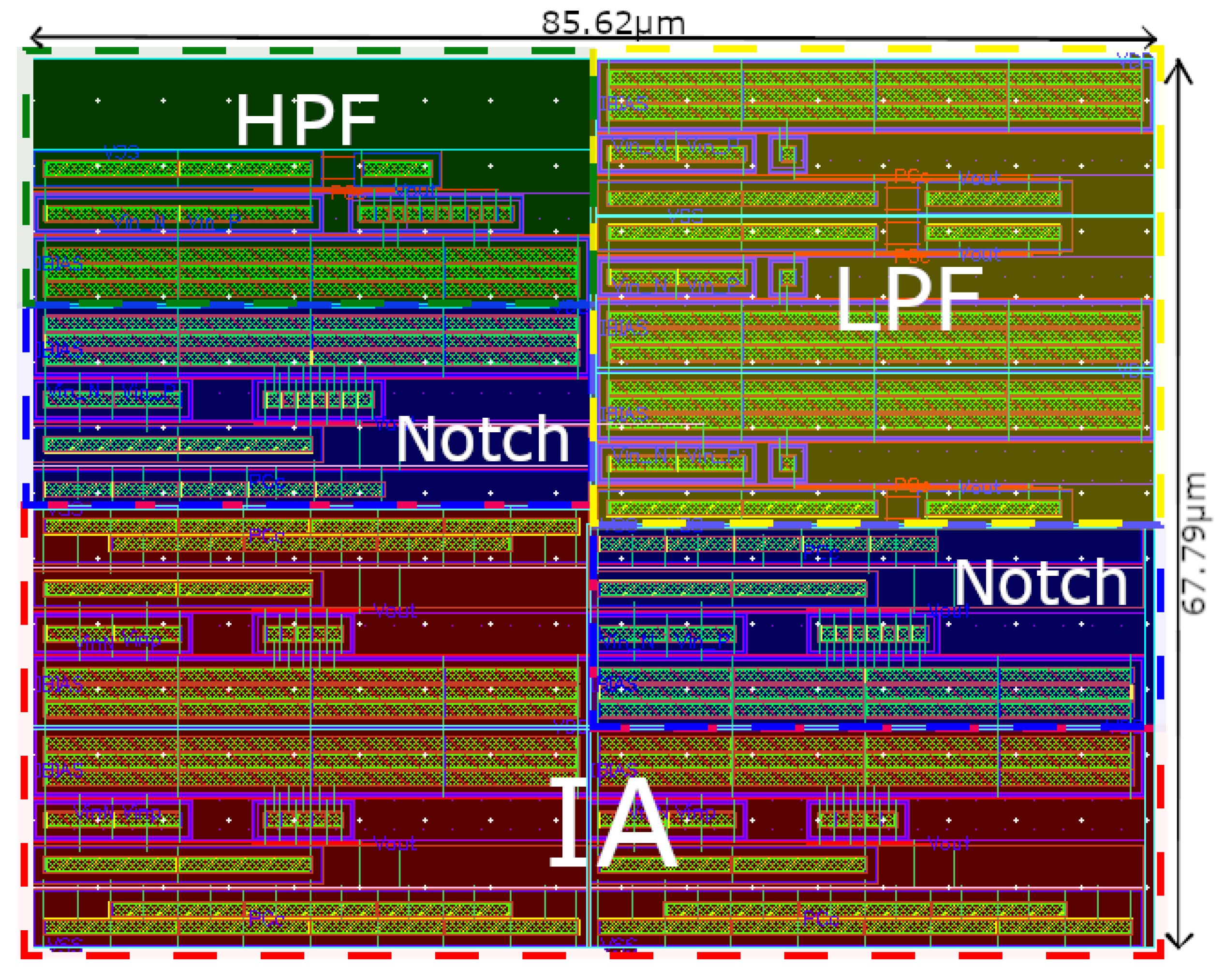
Figure 37 demonstrates the post-layout frequency response of the ECG acquisition system, where no significant changes are observed. The new bandwidth is approximately 239 Hz, which is only 7 Hz lower than that obtained from the schematic-level simulation.
Figure 38 verifies a good similarity in noise performance with the pre-layout simulation. This justifies that the layout has less parasitic effects.
4.4. Comparison with State-of-the-Art Designs
Table 9 summarizes a comparison of the performance metrics with state-of-the-art designs for ECG acquisition systems. Among the mentioned works, this work utilizes the smallest technology node (45 nm). The order of the filter and gain of the system designed here are the highest among the reported works. This work has the smallest chip area, one of the best input-referred noise with power-line-interference removal capability. Rest of the parameters are comparable. These results highlight the fact that the methodology developed in this work can be utilized in designing OTA with reduced time and effort.
5. Conclusions
This paper focuses on the design flow for a low power, low noise and a high gain ECG acquisition system. A two stage OTA is successfully designed using the developed methodology. All the blocks are designed and simulated separately. Finally they are cascaded to form the band pass filter with a notch (ECG system) to remove power line interference (PLI). The designed ECG acquisition system is simulated at T=27o C using TSMC 45nm technology in Cadence virtuoso. DC, AC, transient, power, CMRR, PSRR, noise, pole-zero and THD are analyzed. The design is layouted and to fortify confidence in the design, post layout simulations after parasitic extraction (PEX) are done. The AFE successfully de-noised a noisy ECG signal (MIT-BIH dataset). Comparison of the performance metrics with state-of-the designs for both the OTA and the ECG acquisition system implemented in this work shows their superiority considering the lowest technology node used herein. Therefore, the proposed design in this work has excellent promises in the realization of ECG acquisition system for the modern healthcare.
Author Contributions
Conceptualization, M.Z.A.E. and M.I.B.C.; methodology, M.Z.A.E.; software, M.Z.A.E.; validation, M.Z.A.E. and M.I.B.C.; formal analysis, M.Z.A.E. and M.I.B.C.; investigation, M.Z.A.E.; resources, M.Z.A.E.; data curation, M.Z.A.E.; writing—original draft preparation, M.Z.A.E.; writing—review and editing, M.I.B.C. and K.M.S.; visualization, M.Z.A.E.; supervision, M.I.B.C.; project administration, K.M.S.; funding acquisition, M.Z.A.E. and K.M.S. All authors have read and agreed to the published version of the manuscript.
Funding
Funded by Institute for Advanced Research Publication Grant of United International University, Ref. No.: IAR-2024-Pub-027 and Independent University Bangladesh.
Data Availability Statement
Not applicable.
Conflicts of Interest
The authors declare no conflict of interest.
Abbreviations
The following abbreviations are used in this manuscript:
| TSMC | Taiwan Semiconductor Manufacturing Company |
| MOSFET | Metal Oxide Semi-conductor Field Effect Transistor |
| OTA | Operational Trans-conductance Amplifier |
| OPAMP | Operational Amplifier |
| IA | Instrumentation Amplifier |
| ECG | Electrocardiogram |
| CMRR | Common-Mode Rejection Ratio |
| PSRR | Power Supply Rejection Ratio |
| PEX | Parasitic Extraction |
| GBW | Gain Band Width Product |
| SR | Slew Rate |
| PVS | Physical Verification System |
| QRC | Quantus RC Extraction |
| IRN | Input-referred noise |
| PVT | Process, Variation and Temperature |
Appendix A
; //SAMPLE OCEAN-SCRIPT FOR GM/ID CURVE GENERATION//
; DESIGN, RESULT, DEFINITION, MODEL FILE DIRECTORY
simulator( ’spectre )
design( "/home/simulation/pmos_char/spectre/schematic/netlist/netlist")
resultsDir( "/home/simulation/pmos_char/spectre/schematic" )
modelFile(
’("/pkg/eee/cadence/tech/gpdk045_v_5_0/..
/models/spectre/gpdk045.scs" "mc")
)
definitionFile(
"/home/work/save_op.scs"
)
;DC SWEEP
analysis(’dc ?saveOppoint t ?dev "/V0" ?param "dc"
?start ".1" ?stop ".6" ?lin "50" )
desVar( "half_supply" 300m ) ; M1, M2
desVar( "length" 45n )
desVar( "width" 1u )
envOption(
’firstRun t
’analysisOrder list("dc")
)
temp( 27 ) ; TEMPERATURE SET TO 27
;PARAMETRIC ANALYSIS - ‘length’ VARIED
paramAnalysis("length" ?values ’(4.95e-07
1e-06 5e-06 10e-06)
)
paramRun()
;PARAMETER EQUATIONS
gmoverId =((-getData("M0:gm" ?result "dc"))/getData("M0:id" ?result "dc"))
Id = (- getData("M0:id" ?result "dc"))
;CROSS-PLOTTING
newWindow()
ocnYvsYplot(?wavex Id ?wavey gmoverId)
awvLogXAxis(currentWindow() t)
awvSetXAxisLabel(currentWindow() "Id")
awvSetYAxisLabel(currentWindow() 1 "gm/Id")
addSubwindowTitle("pMOS - gm/Id vs Id")
;//Script finish//
References
- Samsung. Samsung Begins Chip Production Using 3nm Process Technology With GAA Architecture. Press Release, 30 June 2022.
- TSMC. TSMC Holds 3nm Volume Production and Capacity Expansion Ceremony, Marking a Key Milestone for Advanced Manufacturing. Press Release, 29 December 2022.
- Li, Y.; Zhi, W.; Li, Y.; Zhou, J.; Hong, Z.; Xu, J. A 15.5-ENOB 335 mVPP-Linear-Input-Range 4.7-GΩ-Input-Impedance CT-Δ∑M Analog Front-End With Embedded Low-Frequency Chopping. IEEE Solid-State Circuits Letters 2023, 6, 265–268. [Google Scholar] [CrossRef]
- Khateb, F.; Prommee, P.; Kulej, T. MIOTA-Based Filters for Noise and Motion Artifact Reductions in Biosignal Acquisition. IEEE Access 2022, 10, 14325–14338. [Google Scholar] [CrossRef]
- Sin, S.W.; U, S.P.; Martins, R. Novel low-voltage circuit techniques for fully-differential reset- and switched-opamps. Research in Microelectronics and Electronics, 2005 PhD, 2005, Vol. 2, pp. 194–197. [CrossRef]
- Toledo, P.; Crovetti, P.S.; Klimach, H.D.; Musolino, F.; Bampi, S. Low-Voltage, Low-Area, nW-Power CMOS Digital-Based Biosignal Amplifier. IEEE Access 2022, 10, 44106–44115. [Google Scholar] [CrossRef]
- Wang, Y.; Zhang, Q.; Yu, S.S.; Zhao, X.; Trinh, H.; Shi, P. A Robust Local Positive Feedback Based Performance Enhancement Strategy for Non-Recycling Folded Cascode OTA. IEEE Transactions on Circuits and Systems I: Regular Papers 2020, 67, 2897–2908. [Google Scholar] [CrossRef]
- Rico-Aniles, H.D.; Ramirez-Angulo, J.; Rocha-Perez, J.M.; Lopez-Martin, A.J.; Carvajal, R.G. Low-Voltage 0.81mW, 1–32 CMOS VGA With 5% Bandwidth Variations and -38dB DC Rejection. IEEE Access 2020, 8, 106310–106321. [Google Scholar] [CrossRef]
- V. Soman, K.K.G.; Baskaran, M. V. Soman, K.K.G.; Baskaran, M. Analysis and Design of a Two stage Telescopic OTA using SCL 180nm CMOS Technology, 2023. 2023 International Conference on Networking and Communications (ICNWC), Chennai, India, 2023, pp. 1-6. [CrossRef]
- P, A.K.; Rajeev, S.P. Performance Assessment of Two Stage Operational Transconductance Amplifier in 180nm with Optimised Compensation Capacitance and Nulling Resistor, 2021. 2021 5th International Conference on Electronics, Communication and Aerospace Technology (ICECA), Coimbatore, India, 2021, pp. 279-285. [CrossRef]
- Shaber, M.U.; Signell, S. Fully differential gain-boosted ota design for pipeline DA-converter in 180nm CMOS technology. 2005 12th IEEE International Conference on Electronics, Circuits and Systems, 2005, pp. 1–4. [CrossRef]
- O’Rourke, D.; Abdel-Aty-Zohdy, H. An operational transconductance amplifier in 0.18/spl mu/m SOI. 48th Midwest Symposium on Circuits and Systems, 2005., 2005, pp. 5–8 Vol. 1. [CrossRef]
- Bozomitu, R.G.; Cojan, N.; Bonteanu, G. A VLSI implementation of the 4th order elliptic fully differential IIR switched-capacitor low-pass filter in CMOS technology. 2013 IEEE 19th International Symposium for Design and Technology in Electronic Packaging (SIITME), 2013, pp. 85–88. [CrossRef]
- Adimulam, M.K.; Divya, A.; Tejaswi, K.; Srinivas, M. A low power, low noise Programmable Analog Front End (PAFE) for biopotential measurements. 2017 39th Annual International Conference of the IEEE Engineering in Medicine and Biology Society (EMBC), 2017, pp. 3844–3847. [CrossRef]
- Ardakani, H.A.; Dehghani, R.; Asgari, V. A compensation strategy for two-stage operational transconductance amplifiers based on zero splitting. 2014 22nd Iranian Conference on Electrical Engineering (ICEE), 2014, pp. 491–495. [CrossRef]
- Shen, J.; Zhang, Y.; Zhou, Y. A High-Gain Low-Power Low-Noise CMOS Transconductance Amplifier. 2023 IEEE 5th International Conference on Power, Intelligent Computing and Systems (ICPICS), 2023, pp. 1194–1200. [CrossRef]
- Jacob Baker, H.W.L.; Boyce, D.E. CMOS, Circuit Design, Layout, and Simulation; JOHN WILEY & SONS, INC., PUBLICATION: River Street Hoboken, NJ, 2010.
- Zhang, J.; Zhang, H.; Sun, Q.; Zhang, R. A Low-Noise, Low-Power Amplifier With Current-Reused OTA for ECG Recordings. IEEE Transactions on Biomedical Circuits and Systems 2018, 12, 700–708. [Google Scholar] [CrossRef]
- Lee, C.J.; Song, J.I. A Chopper-Stabilized Amplifier With a Tunable Bandwidth for EEG Acquisition Applications. IEEE Access 2019, 7, 73165–73171. [Google Scholar] [CrossRef]
- Khateb, F.; Kulej, T.; Akbari, M.; Kumngern, M. 0.5-V High Linear and Wide Tunable OTA for Biomedical Applications. IEEE Access 2021, 9, 103784–103794. [Google Scholar] [CrossRef]
- Gangineni, M.; Ramirez-Angulo, J.; Vázquez-Leal, H.; Huerta-Chua, J.; Lopez-Martin, A.J.; Carvajal, R.G. 0.3V Bulk-Driven Fully Differential Buffer with High Figures of Merit. Journal of Low Power Electronics and Applications 2022, 12. [Google Scholar] [CrossRef]
- Mao, P.; Li, H.; Yu, Z. A Review of Skin-Wearable Sensors for Non-Invasive Health Monitoring Applications. Sensors 2023, 23. [Google Scholar] [CrossRef]
- Chow, H.C.; Weng, P.N. A Low Voltage Rail-to-Rail OPAMP Design for Biomedical Signal Filtering Applications. 4th IEEE International Symposium on Electronic Design, Test and Applications (delta 2008), 2008, pp. 232–235. [CrossRef]
- J. M. Algueta Miguel, A. J. J. M. Algueta Miguel, A. J. López-Martín, C.J.R.A.; Carvajal, R.G. CMOS op-amps for biomedical applications, 2014. IEEE International Symposium on Circuits and Systems (ISCAS), Melbourne, VIC, Australia, 2014, pp. 1364-1367. [CrossRef]
- Kavyashree, C.L.; Hemambika, M.; Dharani, K.; Naik, A.V.; Sunil, M.P. Design and implementation of two stage CMOS operational amplifier using 90nm technology. 2017 International Conference on Inventive Systems and Control (ICISC), 2017, pp. 1–4. [CrossRef]
- Nagulapalli, R.; Hayatleh, K.; Barker, S.; Reddy, B.N.K. A two-stage opamp frequency Compensation technique by splitting the 2nd stage. 2020 11th International Conference on Computing, Communication and Networking Technologies (ICCCNT), 2020, pp. 1–5. [CrossRef]
- Emon, M.Z.A.; Chowdhury, M.I.B. Low Threshold Voltage MOSFET - A Potential Candidate for Biomedical IC Design. 2024 International Conference on Advances in Computing, Communication, Electrical, and Smart Systems (iCACCESS), 2024, pp. 1–6. [CrossRef]
- Jespers, P. The gm/ID Methodology, a sizing tool for low-voltage analog CMOS Circuits: The semi-empirical and compact model approaches; Springer: 233 Spring Street, New York, NY 10013, USA, 2010.
- Allen, P.E.; Holberg, D.R. CMOS Analog Circuit Design; Oxford University Press, Inc: 198 Madison Avenue, New York, NY 10016, 2012.
- Noulis, T., P.C..H.A.E. SMART Integrated Circuit Design and Methodology; River Publishers: New York, 2023. [CrossRef]
- Mostafa, N. Sabry, H.O.; Dessouky, M. Systematic Design and Optimization of Operational Transconductance Amplifier Using gm/ID Design Methodology. Microelectronics Journal 2018, 75, 87–96. [Google Scholar] [CrossRef]
- Saidulu, B.; Manoharan, A.; Sundaram, K. Low Noise Low Power CMOS Telescopic-OTA for Bio-Medical Applications. Computers 2016, 5. [Google Scholar] [CrossRef]
- Jin, Y.; Seo, Y.; Kim, S.; Cho, S. Three-Stage Operational Amplifier with Frequency Compensation Using Cascade Zero. Electronics 2023, 12. [Google Scholar] [CrossRef]
- Tony Chan Carusone, D.A.J.; Martin, K.W. ANALOG INTEGRATED CIRCUIT DESIGN; John Wiley & Sons, Inc.: 111 River Street, Hoboken, NJ 07030-5774, (201)748-6011, 2012.
- Mahmoud, S.A., B. A.; Al-Tunaiji, S. Low-Noise Low-Pass Filter for ECG Portable Detection Systems with Digitally Programmable Range. Circuits Syst Signal Process 2013, 32, 2029–2045. [Google Scholar] [CrossRef]
- Razavi, B. Design of Analog CMOS Integrated Circuits; McGraw-Hill Education: 2 Penn Plaza, New York, NY 10121, 2017.
- O, K.; Park, N.; Yang, D.J. 1/f noise of NMOS and PMOS transistors and their implications to design of voltage controlled oscillators. 2002 IEEE Radio Frequency Integrated Circuits (RFIC) Symposium. Digest of Papers (Cat. No.02CH37280), 2002, pp. 59–62. [CrossRef]
- Bastos, J.; Steyaert, M.; Roovers, R.; Kinget, P.; Sansen, W.; Graindourze, B.; Pergoot, A.; Janssens, E. Mismatch characterization of small size MOS transistors. Proceedings International Conference on Microelectronic Test Structures, 1995, pp. 271–276. [CrossRef]
- Yodprasit, U.; Ngarmnil, J. Efficient low-power designs using MOSFETs in the weak inversion region. IEEE. APCCAS 1998. 1998 IEEE Asia-Pacific Conference on Circuits and Systems. Microelectronics and Integrating Systems. Proceedings (Cat. No.98EX242), 1998, pp. 45–48. [CrossRef]
- Tajalli, A.; Alioto, M.; Leblebici, Y. Improving Power-Delay Performance of Ultra-Low-Power Subthreshold SCL Circuits. IEEE Transactions on Circuits and Systems II: Express Briefs 2009, 56, 127–131. [Google Scholar] [CrossRef]
- Furman, S.; Hurzeler, P.D.V. The ventricular endocardial electrogram and pacemaker sensing. The Journal of thoracic and cardiovascular surgery. 1977, 73, 258–266. [Google Scholar] [CrossRef] [PubMed]
- John G. Webster, A.J.N. Medical Instrumentation: Application and Design; John Wiley & Sons, Inc.: 111 River Street, Hoboken, NJ 07030-5774, (201)748-6011, 2020.
- Xie, L.; Li, Z.; Zhou, Y.; He, Y.; Zhu, J. Computational Diagnostic Techniques for Electrocardiogram Signal Analysis. Sensors 2020, 20. [Google Scholar] [CrossRef] [PubMed]
- Company-Bosch, E.; Hartmann, E. ECG Front-End Design is Simplified with MicroConverter, 2003.
- Silva, C.V.; Philominraj, A.; del Rio, C. A DSP Practical Application: Working on ECG Signal. In Applications of Digital Signal Processing; Cuadrado-Laborde, C., Ed.; IntechOpen: Rijeka, 2011; chapter 8. [CrossRef]
- Chow, H.C.; Wang, J.Y. High CMRR instrumentation amplifier for biomedical applications. 2007 9th International Symposium on Signal Processing and Its Applications, 2007, pp. 1–4. [CrossRef]
- Tereshchenko, L.G.; Josephson, M.E. Frequency content and characteristics of ventricular conduction. Journal of electrocardiology 2015, 48. [Google Scholar] [CrossRef] [PubMed]
- Aspuru, J.; Ochoa-Brust, A.; Félix, R.A.; Mata-López, W.; Mena, L.J.; Ostos, R.; Martínez-Peláez, R. Segmentation of the ECG Signal by Means of a Linear Regression Algorithm. Sensors 2019, 19. [Google Scholar] [CrossRef]
- Algueta-Miguel, J.M.; De La Cruz Blas, C.A.; Lopez-Martin, A.J. Balanced Gm-C filters with improved linearity and power efficiency. International Journal of Circuit Theory and Applications 2015, 43, 1147–1166. [Google Scholar] [CrossRef]
- Thyagarajan, S.V.; Pavan, S.; Sankar, P. Active-RC Filters Using the Gm-Assisted OTA-RC Technique. IEEE Journal of Solid-State Circuits 2011, 46, 1522–1533. [Google Scholar] [CrossRef]
- Sanabria-Borbon, A.C.; Sanchez-Sinencio, E. Efficient use of gain-bandwidth product in active filters: Gm-C and Active-R alternatives. 2017 IEEE 8th Latin American Symposium on Circuits & Systems (LASCAS), 2017, pp. 1–4. [CrossRef]
- Garcia-Alberdi, C., L. M.A.G.J.e.a. Low-Power Analog Channel Selection Filtering Techniques. Circuits Syst Signal Process 2017, 36, 895–915. [Google Scholar] [CrossRef]
- Badillo, I.; Portilla, J. Experimental Study of AM and PM Noise in Cascaded Amplifiers. Electronics 2022, 11. [Google Scholar] [CrossRef]
- Gayakwad, R. Op-amps and Linear Integrated Circuits; Prentice Hall, 2000.
- Mai, T.; Hagelauer, A.; Weigel, R. Maximizing Temperature and Process Corner Performance of Operational Amplifiers with a Novel Self-Adjusting Biasing Technique. 2018 Austrochip Workshop on Microelectronics (Austrochip), 2018, pp. 15–19. [CrossRef]
- Goldberger, A., L. A.L.G.J.H.P.C.I.R.M.J.E.M.G.B.M.C.K.P.; Stanley., H.E. PhysioBank, PhysioToolkit, and PhysioNet: Components of a new research resource for complex physiologic signals. Circulation [Online] 2000, 101, e215–e220. [Google Scholar] [CrossRef] [PubMed]
- Choi, G.; You, D.; Heo, H.; Kim, H.; Kwon, Y.; Nam, K.; Lee, S.; Ko, H. Current-Reused Current Feedback Instrumentation Amplifier for Low Power Leadless Pacemakers. IEEE Access 2021, 9, 113748–113758. [Google Scholar] [CrossRef]
- Liu, Z.; Tan, Y.; Li, H.; Jiang, H.; Liu, J.; Liao, H. A 0.5-V 3.69-nW Complementary Source-Follower-C Based Low-Pass Filter for Wearable Biomedical Applications. IEEE Transactions on Circuits and Systems I: Regular Papers 2020, 67, 4370–4381. [Google Scholar] [CrossRef]
- Kumngern, M.; Kulej, T.; Khateb, F. 31.3 nW, 0.5 V Bulk-Driven OTA for Biosignal Processing. IEEE Access 2023, 11, 56516–56525. [Google Scholar] [CrossRef]
- Lee, S.Y.; Wang, C.P.; Chu, Y.S. Low-Voltage OTA–C Filter With an Area- and Power-Efficient OTA for Biosignal Sensor Applications. IEEE Transactions on Biomedical Circuits and Systems 2019, 13, 56–67. [Google Scholar] [CrossRef]
Figure 1.
Typical block diagram of AFE for ECG signal acquisition
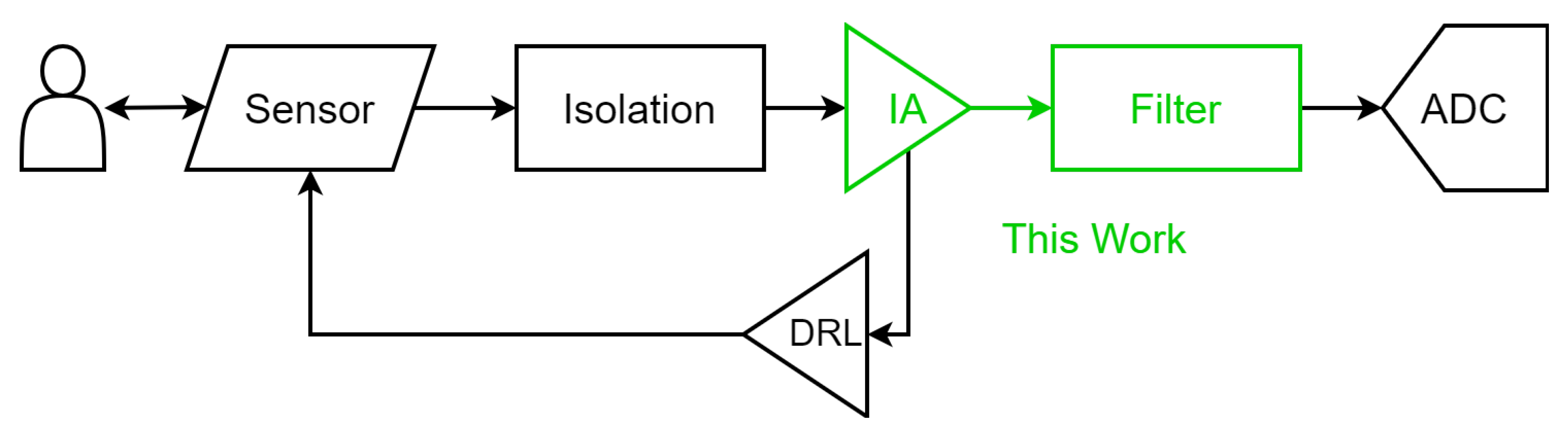
Figure 2.
Simplified block diagram of the work in this paper
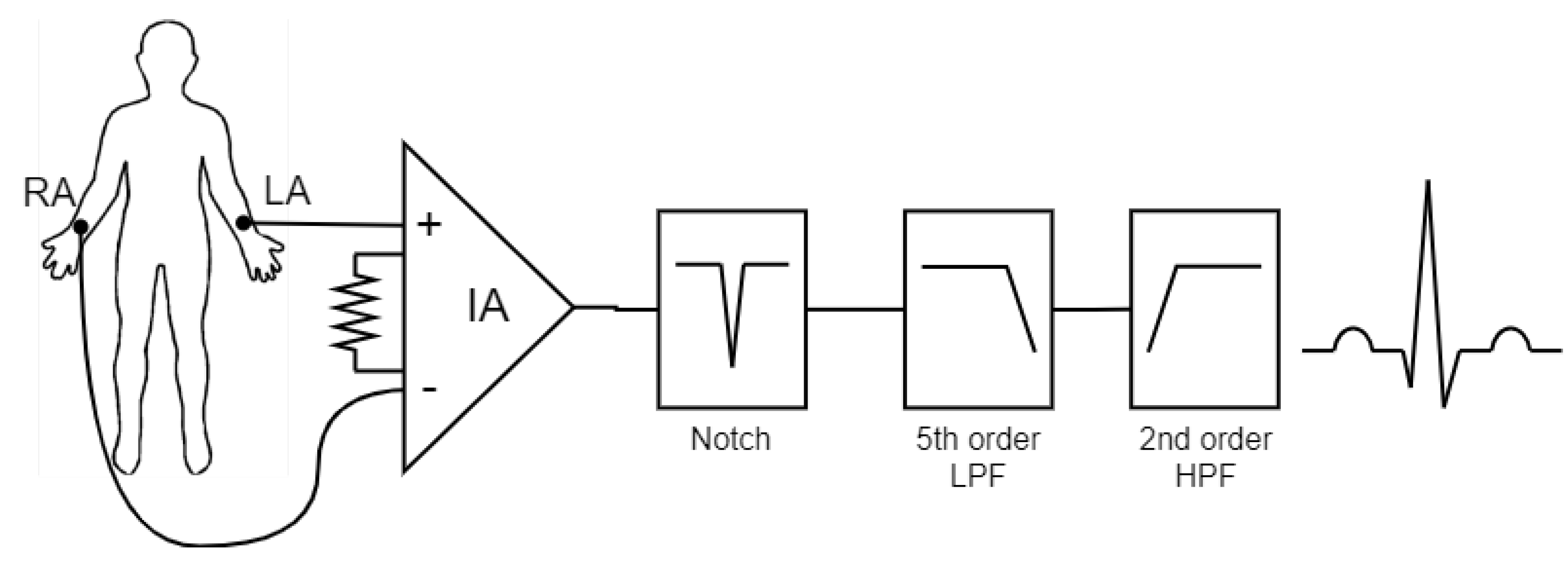
Figure 3.
Two stage OTA with Miller Compensation
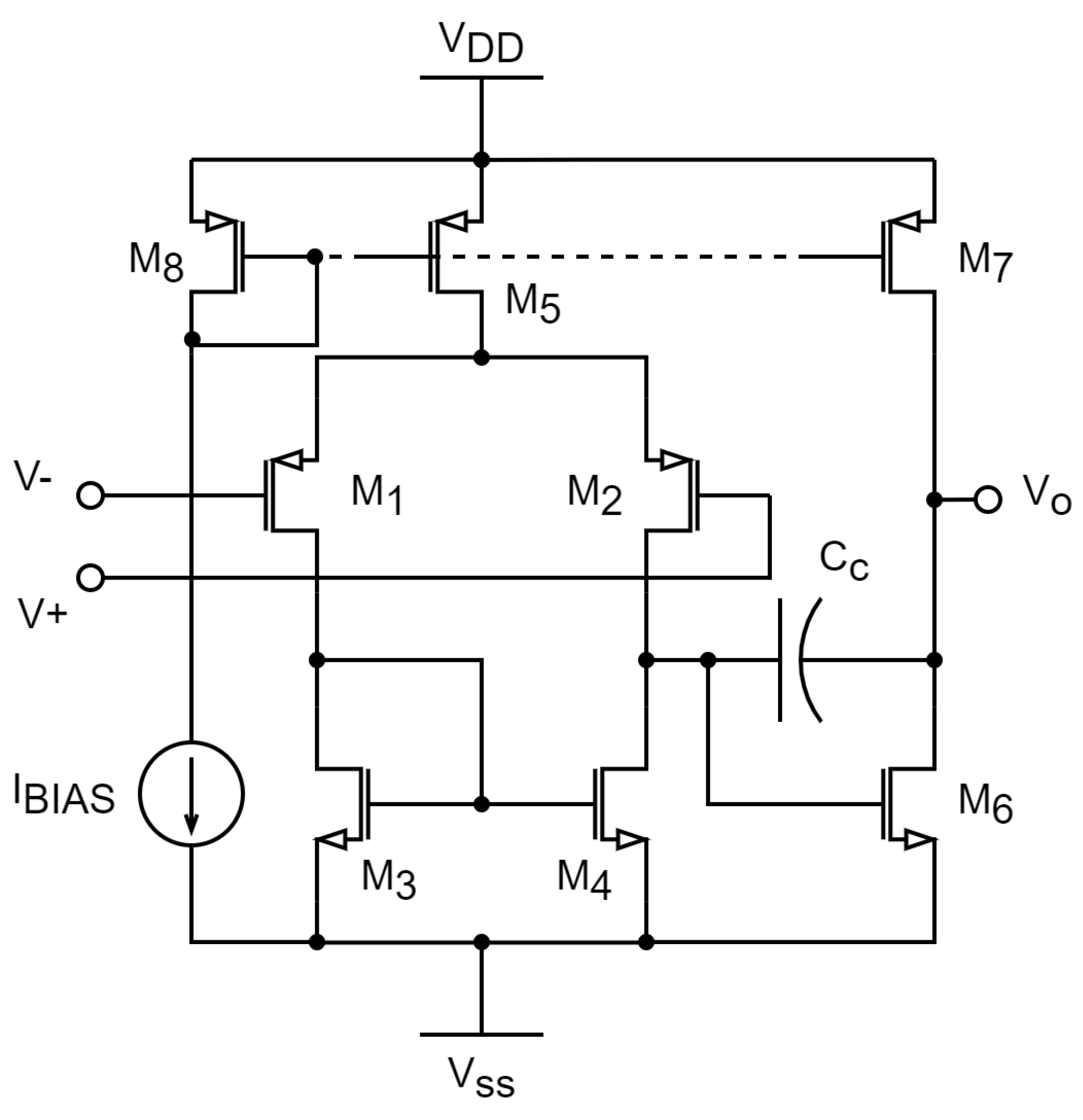
Figure 4.
Design flow for design and optimization of OTA.
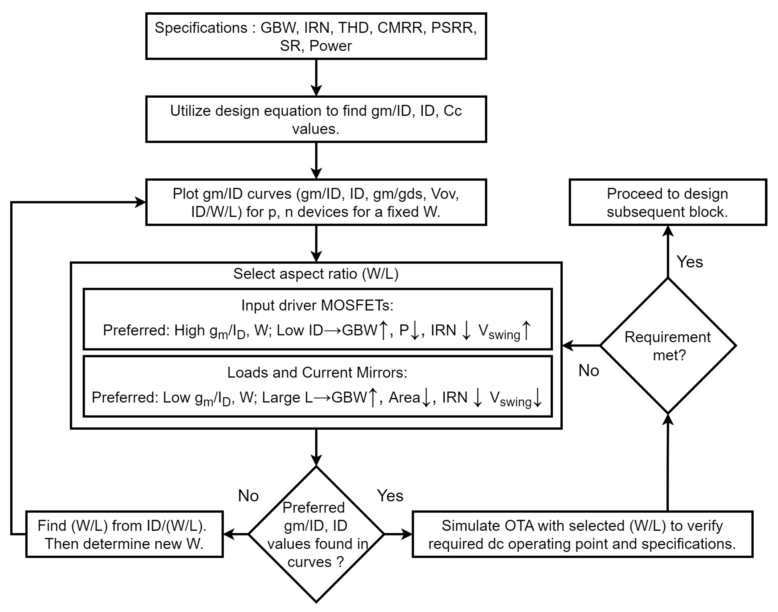
Figure 5.
Schematic diagrams for gm/ method curve generation. (Left) P- channel MOSFET. (Right) N-channel MOSFET.
Figure 5.
Schematic diagrams for gm/ method curve generation. (Left) P- channel MOSFET. (Right) N-channel MOSFET.
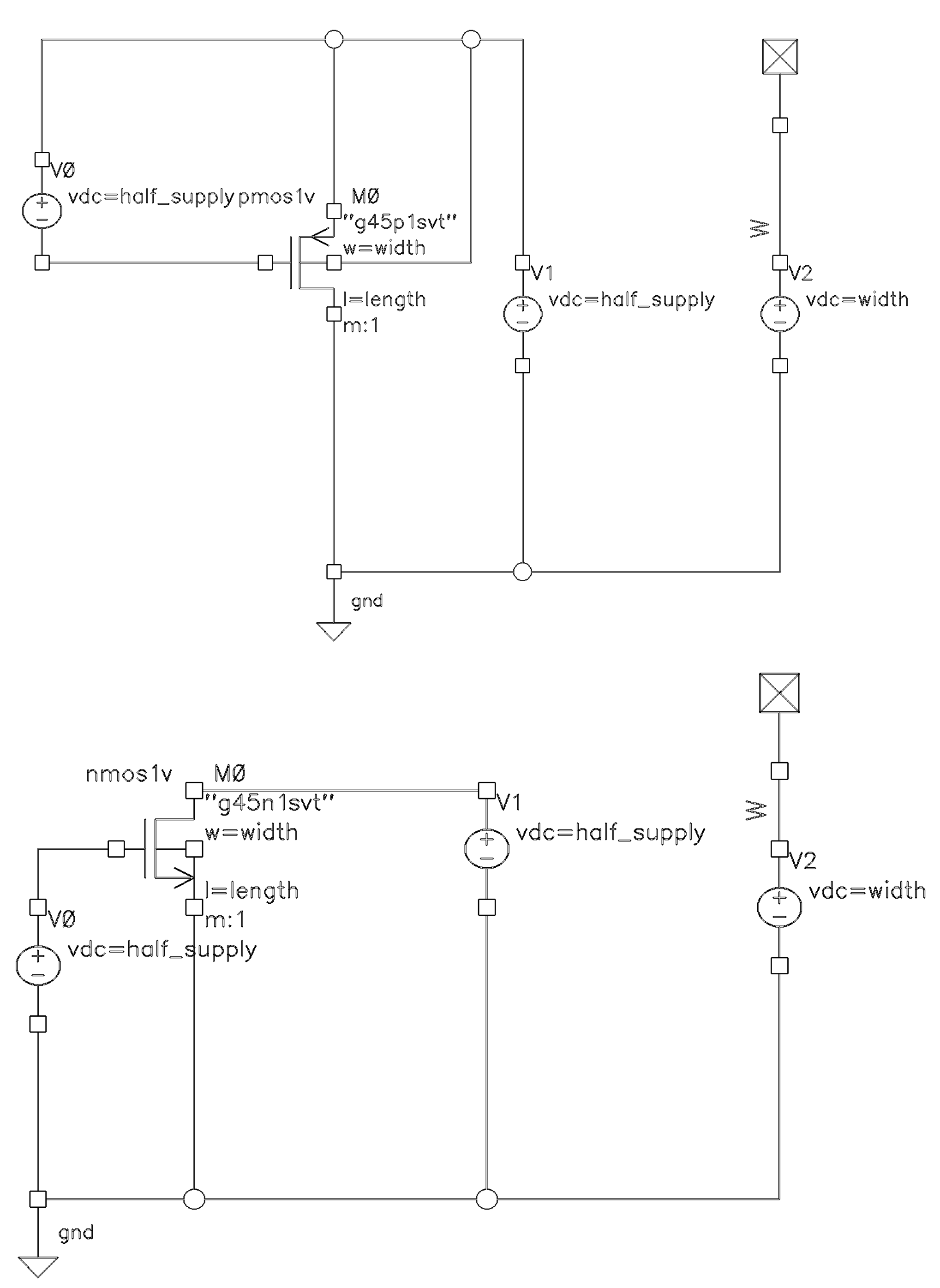
Figure 6.
vs Vov plot for p-channel MOS device at W=1 and L=1, 5, 10
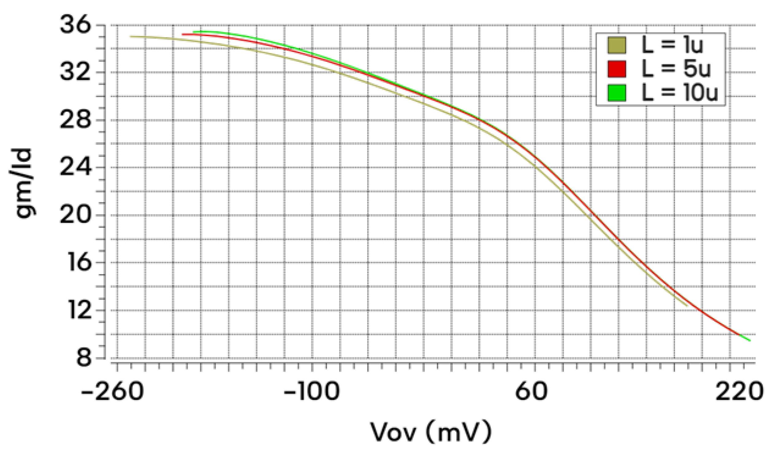
Figure 7.
Characteristic curves for the input pairs (). (a) vs for W=1 m. (b) vs for W=1 m. (c) vs Vov for W=1 m.
Figure 7.
Characteristic curves for the input pairs (). (a) vs for W=1 m. (b) vs for W=1 m. (c) vs Vov for W=1 m.
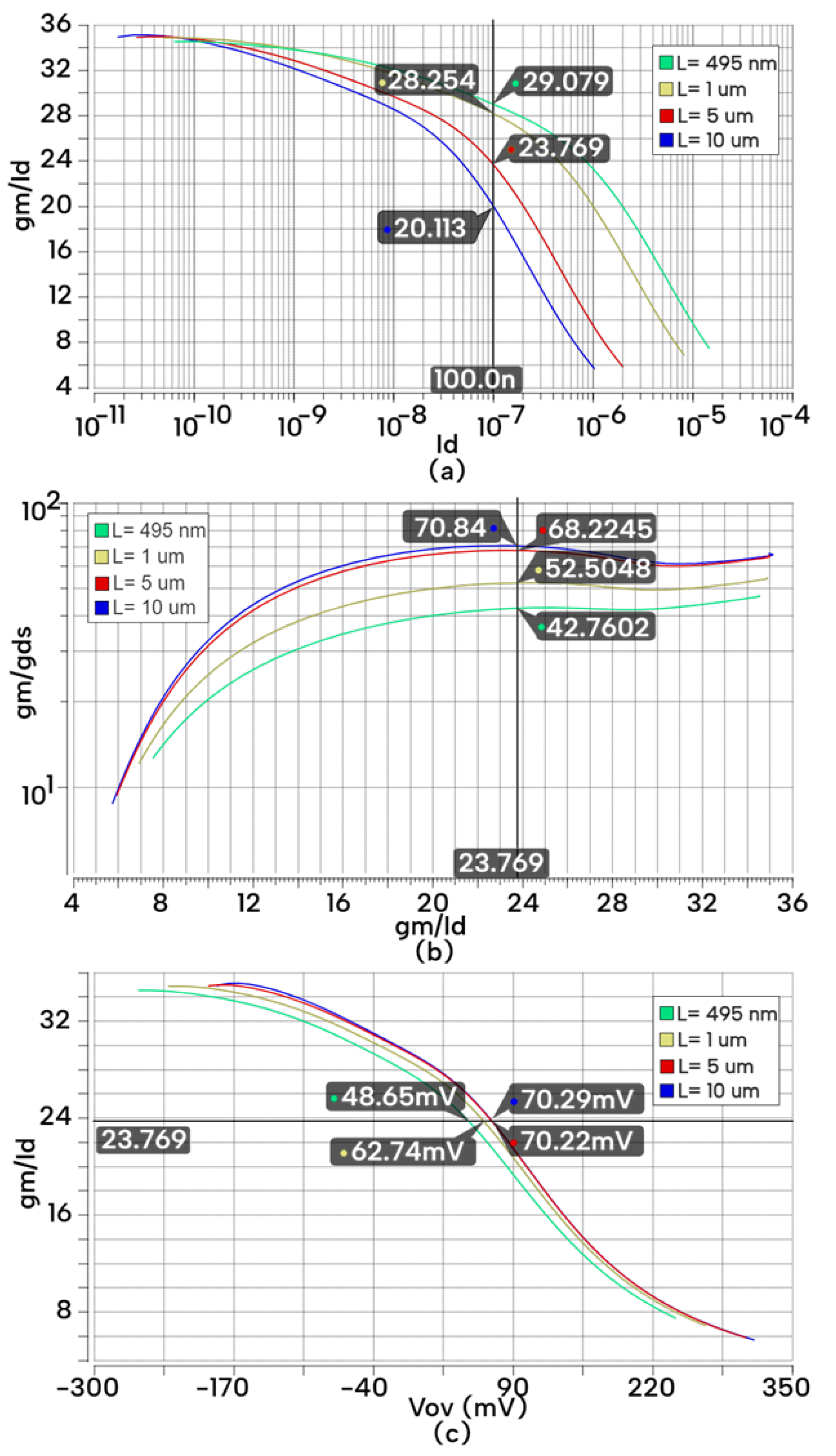
Figure 8.
Characteristic curves for the active loads (). (a) vs for W=1 m. (b) vs for W=1 m.
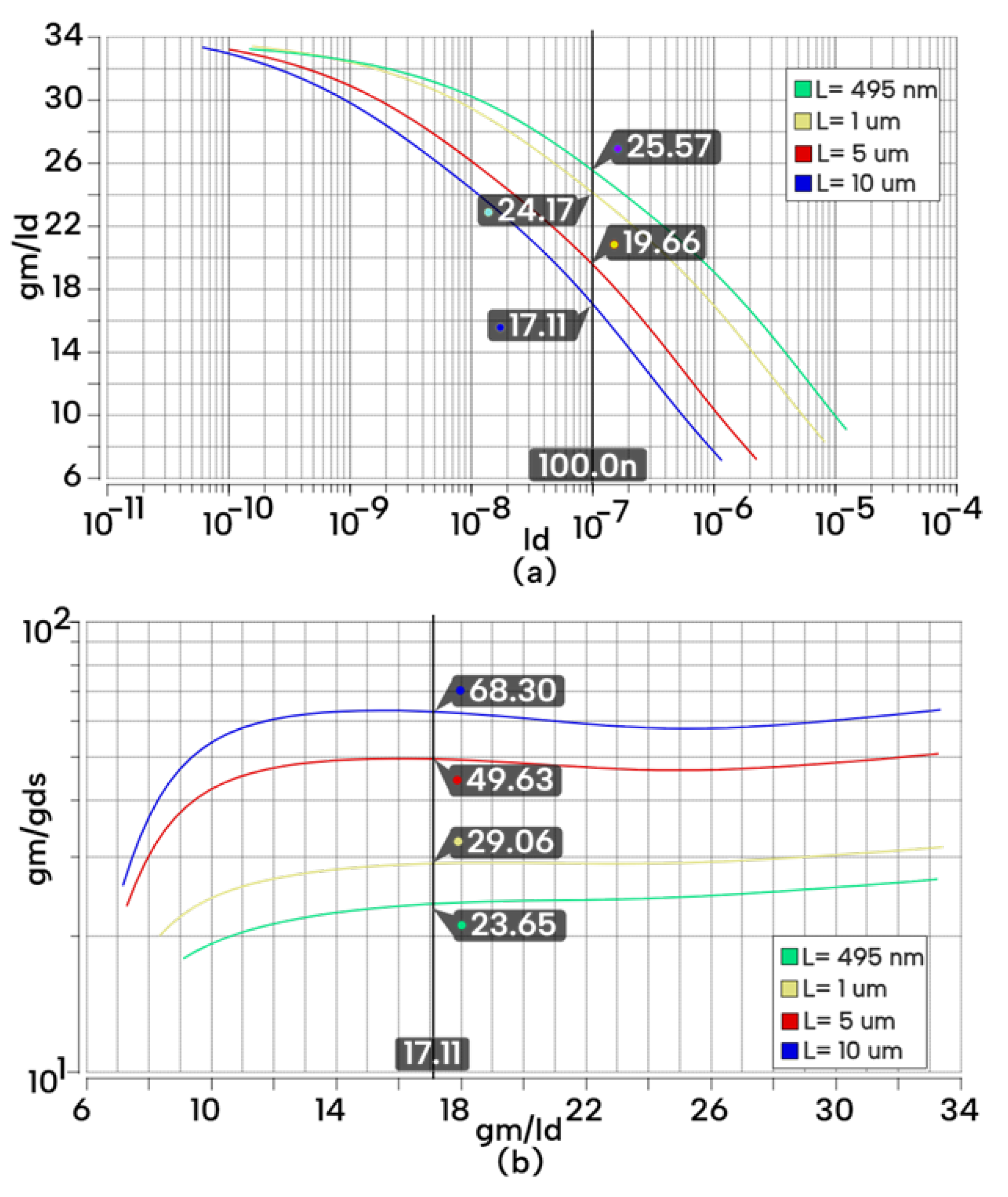
Figure 9.
Characteristic curves for and . (a) vs for W=1 m. (b) vs for W=1 m. (c) vs Vov for W=1 m.
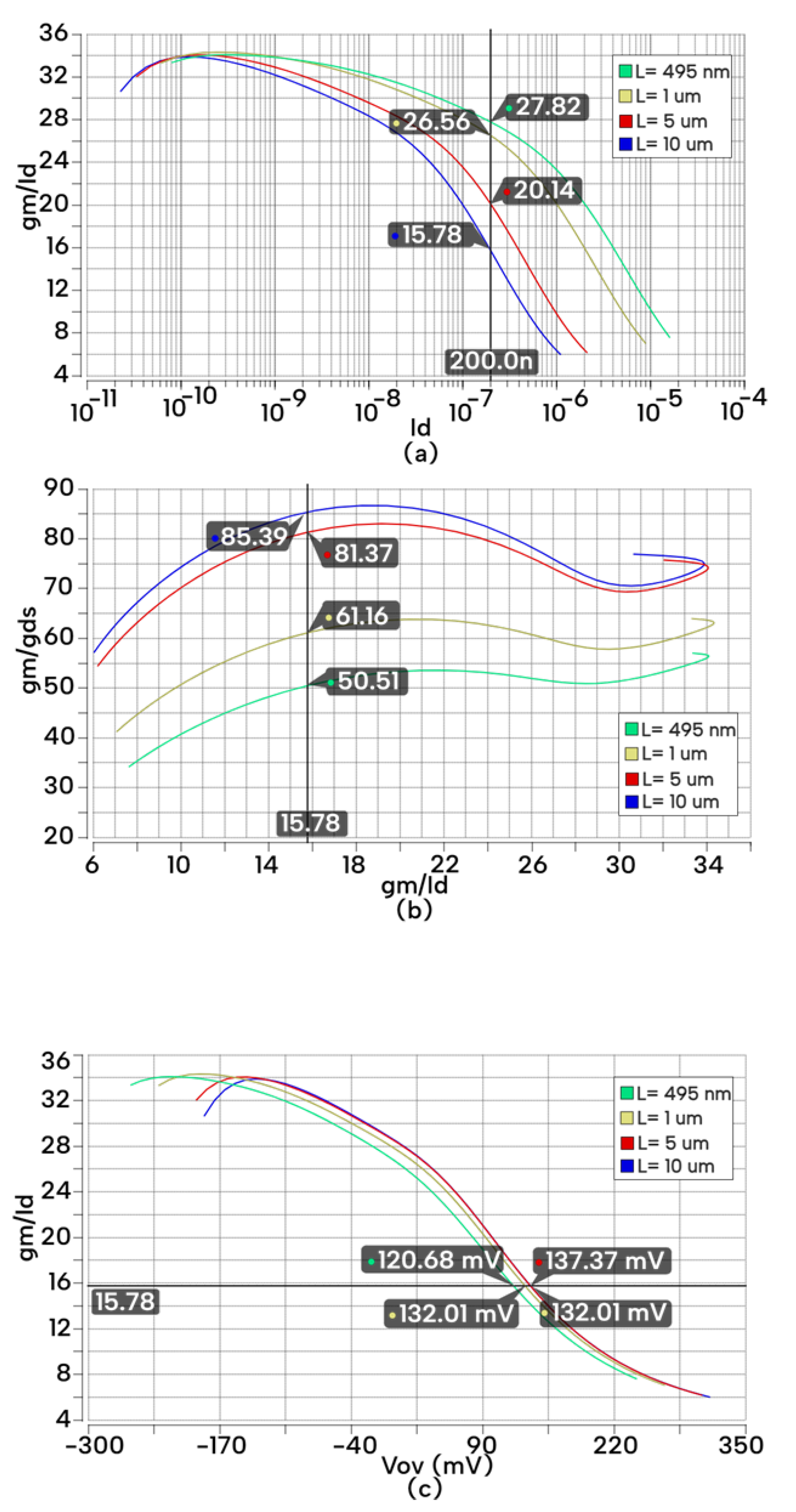
Figure 10.
Characteristic curves for the input driver (). (a) vs for W=1 m. (b) vs for W=1 m. (c) vs Vov for W=1 m.
Figure 10.
Characteristic curves for the input driver (). (a) vs for W=1 m. (b) vs for W=1 m. (c) vs Vov for W=1 m.
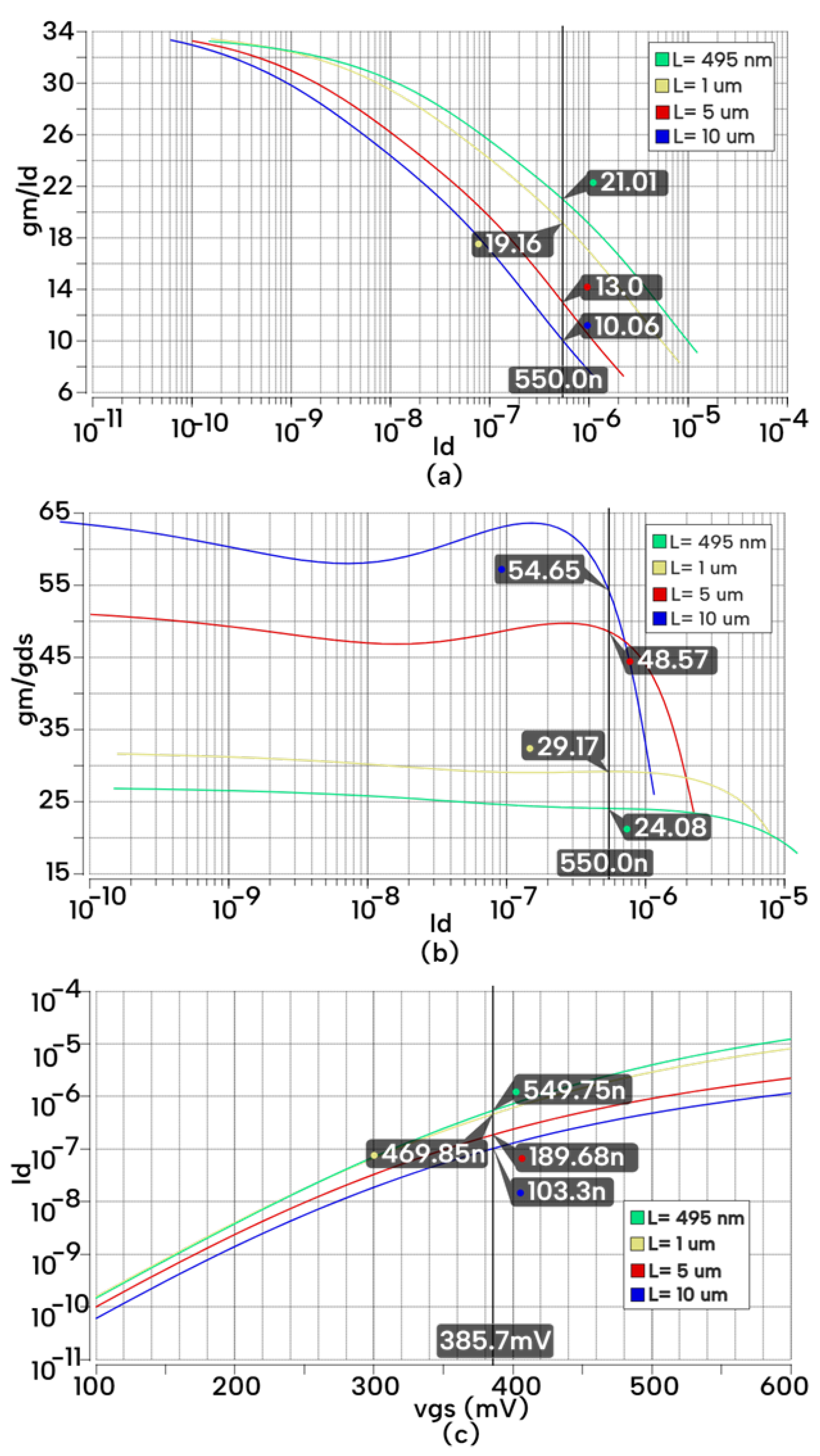
Figure 11.
(Characteristic curves for the active load (). a) vs for W=1 m. (b) vs for W=1 m. (c) vs Vgs for W=1 m.
Figure 11.
(Characteristic curves for the active load (). a) vs for W=1 m. (b) vs for W=1 m. (c) vs Vgs for W=1 m.
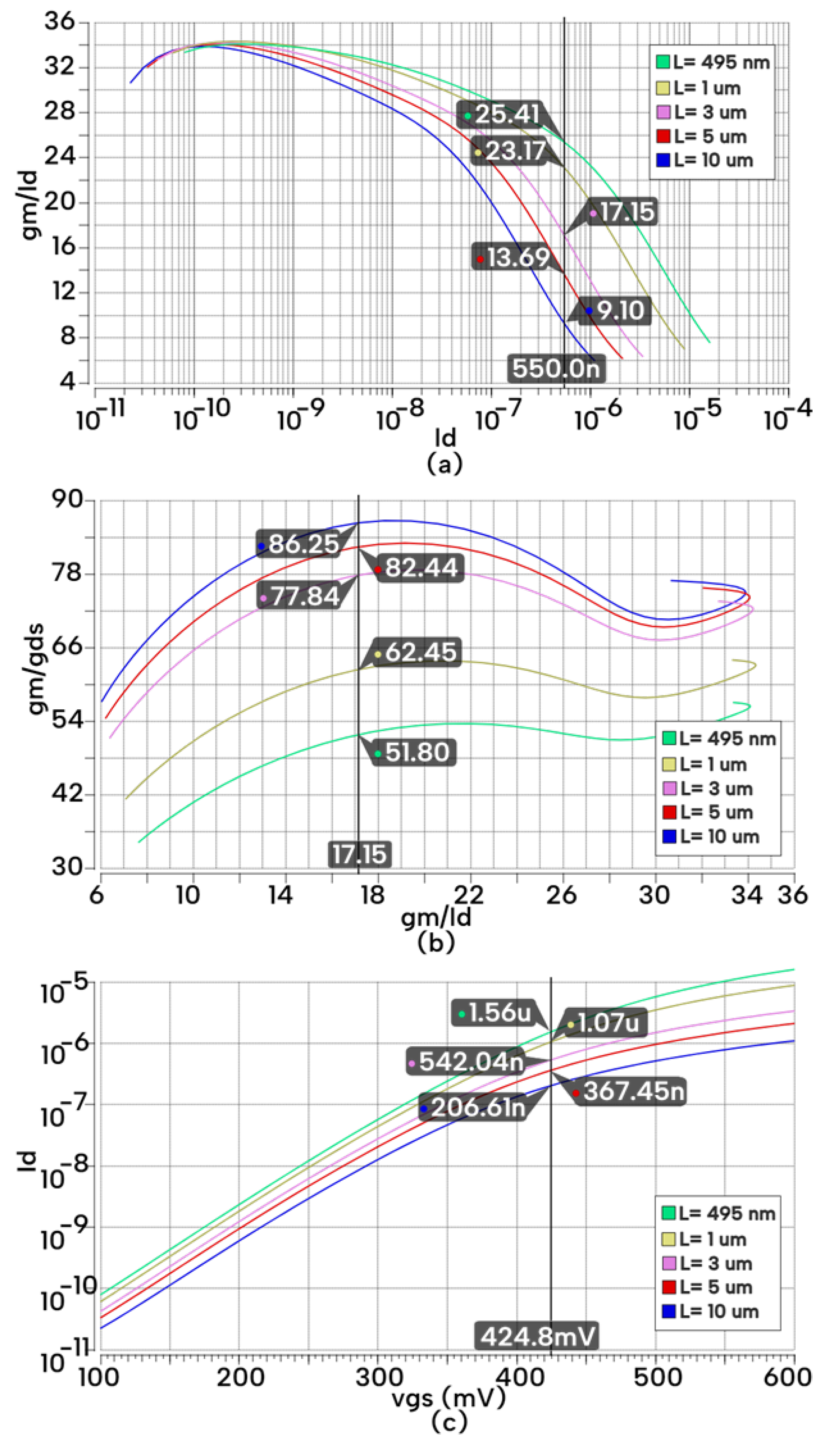
Figure 12.
Frequency response of designed OTA for the first iteration.
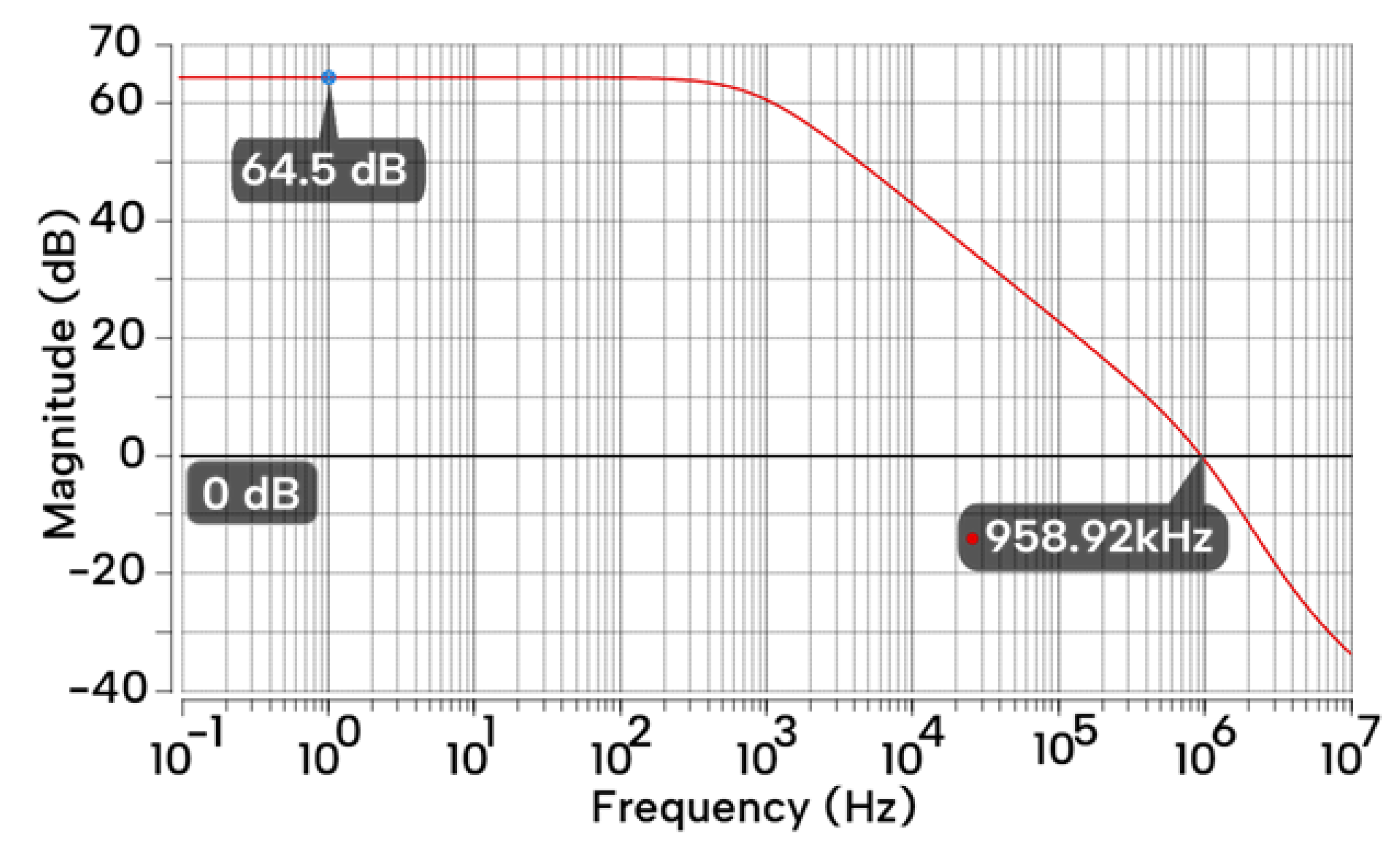
Figure 13.
DC operating points of the OTA circuit from simulation.
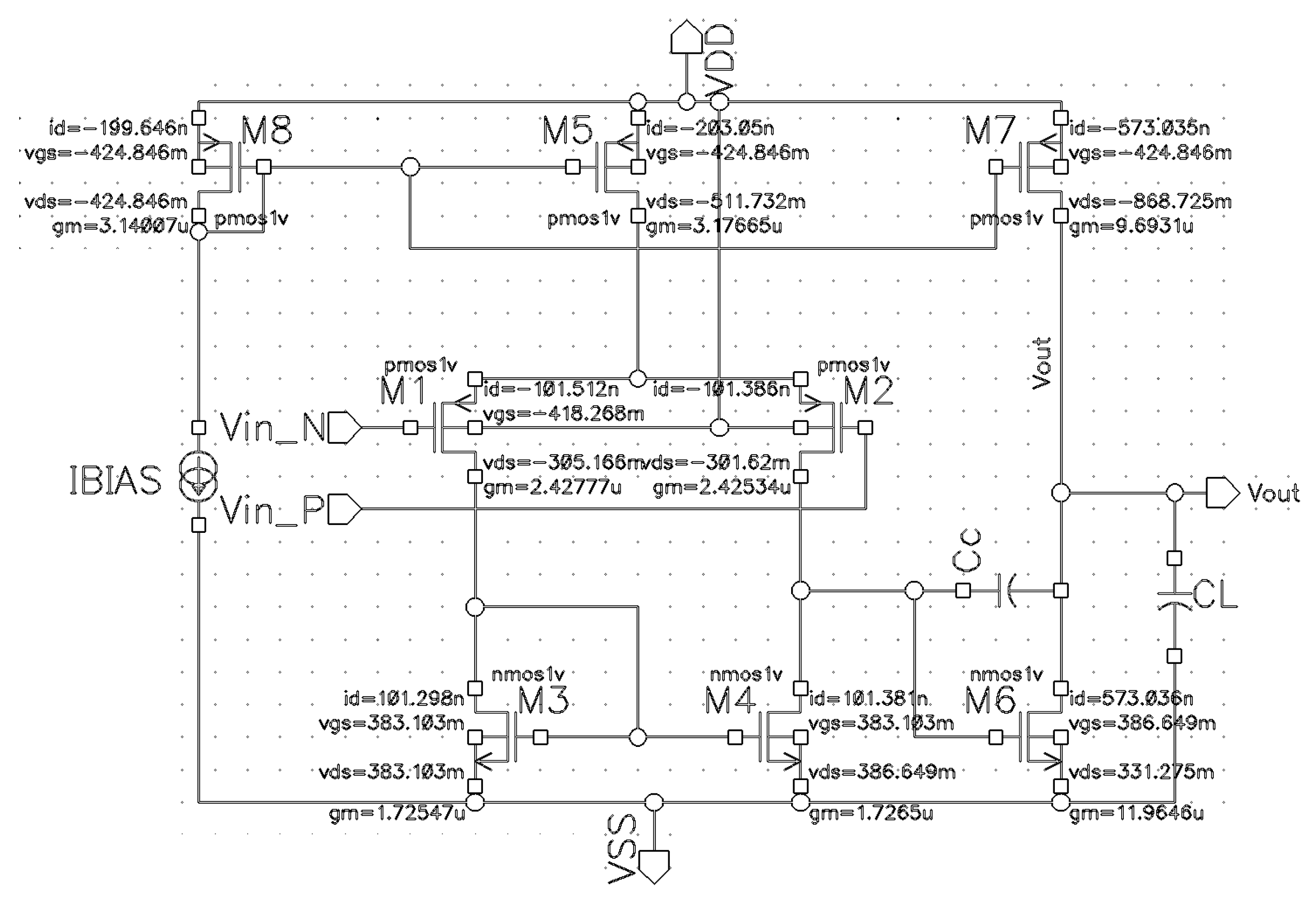
Figure 14.
, Vov and vs figures for p-channel MOS devices for W=1 m and L=5 m.
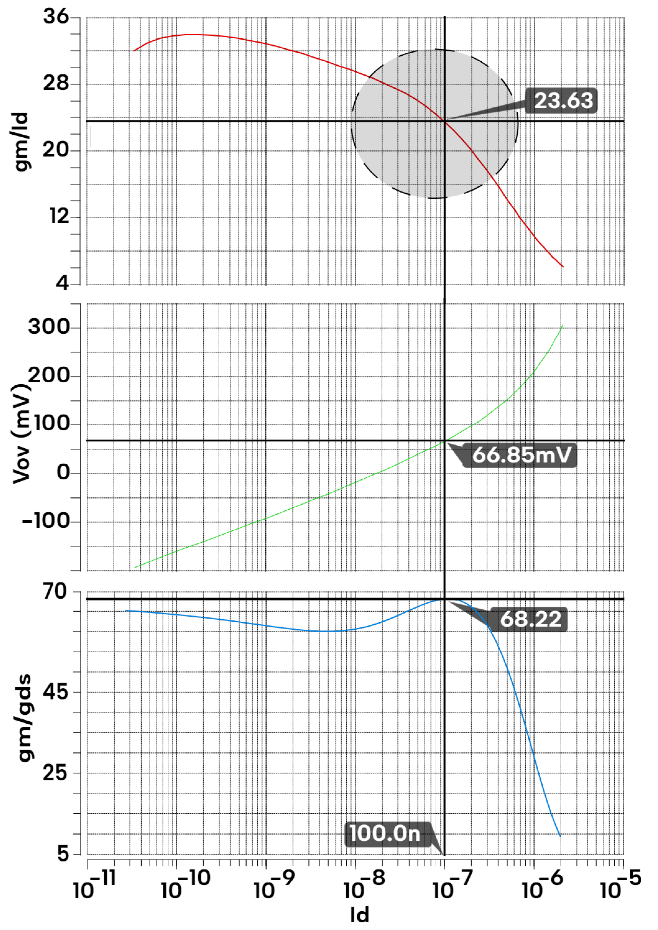
Figure 15.
ft x vs Vov plot for p-channel MOS device at W=1 and L=5.
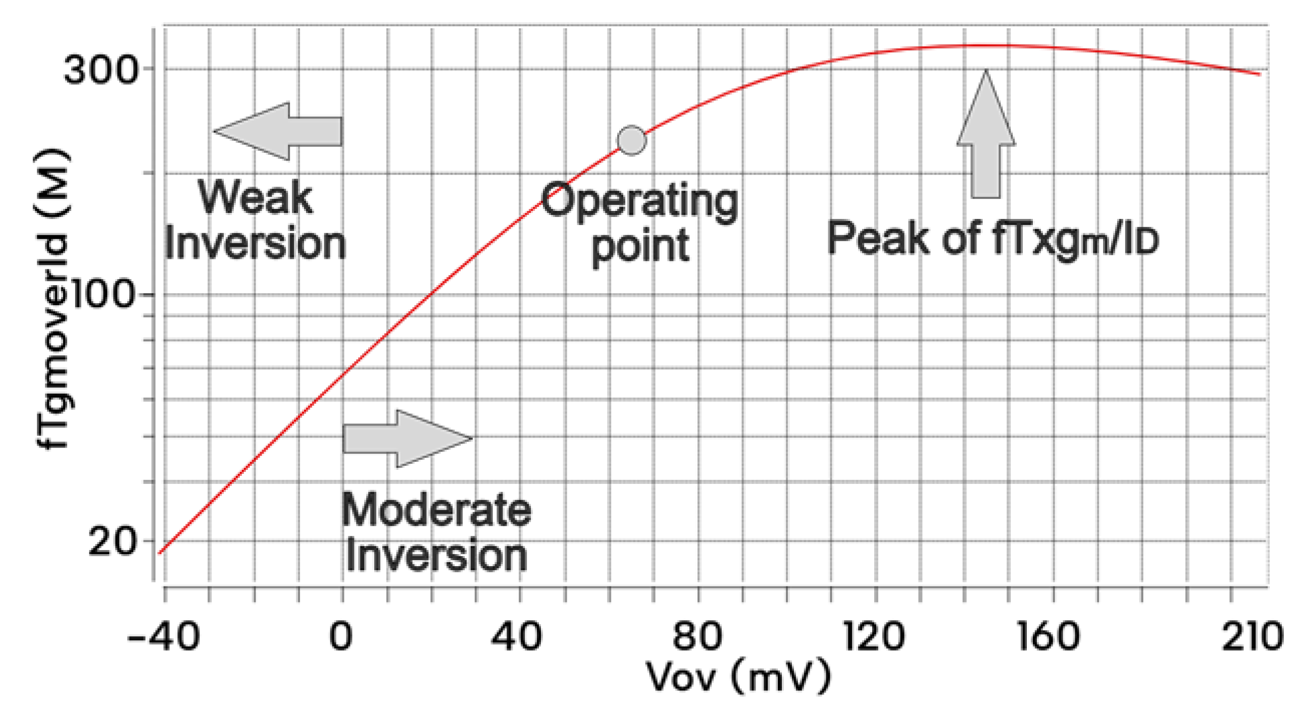
Figure 16.
Design flow for design and optimization of filters.
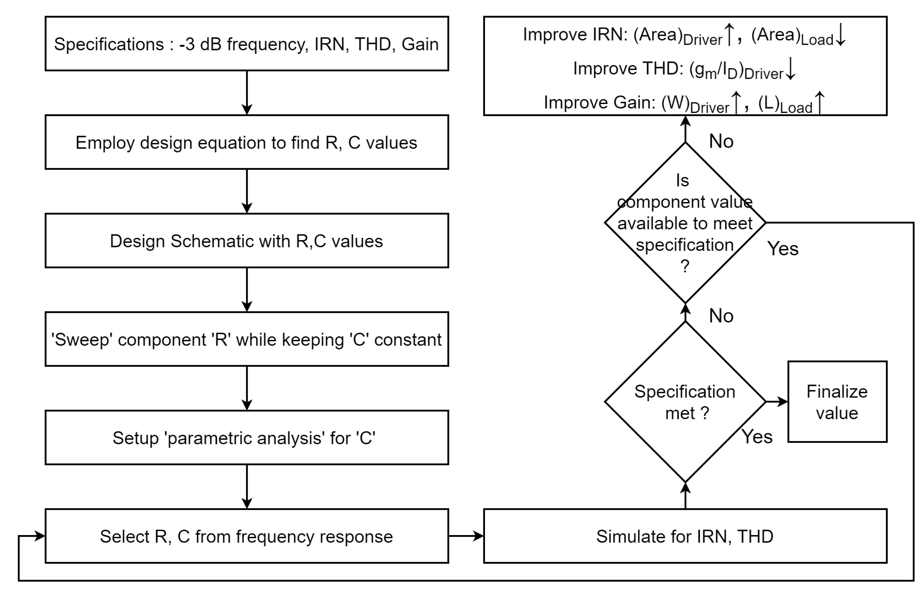
Figure 17.
Proposed ECG acquisition circuit diagram.
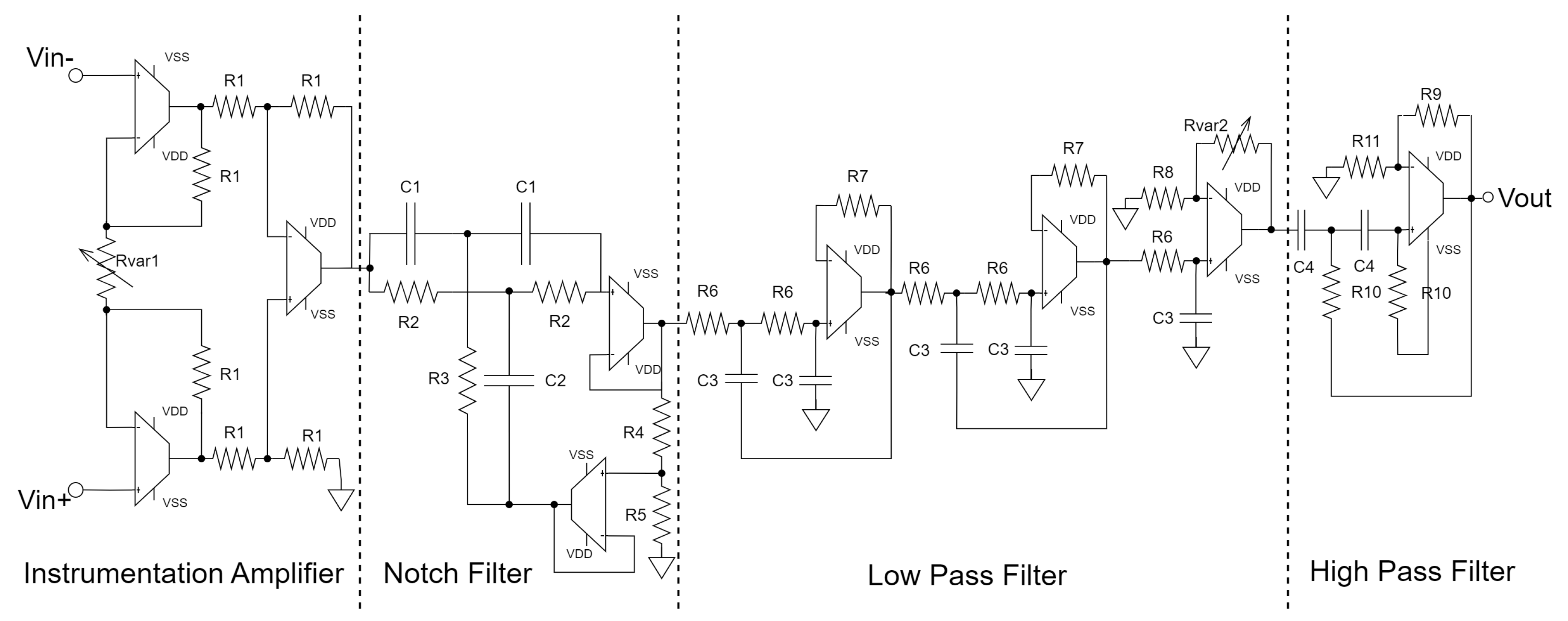
Figure 18.
Test-bench for dc, ac, transient, noise, pole-zero analyses.
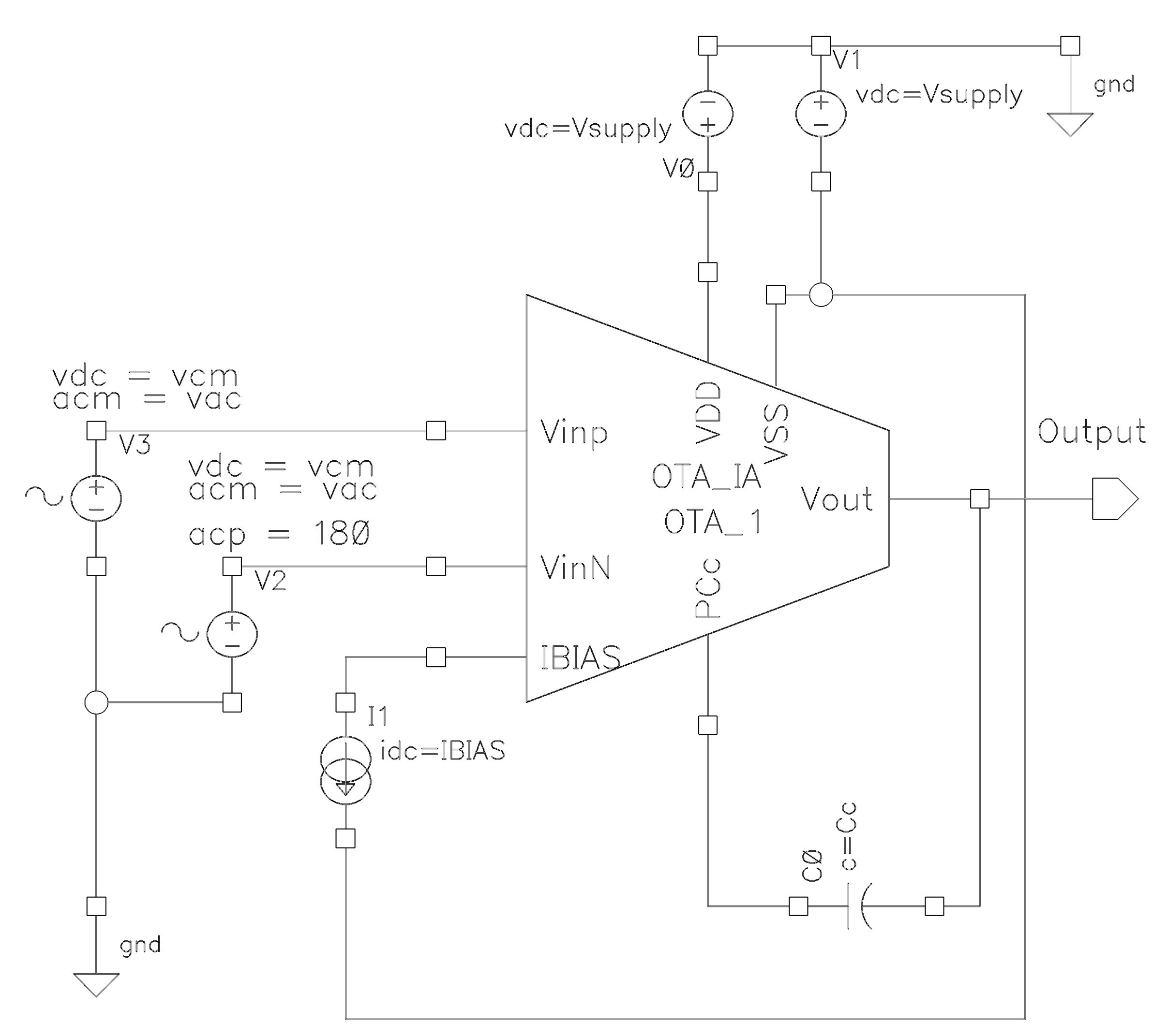
Figure 19.
Magnitude response of the designed OTA.
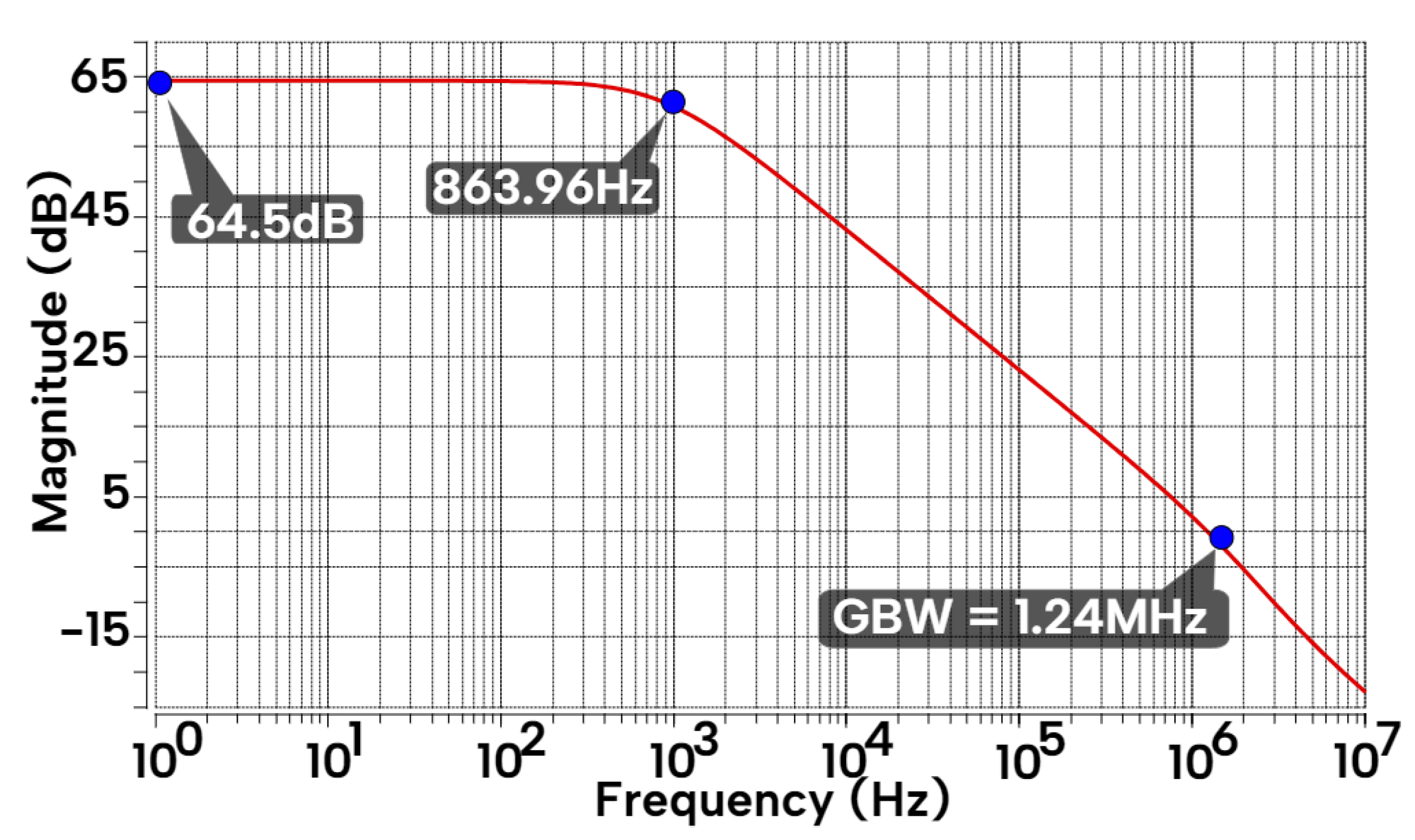
Figure 20.
Pole zero map of the OTA.
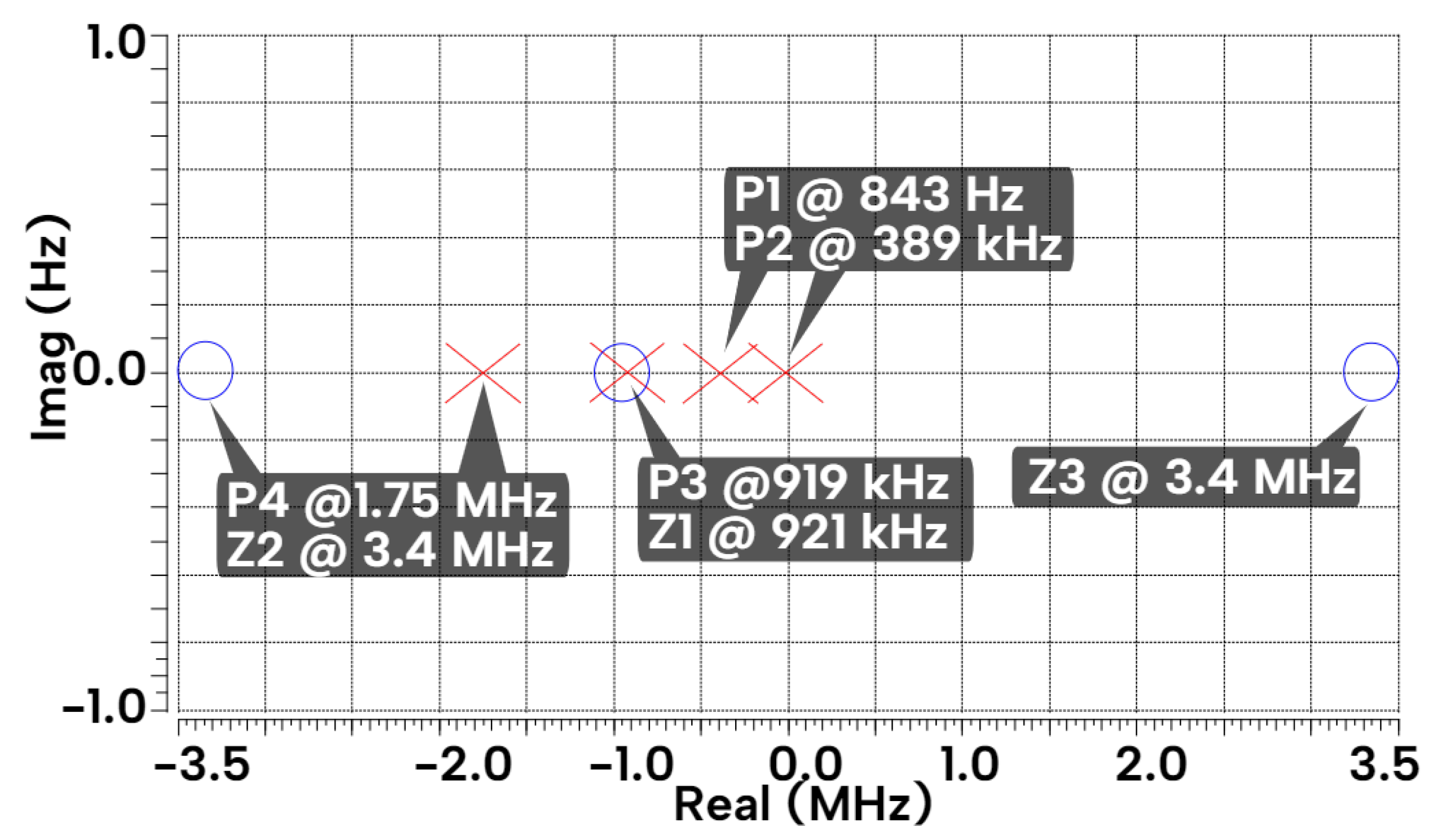
Figure 21.
CMRR waveform vs. frequency.
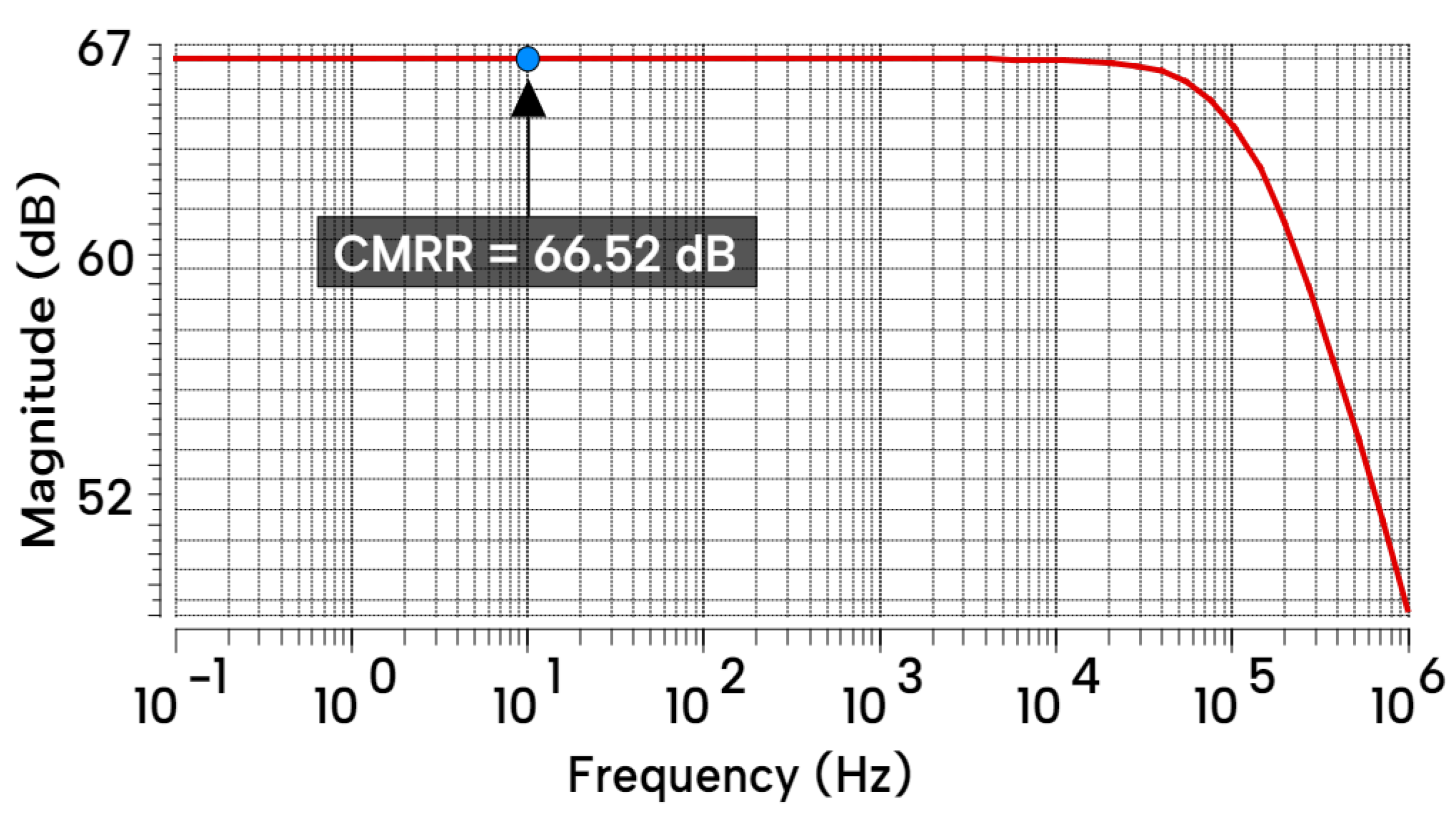
Figure 22.
PSRR waveform vs. frequency.
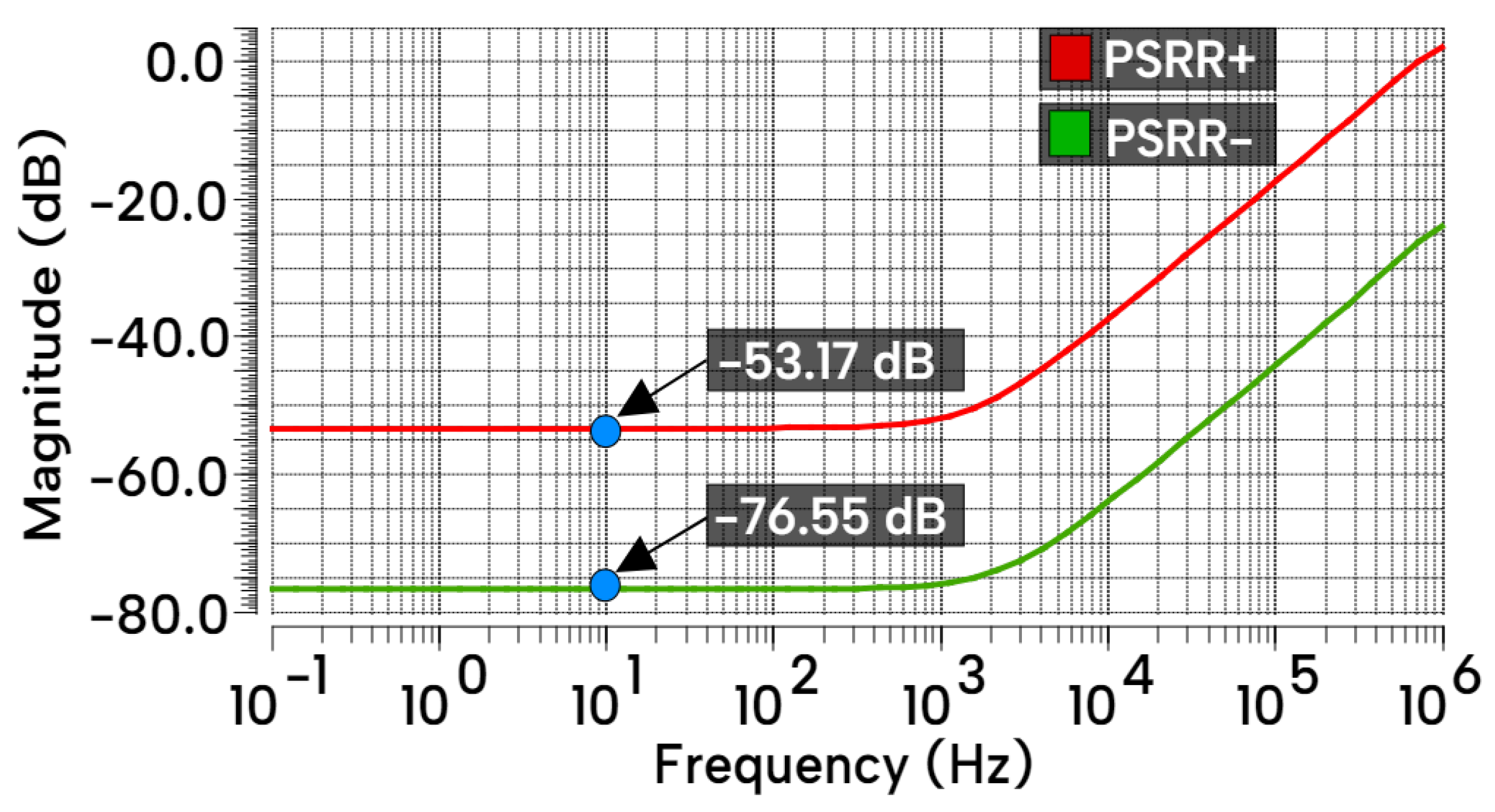
Figure 23.
Output voltage spectrum of the designed OTA for an input sinusoidal of 100 Hz and 0.4 mV p-p.
Figure 23.
Output voltage spectrum of the designed OTA for an input sinusoidal of 100 Hz and 0.4 mV p-p.
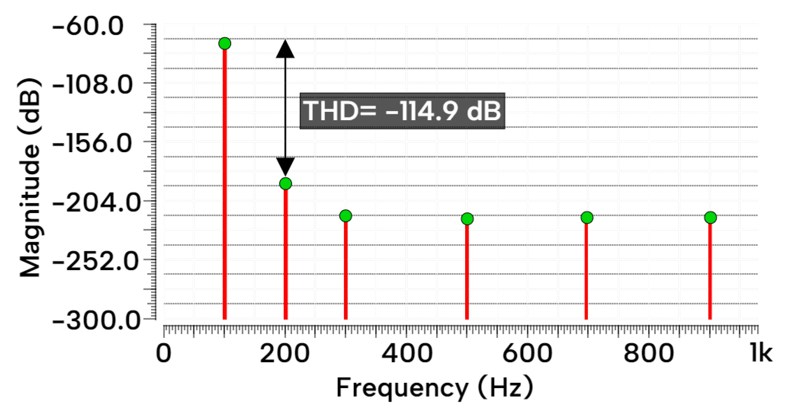
Figure 24.
Output impedance of the Operational Trans-conductance Amplifier.
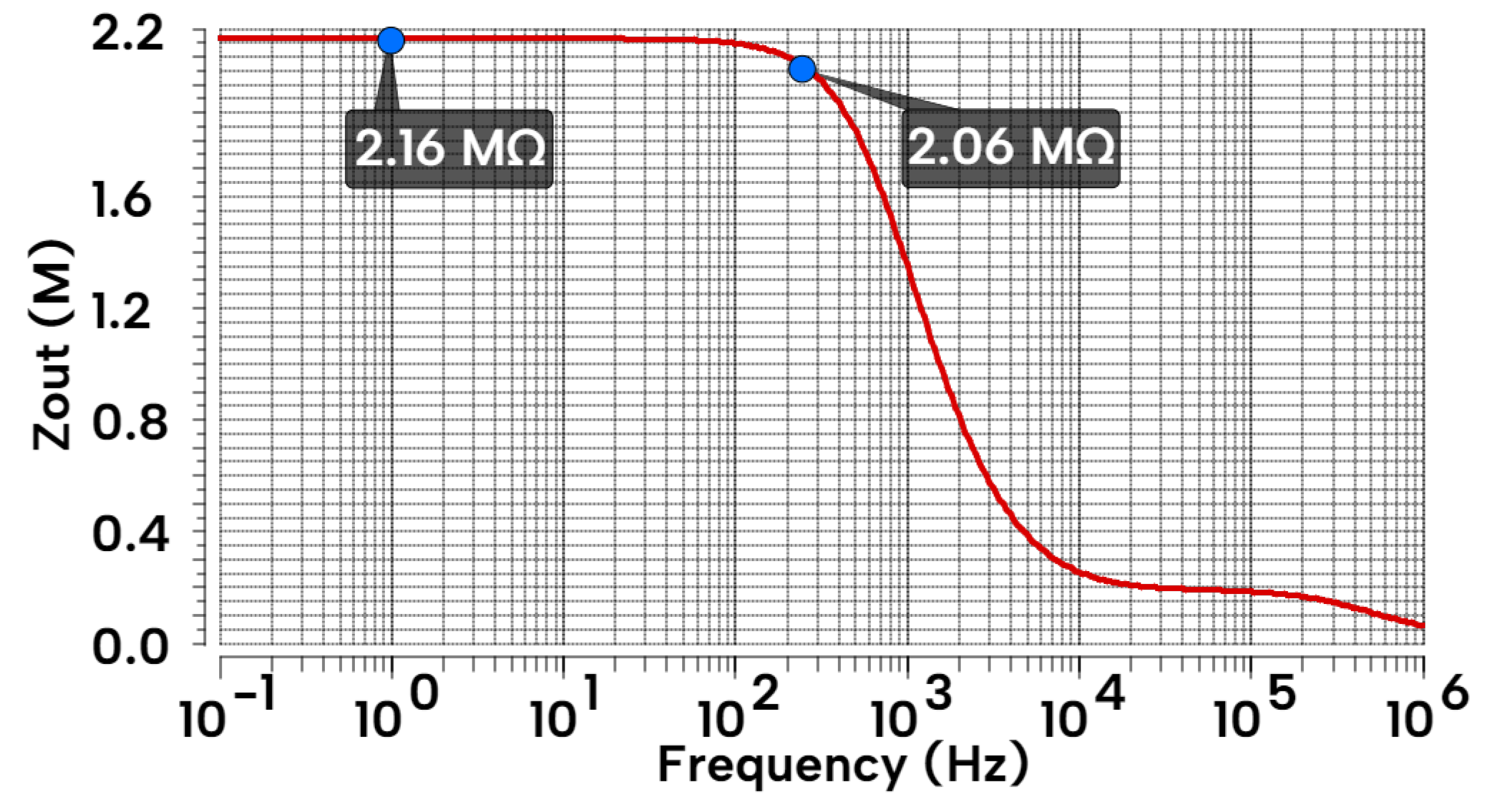
Figure 25.
Input impedance of the Operational Trans-conductance Amplifier.
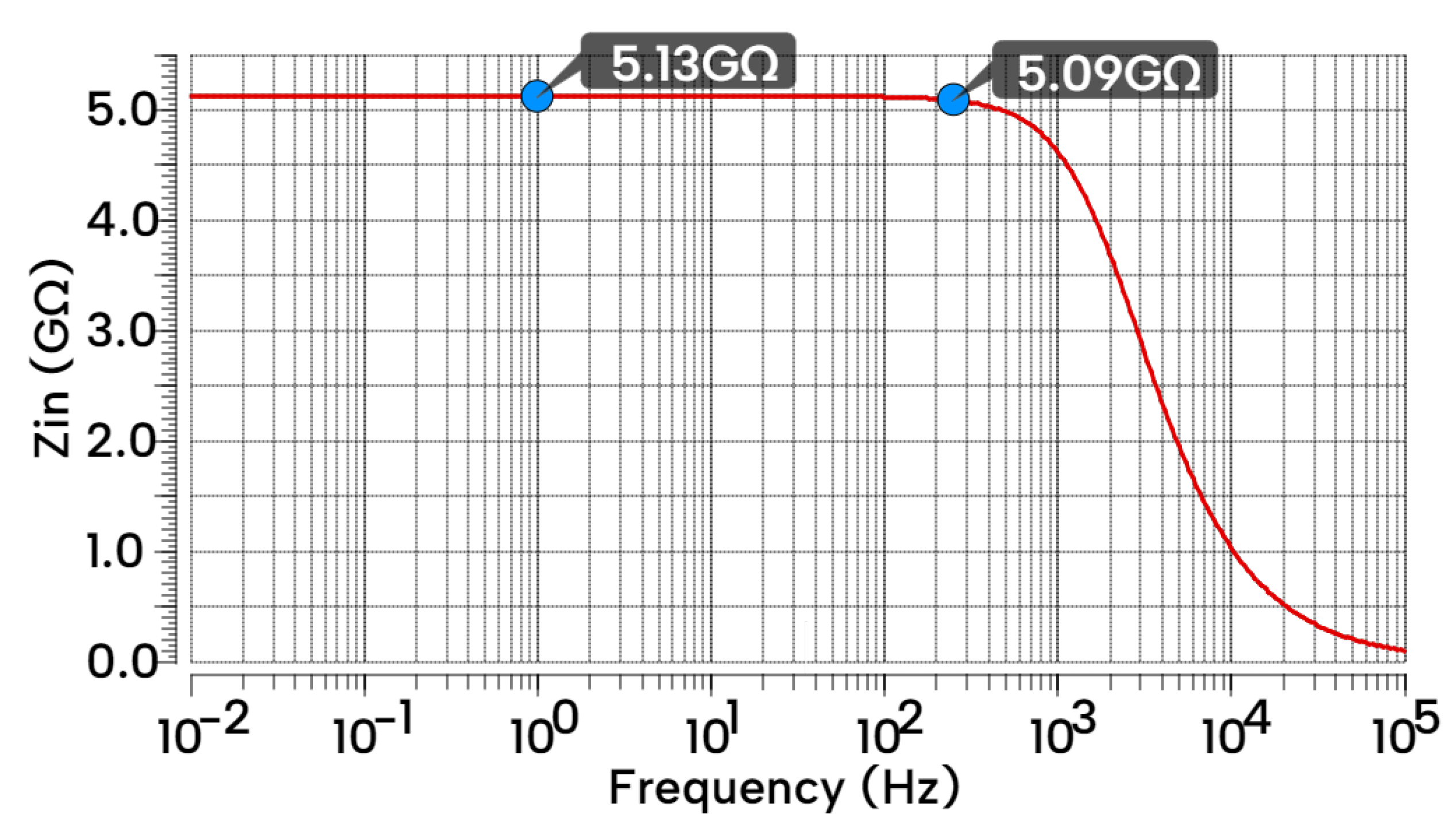
Figure 26.
Threshold voltage deviation distribution
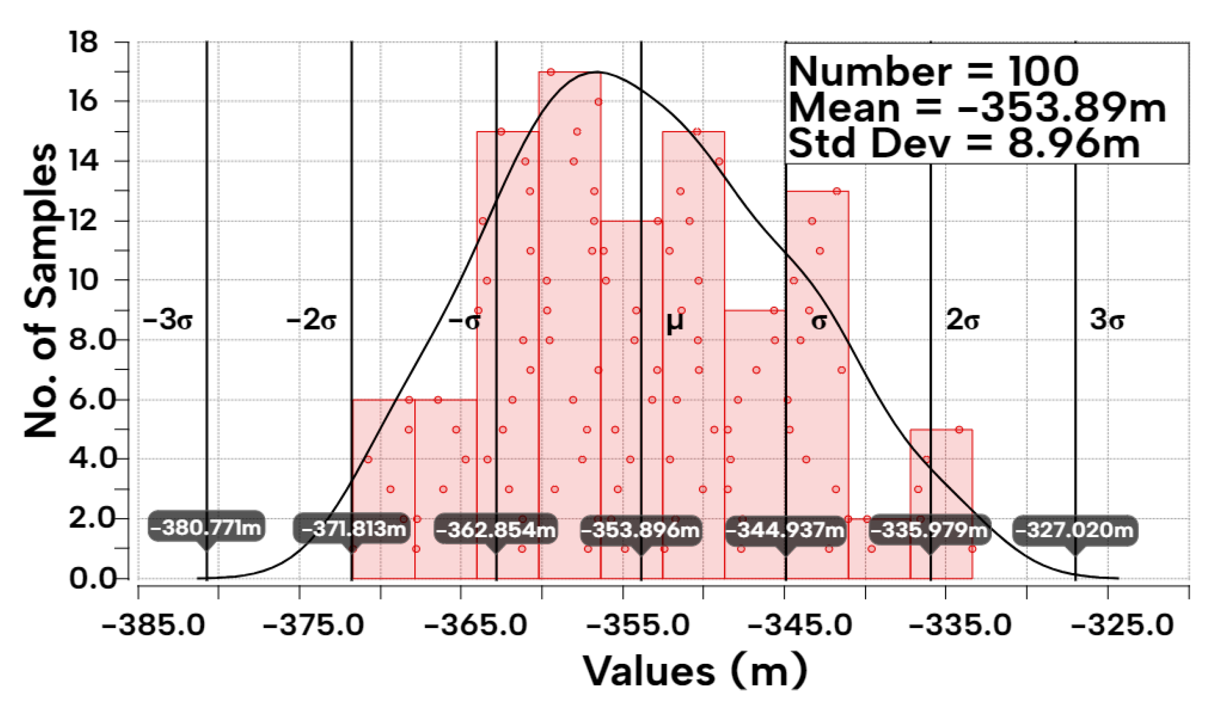
Figure 27.
Test-bench for the final ECG acquisition system.
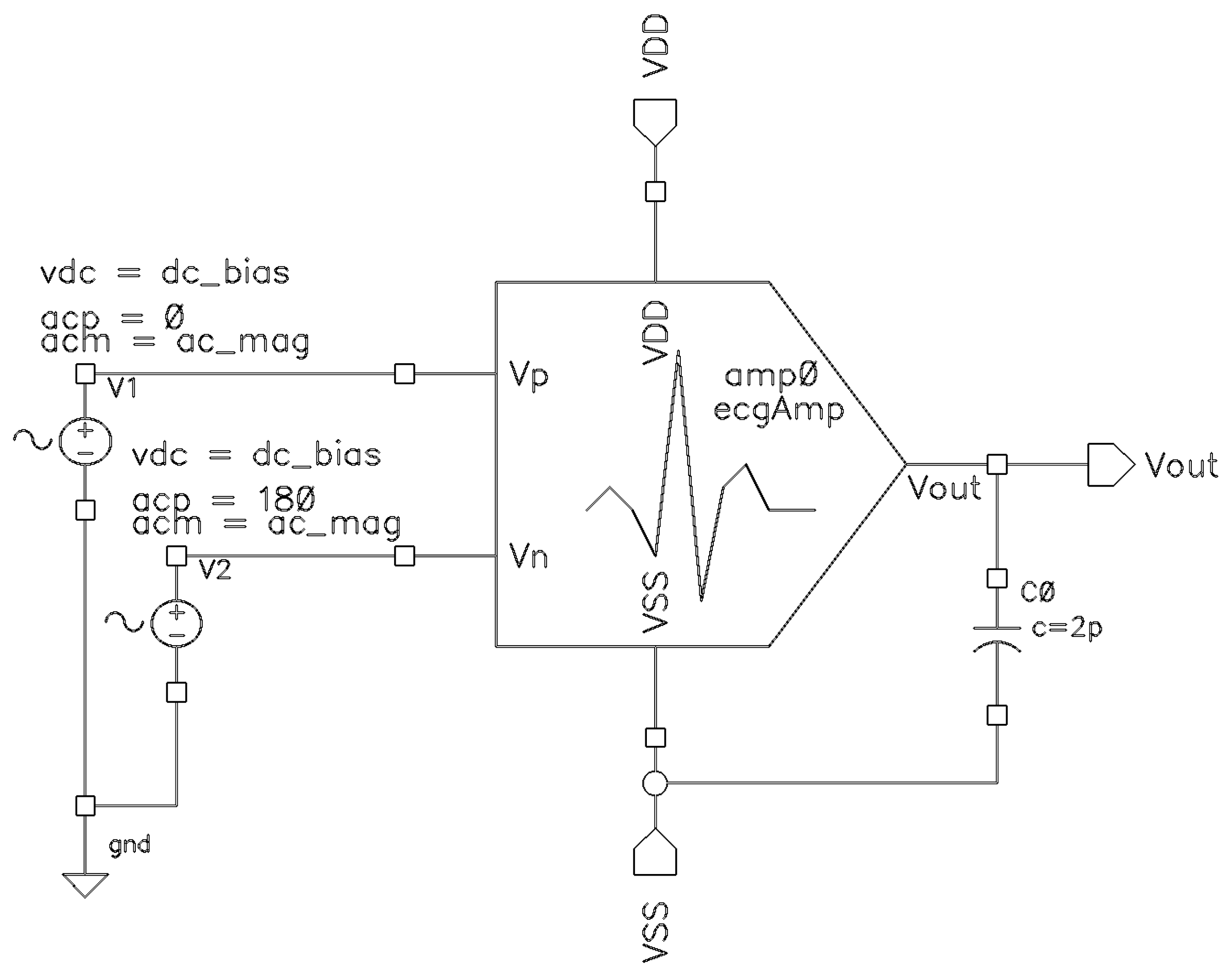
Figure 28.
Magnitude Response of the whole ECG system.
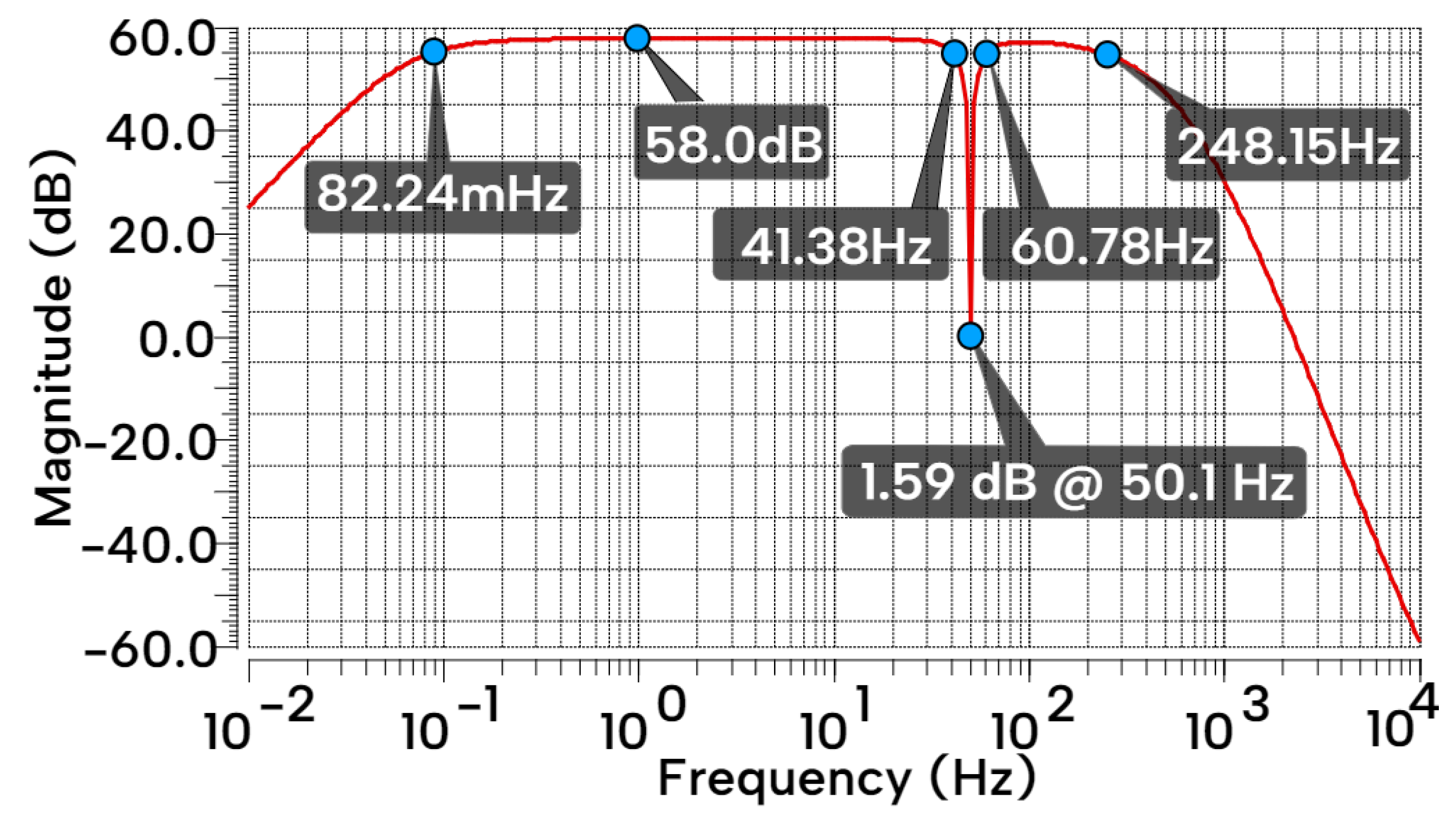
Figure 29.
Pole-zero locations of the ECG system.
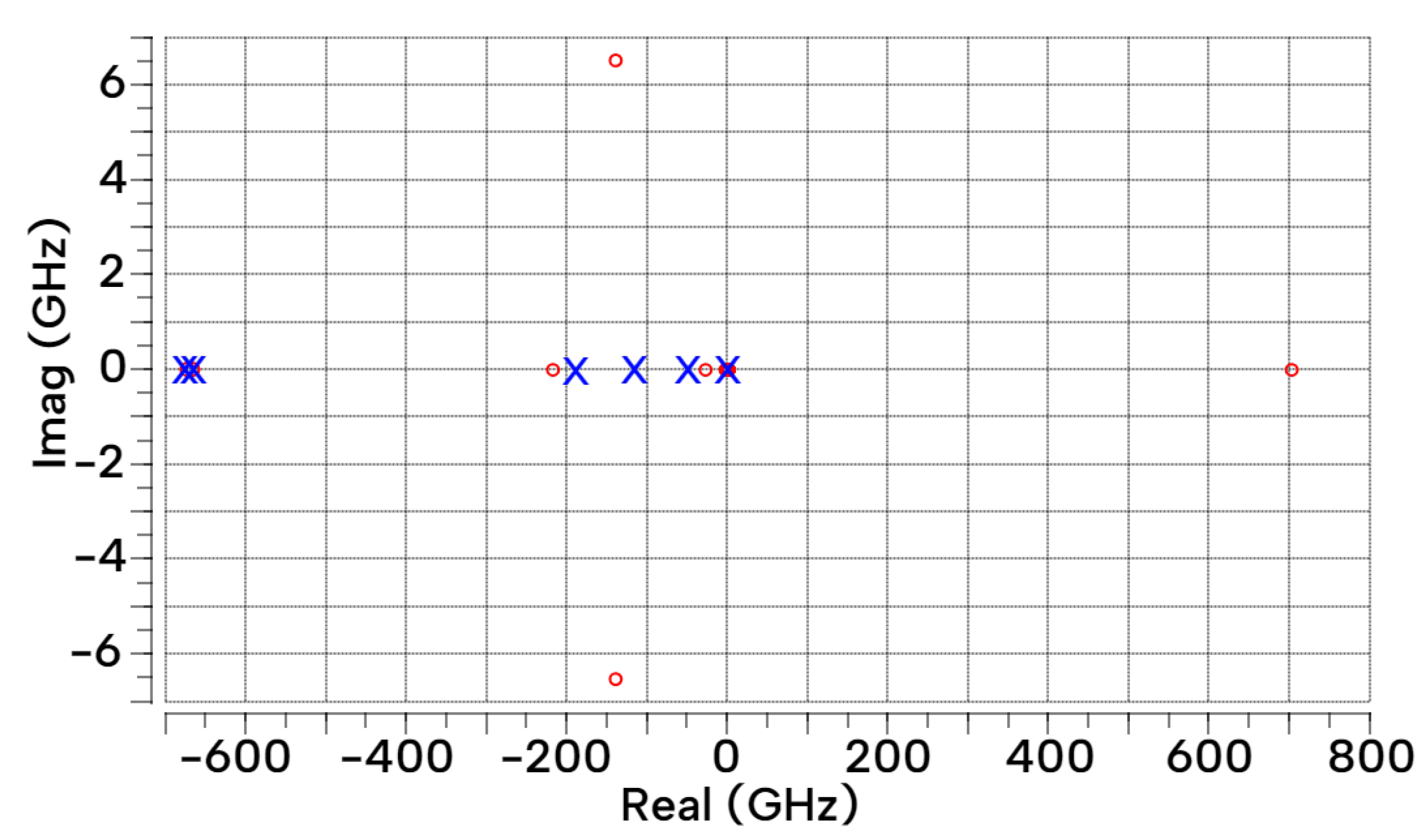
Figure 30.
Input referred noise density.
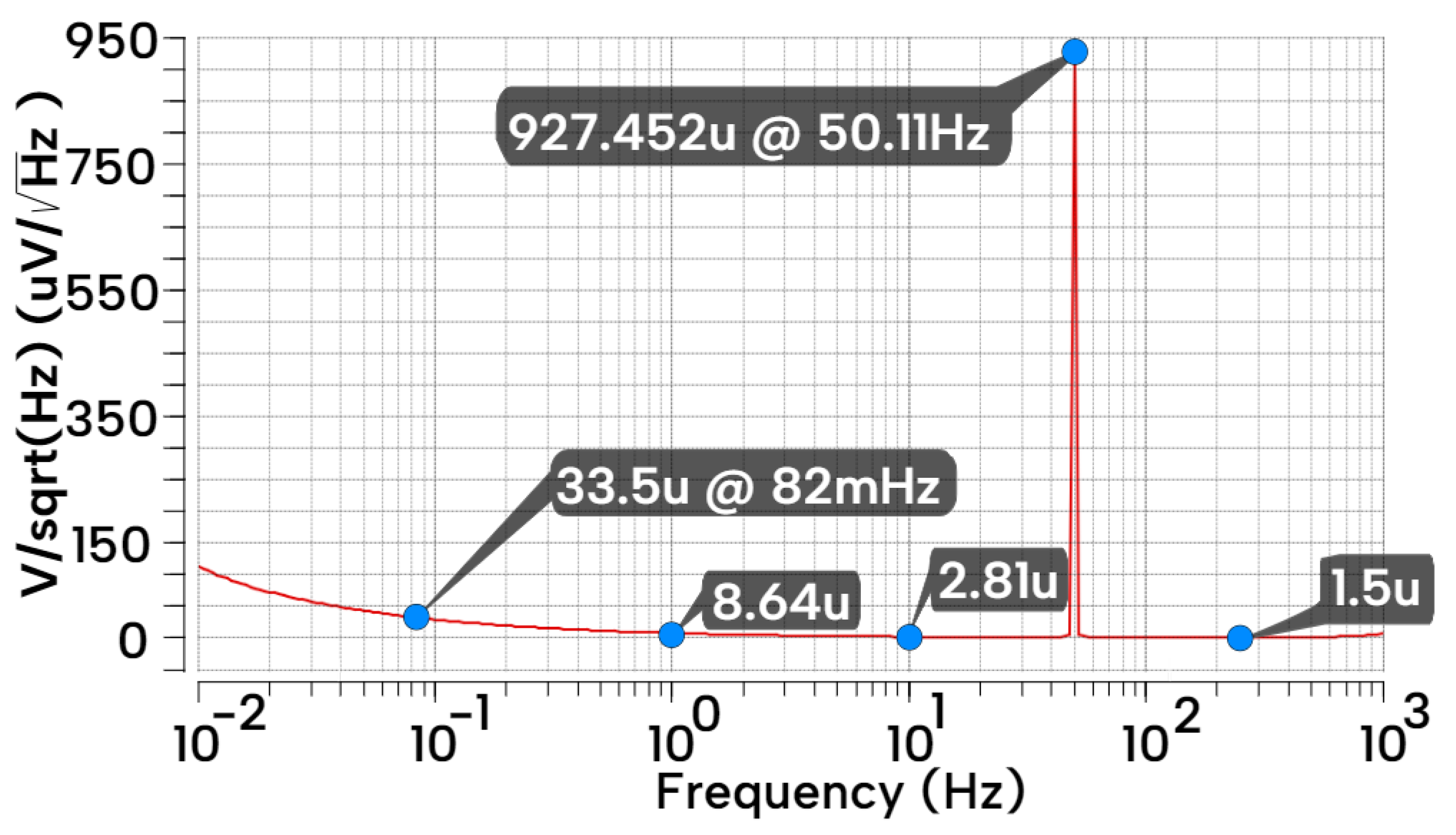
Figure 31.
(Left) ECG spectrum with added noise at 50 Hz and 500 Hz. (Right) Output voltage spectrum of the designed ECG acquisition system.
Figure 31.
(Left) ECG spectrum with added noise at 50 Hz and 500 Hz. (Right) Output voltage spectrum of the designed ECG acquisition system.
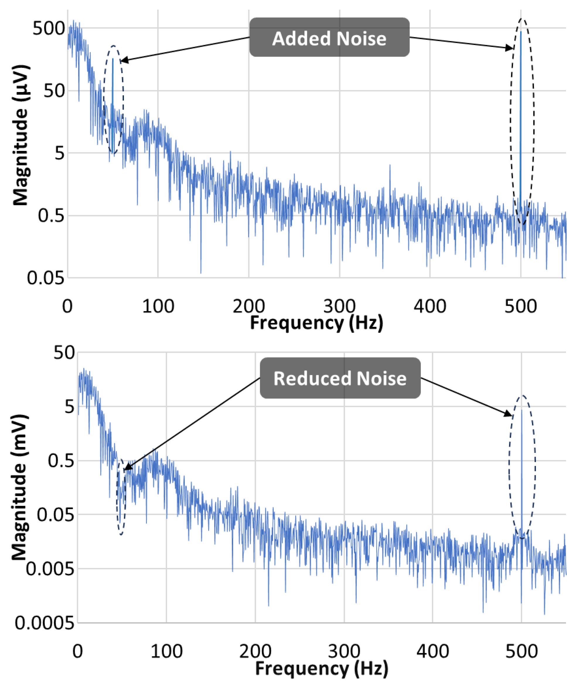
Figure 32.
Output of ECG the system for noisy inputs.
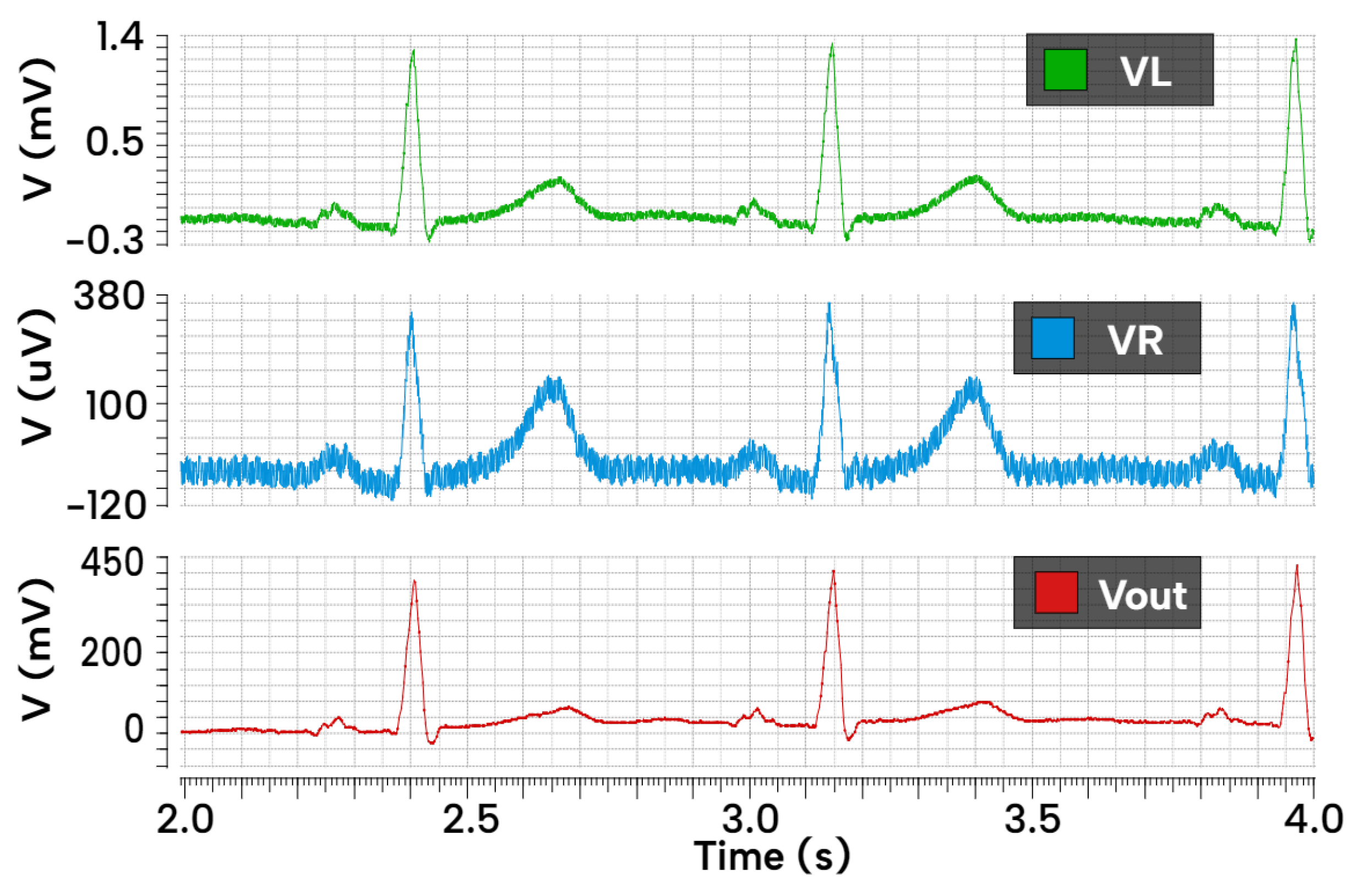
Figure 33.
THD for various amplitude and frequency.
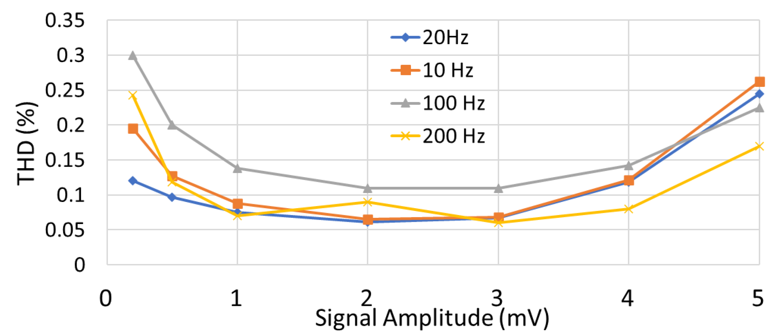
Figure 34.
(Left) Layers used in layout. (Right) Post layout view for the instrumentation amplifier OTA.
Figure 34.
(Left) Layers used in layout. (Right) Post layout view for the instrumentation amplifier OTA.
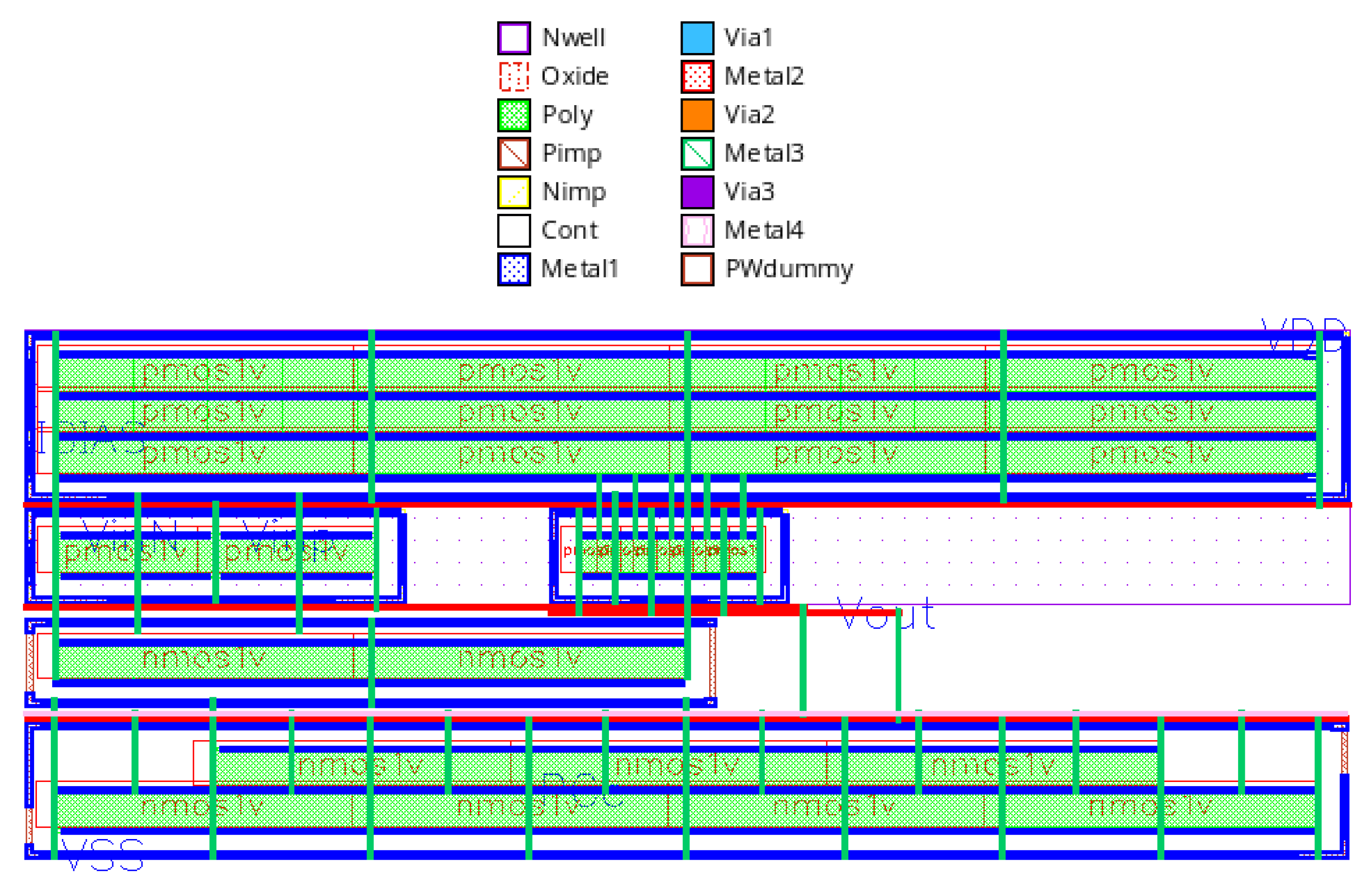
Figure 35.
Post layout magnitude response of the instrumentation amplifier OTA.
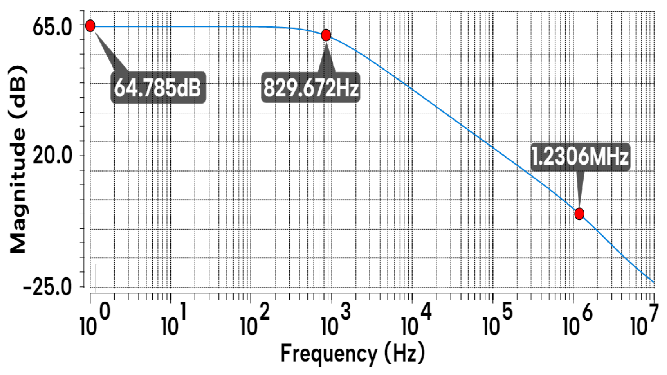
Figure 37.
The proposed ECG acquisition system post layout frequency response.
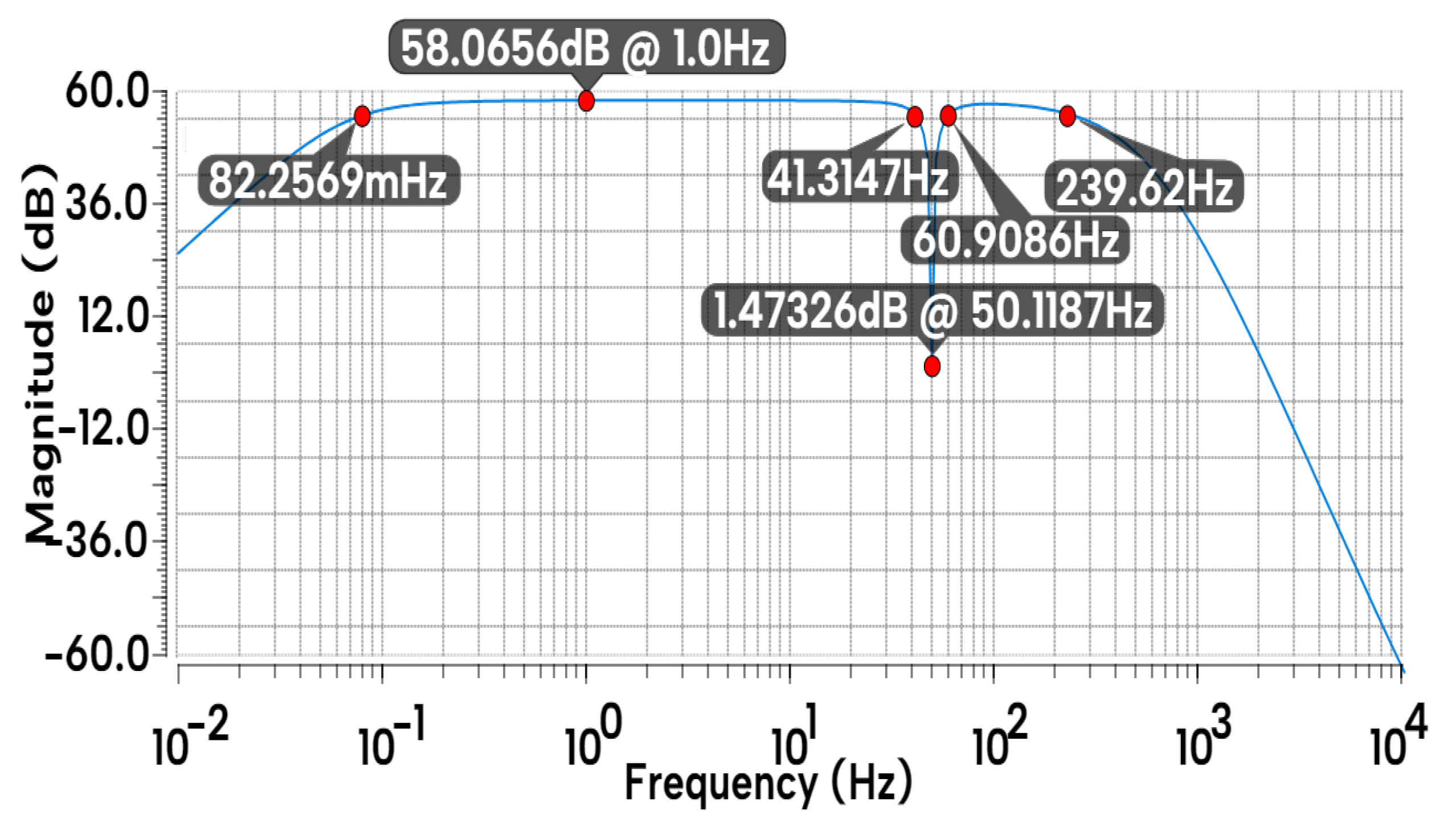
Figure 38.
The proposed ECG acquisition system post layout input referred noise.
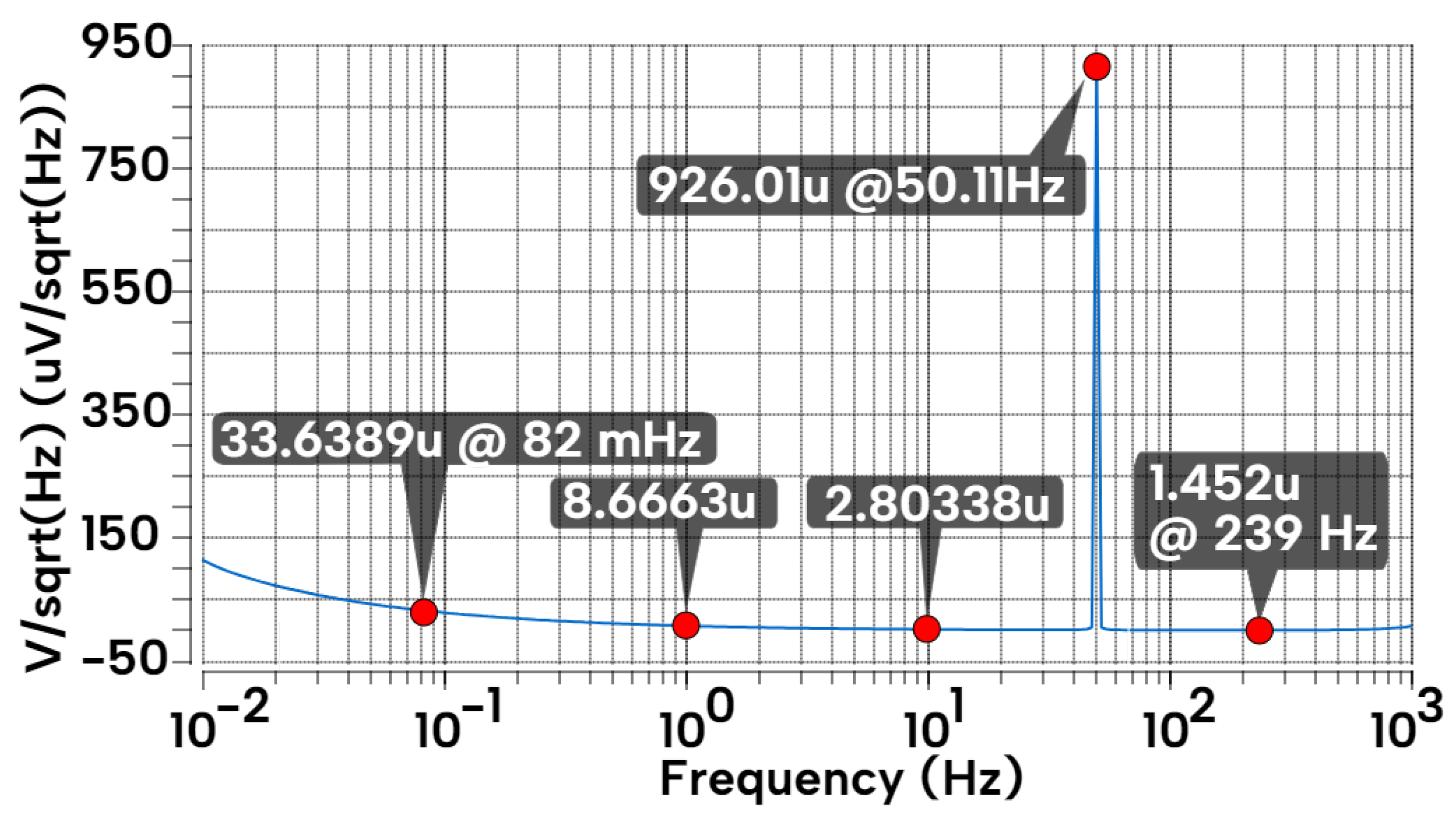

Table 1.
Summary of design requirements for individual MOSFETs of the 2 stage miller compensated OTA.
Table 1.
Summary of design requirements for individual MOSFETs of the 2 stage miller compensated OTA.
| MOSFET | Inversion region | Area | |
|---|---|---|---|
| Moderate | Large | High to Medium | |
| Strong | Small | Low | |
| Strong | Small | Low | |
| Moderate | Large | High to Medium | |
| Strong | Small | Low |
Table 2.
Design specification for the 2 stage miller compensated OTA.
| Parameter | Value |
|---|---|
| ±0.6 V | |
| 200 nA | |
| GBW | 1.25 MHz |
| Slew Rate | 0.67 |
| CMRR | High () |
| PSRR | High () |
| THD | Low () |
| 2 pF |
Table 3.
Summary of dc operating point of each MOSFET device for the first iteration.
| MOSFET | Aspect Ratio (W/L) | |||
|---|---|---|---|---|
| 1/5 | -301.62 mV | 101.38 nA | 23.91 | |
| 1/10 | 386.64 mV | 101.38 nA | 16.96 | |
| 6/10 | -511.73 mV | 203.05 nA | 15.61 | |
| 7/5 | 331.27mV | 573.03 nA | 20.87 | |
| 5/1 | -868.72 mV | 573.03 nA | 16.91 | |
| 6/10 | -424.84 mV | 199.64 nA | 15.73 |
Table 4.
Design parameters for the 2 stage miller compensated OTA of instrumentation amplifier.
| Parameter | Value |
|---|---|
| ±0.6 V | |
| 200 nA | |
| 1 m/5m | |
| 1 m/10 m | |
| 6 m/10 m | |
| 7 m/10 m | |
| 5 m/1 m | |
| 500 fF |
Table 5.
Finalized aspect ratios for the optimized OTAs.
| Parameter | IA | LPF | HPF | Notch |
|---|---|---|---|---|
| 1 m/5m | 2.5m/5m | 1m/10m | 1m/5m | |
| 1 m/10 m | 1m/10m | 1m/10m | 1m/10m | |
| 6 m/10 m | 6m/10m | 6m/10m | 6m/10m | |
| 7 m/10 m | 1m/10m | 1m/5m | 5m/5m | |
| 5 m/1 m | 0.9m/0.9m | 10m/1m | 7m/1m |
Table 6.
Design parameters for the proposed ECG acquisition system.
| Parameter | Value |
|---|---|
| R1 | 300 M |
| R2 | 32 M |
| R3 | 16 M |
| R4 | 10 M |
| R5 | 99 M |
| R6 | 190 M |
| R7 | 400 M |
| R8 | 900 M |
| R9, R10 | 3.5 G |
| R11 | 1 G |
| Rvar1 | 60 M |
| Rvar2 | 200 M |
| C1 | 99.2 pF |
| C2 | 198.4 pF |
| C3 | 1.4 pF |
| C4 | 900 pF |
Table 7.
Performance comparison of the proposed OTA with previously reported work.
| Parameter | This Work | [18] | [19] | [20] |
|---|---|---|---|---|
| Tech [nm] | 45 | 350 | 180 | 180 |
| Topology | Miller-OTA | CR-OTA1 | GBFC-IBL2 | MI-OTA3 |
| Supply [V] | ±0.6 | 2 | ± 0.75 | ± 0.5 |
| [A] | 816n | 160n | 570n | 200n |
| Power [nW] | 980 | 320 | 855 | 267.5 |
| Gain [dB] | 64.5 | 39.8 | 47.6 | 31.17 |
| PSRR [dB] | 76.55 | 70 | - | 37.26 |
| CMRR [dB] | 66.55 | 65 | 105.6 | 90.05 |
| THD [%] | <1 | <1 | <1 | <1 |
| IRN [] | 15.9 | 2.05 | 0.12 (PSD) | 174 |
| Zin [] | 5.1 | - | 0.3 | - |
1CR-OTA = Current Re-used Operational Trans-conductance Amplifier 2GBFC-IBL = Gain-boosted folded-cascode with Impedance Boosting Loop 3MI-OTA = Multiple-Input Operational Trans-conductance Amplifier
Table 8.
Input-Referred Noise, Power Consumption and Total Harmonic Distortion for the filters.
| Parameter | 2nd order HPF | Notch Filter | 5th order LPF |
|---|---|---|---|
| Input-Referred Noise | 70.1Vrms/ | 14Vrms/ @ PB | 130Vrms/ |
| Power Consumption | 2.034 W | 2.67 W | 1.21 W |
| Total Harmonic Distortion | -92.5 dB | -52.1 dB | -112.2 dB |
Table 9.
Performance comparison of the designed ECG acquisition system with contemporary designs.
| Parameters | This Work1 | [57]1 | [20]1 | [58]1 | [59]1 | [60]2 |
|---|---|---|---|---|---|---|
| ]1* Technology [nm] | 45 | 180 | 180 | 180 | 180 | 180 |
| ]3* Supply [V] | ±0.6 | 1.8 | ± 0.25 | 0.5 | 0.5 | 1 |
| ]3* Order | HPF-2nd, LPF-5th | LPF-2nd | BPF-3rd | LPF-4th | BPF-2nd | LPF-5th |
| ]3* Power [] | 10.88 | 19.4 | .161 | 0.003 | 0.0313 | 0.041 |
| ]3* Gain [dB] | 58.06 | 34.5 | 0 | -5.6 | 37.1 | -7 |
| ]1* BW [Hz] | .08-239.6 | 1.7-352 | .1-250 | 200 | 1.5-112 | 250 |
| ]3* IRN [] | 33.6 | 3.47 | 198 | 91.9 | 17.9 | 134 |
| ]3* PLI Removal | Notch | No | Notch | No | No | No |
| ]3* Area [mm2] | 0.0058 (off-chip RC) | 156.25 | 0.0528 (off-chip cap) | 0.074 | 0.167 | 0.24 |
1 Post-layout simulated. 2 Measured.
Disclaimer/Publisher’s Note: The statements, opinions and data contained in all publications are solely those of the individual author(s) and contributor(s) and not of MDPI and/or the editor(s). MDPI and/or the editor(s) disclaim responsibility for any injury to people or property resulting from any ideas, methods, instructions or products referred to in the content. |
© 2024 by the authors. Licensee MDPI, Basel, Switzerland. This article is an open access article distributed under the terms and conditions of the Creative Commons Attribution (CC BY) license (http://creativecommons.org/licenses/by/4.0/).
Copyright: This open access article is published under a Creative Commons CC BY 4.0 license, which permit the free download, distribution, and reuse, provided that the author and preprint are cited in any reuse.


