Submitted:
18 April 2024
Posted:
22 April 2024
You are already at the latest version
Abstract
Micro-Raman spectroscopy was carried out to evaluate the localized residual stresses in commercial Gallium Nitride-based devices, specifically AlGaN/GaN High Electron Mobility Transistors (HEMTs) in a novel packaging design provided by STMicroelectronics S.r.l. The packaging plays a key role in protecting the device core against the external environment, thus minimizing damages caused by mechanical shocks, exposure to light, and contact with chemicals, conjointly achieving an efficient heat dissipation rate. Even though the packaging is a required step for the proper functioning of ready-to-use electronic devices, its application typically may introduce mechanical stress to AlGaN/GaN HEMTs, which can result in various reliability issues. In this paper, we investigate the impact of packaging on residual stress by analyzing the frequency shift of the E2 Raman peak along GaN layers and at the GaN/Si interface. An extensive evaluation was conducted using both a packaged device and a wafer-level device. The correlation between Raman frequency shifts of the E2 mode was accurately quantified, revealing a stress mitigation of approximately 0.1 GPa. This reduction is ascribed to the compressive stress introduced by the packaging, which partially offsets the intrinsic tensile stress of the wafer-level device. The proposed methodology could, in principle, be implemented to improve the development of a packaging.
Keywords:
AlGaN/GaN high electron mobility transistor
; micro-raman spectroscopy
; power electronic
; packaged device
; wafer-level
1. Introduction
Among Wide Bandgap Semiconductors (WBSs), Gallium Nitride (GaN) is emerging as the latest breakthrough in developing novel energy-efficient power electronic devices and optoelectronic components [1]. It is characterized by a crystallographic arrangement typical of wurtzite, where Gallium (Ga) and Nitrogen (N) atoms are spatially arranged to form a superimposed hexagonal packed lattice. Power electronics has recently leveraged the characteristics of wide bandgap materials to overcome the limitations imposed by silicon. In particular, the increasing demand for the next generation of high-efficiency power converters has pushed up the development of devices capable of operating at higher frequencies and temperatures, achieving higher conversion efficiency. Among these devices, GaN-based technology has been employed to develop AlGaN/GaN high electron mobility transistors (HEMTs) [2,3,4]. These devices find applications in electric vehicles, phone chargers, renewable energies, and more, as they meet the above specifications, are able to operate at high temperatures, frequencies, voltages, and currents, and allow the design of systems that occupy less space and generate less heat [5]. However, due to the limited commercial availability of bulk-GaN substrates [6], GaN-based electronics are typically developed using alternative substrates such as sapphire (), Silicon Carbide (SiC), and silicon (Si) [7]. Nevertheless, owing to its cost-effectiveness and availability in large wafer sizes (e.g., 12-inch wafers), silicon (Si) substrate is widely used and predominant compared to SiC and substrates, which are available in smaller-sized wafers (e.g., 6 or 8 inches) [8]. Moreover, silicon technology and fabrication processes are more mature and advanced. Besides, the presence of an AlGaN (Aluminum Gallium Nitride) modulation layer on silicon substrate plays a crucial role in mitigating defects in GaN semiconductor materials. These factors, along with the higher costs associated with SiC, have positioned silicon as the preferred substrate for electronic industrial production. Although silicon is a dominant choice and more commonly used for electronic applications, it’s worth noting that there are specific applications where SiC or sapphire substrates might be preferred, depending on the performance requirements and specific characteristics of the devices being developed.
The packaging of electronic devices plays a critical role in ensuring their functionality, reliability, and protection from external factors (chemicals, light exposure, and mechanical impact) [9], while simultaneously guaranteeing a good connection between the chip and the board. For these reasons, many studies have been conducted to identify the best kind of packaging for the desired applications, testing different designs and materials. More specifically, the electronic device packaging research field has become increasingly active as the demand for power devices has increased [10]. Among all the analyzed factors that can affect both performance and lifetime of a device, the effect of the mechanical stress on the chip surface is rarely taken in account [11]. Due to the lattice reticular mismatch between the AlGaN/GaN HEMT and the chosen substrate, along with the difference in thermal expansion coefficients [12], there is a significant built-in strain/stress capable of modifying the overall performance of GaN-based device. Moreover, regardless of the type of used substrate, AlGaN/GaN HEMTs must be encapsulated within specific packaging, typically made up of metal, glass, plastic, or ceramic materials.
The electronic device studied in this work uses a bond-wire-free package designed around the chip to save space and optimize thermal dissipation. This package comprises a lead frame onto which the die is soldered using a silver sinter paste. Fiberglass is used to plane the intermediate space. Holes are then dug into the glass fiber, onto which copper is deposited, and subsequently etched down using a dedicated mask, leaving the final connection. Despite its utility, the packaging encapsulation process may induce unwanted additional mechanical residual stresses across various layers of the device and at the die/packaging interface. The additional mechanical stress can be even more burdensome under normal operating conditions due to differences in thermal expansion coefficients between the various materials composing the device [13]. The above results in a continuous stream of reliability challenges in the field of advanced packaging technology. This work focus on the effect of packaging on the stress among the semiconductor layers constituting the device. In particular, the thermal mismatch contributes to premature device failure through a variety of mechanisms, including packaging, die, wire, and solder bump crack, as well as delamination. In this context, Micro-Raman spectroscopy emerges as a potent non-contact, local, and non-destructive molecular characterization technique [14] capable to assess localized residual strain/stress across the entire thickness of the AlGaN/GaN HEMT [15], with a sub-micron lateral resolution. Significantly, when crystals are subjected to mechanical stress, the frequency of their characteristic Raman modes shifts due to stress-induced crystal deformations [9]. The GaN crystal Raman spectrum can be populated by eight different optical modes, four of which are Raman active in our geometry, namely A1(TO), E1(TO), E2(low), and E2(high) [16]. Among the detectable phonon modes, the E2(high), which arises from atomic oscillations along the c-plane, turns out to be more susceptible to lattice strain elongations, constituting a good marker for the quantification of residual stresses in AlGaN/GaN HEMT devices [17]. According to the previous consideration, the frequency-center (ω) of the E2 (high) mode was monitored along a vertical direction spanning from the bottom to the top of the HEMT devices crossing the entire AlGaN/GaN heterostructures. This comprehensive analysis was conducted for both AlGaN/GaN HEMT-PD and AlGaN/GaN HEMT-B samples. This approach, together with using specific strain/stress relation, enables to correlate the optical data, as achieved by micro-Raman spectroscopy, and the residual stress existing within the layers of the device under test [1,7,18,19]. Knowledge of the aforementioned aspects not only helps to evaluate the performance of GaN-based electronics for various applications, but also provides valuable information for the understanding of unknown failure mechanisms which compromise their lifetime.
2. Materials and Methods
2.1. Material
In this study, we explore the impact of packaging on local stress through a comparative analysis of the Raman spectral characteristics between the Packaged Device (PD) AlGaN/GaN HEMT and its unpackaged counterpart, the Bare (B) AlGaN/GaN HEMT, both provided by STMicroelectronics S.r.l. Figure 1 displays images of both the bare AlGaN/GaN HEMT (a) and its packaged counterpart (b).
AlGaN/GaN HEMTs are manufactured by STMicroelectronics S.r.l. by means of Metal-Organic Chemical Vapor Deposition (MOCVD). The process began with the growth of a 5 µm thick GaN(0001) layer on an n-Si(111) substrate, followed by a 16 nm barrier. Afterwards, a p-GaN capping layer has been addicted on the gate region and then, the metallic contacts have been deposited. Subsequently, a passivation layer was deposited to ensure electrical isolation for the AlGaN/GaN high-electron-mobility transistors and, ultimately, packaging. Figure 2 illustrates a cross-sectional view of the AlGaN/GaN HEMT structure.
As displayed in Figure 2, the GaN layer can be split in two layers. The first one, with a thickness of roughly 2 µm, acts as a strain modulation layer at the GaN/Si interface, minimizing the lattice mismatch between the two semiconductors. In this way, the GaN epitaxial layer, will experience a lower built-in mechanical stress. The employment of the p-GaN cap gate and the equilibrium between the aluminum molar fraction and the thickness of the AlGaN layer achieve a normally-off HEMTs with a reasonable positive threshold voltage [20]. Moreover, the two-dimensional electron gas (2-DEG) sheet at the GaN epitaxy/AlGaN interface results in efficient charge depletion processes.
To acquire the Raman spectra of the device layers, it was necessary to cut it transversely. However, a simple cut and subsequent polishing were not the suitable experimental strategies, because they would induce mechanical stress leading to inaccurate measurements. For this reason, ion beam milling technique was employed, as it avoids external compressions or deformations phenomena. In this context, two identical devices were prepared, one of which was at wafer level (HEMT-B) while the second was encapsulated (HEMT-PD). The purpose was to analyze their Raman spectra and highlight the impact of encapsulation on residual stress.
2.2. Method
Micro-Raman spectra were collected along the cross-sections of both HEMT-B and HEMT-PD samples to assess the spectral changes induced by the residual stress [21] across the layers of the devices under test. Measurements were carried out at room temperature (RT) using a NT-MDT NTEGRA Spectra confocal micro-Raman working in reflection mode. A solid-state linear polarized DPSS laser operating at 532 nm (Nd:YAG laser), was employed as excitation source limiting the maximum power to ~ 400 µW to prevent any displacement of the Stokes peak induced by temperature increases [22]. An IDUS-type Andor CCD camera cooled with a triple Peltier stage was used as detector. For the purpose of this study, we investigated the spectral range between 500 and 600 with a resolution well below 1 . A 100X objective with a working distance of 6 mm and a numerical aperture of 0.75 was used to focalize the laser beam on the surface of the sample with a spot size of ~350 nm. All measurements were carried out in backscattering geometry, using the microscope objective to capture the scattered light. The samples were positioned with their cross-section facing upwards, taking advantage of a homemade sample holder set-up as depicted in Figure 3. In our experiment, the spring exerts no force on the device and it only keeps the sample in its position. For each sample, 128 micro-Raman spectra were collected along the direction orthogonal to the layers growth with a step size of 78nm, hence covering a 10µm path and crossing through GaN heterostructure (see Figure 2). Each spectrum was acquired with an exposure time of 30 seconds and the entire collection process took 64 minutes.
3. Results and Discussion
Figure 4a shows an optical microphotograph of the cross-section of the sample on which the study was conducted. In particular, the 128 spectra were acquired along the red line crossing the figure orthogonally to the layers. Figure 4b shows the 1D map of the Raman spectra acquired during the experiment along the 10 μm investigated (i.e., the Raman intensities acquired point by point plotted against the Raman shift).
It can roughly be commented that the spectral structures shift when moving from silicon through the layers of GaN, indicating the presence of intrinsic stress. In particular, the GaN Raman peaks in the lower part of the map start to redshift as the position of the area under analysis approaches to the GaN/Si interface. The frequency center of Raman peaks is intimately correlated to the interatomic potential between atoms [23]. Accordingly, changes in this potential due to intrinsic stress within the crystal, lead to Raman shifts of specific and characteristic vibrational modes of the structure, regardless of its origin [23].
Figure 5 displays typical micro-Raman spectra acquired at the GaN epitaxy layer (Figure 5a) and at the GaN/Si interface (Figure 5b). The micro-Raman profile collected at the GaN epitaxy layer (Figure 5a) reveals distinct contributions at 531.7 , 558.7 , and 567.7 respectively associated to the A1(TO), E1(TO) and E2(high) modes of the hexagonal structure of wurtzite. At the GaN/Si interface (Figure 5b), as expected, a characteristic Si Raman peak centered at 521.4 , arising from the Si substrate, is clearly distinguished. Furthermore, the Raman mode deriving from GaN structures, E2(high) at 569.6 , is also observed.
The observed frequency shift of the E2(high) mode, occurring from the GaN epitaxy layer to the GaN/Si interface, can be attributed to the different stress conditions in these two regions.
Since the main purpose of the work is to identify the presence of stress among the layers using Raman spectroscopy, it needs to measure the Raman peak positions with the utmost precision. Despite the rather high spectral resolution of the measurement instrument, obtaining accurate information requires fitting the experimental data using an appropriate model. In particular, the used model consists of 3 Lorentzian lines describing the Raman modes of GaN (A1(TO), E1(TO) and E2(high)), and also takes into account the presence of silicon when it needs. All the 128 spectra were fitted using the model described above to obtain the characteristic frequency ω of the modes point by point along the scanned line. Notably, E2(high) mode was found to be particularly sensitive to biaxial stresses compared to both A1(TO) and E1(TO) modes. For this reason and in agreement with literature, it was used as a marker for quantifying residual stresses [24]. This may be reasonably due to the nature of the E2(high) mode, characterized by atomic oscillations almost perpendicular to the c-axis of wurtzite, hence more sensitive to stress along the chosen axis (see Figure 2).
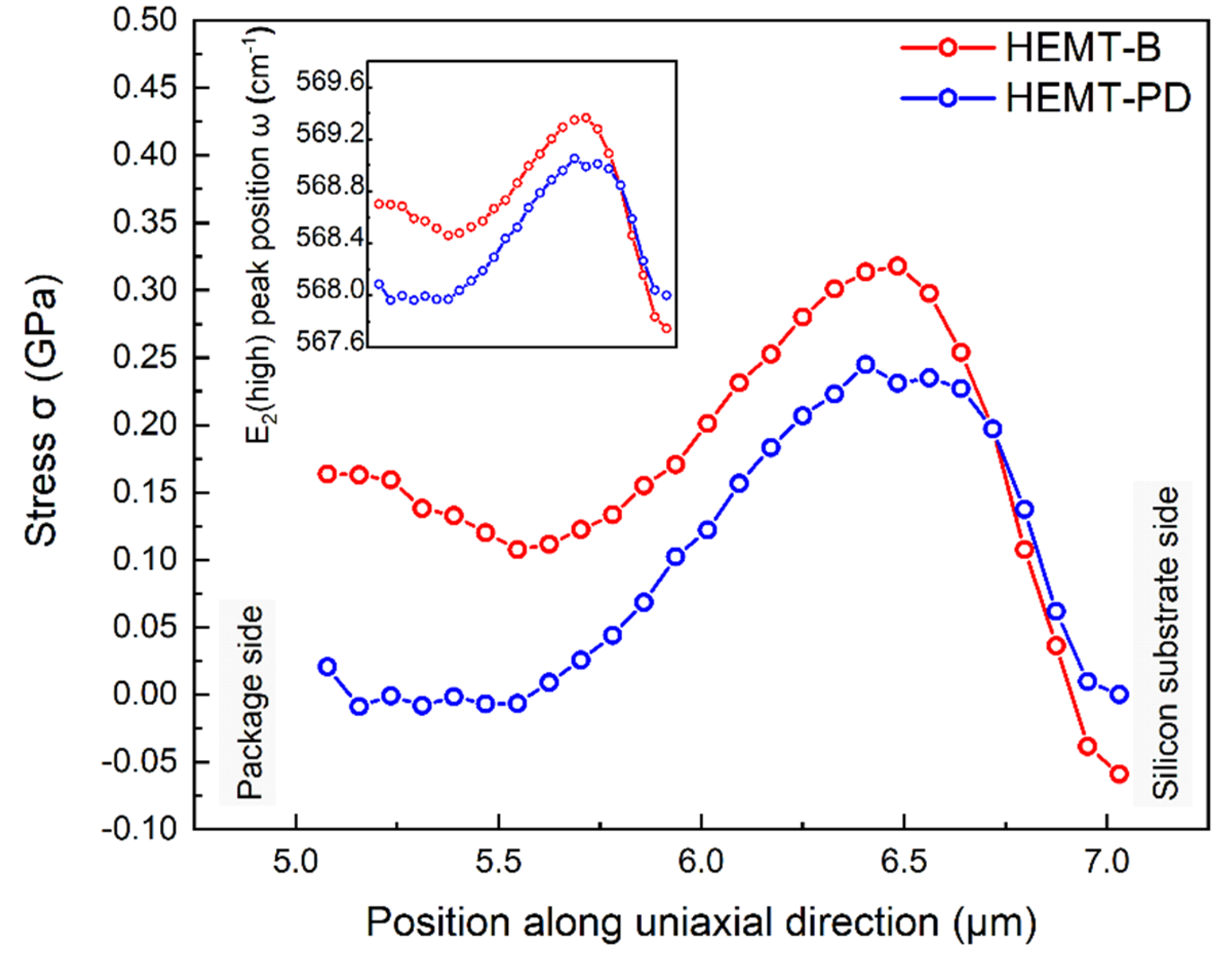
The inset of Figure 6 shows the trend of the frequency of mode E2(high) in the sample HEMT-B (red line) and HEMT-PD (blue line) when moving along the vertical path represented by the red line in Figure 4, i.e., crossing the Al-GaN/GaN heterostructure starting from the package side and moving towards the silicon substrate.
The E2(high) ω values allow calculating the residual stress point by point within the AlGaN/GaN HEMT devices. Indeed, the frequency shift (Δω) linearly depends on the residual stress (σ) according to the relationship:
where K represents the stress coefficient, equal to 4.3 /GPa for GaN grown on c-direction silicon [25]. The frequency shift, Δω, is defined as Δω = ω – ω0, where ω is the peak frequency-center, and ω0 accounts for the corresponding stress-free E2(high) peak frequency-center, fixed at 568 [26]. Figure 6 shows the residual stress σ in GPa, inferred from the frequency shift E2 (high) Δω, as a function of position along the studied path for both HEMT-B devices (red line) and HEMT-PD devices (blue line).
Due to the linear correlation between stress and frequency shift, the E2(high) mode frequency center follows a pattern mirroring that of the stress, as can be deduced by observing the inset of Figure 6. Analyzing the residual stress trend along the AlGaN/GaN HEMT structure (Figure 6), it is worth of note that the influence of the package is mainly visible in the range from 5 µm to 6 µm (zone of interest). In the range between 6.55 µm and 7 µm, the lattice mismatch at the GaN/Si interface induces a more pronounced tensile stress compared to that generated by the presence of packaging, as highlighted by the redshift (a shift towards lower frequencies) of the E2 (high) mode. Furthermore, the non-monotonic behavior observed can be attributed to both the characteristics of the multilayer structure and/or the doping of the layer composing the device. The behavior of E2 (high) in HEMT-B (red curve in the graph shown in Figure 6) shows a slight initial shift towards lower frequency values as it moves through the layers from 5 µm to ~5.5 µm, indicating the presence of tensile stress. This is followed by a clear shift towards the blue in E2 (high), attributed to compression stress likely induced by additional forces or applied loads. Subsequently, near the silicon substrate, a noticeable tensile stress is observed characterized by a frequency shift towards lower frequencies, probably stemming from the lattice mismatch between GaN and silicon. The behavior of the E2 mode in the HEMT-PD device is entirely similar. However, the observed stress values are generally lower across the entire device (blue curve in the graph shown in Figure 6).
The influence of packaging is evident only within the specified area of interest (from 5 to 6.55 µm) located near the surface of the device. Within this region, the packaged device (HEMT-PD) shows a decrease in stress levels of about 0.1 GPa compared to the bare one (HEMT-B). This stress mitigation is attributed to the compression introduced by the packaging, which compensates for the intrinsic tensile stress present between the layers of the device. This result stems from a proper choice of material and packaging design, which must be optimized in terms of shape, dimensions, and thermal properties. Additionally, the incorporation of intermediate layers or buffer materials with more similar thermal properties contributes to reducing stress at interfaces between different materials and ensures effective stress mitigation across the mold.
The mitigation of stress among the active layers of the device has a direct impact on its reliability and performance. Indeed, thermal-mechanical stresses and deformations are already well-known and extensively studied failure mechanisms. In general, lower stress leads to slower aging of the device. Furthermore, when current flows through a device, it undergoes thermal expansion proportional to the current itself due to the increase in temperature in the active region of the device [11]. Generally, this deformation is not uniform across the entire device but depends on the shape and arrangement of the semiconductor part through which the current flows. Particularly, in power switching applications, current values can be very high, resulting in intense heat release and consequent mechanical deformation. Since the crystal can withstand defined stress values beyond which it breaks, it is evident that the presence of residual stress when the device is off can limit the maximum current that can flow through the device without destroying it. This aspect, along with more specifically thermal aspects, must be taken into account when defining the mission profile. Considering the above, it is evident that residual stress mitigation is, among all other advantages, a way to improve the device’s performance and increase its lifetime. Therefore, we can conclude that proper packaging design can effectively enhance the quality and overall reliability of the devices.
4. Conclusions
In this article, micro-Raman spectroscopy was successfully employed to assess the stress/deformation induced by packaging in AlGaN/GaN high-electron-mobility transistors (HEMTs) supplied by STMicroelectronics S.r.l. To evaluate the packaging’s impact, we acquired 128 micro-Raman spectra by vertically scanning along the AlGaN/GaN heterostructure of the device. The data were analyzed using a fitting procedure employing a model consisting of three or four Lorentzians to accurately measure the frequency shift of the phonon modes’ center. Attention was focused on the E2 (high) phonon mode, which is highly sensitive to crystalline stress and therefore can be effectively used for its quantification. Two GaN devices supplied by STMicroelectronics S.r.l were studied, one packaged and the other bare, to assess the influence of packaging on the residual stress present among the active layers of the device.
In the HEMT-PD device, a blue shift of the E2 (high) mode near the packaging was observed, while a slight red shift followed by a blue shift was observed for the bare device. A linear correlation between the Raman frequency shift Δω and stress σ was used to evaluate the compression stress induced by packaging. The packaged device shows a decrease in stress levels of about 0.1 GPa compared to the bare HEMT. In conclusion, the study states that the compression stress induced by the packaging process strongly mitigates the residual tensile stress present on wafer-level HEMT-B devices. Therefore, packaging, which provides mechanical support and protection to the sensitive semiconductor wafer from external environmental factors, can play a dual role by also contributing to stress mitigation, compensating for the inherent tensile stress in these devices, and thereby improving performance in terms of reliability, dynamics, and lifetime.
Author Contributions
Zainab Dahrouch: Writing–original draft, Data curation, Investigation. Giuliana Malta: Writing–original draft, Formal analysis. Moreno d’Ambrosio: Formal analysis, Writing–review & editing. Angelo Alberto Messina: Funding acquisition, Investigation, Writing–review & editing. Mattia Musolino: Investigation, Writing–review & editing. Alessandro Sitta: Investigation, Writing–review & editing. Michele Calabretta: Conceptualization, data curation, Writing–review & editing. Salvatore Patanè: Conceptualization, Methodology, Writing–review & editing, Supervision
Funding
This work has been carried out in the framework of the European Project GaN4AP (Gallium Nitride for Advanced Power Applications). The project has received funding from the Electronic Component Systems for European Leadership Joint Undertaking (ECSELJU), under grant agreement No.101007310. This Joint Undertaking receives support from the European Union’s Horizon 2020 research and innovation programme, and Italy, Germany, France, Poland, Czech Republic, Netherlands
Conflicts of Interest
The authors declare no conflicts of interest.
References
- Zhao, D.G.; Xu, S.J.; Xie, M.H.; Tong, S.Y.; Yang, H. Stress and Its Effect on Optical Properties of GaN Epilayers Grown on Si(111), 6H-SiC(0001), and c -Plane Sapphire. Appl Phys Lett 2003, 83, 677–679. [Google Scholar] [CrossRef]
- Ishida, T. GaN HEMT Technologies for Space and Radio Applications. Microw J (Int Ed) 2011, 54, 56–66. [Google Scholar]
- Trew, R.J.; Bilbro, G.L.; Kuang, W.; Liu, Y.; Yin, H. Microwave AlGaN/GaN HFETs. IEEE Microw Mag 2005, 6, 56–66. [Google Scholar] [CrossRef]
- Mishra, U.K.; Parikh, P. ; Yi-Feng Wu AlGaN/GaN HEMTs-an Overview of Device Operation and Applications. Proceedings of the IEEE 2002, 90, 1022–1031. [Google Scholar] [CrossRef]
- Islam, N.; Mohamed, M.F.P.; Khan, M.F.A.J.; Falina, S.; Kawarada, H.; Syamsul, M. Reliability, Applications and Challenges of GaN HEMT Technology for Modern Power Devices: A Review. Crystals (Basel) 2022, 12, 1581. [Google Scholar] [CrossRef]
- Cho, J.; Li, Z.; Asheghi, M.; Goodson, K.E. NEAR-JUNCTION THERMAL MANAGEMENT: THERMAL CONDUCTION IN GALLIUM NITRIDE COMPOSITE SUBSTRATES. Annual Review of Heat Transfer 2015, 18, 7–45. [Google Scholar] [CrossRef]
- Liu, L.; Edgar, J.H. Substrates for Gallium Nitride Epitaxy. Materials Science and Engineering: R: Reports 2002, 37, 61–127. [Google Scholar] [CrossRef]
- Schuster, M.; Wachowiak, A.; Szabo, N.; Jahn, A.; Merkel, U.; Ruf, A.; Mikolajick, T.; Murad, S.; Hu, C.; Groh, L.; et al. HEMT Test Structure Technology for Fast On-Wafer Characterization of Epitaxial GaN-on-Si Material. In Proceedings of the 2013 International Semiconductor Conference Dresden - Grenoble (ISCDG); IEEE, September 2013; pp. 1–3. [Google Scholar]
- Ma, L.; Qiu, W.; Fan, X. Stress/Strain Characterization in Electronic Packaging by Micro-Raman Spectroscopy: A Review. Microelectronics Reliability 2021, 118, 114045. [Google Scholar] [CrossRef]
- Bayerer, R. Advanced Packaging Yields Higher Performance and Reliability in Power Electronics. Microelectronics Reliability 2010, 50, 1715–1719. [Google Scholar] [CrossRef]
- Panarello, S.; Garesci, F.; Triolo, C.; Patane, S.; Patti, D.; Russo, S. Reliability Model Application for Power Devices Using Mechanical Strain Real Time Mapping. In Proceedings of the 2016 28th International Symposium on Power Semiconductor Devices and ICs (ISPSD); IEEE, June 2016; pp. 127–130.
- Kim, Y.; Subramanya, S.G.; Siegle, H.; Krüger, J.; Perlin, P.; Weber, E.R.; Ruvimov, S.; Liliental-Weber, Z. GaN Thin Films by Growth on Ga-Rich GaN Buffer Layers. J Appl Phys 2000, 88, 6032–6036. [Google Scholar] [CrossRef]
- Ahmad, I.; Holtz, M.; Faleev, N.N.; Temkin, H. Dependence of the Stress–Temperature Coefficient on Dislocation Density in Epitaxial GaN Grown on α-Al2O3 and 6H–SiC Substrates. J Appl Phys 2004, 95, 1692–1697. [Google Scholar] [CrossRef]
- Xu, Z.; He, Z.; Song, Y.; Fu, X.; Rommel, M.; Luo, X.; Hartmaier, A.; Zhang, J.; Fang, F. Topic Review: Application of Raman Spectroscopy Characterization in Micro/Nano-Machining. Micromachines (Basel) 2018, 9, 361. [Google Scholar] [CrossRef]
- Choi, S.; Heller, E.; Dorsey, D.; Vetury, R.; Graham, S. Analysis of the Residual Stress Distribution in AlGaN/GaN High Electron Mobility Transistors. J Appl Phys 2013, 113. [Google Scholar] [CrossRef]
- Kamarudzaman, A.; Abu Bakar, A.S. Bin; Azman, A.; Omar, A.-Z.; Supangat, A.; Talik, N.A. Positioning of Periodic AlN/GaN Multilayers: Effect on Crystalline Quality of a-Plane GaN. Mater Sci Semicond Process 2020, 105, 104700. [Google Scholar] [CrossRef]
- Maize, K.; Pavlidis, G.; Heller, E.; Yates, L.; Kendig, D.; Graham, S.; Shakouri, A. High Resolution Thermal Characterization and Simulation of Power AlGaN/GaN HEMTs Using Micro-Raman Thermography and 800 Picosecond Transient Thermoreflectance Imaging. In Proceedings of the 2014 IEEE Compound Semiconductor Integrated Circuit Symposium (CSICS); IEEE, October 2014; pp. 1–8.
- Rieger, W.; Metzger, T.; Angerer, H.; Dimitrov, R.; Ambacher, O.; Stutzmann, M. Influence of Substrate-Induced Biaxial Compressive Stress on the Optical Properties of Thin GaN Films. Appl Phys Lett 1996, 68, 970–972. [Google Scholar] [CrossRef]
- Kisielowski, C.; Krüger, J.; Ruvimov, S.; Suski, T.; Ager, J.W.; Jones, E.; Liliental-Weber, Z.; Rubin, M.; Weber, E.R.; Bremser, M.D.; et al. Strain-Related Phenomena in GaN Thin Films. Phys Rev B 1996, 54, 17745–17753. [Google Scholar] [CrossRef]
- Greco, G.; Iucolano, F.; Roccaforte, F. Review of Technology for Normally-off HEMTs with p-GaN Gate. Mater Sci Semicond Process 2018, 78, 96–106. [Google Scholar] [CrossRef]
- Beechem, T.; Christensen, A.; Green, D.S.; Graham, S. Assessment of Stress Contributions in GaN High Electron Mobility Transistors of Differing Substrates Using Raman Spectroscopy. J Appl Phys 2009, 106. [Google Scholar] [CrossRef]
- Choi, S.; Heller, E.R.; Dorsey, D.; Vetury, R.; Graham, S. Thermometry of AlGaN/GaN HEMTs Using Multispectral Raman Features. IEEE Trans Electron Devices 2013, 60, 1898–1904. [Google Scholar] [CrossRef]
- Beechem, T.E.I. METROLOGY OF GaN ELECTRONICS USING MICRO‐RAMAN SPECTROSCOPY; 2008.
- Sugie, R.; Uchida, T. Determination of Stress Components in 4H-SiC Power Devices via Raman Spectroscopy. J Appl Phys 2017, 122. [Google Scholar] [CrossRef]
- Tripathy, S.; Chua, S.J.; Chen, P.; Miao, Z.L. Micro-Raman Investigation of Strain in GaN and AlxGa1−xN/GaN Heterostructures Grown on Si(111). J Appl Phys 2002, 92, 3503–3510. [Google Scholar] [CrossRef]
- Harima, H. Properties of GaN and Related Compounds Studied by Means of Raman Scattering. Journal of Physics: Condensed Matter 2002, 14, R967–R993. [Google Scholar] [CrossRef]
Figure 1.
Photographs of the AlGaN/GaN HEMT-B (a) and AlGaN/GaN HEMT-PD (b).
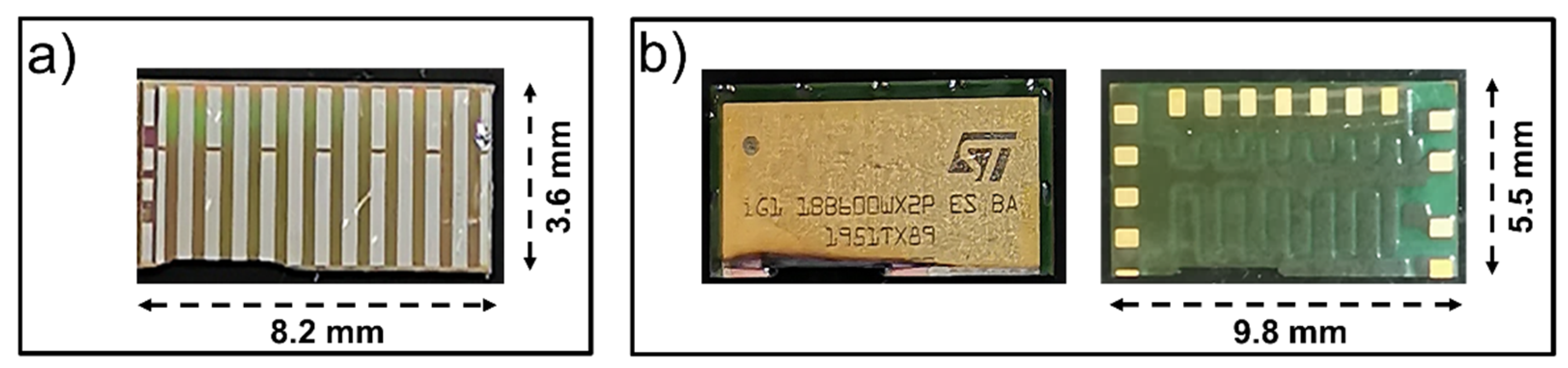
Figure 2.
Schematic representation of the internal structure of AlGaN/GaN HEMT-B (a) and AlGaN/GaN HEMT-PD (b) investigated in this study (not to scale). The vertical dashed line indicates the uniaxial direction along which micro-Raman measurements were performed.
Figure 2.
Schematic representation of the internal structure of AlGaN/GaN HEMT-B (a) and AlGaN/GaN HEMT-PD (b) investigated in this study (not to scale). The vertical dashed line indicates the uniaxial direction along which micro-Raman measurements were performed.
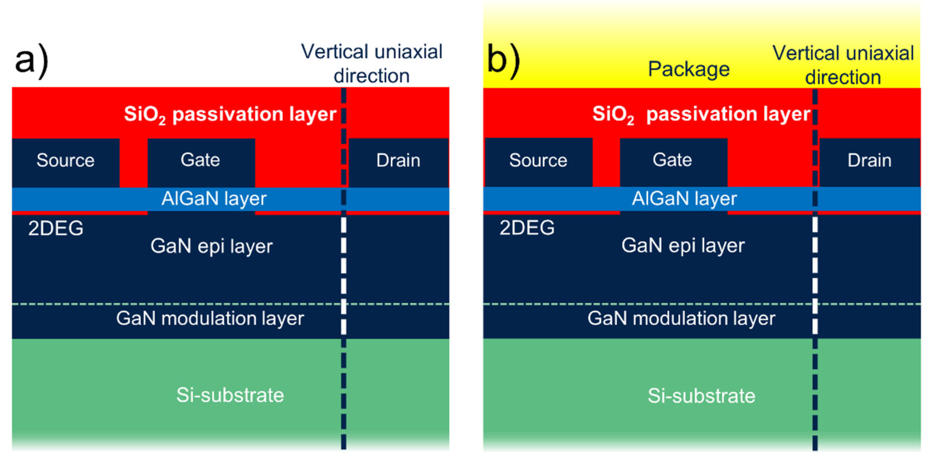
Figure 3.
Image of the sample holder (a) with details highlighting the sample position (b).
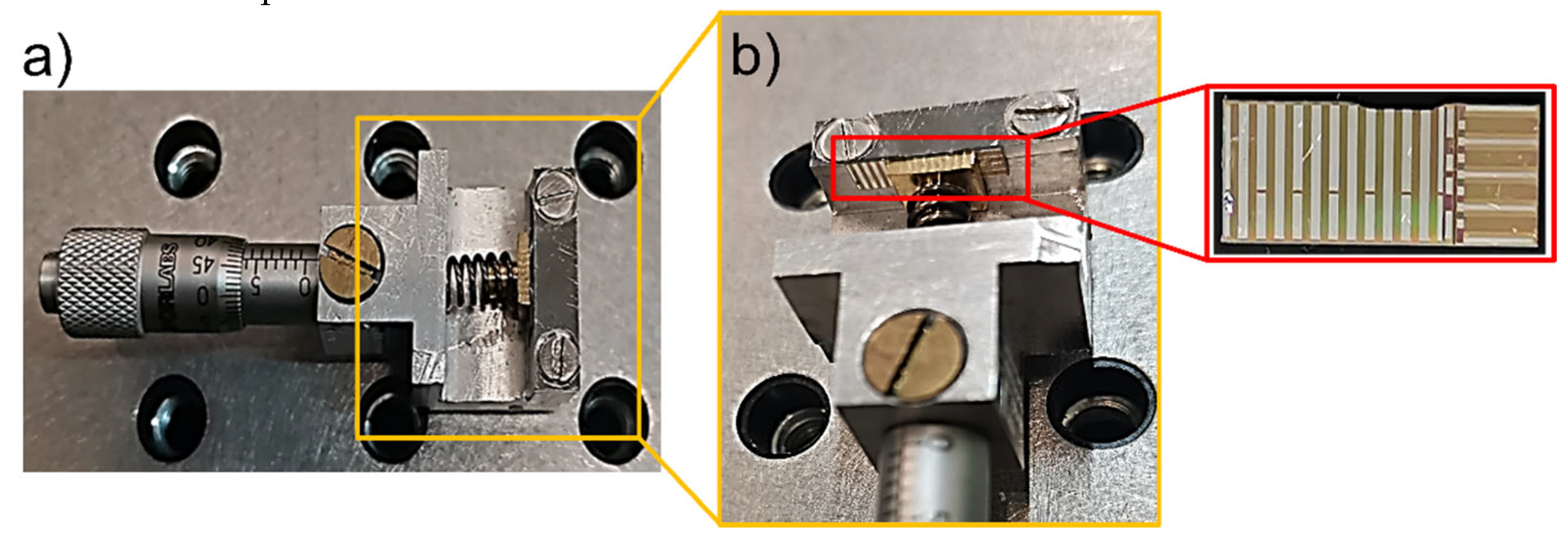
Figure 4.
Detailed view of the AlGaN/GaN HEMT-PD heterostructure (4a), and the resulting Raman map along the 10 µm scanned path (4b).
Figure 4.
Detailed view of the AlGaN/GaN HEMT-PD heterostructure (4a), and the resulting Raman map along the 10 µm scanned path (4b).
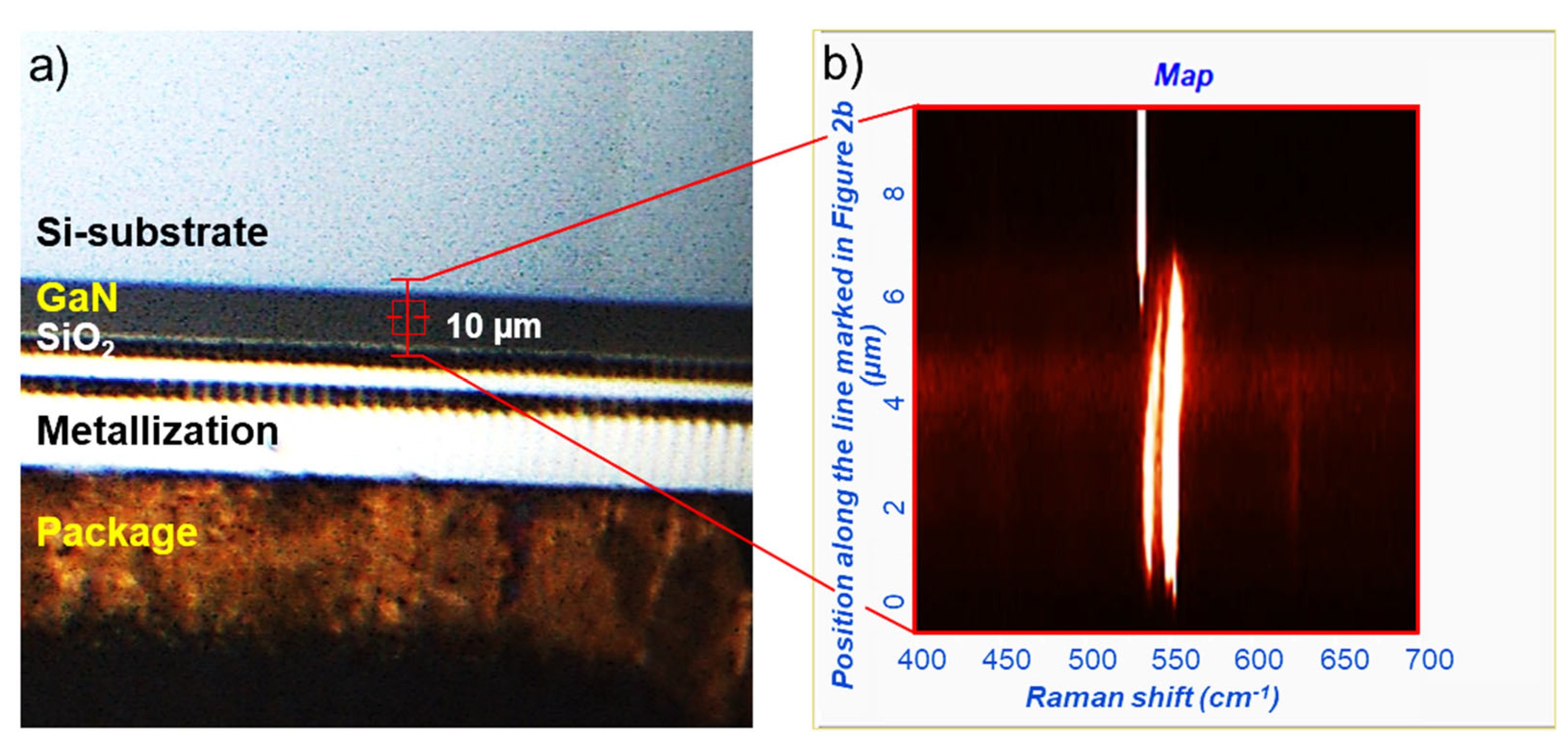
Figure 5.
Micro-Raman spectra collected at the GaN epitaxy layer (a) and at the GaN/Si interface (b) of HEMT-B.
Figure 5.
Micro-Raman spectra collected at the GaN epitaxy layer (a) and at the GaN/Si interface (b) of HEMT-B.
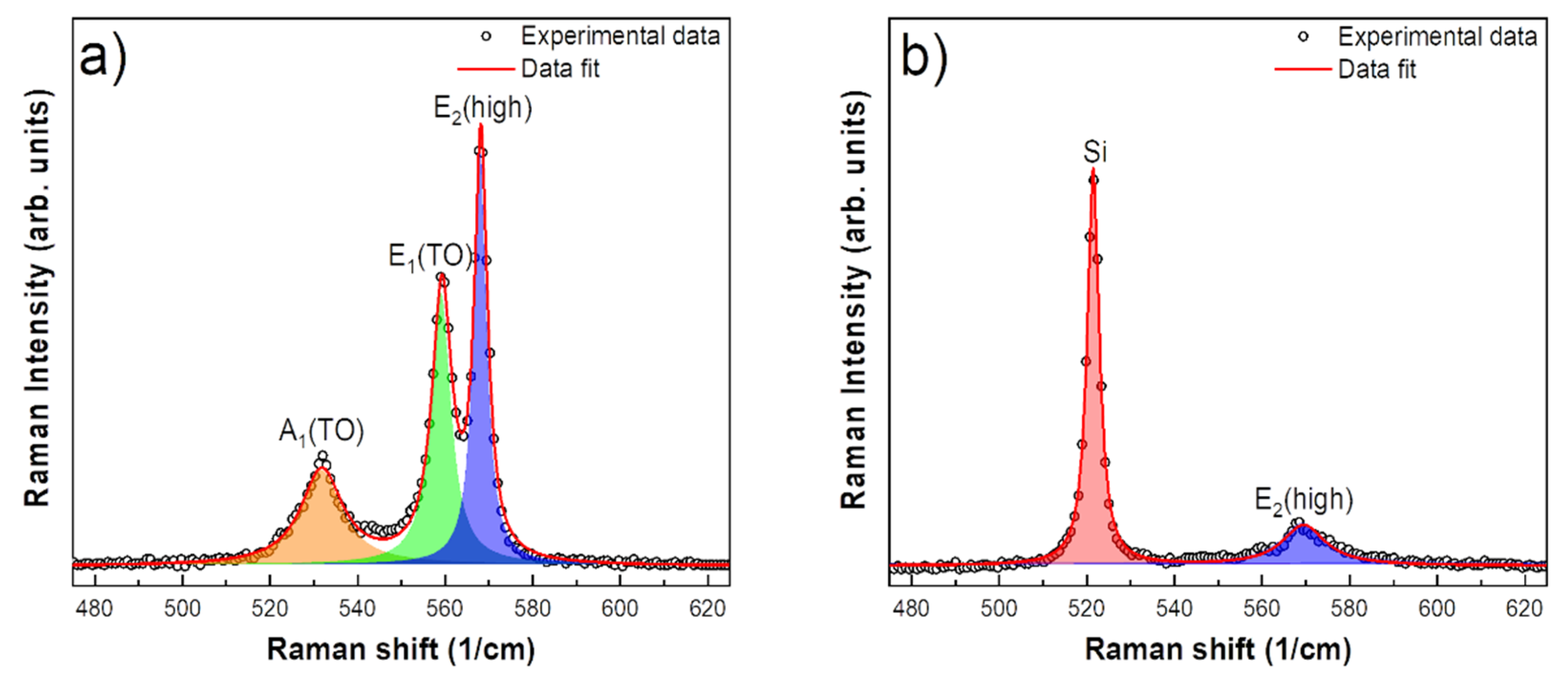
Figure 6.
Stress distribution along the uniaxial direction, covering a range from 5 µm to 7 µm within the GaN layer, for both AlGaN/GaN HEMT-B and AlGaN/GaN HEMT-PD devices. The inset graph represents the E2(high) peak frequency center plotted against the position along the uniaxial direction in µm.
Disclaimer/Publisher’s Note: The statements, opinions and data contained in all publications are solely those of the individual author(s) and contributor(s) and not of MDPI and/or the editor(s). MDPI and/or the editor(s) disclaim responsibility for any injury to people or property resulting from any ideas, methods, instructions or products referred to in the content. |
© 2024 by the authors. Licensee MDPI, Basel, Switzerland. This article is an open access article distributed under the terms and conditions of the Creative Commons Attribution (CC BY) license (http://creativecommons.org/licenses/by/4.0/).
Copyright: This open access article is published under a Creative Commons CC BY 4.0 license, which permit the free download, distribution, and reuse, provided that the author and preprint are cited in any reuse.


