Submitted:
09 February 2024
Posted:
13 February 2024
You are already at the latest version
Abstract
Keywords:
1. Introduction
- annealing temperature - the highest maintained temperature over a process
- pressure - uniaxial pressure applied to the sample during the sintering process
- time of highest temperature hold step.
2. Materials and Methods
2.1. Materials
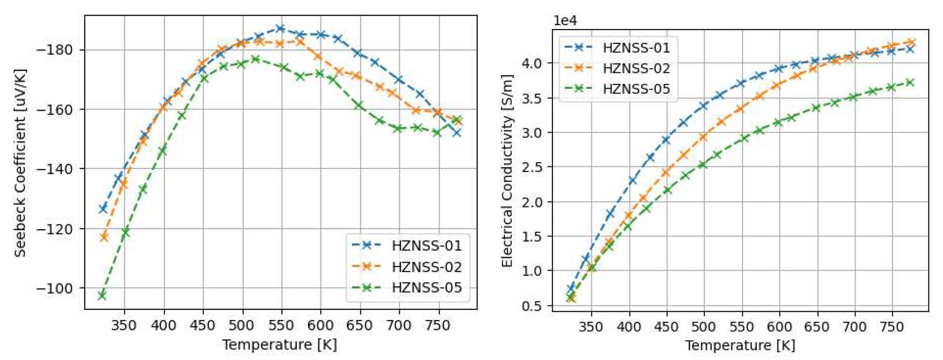
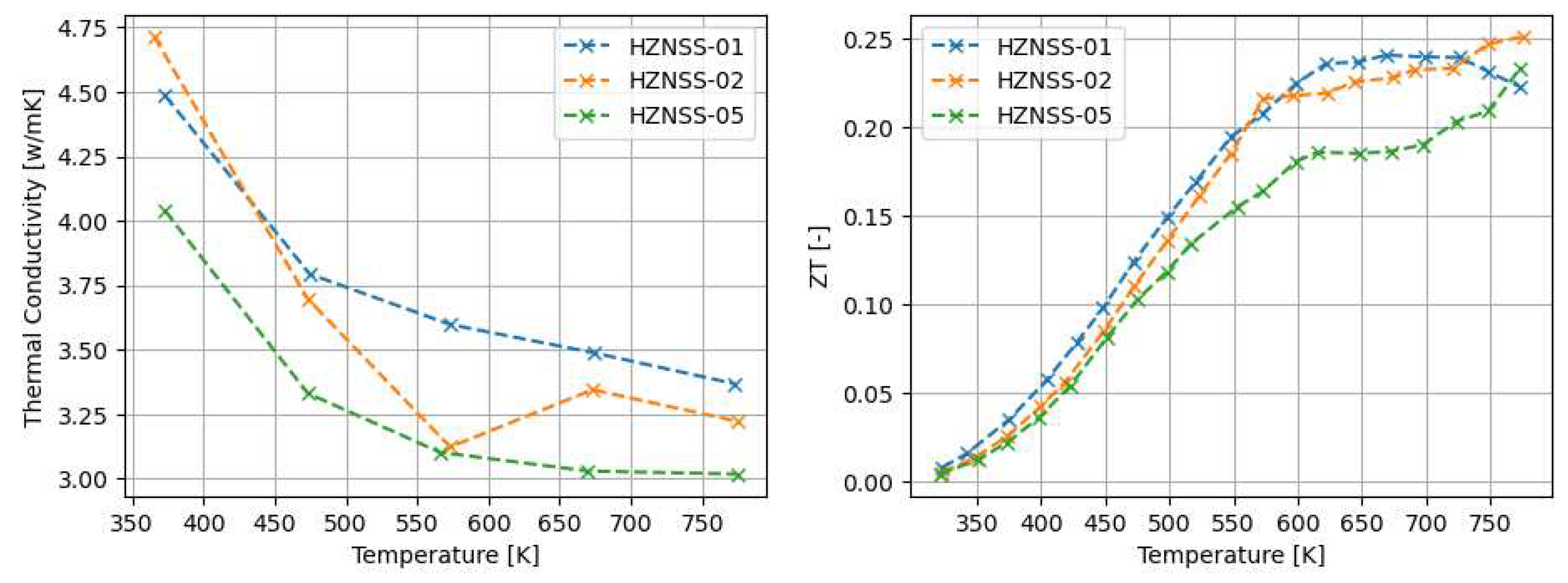
- Arc-Melted semiconductor materials, HCST-x () for x=[0, 0.01, 0.02, 0.05, 0.10] and HZNSS-x ( for x=[0.01, 0.02, 0.05])
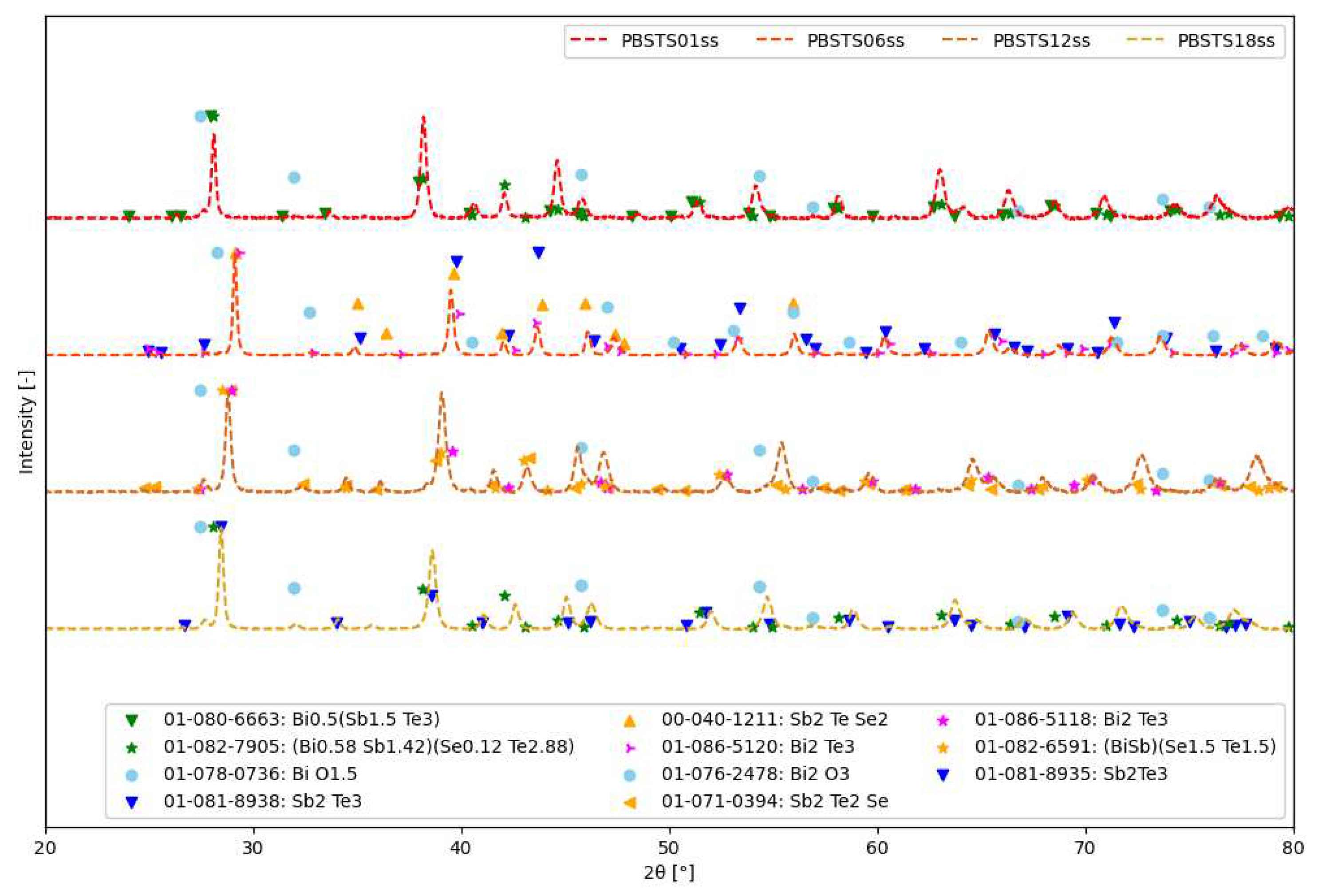
- Bismuth-telluride based materials synthesized by SHS technique mateirals (PBSTS-xxs). The reference material (PBSTq), fabricated inside quartz vacuum tube is also included for comparison of properties of SHS serie.
2.2. SPS system
2.3. Arc Melting of half-Heusler and cobalt triantimonide
- cobalt triantimonide: T=650°C, P=50MPa, time=15min
- half-Heusler: T=1000°C, P=50MPa, time=25min.
2.4. Thermal and electrical parameters characterization
2.5. XRD diffraction
2.6. SHS Synthesis
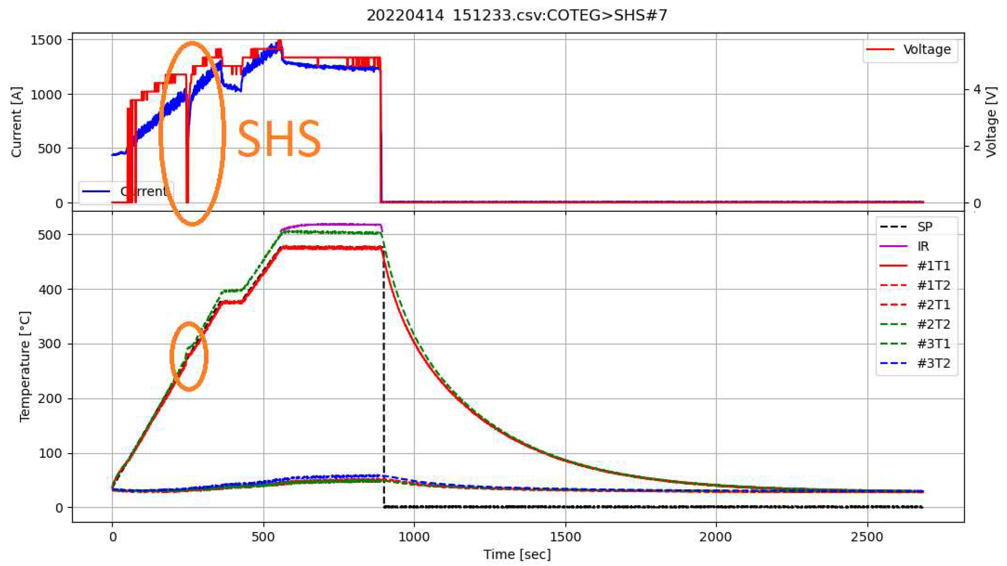
- Heating the reactor to 375°C and maintaining this temperature for 60 seconds. This step realizes the first, exothermic stage of materials synthesis (SHS occurs during the first initial heating)
- Heating material to 475°C and maintaining this temperature for 300 seconds. This step was applied to fully react reagents and homogenize material
2.7. Process data collection and device upgrade
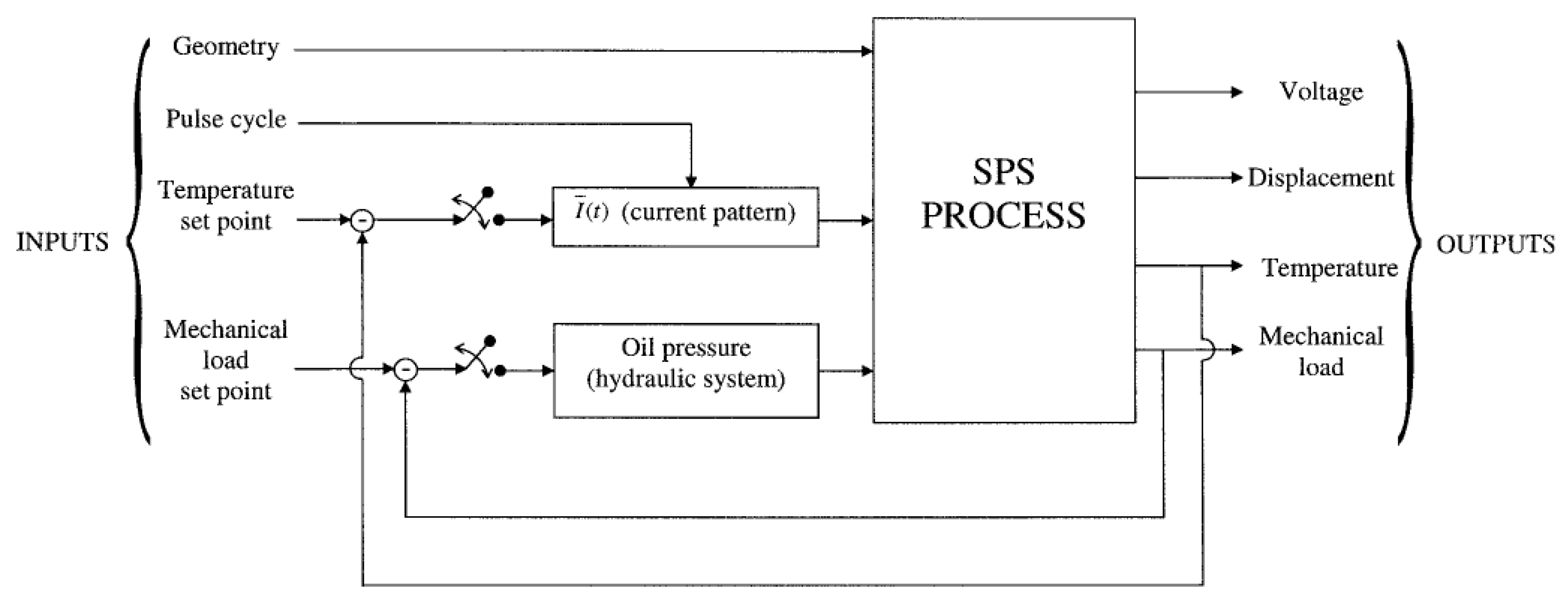
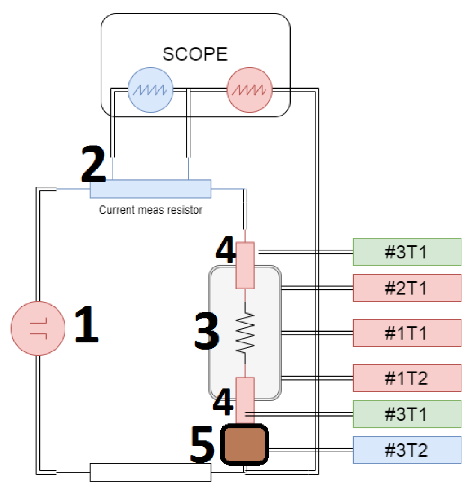
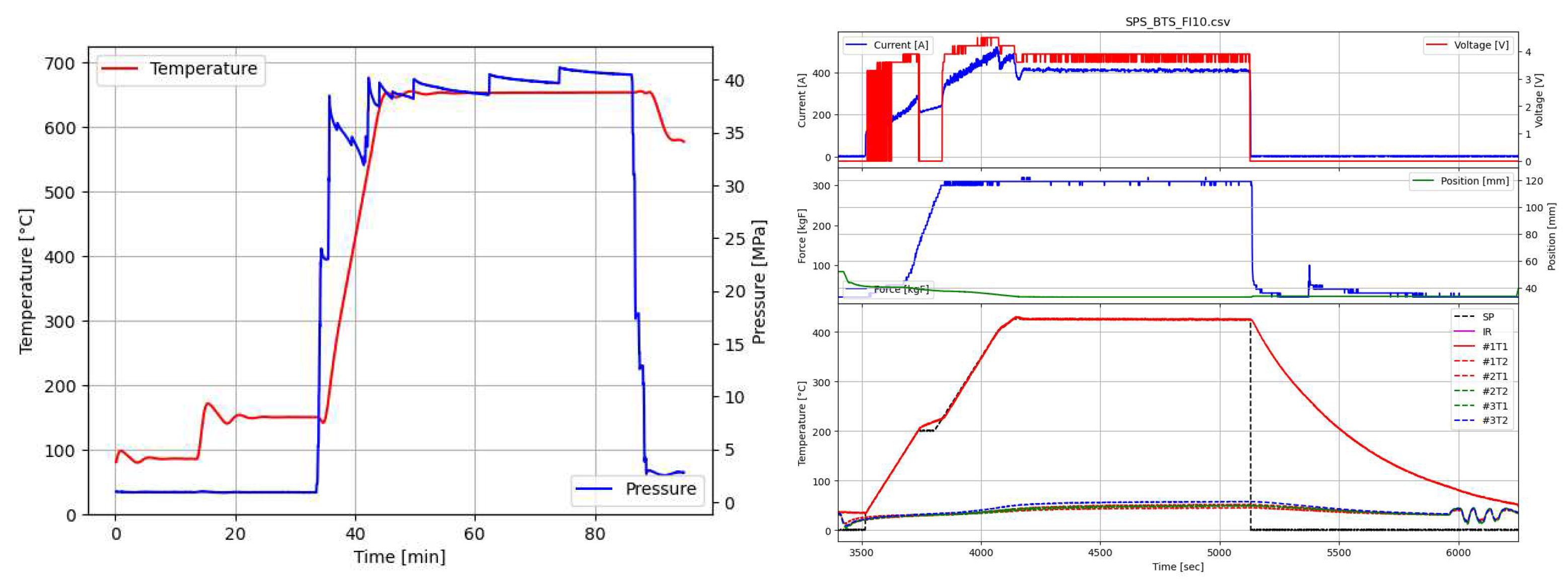
- Acquisition of power supply parameters (voltage and current), allowed to gain information about delivered power and, in some cases, the resistance of the sintering system.
- Constant stabilization of pressing force. A hysteresis regulator was used previously, causing lower reproducibility of pressure value over time. Now 5-way proportional valve driven by a quasi-logic controller is installed, allowing high stability and reproducibility of stabilized pressure.
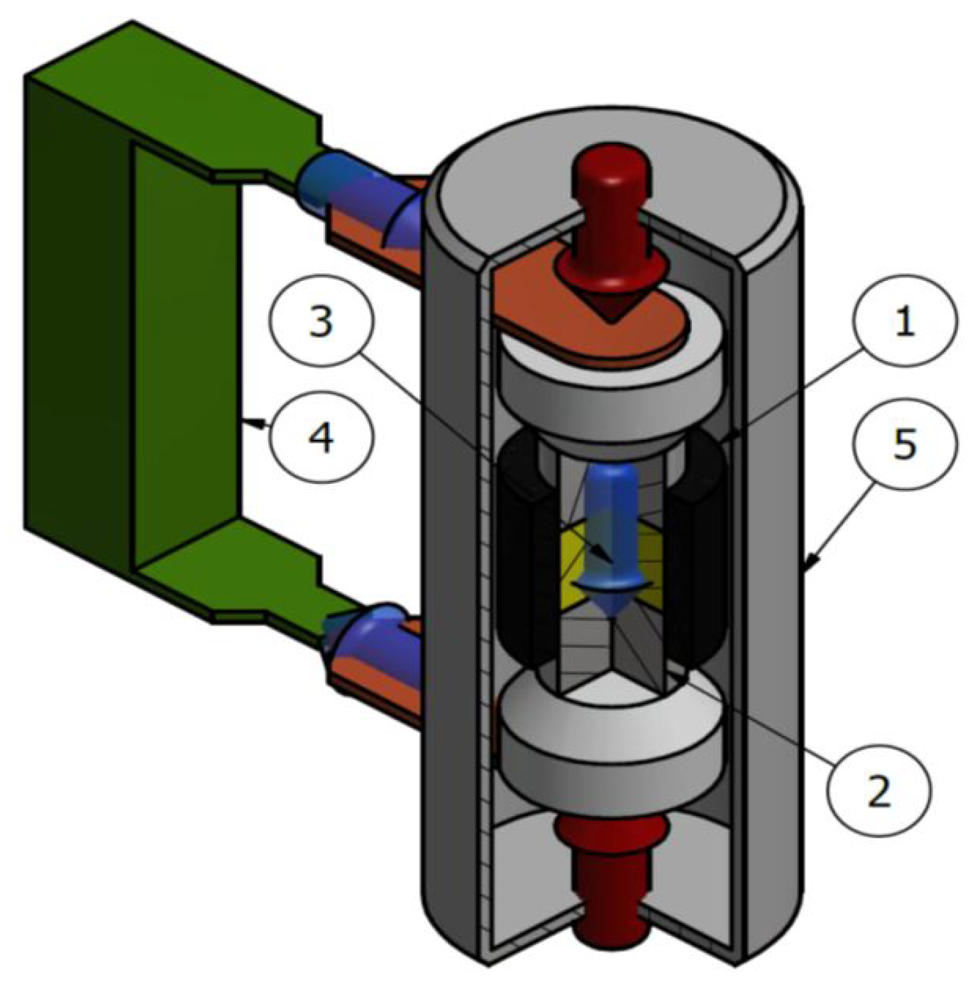
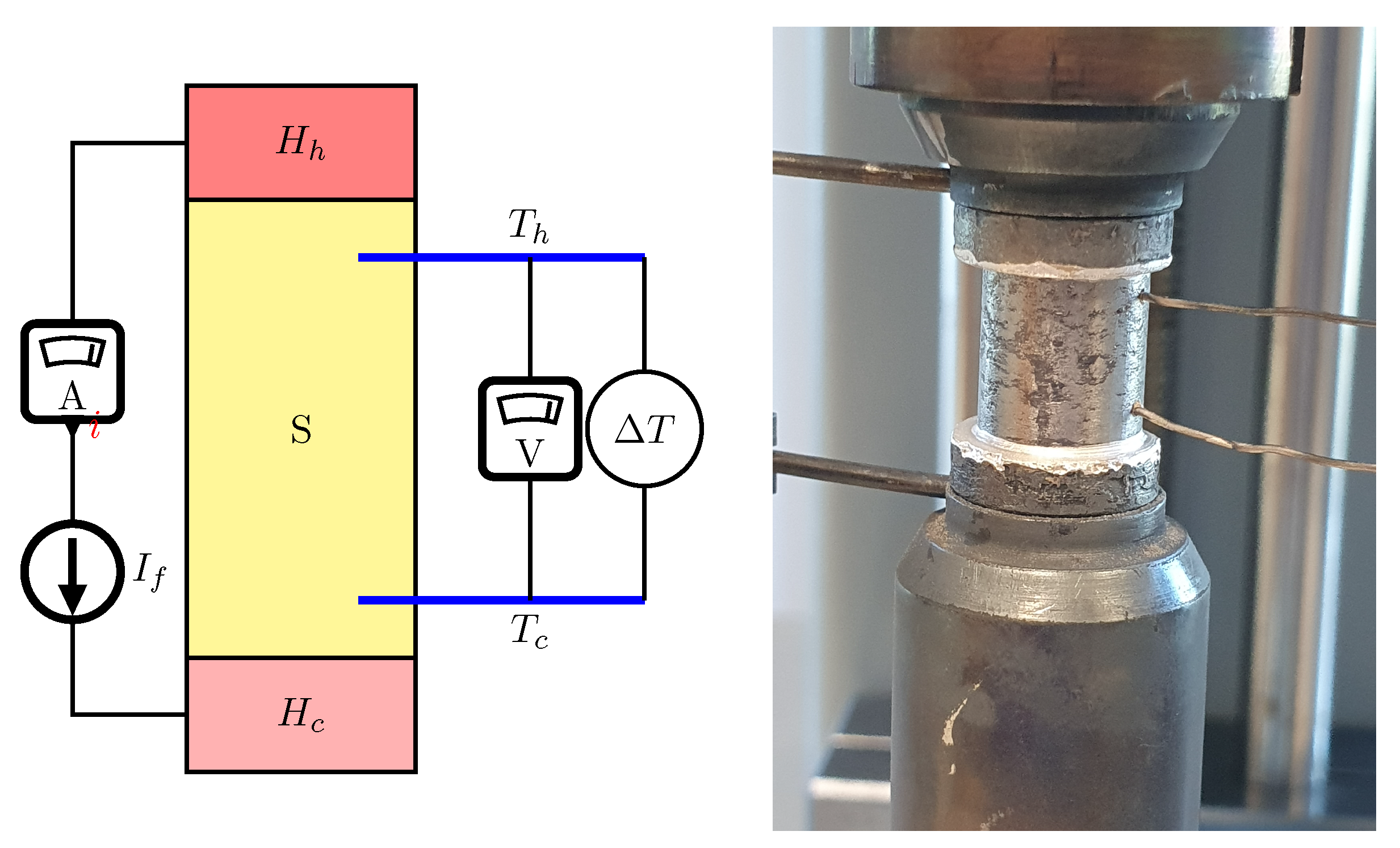
- Up to 6 thermocouples can be connected to determine the temperature gradient over the sample up to 950°C.
- Above 500°C, infrared temperature measurement can be used. The infrared curve shows when the temperature exceeds 500°C (Figure 4)
3. Results
3.1. Thermoelectric properties of arc-melted and sps-sintered materials
3.2. SHS synthesis results
3.2.1. Analysis of stages of SHS synthesis
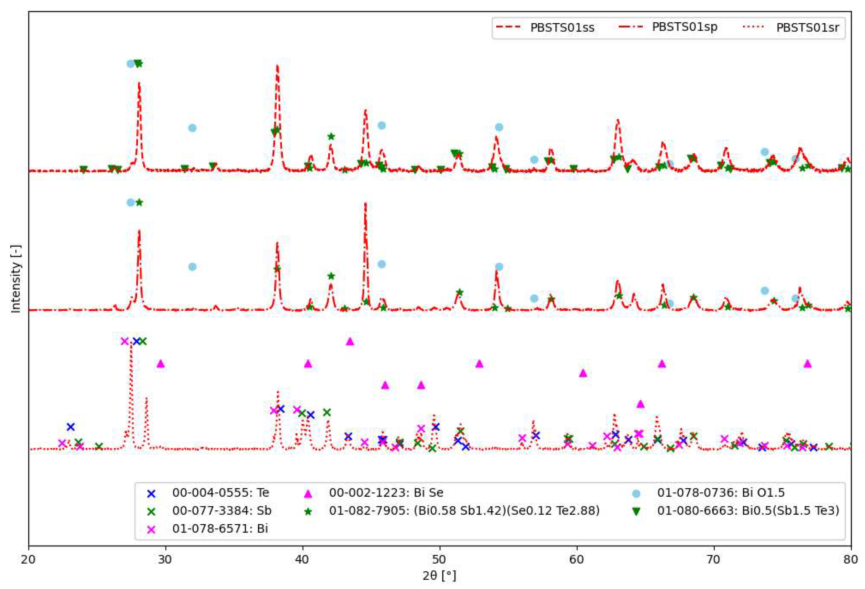
- PBSTS01sr - Material after the homogenization process in an automatic mortar. The analysis of the phase composition, in addition to confirming the presence of pure elements, i.e. tellurium (00-004-0555), antimony (00-077-3384) and bismuth (01-078-6571), also showed the presence of bismuth selenide (00-002-1223) in materials with higher selenium amount.
- PBSTS01sp - the fragmented material after synthesis SHS consisted mainly of the phase (01-082-7905 ) and bismuth oxide (01-078-0736). Some of the reflections are difficult to distinguish due to their overlap.
- PBSTS01ss - the material after sintering using the SPS technique contained the phase and, probably, bismuth oxide (01-078-0736)
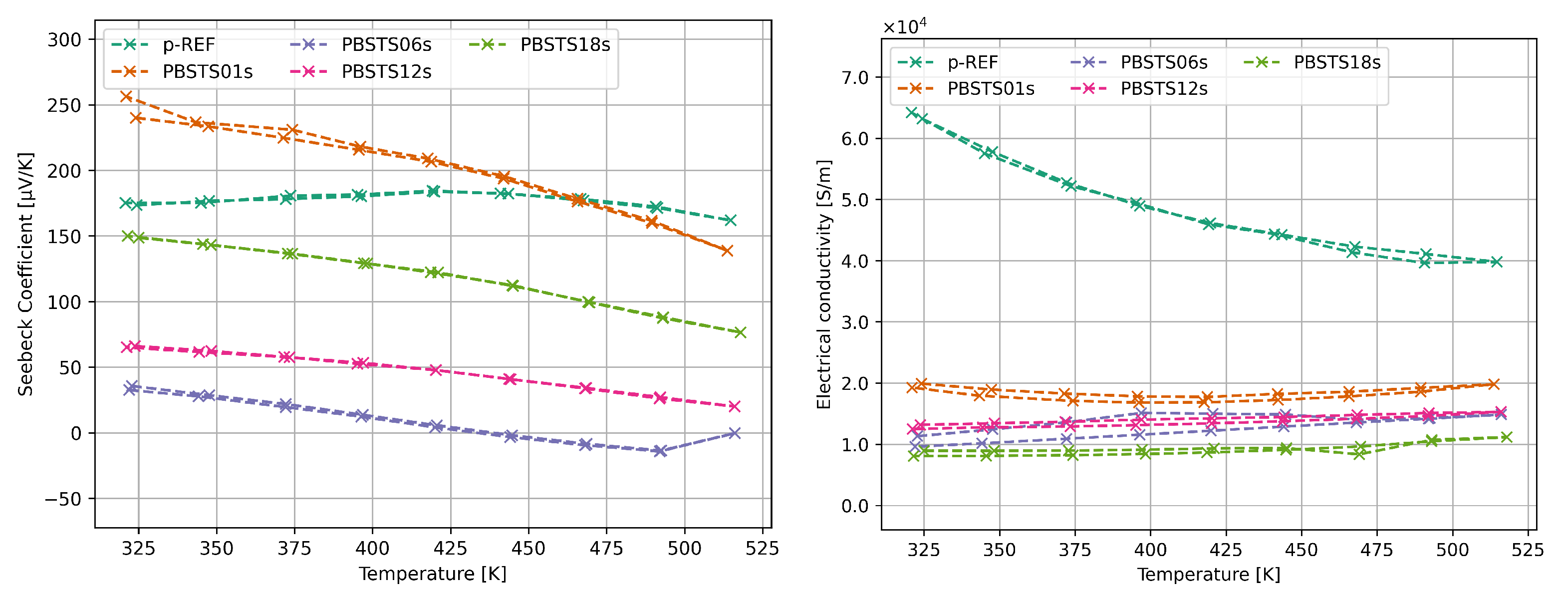
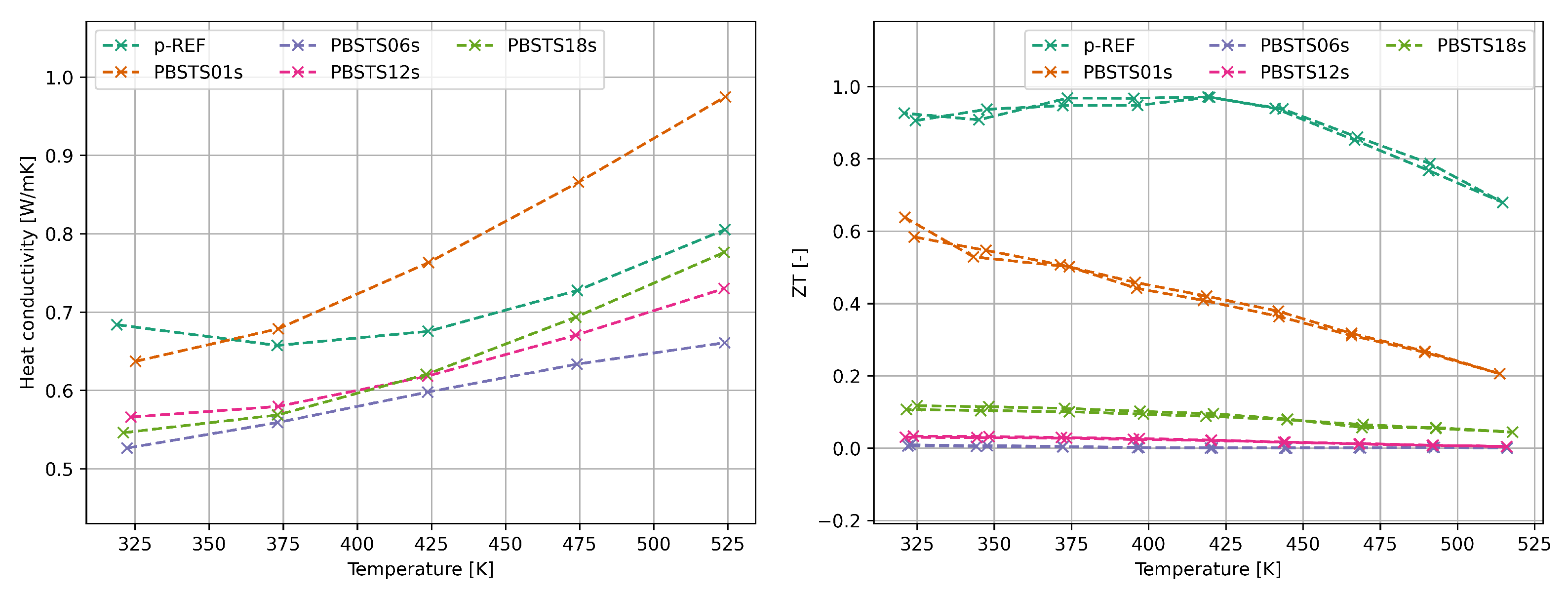
3.2.2. Thermoelectric properties of SHS synthesized bismuth telluride
4. Discussion
4.1. The properties of Arc-Melted materials
4.2. SHS synthesis
4.3. Thermoelectric properties of SHS materials
5. Conclusions
Author Contributions
Funding
Institutional Review Board Statement
Acknowledgments
Conflicts of Interest
Abbreviations
| SPS | Spark Plasma Sintering |
| SHS | Self-propagating high-temperature synthesis |
| AM | Arc-Melting |
| ZT | Thermoelectric Figure-of-merit |
References
- Ratzker, B.; Sokol, M. Exploring the capabilities of high-pressure spark plasma sintering (HPSPS): A review of materials processing and properties. Materials and Design 2023, 233, 112238. [Google Scholar] [CrossRef]
- Cincotti, A.; Locci, A.; Orrù, R.; Cao, G. Modeling of SPS apparatus: Temperature, current and strain distribution with no powders. AIChE journal 2007, 53, 703–719. [Google Scholar] [CrossRef]
- Stuer, M.; Bowen, P.; Zhao, Z. Spark Plasma Sintering of Ceramics: From Modeling to Practice. Ceramics 2020, 3, 476–493. [Google Scholar] [CrossRef]
- Nosewicz, S.; Jurczak, G.; Chrominski, W.; Rojek, J.; Kaszyca, K.; Chmielewski, M. Combined EBSD and Computer-Assisted Quantitative Analysis of the Impact of Spark Plasma Sintering Parameters on the Structure of Porous Materials. Metallurgical and Materials Transactions A 2022, 53, 4101–4125. [Google Scholar] [CrossRef]
- Saleemi, M.; Toprak, M.S.; Li, S.; Johnsson, M.; Muhammed, M. Synthesis, processing, and thermoelectric properties of bulk nanostructured bismuth telluride (Bi2Te3). J. Mater. Chem. 2012, 22, 725–730. [Google Scholar] [CrossRef]
- Lim, S.S.; Jung, S.J.; Kim, B.K.; Kim, D.I.; Lee, B.H.; Won, S.O.; Shin, J.; Park, H.H.; Kim, S.K.; Kim, J.S.; Baek, S.H. Combined hot extrusion and spark plasma sintering method for producing highly textured thermoelectric Bi2Te3 alloys. Journal of the European Ceramic Society 2020, 40, 3042–3048. [Google Scholar] [CrossRef]
- Kim, H.S.; Liu, W.; Chen, G.; Chu, C.W.; Ren, Z. Relationship between thermoelectric figure of merit and energy conversion efficiency. Proceedings of the National Academy of Sciences 2015, 112, 8205–8210. [Google Scholar] [CrossRef] [PubMed]
- Park, O.; Park, S.J.; Kim, H.S.; Lee, S.W.; Heo, M.; il Kim, S. Enhanced thermoelectric transport properties of Bi2Te3 polycrystalline alloys via carrier type change arising from slight Pb doping. Materials Science in Semiconductor Processing 2023, 166, 107723. [Google Scholar] [CrossRef]
- Hu, X.; Fan, X.; Feng, B.; Kong, D.; Liu, P.; Xu, C.; Kuang, Z.; Li, G.; Li, Y. Decoupling Seebeck coefficient and resistivity, and simultaneously optimizing thermoelectric and mechanical performances for n-type BiTeSe alloy by multi-pass equal channel angular extrusion. Materials Science and Engineering: B 2021, 263, 114846. [Google Scholar] [CrossRef]
- Dongre, B.; Carrete, J.; Wen, S.; Ma, J.; Li, W.; Mingo, N.; Madsen, G.K.H. Combined treatment of phonon scattering by electrons and point defects explains the thermal conductivity reduction in highly-doped Si. Journal of Materials Chemistry A 2020, 8, 1273–1278. [Google Scholar] [CrossRef]
- Mao, J.; Niedziela, J.L.; Wang, Y.; Xia, Y.; Ge, B.; Liu, Z.; Zhou, J.; Ren, Z.; Liu, W.; Chan, M.K.; Chen, G.; Delaire, O.; Zhang, Q.; Ren, Z. Self-compensation induced vacancies for significant phonon scattering in InSb. Nano Energy 2018, 48, 189–196. [Google Scholar] [CrossRef]
- d?Angelo, M.; Galassi, C.; Lecis, N. Thermoelectric Materials and Applications: A Review. Energies 2023, 16. [Google Scholar] [CrossRef]
- Marchenkov, V.V.; Lukoyanov, A.V.; Baidak, S.T.; Perevalova, A.N.; Fominykh, B.M.; Naumov, S.V.; Marchenkova, E.B. Electronic Structure and Transport Properties of Bi2Te3 and Bi2Se3 Single Crystals. Micromachines 2023, 14. [Google Scholar] [CrossRef] [PubMed]
- Yang, J.; Aizawa, T.; Yamamoto, A.; Ohta, T. Thermoelectric properties of n-type (Bi2Se3)x(Bi2Te3)1?x prepared by bulk mechanical alloying and hot pressing. Journal of Alloys and Compounds 2000, 312, 326–330. [Google Scholar] [CrossRef]
- Bucholc, B.; Kaszyca, K.; ?piewak, P.; Mars, K.; Kruszewski, M.J.; Ciupi?ski, u.; Kowiorski, K.; Zyba?a, R. Thermoelectric properties of bismuth-doped magnesium silicide obtained by the self-propagating high-temperature synthesis. Bulletin of the Polish Academy of Sciences Technical Sciences 2022, 70, e141007. [Google Scholar] [CrossRef]
- Liu, R.; Tan, X.; Ren, G.; Liu, Y.; Zhou, Z.; Liu, C.; Lin, Y.; Nan, C. Enhanced Thermoelectric Performance of Te-Doped Bi2Se3?xTex Bulks by Self-Propagating High-Temperature Synthesis. Crystals 2017, 7. [Google Scholar] [CrossRef]
- Zheng, G.; Su, X.; Liang, T.; Lu, Q.; Yan, Y.; Uher, C.; Tang, X. High thermoelectric performance of mechanically robust n-type Bi2Te3?xSex prepared by combustion synthesis. Journal of Materials Chemistry A 2015, 3, 6603–6613. [Google Scholar] [CrossRef]
- R. Knight, R.W.S.; Apelian, D. Application of plasma arc melting technology to processing of reactive metals. International Materials Reviews 1991, 36, 221–252. [Google Scholar] [CrossRef]
- Aversano, F.; Palumbo, M.; Ferrario, A.; Boldrini, S.; Fanciulli, C.; Baricco, M.; Castellero, A. Role of secondary phases and thermal cycling on thermoelectric properties of TiNiSn half-Heusler alloy prepared by different processing routes. Intermetallics 2020, 127, 106988. [Google Scholar] [CrossRef]
- Zhang, J.; Hu, Y.; Wei, Q.; Xiao, Y.; Chen, P.; Luo, G.; Shen, Q. Microstructure and mechanical properties of RexNbMoTaW high-entropy alloys prepared by arc melting using metal powders. Journal of Alloys and Compounds 2020, 827, 154301. [Google Scholar] [CrossRef]
- Cieslak, J.; Tobola, J.; Berent, K.; Marciszko, M. Phase composition of AlxFeNiCrCo high entropy alloys prepared by sintering and arc-melting methods. Journal of Alloys and Compounds 2018, 740, 264–272. [Google Scholar] [CrossRef]
- Zhang, J.; Xiong, K.; Huang, L.; Xie, B.; Ren, D.; Tang, C.; Feng, W. Effect of Doping with Different Nb Contents on the Properties of CoCrFeNi High-Entropy Alloys. Materials 2023, 16. [Google Scholar] [CrossRef]
- Yamada, O.; Miyamoto, Y.; Koizumi, M. Self-Propagating High-Temperature Synthesis (SHS) of SiC Powders and the Properties of the Sintered Compact. Journal of the Japan Society of Powder and Powder Metallurgy 1986, 33, 286–290. [Google Scholar] [CrossRef]
- Moskovskikh, D.O.; Mukasyan, A.S.; Rogachev, A.S. Self-propagating high-temperature synthesis of silicon carbide nanopowders. Doklady Physical Chemistry 2013, 449, 41–43. [Google Scholar] [CrossRef]
- Yasenchuk, Y.; Marchenko, E.; Gunther, V.; Radkevich, A.; Kokorev, O.; Gunther, S.; Baigonakova, G.; Hodorenko, V.; Chekalkin, T.; Kang, J.h.; Weiss, S.; Obrosov, A. Biocompatibility and Clinical Application of Porous TiNi Alloys Made by Self-Propagating High-Temperature Synthesis (SHS). Materials 2019, 12. [Google Scholar] [CrossRef] [PubMed]
- Kruszewski, M.; Kot, M.; Cymerman, K.; Chmielewski, M.; Moszczy?ska, D.; Ma?ek, M.; Ciupi?ski. Rapid fabrication of Se-modified skutterudites obtained via self-propagating high-temperature synthesis and pulse plasma sintering route. Ceramics International 2023, 49, 9560–9565. [Google Scholar] [CrossRef]
- Min, S.; Blumm, J.; Lindemann, A. A new laser flash system for measurement of the thermophysical properties. Thermochimica Acta 2007, 455, 46–49. [Google Scholar] [CrossRef]
- Ratzker, B.; Sokol, M.; Kalabukhov, S.; Frage, N. Creep of Polycrystalline Magnesium Aluminate Spinel Studied by an SPS Apparatus. Materials 2016, 9. [Google Scholar] [CrossRef] [PubMed]
- Qiu, J.; Yan, Y.; Xie, H.; Luo, T.; Xia, F.; Yao, L.; Zhang, M.; Zhu, T.; Tan, G.; Su, X.; Wu, J.; Uher, C.; Jiang, H.; Tang, X. Achieving superior performance in thermoelectric Bi0.4Sb1.6Te3.72 by enhancing texture and inducing high-density line defects. Science China Materials 2021, 64, 1507–1520. [Google Scholar] [CrossRef]
- Guo, X.; Jia, X.; Jie, K.; Sun, H.; Zhang, Y.; Sun, B.; Ma, H. Thermoelectric transport properties and crystal growth of BiSbTe3 bulk materials produced by a unique high-pressure synthesis. CrystEngComm 2013, 15, 7236–7242. [Google Scholar] [CrossRef]
- Zhai, R.S.; Wu, Y.H.; Zhu, T.J.; Zhao, X.B. Thermoelectric performance of p-type zone-melted Se-doped Bi0.5Sb1.5Te3 alloys. Rare Metals 2018, 37, 308–315. [Google Scholar] [CrossRef]
| Identification | Chemical formula | Processing method |
|---|---|---|
| HCST-01 | AM, SPS | |
| HCST-02 | AM, SPS | |
| HCST-05 | AM, SPS | |
| HCST-10 | AM, SPS | |
| HZNZZ-01 | AM, SPS | |
| HZNZZ-02 | AM, SPS | |
| HZNZZ-05 | AM, SPS | |
| PBSTq (pREF) | Melting, SPS | |
| PBSTS-01s | SHS, SPS | |
| PBSTS-06s | SHS, SPS | |
| PBSTS-12s | SHS, SPS | |
| PBSTS-18s | SHS, SPS |
| Parameter | Value/Range | unit |
|---|---|---|
| Operating temperature | RT-2000 | °C |
| Sample diameter | 10-501 | mm |
| Power supply max. current | 5000 | A |
| Power supply max. voltage | 10 | V |
| Ultimate vacuum | mBar | |
| Pressing force (max) | 10 | Tons |
Disclaimer/Publisher’s Note: The statements, opinions and data contained in all publications are solely those of the individual author(s) and contributor(s) and not of MDPI and/or the editor(s). MDPI and/or the editor(s) disclaim responsibility for any injury to people or property resulting from any ideas, methods, instructions or products referred to in the content. |
© 2024 by the authors. Licensee MDPI, Basel, Switzerland. This article is an open access article distributed under the terms and conditions of the Creative Commons Attribution (CC BY) license (http://creativecommons.org/licenses/by/4.0/).


