Submitted:
23 January 2024
Posted:
25 January 2024
You are already at the latest version
Abstract
With continued scaling of semiconductor devices , the value of predictive analysis through 1 accurate quantum transport modeling is exponentially increasing. Quantum transmitting Boundary 2 method (QTBM) has been a well-known method of choice to model quantum transport in simple 1-D 3 devices. Here, we present an extension of the QTBM to the 2-D domain and apply it for more realistic 4 devices for accurate performance analysis.
Keywords:
quantum transport
; QTBM
; Schrodinger equation
; Poisson equation
; Device Physics
; 6 Solid State Physics
1. Introduction
With continued scaling of semiconductor devices to meet the aggressive goals set forth by the International Technology Roadmap for Semiconductors (ITRS) [1], cost of fabrication are exponentially increasing, adding equivalent value to the power of predictive analysis through accurate modeling. Moreover, due to aggressive scaling of device dimensions, quantum transport is gradually becoming the dominant transport mechanism for carriers. The current generation of transistors [2,3,4,5,6,7,8,9] have active regions of length comparable to the wavelength of an electron. At such small dimensions, the basic assumption of the semi-classical transport physics [10,11], that electrons are point-like objects with defined position and momentum, falls short. A full quantum study of electron transport is needed to simulate and understand the behavior of these devices, including explicit quantum mechanical effects like tunneling, quantization and resonance [12,13,14,15].
The three well-known methods to study quantum transport are the Wigner function method [16,17,18], the Non-equilibrium Green’s function method [19,20,21,22,23] and the self-consistent solution of the Schrödinger, Pauli master [24,25,26] and Poisson equations. In our research we will be using the latter to model ballistic and dissipative electron transport. The model we employ uses the single-electron envelope approximation and the conduction bands are approximated with parabolic ellipsoidal or spherical valleys (six ellipsoidal valleys in the case of silicon). In particular, we are extending the popular Quantum Transmitting Boundary method (QTBM) for solving the two-dimensional Schrödinger equation and therefore validate its application towards behavior analysis of more realistic devices.
2. Simulation Methodology
Our main objective is to solve a system that can communicate with its environment through its contacts, namely an open system [27]. This requires discretizing the continuum of energies in the contacts. The optimal discretization is obtained by sampling the density-of-states using the solution of the system in equilibrium, namely a closed system [28,29]. Section 2.1 details our theoretical scheme of obtaining these solutions of the closed system. We solve the Schrödinger equation with closed boundary conditions self-consistently [30,31] with the Poisson equation in the two-dimensional (2-D) plane of the device to achieve this. The device is assumed wide enough so that a 3-D simulation is not required. In Section 2.3, our simulation methodology is extended to model an open system driven far from equilibrium under the influence of a drain-to-source bias. The Quantum Transmitting Boundary method (QTBM) [32,33] is used to enforce open boundary conditions to model particle exchange, through current-carrying leads, between the device and environment. Furthermore, ways to derive various device characteristics of practical importance are highlighted here. Finally we provide an application for our ballistic simulation tool.
We start with the equilibrium condition of the system. This is obtained by solving the two-dimensional (2-D) Schrödinger and Poisson equations self consistently [30] for different gate biases and at different temperatures, with no drain-to-source voltage applied. For very wide devices, we can assume translational invariance of the device profile along the out-of-plane y direction and therefore our 2-D approach is a good approximation. We define this closed state of the system as one in which the system does not exchange particles (and energy, thermodynamically) with the rest of the `universe’ through its contacts. Therefore, in its quantum description, either the wavefunctions must vanish outside the system or there should be zero net probability current entering or exiting the system. In order to obtain the correct closed system solution, it is better to solve the Schrödinger equation with both Dirichlet and Neumann boundary conditions, so that one gets the right density near the contacts and, so, the correct potential. The Dirichlet and Neumann solutions behave `sine-like’ and `cosine-like’ at the device-contact interface, respectively, as Figure 1 shows.
Thereby, a combined set of these two forms a complete set of physical solutions and any other solution to the closed system can be represented as a linear combination of the two. In all the cases, zero-value Dirichlet boundary conditions will be applied at the oxide-semiconductor interface as well as at the substrate of the device to account for the idealized yet physically consistent situation of having zero charges beyond the said interfaces.
Next, we describe how to obtain a self-consistent 2-D solution of the Schrödinger equation, considering both Dirichlet (Sec. 2.1) and QTBM boundary conditions (Sec. 2.3), and Poisson equations. When solving the Poisson equation, in order to account for electrostatic control through gates using externally applied bias, Dirichlet boundary conditions are applied at the gate-dielectric interfaces, while Neumann conditions are imposed elsewhere to ensure confinement of the electric field to the simulation domain.
2.1. Two-Dimensional Schrödinger Equation Solution for Quasi-static Charge Distribution
The time-independent single electron `effective mass’ Luttinger-Kohn (Schrödinger) equation [34] is solved using the parabolic-band approximation to account for the Silicon band structure. The numerical method of choice is the finite differences method. The Luttinger-Kohn equation can be written as:
where, using the effective mass approximation, and is the effective mass of band m. For Silicon channels oriented along the direction, the two-dimensional Schrödinger equation can be written as [30,35]:
where the envelope wavefunction is and , and are the transport mass (along transport x direction), the out-of-plane mass (along the y-direction into the plane of the device), and the quantization mass (along z, perpendicular to the carrier transport). V is the potential energy on the plane, is the energy of the two-dimensional wavefunction and represents the wavevector in the y direction. The superscript v is used to represent the different values taken by the annonated quantities for the six ellipsoidal valleys of the Si Brillouin zone All computations are repeated once for each pair of inequivalent valley-orientations.
The expression denotes the total energy of an electron state described by the wavefunction . Numerically, Eq. (2) can be recast as:
where , and, i is the index for the N discretized mesh points. We deploy a 2-D mesh obtained by the tensor product of two 1-D meshes consisting of and points, so that . The Hamiltonian matrix () is created using the terms on the left-hand-side of Eq. 3. Since we are modeling a closed system, the wavefunctions should vanish outside the device and therefore Dirichlet boundary conditions are assumed at the simulation boundaries. With these assumptions, Eq. (3) takes the form of an eigenvalue problem of rank N:
where and are the eigenfunction and eigenvalue, respectively, and, ranges from 1 to N. Incorporating non uniformity of the mesh, the Hamiltonian matrix () is given by:
where
and,
and are the matrix elements in row k and column l. actually gives wavefunctions that vanish just outside the device domain. All elements, except those on the diagonal, of the rows representing the left and right edges of the device, i.e., rows having indexes or (j being an integer within range ), are set to zero. This ensures application of zero-value Dirichlet boundary condition exactly at the left and right edge of the device. is a diagonal matrix containing the potential distribution, as shown below,
where the index i represents each mesh point.
Typically the <110> channel orientation is preferred for current-generation MOSFET devices due to added advantage/favorability towards hole mobility, while having relatively small negative impact on electron mobility [36]. In this case, the effective mass tensor becomes a matrix, instead of a relatively simpler diagonal matrix, resulting in the presence of mixed second-order derivatives in the Schrödinger equation.
Let and be the co-ordinate systems based on the and orientations, respectively. Based on simple geometry, we can write
Rotating the co-ordinate system from to by incorporating the above relations in Eq. (1) we obtain
We can express the solution as to remove the mixed 2nd order derivatives. Note here that we take into account the translational invariance of the potential in the direction by assuming a free electron solution in that direction. Substituting the guess solution in Eq. (9) we obtain,
Equating the coefficients of the first order derivatives w.r.t. x to 0,
giving , with and . Removing the `prime’ from the co-ordinate axes for convenience, the updated Schrödinger equation for representing transport in the direction then takes the form
where the full (envelope) wavefunction is given as
The electron wavefunctions (labeled by the index ) and the corresponding eigenvalues are determined by solving this eigenvalue problem.
The Schrödinger equation for <110> direction, Eq. (12), must be utilized to treat only four of the six conduction band Si valleys, since the in-plane rotation from the to the direction does not affect the other two valleys with . Here is the longitudinal effective mass and (used later) represents the transverse effective mass ( is the electron mass). These valleys can be treated using the relatively simpler expression given by Eq. (3). Note that the calculations, shown here for Si, can be extended for any other material with similar orientations of their conduction band minima (provided their band structure can considerably approximated by effective masses).
2.2. Determination of Carrier Concentration And Use in Poisson Equation
The electron wavefunctions obtained as eigen-solutions to the closed-system Hamiltonian are used to compute the electron charge distribution in the device. The information regarding the DoS along the x and z directions is already contained in these quantized 2-D wavefunctions. We have only to use the 1-D DoS representing the continuous energy spectrum along the ’homogenous’ out-of-plane y direction given by the expression
The expression for the electron charge distribution is
where and represent the wavefunction and energy of the electronic state , respectively. Using Eq. (14), the above expression becomes
Here is the Fermi-Dirac integral of order -1/2, computed numerically using the Gauss-Legendre quadrature method [37].
The hole charge distribution, , is calculated semiclassically using the following expression based on 3-D density-of-states,
where is the hole effective mass, the is the band gap energy of silicon, and, is the Fermi-Dirac integral of order 1/2 [37].
Note that the inclusion of temperature as an input parameter in the device simulation is achieved through the temperature dependence of Eqs. (16) and (17).
Here we briefly describe the numerical solution of Poisson equation which constitutes an important part of most transport simulations. We solve the Poisson equation in the 2-D plane of the device. To incorporate correctly the electrostatic effects caused by transitions in the electric permittivity along the semiconductor-dielectric interface, we solve the generalized Poisson equation:
where e is the electron charge and is the permittivity of the material present at . The centered finite-differences method is used to solve this linear system problem :
where is an matrix representing the differential operators on the left hand side of Eq. (19), and are matrices expressing the potential energy distribution and the charge terms on the right hand side of Eq. (18), respectively, for each of the N mesh points. Neumann boundary conditions are employed along all the domain boundaries. Here, the gate potential is applied by setting Dirichlet boundary conditions. Mathematically this is done by assigning zeros to all the elements of the rows representing the said portion of the oxide-metal interface, except for the diagonal elements where unity is assigned. The gate potential in electron volts is added to the corresponding rows of the charge matrix . This assignment might lead to singularity issues while solving the linear system Eq. (19) computationally. The solution consists in multiplying the unity diagonal terms on and the corresponding gate potential terms on by a factor that has the same order of magnitude as the other non-zero terms on . The Schrodinger and Poisson equations are solved selfconsistently following the flow highlighted in Figure 2.
2.3. 2-D Schrödinger Equation with Quantum Transmitting Boundary Method: Device Under Bias
Our main scenario of interest is the `open’ system in which electrons can flow into and out of the active region of the semiconductor device. This essentially describes the behavior of a device in the presence of an applied drain-to-source bias . The method we follow is the QTBM. [32]. The source and drain contacts are hypothesized as infinitely long leads culminating into the device, as shown schematically in Figure 3.
A distinct coordinate system is defined for each lead s, as shown in the figure. This is just a matter of convenience as the same derivations/expressions become applicable for all the leads. The potential is assumed to be constant along the direction while the potential profile along , is set equal to that along the lead-device interface. The wavefunction outside the system of leads and device is considered zero. Keeping these assumptions in mind, the wavefunctions within the leads can be broken into two independent components - traveling waves along and wavefunctions with a discretized energy spectrum along due to the quantum confinement in that direction. The latter part is computed by solving the 1-D Schrödinger equation along ,
where is the electron potential energy along in lead s and is the quantization mass. Eq. (20) becomes an eigenvalue problem as a consequence of the zero-value Dirichlet boundary conditions imposed by the lead edges. and represent the eigenstate and eigen-energy, respectively, in lead s of the one-dimensional (1-D) eigenvalue problem which can be written as,
where the 1-D Hamiltonian matrix is a tridiagonal matrix, built as follows:
The computed eigenstates are normalized along the direction and the total wavefunction inside lead s is then given by:
Here, the expression inside the first summation represent traveling waves with energy (along the x and z directions) , going into and reflecting out of the device, respectively, through the lead s. The index denotes the wavefunctions and the corresponding energies in the conduction band valley v. The expression within the second summation represents the gradually decaying modes with energy . The coefficients ’s are chosen as inputs for the different waves traveling into the device, while the coefficients need to be determined. For all other leads , the injection amplitudes . The wavevectors for the traveling modes are given by: and, for the evanescent modes, by: . The energy will be referred to as the `injection energy’. Note that depending on the left or right contact, respectively.
The boundary conditions at the interface between the device and lead s dictate the continuity of both the wavefunction at the interface, , and, the normal derivative, for all . Here denotes the wavefunction inside the device. Using Eq. (23) and combining the aforementioned boundary conditions together, we obtain:
Using finite-differences to discretize the right hand side of the above equation, we obtain
Now, multiplying both sides of Eq. (23) by and integrating over in the range , where is the vertical height of lead s, we obtain for ,
The wavefunctions are eigenstates of a Hermitian operator () and so are mutually orthogonal, . Using this relation and replacing with , observing continuity of the wavefunction at the interface, Eq. (26) gives us
Note that since evanescent waves are not injected, the above relation will not contain the term for . Eq. (25) can be re-written as:
In practice the wavefunctions are calculated separately for each injected traveling wave and thus they depend on m as well (a superscript m will be used to denote this dependence henceforth). In our problem it has been seen that the extent of numerical errors is reduced with the introduction of more discretization into the system. For this reason, we also use a discretized version of the wave vectors . The deduction of the same is given below in brief. Our starting point is the Schrödinger equation for the forward traveling wave ,
Using centered differences method, the second order derivative can be written as:
Using basic trigonometric identities, the discretized wave vector can be retrieved as,
Similarly for the evanescent waves , the wave vector can be written as:
The QTBM Hamiltonian used to calculate the wavefunctions is built using the closed system Hamiltonian , described in Sec. 2.1. The matrix elements corresponding to drain and source ends of the device are modified to capture the QTBM boundary conditions. Let and be mesh indices of the () and () points in the range , representing the left and right contacts, respectively. Two matrices and are built which include the reflected and transmitted (both traveling and evanescent) waves traveling into and out of the device, respectively, shown below,
where the A’s are defined in the same way as for Eq. (4) and
Here, p and q represent the mesh indices (or ), i (or j) being an integer in the range (or , respectively). We also define a matrix , expressing the component of the wave (traveling) injected into the device:
where . The resulting linear system can be written as:
Here is a vector expressing the value of electron wavefunction at the mesh point. Eq. (35) is solved to obtain separately for the leads s, the injection energies and the traveling modes m ( and valley v). Based on the computed wavefunctions, the transmission coefficient, local density-of-states (LDOS) and, most importantly, the current can be determined [26,38].
3. Application Towards Realistic Device Modeling
We simulate the electrical behavior of a Si ultra-thin body double-gate (DG) nMOS with channel length of 10 nm (Figure 4). The active region (simulation region) is 4 nm thick () and 50 nm long with 1 nm (EOT ≈ 0.3 nm) oxide at each top and bottom gate. The significance of this study lies in the fact that our modeled device is essentially a cross-section of the current generation of nanosheet-based gate-all-around transistors [2,7,39]. In other words, our 2-D simulation based approach can help analyze the electrical behavior of 3-D devices of industrial relevance. The channel is intrinsically doped with highly doped n-type source and drain regions. The doping profile within the source/drain is assumed as a dual Gaussian profile with peaks located at the oxide-semiconductor interfaces. The Schrodinger and Poisson equations are solved self-consistently in the 2-D simulation space with our QTBM-based platform.
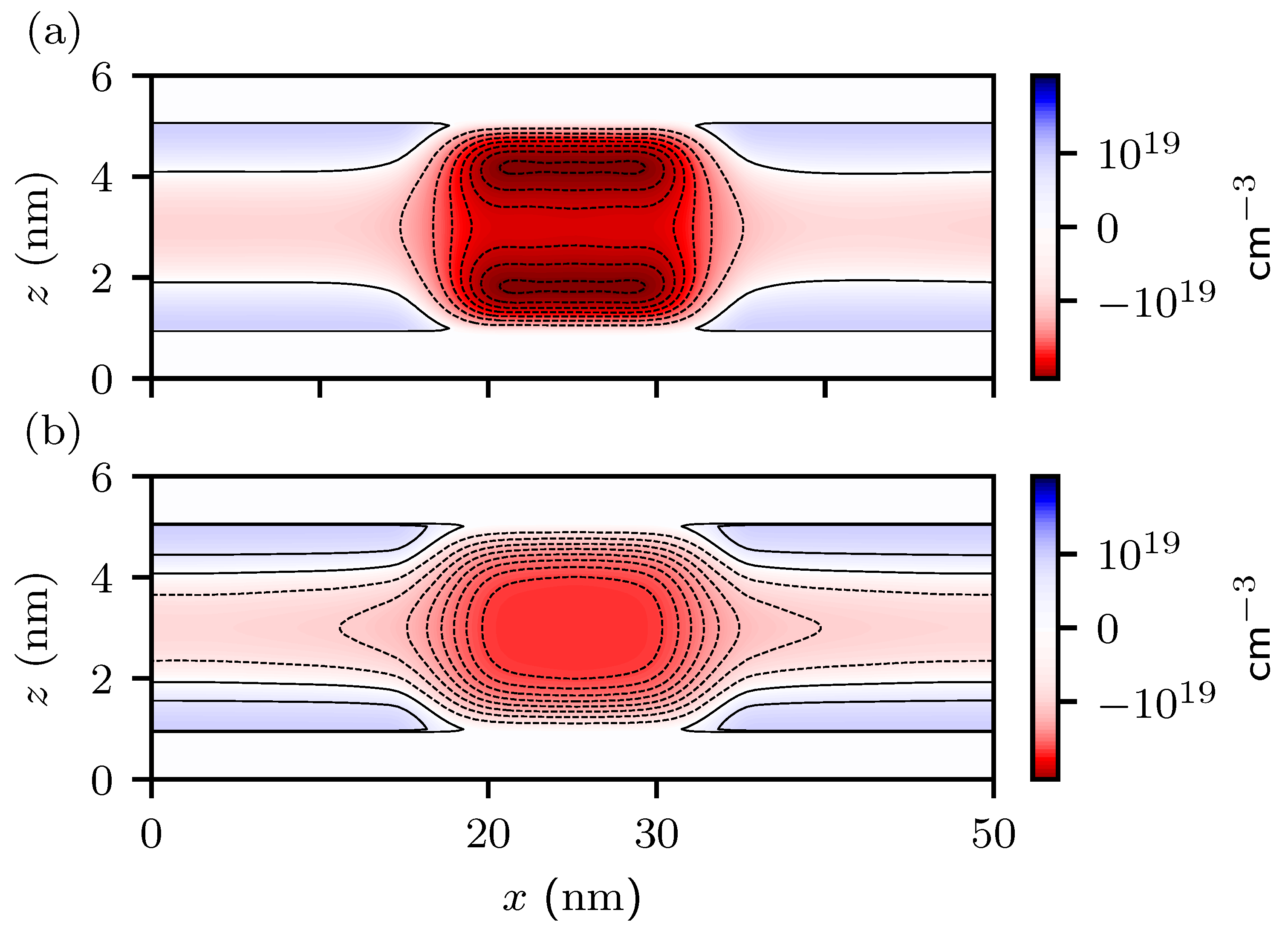
Figure 5 shows the simulated - characteristics of the double-gate nMOS at 10 K and 300 K with equal applied at both gates. Characteristic CMOS behavior is observed with fast switching action represented by a low subthreshold slope (SS) of 64 mV/dec at 300 K, while at 10K the SS drops below this mark as expected. For device operation deep inside saturation, the charge-distribution plot in Figure 6(a) shows the phenomenon of channel inversion (effective reduction of the inversion-layer depth), whereas volume inversion is observed in the linear region of operation (Figure 6(b)). Due to this, the current density takes the shape of a single centered beam close to injection at the source and splits into two beams when flowing through the dual inverted channels at high gate bias, before it finally merges at the drain.
Thus, we show that our QTBM-based quantum transport modeling platform can model 2-D cross-sections of realistic-sized devices and allow in-depth understanding of their electrical behavior by taking into account explicit quantum transport.
4. Summary
In summary, we have built a novel simulation methodology by solving the Schrödinger and Poission equations self-consistently with QTBM boundary conditions on a 2-D device plane. This quantum-transport based methodology can allow more accurate electrical and predictive analyses of realistic semiconductor devices (like FinFET, Gate-all-around and CFET architectures) by taking into account explicit quantum transport while still having manageable computational cost requirement. As an application, we demonstrate the capability of our tool by modeling the electrical behavior of a double-gate MOSFET which essentially acts as a simple investigative study into the behavior of nanosheet-based transistors of current-generation technology nodes.
References
- International Technology Roadmap for Devices and Systems 2017 Edition. https://irds.ieee.org/roadmap-2017.
- Loubet, N.; Hook, T.; Montanini, P.; Yeung, C.W.; Kanakasabapathy, S.; Guillom, M.; Yamashita, T.; Zhang, J.; Miao, X.; Wang, J.; Young, A.; Chao, R.; Kang, M.; Liu, Z.; Fan, S.; Hamieh, B.; Sieg, S.; Mignot, Y.; Xu, W.; Seo, S.C.; Yoo, J.; Mochizuki, S.; Sankarapandian, M.; Kwon, O.; Carr, A.; Greene, A.; Park, Y.; Frougier, J.; Galatage, R.; Bao, R.; Shearer, J.; Conti, R.; Song, H.; Lee, D.; Kong, D.; Xu, Y.; Arceo, A.; Bi, Z.; Xu, P.; Muthinti, R.; Li, J.; Wong, R.; Brown, D.; Oldiges, P.; Robison, R.; Arnold, J.; Felix, N.; Skordas, S.; Gaudiello, J.; Standaert, T.; Jagannathan, H.; Corliss, D.; Na, M.H.; Knorr, A.; Wu, T.; Gupta, D.; Lian, S.; Divakaruni, R.; Gow, T.; Labelle, C.; Lee, S.; Paruchuri, V.; Bu, H.; Khare, M. Stacked nanosheet gate-all-around transistor to enable scaling beyond FinFET. 2017 Symposium on VLSI Technology, 2017, pp. T230–T231. [CrossRef]
- Vyas, P.B.; Zhao, C.; Dag, S.; Pal, A.; Bazizi, E.M.; Ayyagari-Sangamalli, B. Next Generation Gate-all-around Device Design for Continued Scaling Beyond 2 nm Logic. 2023 International Conference on Simulation of Semiconductor Processes and Devices (SISPAD), 2023, pp. 57–60. [CrossRef]
- Vyas, P.B.; Pal, A.; Costrini, G.; Asenov, P.; Mhedhbi, S.; Zhao, C.; Moroz, V.; Colombeau, B.; Haran, B.; Bazizi, E.M.; Ayyagari-Sangamalli, B. Materials to System Co-optimization (MSCO TM ) for SRAM and its application towards Gate-All-Around Technology. 2023 International Conference on Simulation of Semiconductor Processes and Devices (SISPAD), 2023, pp. 53–56. [CrossRef]
- Vyas, P.B.; Pimparkar, N.; Tu, R.; Arfaoui, W.; Bossu, G.; Siddabathula, M.; Lehmann, S.; Goo, J.S.; Icel, A.B. Reliability-Conscious MOSFET Compact Modeling with Focus on the Defect-Screening Effect of Hot-Carrier Injection. 2021 IEEE International Reliability Physics Symposium (IRPS), 2021, pp. 1–4. [CrossRef]
- Weckx, P.; Ryckaert, J.; Litta, E.D.; Yakimets, D.; Matagne, P.; Schuddinck, P.; Jang, D.; Chehab, B.; Baert, R.; Gupta, M.; Oniki, Y.; Ragnarsson, L.A.; Horiguchi, N.; Spessot, A.; Verkest, D. Novel forksheet device architecture as ultimate logic scaling device towards 2nm. 2019 IEEE International Electron Devices Meeting (IEDM), 2019, pp. 36.5.1–36.5.4. [CrossRef]
- Huang, S.; Wu, Z.; Xu, H.; Guo, J.; Xu, L.; Duan, X.; Chen, Q.; Yang, G.; Zhang, Q.; Yin, H.; Wang, L.; Li, L.; Liu, M. Geometric Variability Aware Quantum Potential based Quasi-ballistic Compact Model for Stacked 6 nm-Thick Silicon Nanosheet GAA-FETs. 2021 IEEE International Electron Devices Meeting (IEDM), 2021, pp. 18.5.1–18.5.4. [CrossRef]
- Subramanian, S.; Hosseini, M.; Chiarella, T.; Sarkar, S.; Schuddinck, P.; Chan, B.T.; Radisic, D.; Mannaert, G.; Hikavyy, A.; Rosseel, E.; Sebaai, F.; Peter, A.; Hopf, T.; Morin, P.; Wang, S.; Devriendt, K.; Batuk, D.; Martinez, G.T.; Veloso, A.; Litta, E.D.; Baudot, S.; Siew, Y.K.; Zhou, X.; Briggs, B.; Capogreco, E.; Hung, J.; Koret, R.; Spessot, A.; Ryckaert, J.; Demuynck, S.; Horiguchi, N.; Boemmels, J. First Monolithic Integration of 3D Complementary FET (CFET) on 300mm Wafers. 2020 IEEE Symposium on VLSI Technology, 2020, pp. 1–2. [CrossRef]
- Li, S.; Luo, Y.; Xu, H.; Huo, J.; Di, Z.; Li, Y.; Zhang, Q.; Yin, H.; Wu, Z. Vertically Stacked Nanosheet Number Optimization Strategy for Complementary FET (CFET) Scaling Beyond 2 nm. IEEE Transactions on Electron Devices 2023, 70, 6118–6124. [Google Scholar] [CrossRef]
- Jacoboni, C.; Reggiani, L. The Monte Carlo method for the solution of charge transport in semiconductors with applications to covalent materials. Rev. Mod. Phys. 1983, 55, 645–705. [Google Scholar] [CrossRef]
- Fischetti, M.V.; Laux, S.E. Monte carlo analysis of electron transport in small semiconductor devices including band-structure and space-charge effects. Phys. Rev. B 1988, 38, 9721–9745. [Google Scholar] [CrossRef] [PubMed]
- Sollner, T.C.L.G.; Goodhue, W.D.; Tannenwald, P.E.; Parker, C.D.; Peck, D.D. Resonant tunneling through quantum wells at frequencies up to 2.5 THz. Applied Physics Letters 1983, 43, 588–590. [Google Scholar] [CrossRef]
- Luo, L.F.; Beresford, R.; Wang, W.I. Interband tunneling in polytype GaSb/AlSb/InAs heterostructures. Applied Physics Letters 1989, 55, 2023–2025. [Google Scholar] [CrossRef]
- Naquin, C.; Lee, M.; Edwards, H.; Mathur, G.; Chatterjee, T.; Maggio, K. Negative differential transconductance in silicon quantum well metal-oxide-semiconductor field effect/bipolar hybrid transistors. Applied Physics Letters 2014, 105, 213507. [Google Scholar] [CrossRef]
- Naquin, C.; Lee, M.; Edwards, H.; Mathur, G.; Chatterjee, T.; Maggio, K. Gate length and temperature dependence of negative differential transconductance in silicon quantum well metal-oxide-semiconductor field-effect transistors. Journal of Applied Physics 2015, 118, 124505. [Google Scholar] [CrossRef]
- Wigner, E. On the Quantum Correction For Thermodynamic Equilibrium. Phys. Rev. 1932, 40, 749–759. [Google Scholar] [CrossRef]
- Frensley, W.R. Boundary conditions for open quantum systems driven far from equilibrium. Rev. Mod. Phys. 1990, 62, 745–791. [Google Scholar] [CrossRef]
- de Put, M.L.V.; Sorée, B.; Magnus, W. Efficient solution of the Wigner-Liouville equation using a spectral decomposition of the force field. Journal of Computational Physics 2017, 350, 314–325. [Google Scholar] [CrossRef]
- Kadanoff, L.P.; Baym, G. Quantum Statistical Mechanics; W. A. Benjamin Inc., New York, 1962.
- Keldysh, L.V. Diagram Technique for Nonequilibrium processes. Zh. Eksp. Teor. Fiz. 1964, 47, 1515. [Google Scholar]
- Koswatta, S.O.; Hasan, S.; Lundstrom, M.S.; Anantram, M.P.; Nikonov, D.E. Nonequilibrium Green’s Function Treatment of Phonon Scattering in Carbon-Nanotube Transistors. IEEE Transactions on Electron Devices 2007, 54, 2339–2351. [Google Scholar] [CrossRef]
- Lake, R.; Datta, S. Nonequilibrium Green’s-function method applied to double-barrier resonant-tunneling diodes. Phys. Rev. B 1992, 45, 6670–6685. [Google Scholar] [CrossRef] [PubMed]
- Lake, R.; Klimeck, G.; Bowen, R.C.; Jovanovic, D. Single and multiband modeling of quantum electron transport through layered semiconductor devices. Journal of Applied Physics 1997, 81, 7845–7869. [Google Scholar] [CrossRef]
- Fischetti, M.V. Theory of electron transport in small semiconductor devices using the Pauli master equation. Journal of Applied Physics 1998, 83, 270–291. [Google Scholar] [CrossRef]
- Fischetti, M.V. Master-equation approach to the study of electronic transport in small semiconductor devices. Phys. Rev. B 1999, 59, 4901–4917. [Google Scholar] [CrossRef]
- Vyas, P.B.; Van de Put, M.L.; Fischetti, M.V. Master-Equation Study of Quantum Transport in Realistic Semiconductor Devices Including Electron-Phonon and Surface-Roughness Scattering. Phys. Rev. Appl. 2020, 13, 014067. [Google Scholar] [CrossRef]
- Laux, S.E.; Kumar, A.; Fischetti, M.V. Ballistic FET modeling using QDAME: quantum device analysis by modal evaluation. IEEE Transactions on Nanotechnology 2002, 1, 255–259. [Google Scholar] [CrossRef]
- Vyas, P.B.; Naquin, C.; Edwards, H.; Lee, M.; Vandenberghe, W.G.; Fischetti, M.V. Theoretical simulation of negative differential transconductance in lateral quantum well nMOS devices. Journal of Applied Physics 2017, 121, 044501. [Google Scholar] [CrossRef]
- Vyas, P.B.; Van de Put, M.L.; Fischetti, M.V. Simulation of Quantum Current in Double Gate MOSFETs: Vortices in Electron Transport. 2018 International Conference on Simulation of Semiconductor Processes and Devices (SISPAD), 2018, pp. 1–4. [CrossRef]
- Stern, F. Self-Consistent Results for n-Type Si Inversion Layers. Phys. Rev. B 1972, 5, 4891–4899. [Google Scholar] [CrossRef]
- Vyas, P.B.; Pal, A.; Weeks, S.; Holt, J.; Srivastava, A.K.; Megalini, L.; Krishnan, S.; Chudzik, M.; Bazizi, E.M.; Ayyagari-Sangamalli, B. Modeling of SiC transistor with counter-doped channel. Solid-State Electronics 2023, 200, 108548. [Google Scholar] [CrossRef]
- Lent, C.S.; Kirkner, D.J. The quantum transmitting boundary method. Journal of Applied Physics 1990, 67, 6353–6359. [Google Scholar] [CrossRef]
- Laux, S.E.; Kumar, A.; Fischetti, M.V. Analysis of quantum ballistic electron transport in ultrasmall silicon devices including space-charge and geometric effects. Journal of Applied Physics 2004, 95, 5545–5582. [Google Scholar] [CrossRef]
- Luttinger, J.M.; Kohn, W. Motion of Electrons and Holes in Perturbed Periodic Fields. Phys. Rev. 1955, 97, 869–883. [Google Scholar] [CrossRef]
- Ando, T.; Fowler, A.B.; Stern, F. Electronic properties of two-dimensional systems. Rev. Mod. Phys. 1982, 54, 437–672. [Google Scholar] [CrossRef]
- Saadat, A.; Vyas, P.B.; Put, M.L.V.d.; Fischetti, M.V.; Edwards, H.; Vandenberghe, W.G. Channel Length Scaling Limit for LDMOS Field-Effect Transistors: Semi-classical and Quantum Analysis. 2020 32nd International Symposium on Power Semiconductor Devices and ICs (ISPSD), 2020, pp. 443–446. [CrossRef]
- Abramowitz, M.; Stegun, I.A. Handbook of Mathematical Functions; Dover Publications, Inc., New York, 1972.
- Vyas, P.B.; Van de Putt, M.L.; Fischetti, M.V. Quantum Mechanical Study of Impact of Surface Roughness on Electron Transport in Ultra- Thin Body Silicon FETs. 2018 IEEE 13th Nanotechnology Materials and Devices Conference (NMDC), 2018, pp. 1–4. [CrossRef]
- Zhao, P.; Vyas, P.; McDonnell, S.; Bolshakov-Barrett, P.; Azcatl, A.; Hinkle, C.; Hurley, P.; Wallace, R.; Young, C. Electrical characterization of top-gated molybdenum disulfide metal-oxide-semiconductor capacitors with high-k dielectrics. Microelectronic Engineering 2015, 147, 151–154, Insulating Films on Semiconductors 2015. [Google Scholar] [CrossRef]
Figure 1.
A simplified diagram showing how Dirichlet and Neumann boundary conditions behave at the device-contact interface.
Figure 1.
A simplified diagram showing how Dirichlet and Neumann boundary conditions behave at the device-contact interface.
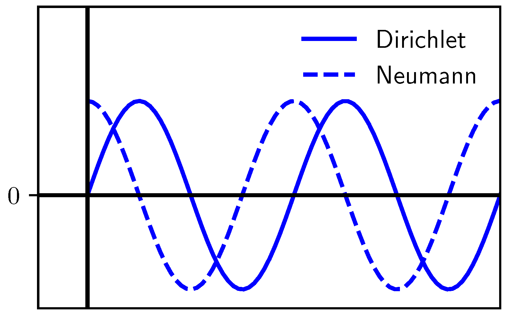
Figure 2.
Representative flow for computing the self-consistent (stead-state solution) of the Schrödinger and Poisson equations.
Figure 2.
Representative flow for computing the self-consistent (stead-state solution) of the Schrödinger and Poisson equations.
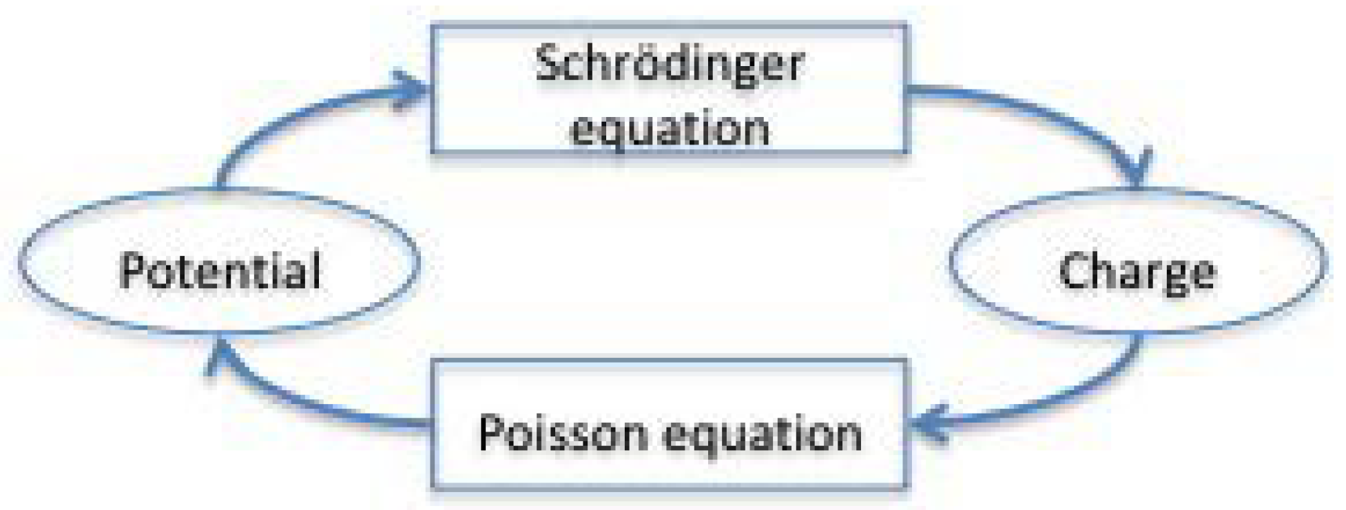
Figure 3.
Schematic illustration showing the implementation of the Quantum Transmitting Boundary Method.
Figure 3.
Schematic illustration showing the implementation of the Quantum Transmitting Boundary Method.
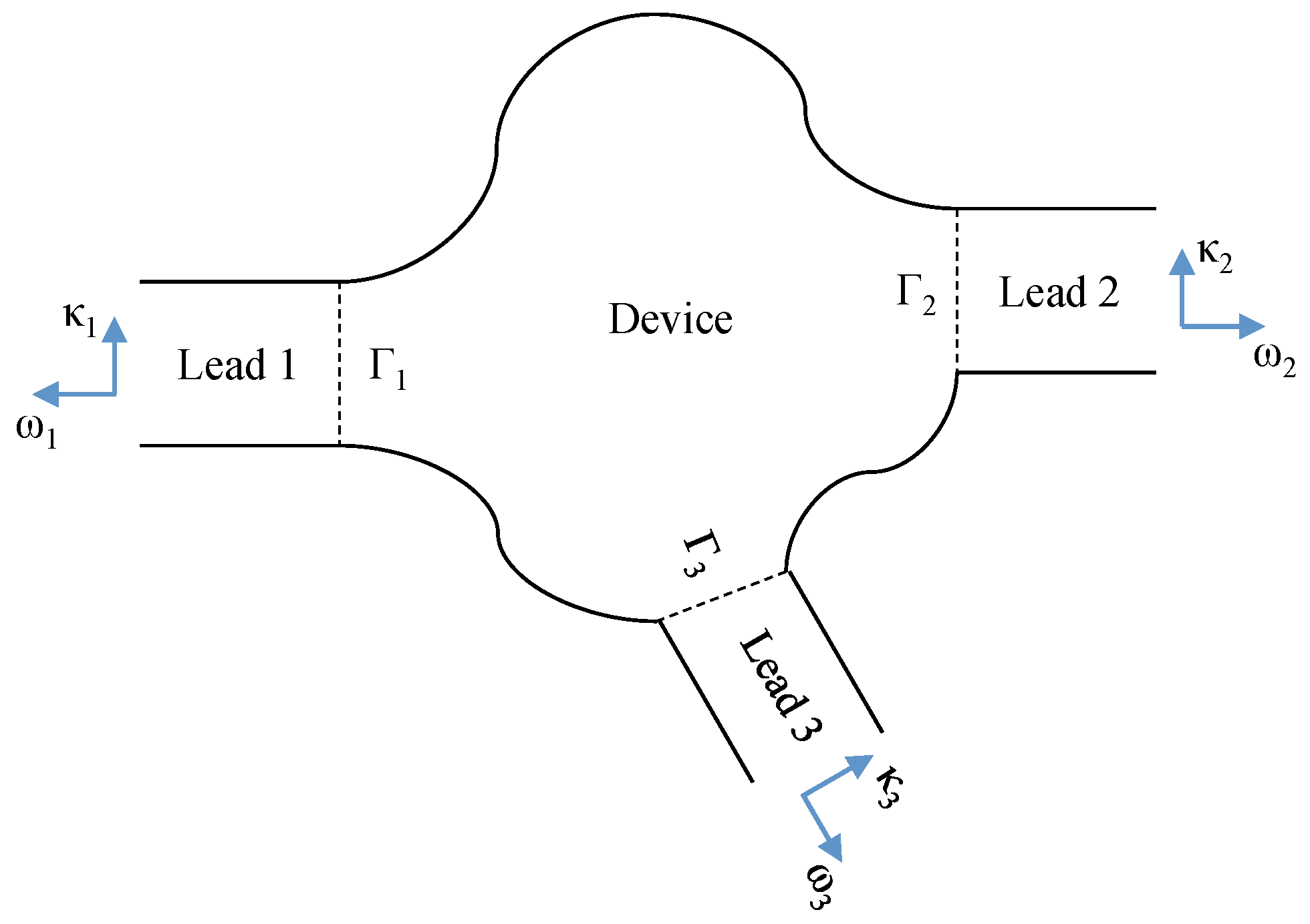
Figure 4.
Active doping profile of the ultra-thin body double-gate nMOS that we investigated. The gate oxide (0.3 nm EOT) and gate terminals are highlighted by the white zones and grey patches, respectively, at the top and bottom.
Figure 4.
Active doping profile of the ultra-thin body double-gate nMOS that we investigated. The gate oxide (0.3 nm EOT) and gate terminals are highlighted by the white zones and grey patches, respectively, at the top and bottom.
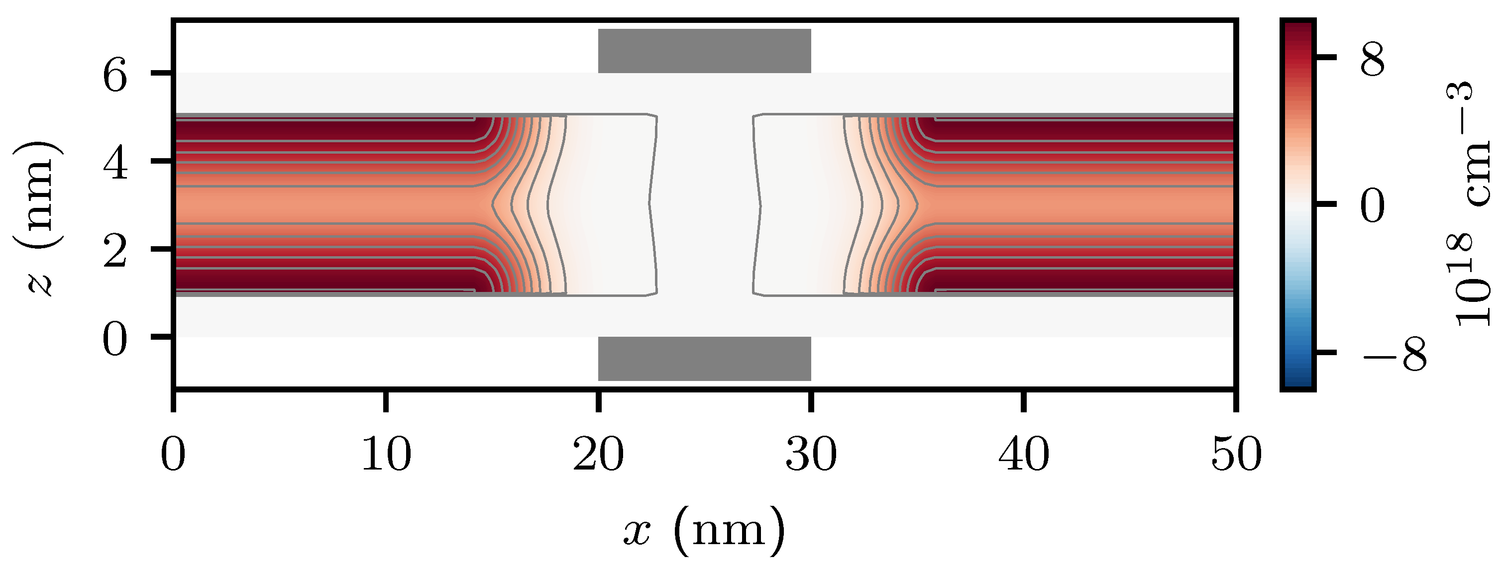
Figure 5.
Simulated transfer characteristics of the 10 nm DG nMOS at 10 K and 300 K. is measured with respect to the flat band voltage of the device. 10 mV. The trend shows realistic transistor behavior with just over 60 mV/V subthreshold slope at 300K and going below that mark at 10K.
Figure 5.
Simulated transfer characteristics of the 10 nm DG nMOS at 10 K and 300 K. is measured with respect to the flat band voltage of the device. 10 mV. The trend shows realistic transistor behavior with just over 60 mV/V subthreshold slope at 300K and going below that mark at 10K.
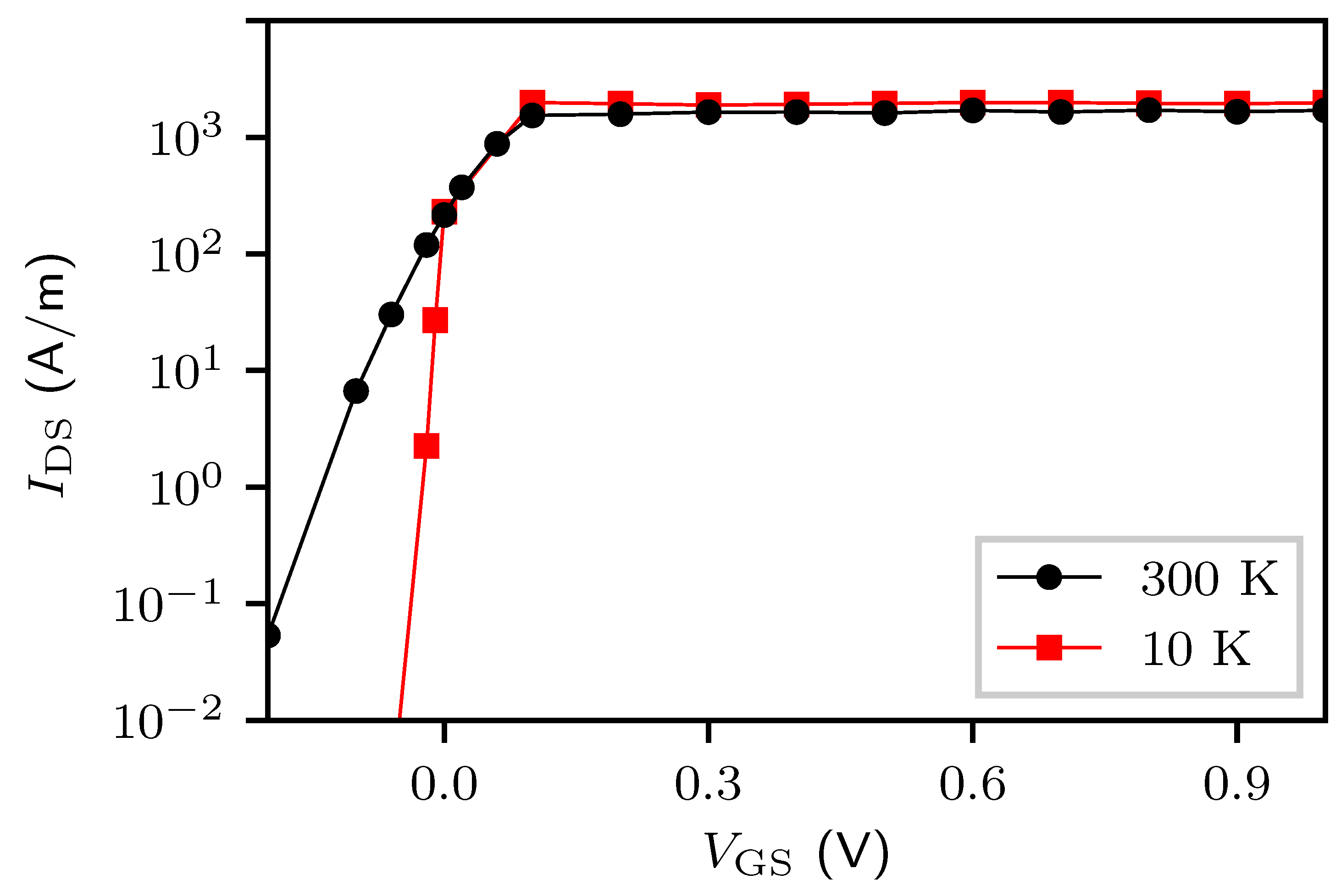
Figure 6.
Electron charge distribution in the simulated double-gate nMOS at 300 K. (a) The darker red regions highlight the presence of two separate inversion channels (surface inversion) close to the gate-semiconductor interfaces deep inside saturation, whereas (b) the linear region of operation exhibits volume inversion. =0.6 V, 10 mV.
Disclaimer/Publisher’s Note: The statements, opinions and data contained in all publications are solely those of the individual author(s) and contributor(s) and not of MDPI and/or the editor(s). MDPI and/or the editor(s) disclaim responsibility for any injury to people or property resulting from any ideas, methods, instructions or products referred to in the content. |
© 2024 by the authors. Licensee MDPI, Basel, Switzerland. This article is an open access article distributed under the terms and conditions of the Creative Commons Attribution (CC BY) license (http://creativecommons.org/licenses/by/4.0/).
Copyright: This open access article is published under a Creative Commons CC BY 4.0 license, which permit the free download, distribution, and reuse, provided that the author and preprint are cited in any reuse.


