Submitted:
19 December 2023
Posted:
19 December 2023
You are already at the latest version
Abstract
Micro-electro-mechanical systems (MEMS) are once proposed in 1970s and evolving rapidly. The current researchers are seeking for better designs and better applications of MEMS actuators. This work presents an electrostatic driven dual-axis scanning micromirror, i.e., two-dimensional (2D) scanning micromirror with a mirror size of 500 μm × 500 μm. The scanning mirror is implemented by using bulk micromachining process on silicon on insulator (SOI) substrate, which is compatible with present complementary metal oxide semiconductor (CMOS) manufacturing technology. The scanning frequencies of the slow and the fast axis are 4.87 kHz and 31.15 kHz, respectively. The impact factors of the dimensions of comb fingers and torsional beams are analyzed and discussed in this study. Under the driving voltage difference of 100 volts and 70 volts, the deviation angle is 4.57° × 13.08°. Therefore, a simple design of a dual-axis MEMS scanning micromirror is proposed, which can be precisely controlled without additional complex sensors or circuits.
Keywords:
MEMS
; electrostatic actuator
; scanning mirror
; dynamical control
1. Introduction
Micro-electro-mechanical systems (MEMS) are once proposed in 1970s and evolving rapidly. Many researchers have analyzed the properties of MEMS microactuators in many aspects, such as reliability and signal-noise ratio (SNR) [1,2,3,4,5,6]. To date, MEMS microactuators have already been used in many aspects. The capability to deflect an incident laser beam at high speed enables MEMS microactuators in laser projection displays [7,8,9,10]. Besides, the advantages of low-cost, better integrated circuit (IC) compatibility and high resolution provide MEMS microactuators with an opportunity in light detection and ranging (LiDAR) fields [11,12,13,14]. The current researchers are seeking for the performance improvement of MEMS microactuators to enable the various applications in micro/nanoscale fields [15,16,17,18,19]. Therefore, the optical MEMS microresonators integrated with MEMS microactuators can be applied as novel chemical sensors [20,21,22].
The actuation mechanisms of MEMS microactuators can be classified into electromagnetic, electrothermal, piezoelectric, and electrostatic actuation forces [23,24,25]. Thanks to the bulk magnets or coils, the electromagnetic actuators can generate great actuation force. However, the electromagnetic actuators require extra magnets to the system, which is bulky and increases the instability as well as reduce the resonant frequency [26,27,28]. As for the piezoelectric actuators, they show advantages in low power consumption, high actuation speed, and large actuation displacement [29,30,31]. However, the piezoelectric materials, e.g., aluminum nitride (AlN), polyvinylidene fluoride (PVDF) are non-compatible with current IC technique. These piezoelectric thin films may limit the performance of the integration of actuators and sensors. For electrothermal actuators, the fabrication is relatively simpler and has better IC compatibility, while the modulation speed or response time is limited that is the main drawback. Therefore, the performance of electrothermal actuator is not good compared to other actuation mechanisms for the use in MEMS scanning micromirror application [32,33,34]. While the electrostatic actuators can meet the demand of modulation speed, response time, and IC compatibility simultaneously. Among the electrostatic actuators, scanning micromirror is the classical sample. One of the scanning micromirror design is used gimbal-less structure to enhance the filling factor of mirror [35]. The fabrication process of scanning micromirror can be completed by using multi-user MEMS processes (MUMPs) and Sandia ultra-planar multilevel MEMS technology-V (SUMMiT-V) processes [36]. However, these fabrication processes are complicated. In this article, we propose a design of dual-axis (2D) electrostatic driving MEMS scanning micromirror. The merits of this design are low power consumption, convenient fabrication, and potential to integrate with other MEMS sensors.
2. Design and method
Figure 1(a) shows the schematic drawing of the proposed 2D scanning micromirror. The micromirror size is an area of 500 μm × 500 μm fixed to a rectangular frame with two pairs of torsion beams. The comb electrodes serve as electrostatic microactuators, which can be divided into fixed combs and movable combs connected to the frame and the micromirror, respectively. By applying the alternative voltages on the combs, the microactuators will generate torques to drive the micromirror to scan along x-axis and y- axis, which are denoted as slow axis and fast axis for x-axis and y- axis, respectively. The overall size of the 2D scanning micromirror is 3 mm × 3 mm, including micromirror, frame, torsion beams, fixed and movable combs, and electrodes. The detail geometric parameters of the 2D scanning micromirror are listed in Table 1.
Figure 1(b) shows the fabrication process flow of the proposed MEMS 2D scanning micromirror. First, a silicon (Si) on insulator (SOI) wafer composed of a device layer, an insulation layer, and a handle layer with 50 μm, 1 μm, and 300 μm in thickness, respectively is prepared. Second, the SOI wafer is etched from the backside using deep reactive etching process (DRIE) to provide a cavity for the rotation of micromirror and frame. Third, the patterns of micromirror, frame, torsion beams, fixed and movable combs, and electrodes are defined using photolithography and DRIE processes subsequently. Finally, the movable structures are released by removing the buried oxide layer using vapor hydrofluoric acid (VHF) etching process. The central structures, i.e., micromirror, torsion beams, movable combs will be sunk owing to the released bulky mass by gravity. That will result in a height difference between the movable and the fixed combs at the initial position as shown in Figure 2(a). When a driving voltage is applied to the electrodes, a voltage potential difference occurs between the movable and the fixed combs, and then there will generate an electrostatic force between comb fingers to drive the combs attracting to each other. Therefore, the micromirror attached to the movable combs will tilt as shown in Figure 2(b). When the driving voltage is applied to the other side of the fixed combs, the electrostatic torque is generated and the micromirror will return to the original position (Figure 2(c)). After that, the micromirror keeps tilting until the rotational inertia and the restoring torque are balanced (Figure 2(d)). Under these steps, the driving voltage is applied again to the initial electrodes to pull the micromirror back to the balanced state and then start another cycle (Figure 2(e)). If the frequency of the applied voltage equals to the eigenfrequency of the micromirror, the scanning angle will come to the largest. Similarly, the frame in fast axis will also tilt because of the electrostatic torque generated by the voltage potential difference between the movable and the fixed combs in slow axis.
Herein, the comb fingers can be regarded as groups of parallel plate capacitors. The torque produced by comb electrodes can be expressed by [37]
where C is the total capacitance generated between the comb fingers, θ is the tilting angle, V is the driving voltage, ε0 is the permittivity of the air, g is the gap between comb fingers, and A denotes the area of the overlapping part. In addition to the torque generated by combs, the dimensions of torsion beams also great influence the vibration modes of the scanning micromirror, which can be expressed by
where Ks is the rotation stiffness of the torsion beam. For a rectangle torsion beam in this study, the rotation stiffness is expressed by Eq. (3) [38].
where G is the shear modulus of the material of the torsion beam. The G value of Si is set as 79.92 GPa. t is the device thickness, w and l are width and length of the torsion beam. The comb finger length increased, and the width and thickness of comb finger decreased could decrease the rotation stiffness and then get a larger tilting angle (θ). While a long and thin torsion beam will reduce the resonant frequency of the scanning micromirror. That will result in the limitation of modulation speed. The worst case is that the system will have a strong impact on the scanning micromirror with an external vibration, and then the mechanical reliability is deteriorated [39,40].
3. Results and discussions
The resonant frequency of the fast axis of the proposed MEMS 2D scanning micromirror is over 30 kHz, which is much faster than the 2D scanning micromirror reported in literature [16]. Moreover, a higher ratio of resonant frequency of fast axis and slow axis is advantageous, leading to a scan pattern with uniform line density. Thus, the scan frequency of slow axis should be relatively low. On the other hand, the drawback is that the MEMS microactuator will be more fragile and more sensitive to the external vibrations. The resonant frequency of slow axis of the proposed MEMS 2D scanning micromirror is around 5 kHz. The modal analysis of the 2D scanning micromirror is presented in Figure 3. In this case, all geometric parameters are listed in Table 1. The 1st scanning mode is at 4.87 kHz and the 2nd resonant mode is named as piston mode at 16.99 kHz as shown in Figure 3(a) and (b), respectively. While the 3rd in-plane vibration mode is at 22.68 kHz as shown in Figure 3(c). When the frequency reaches 31.15 kHz, the mirror will come to 2nd scanning mode, which will be driven by the combs of the slow axis as shown in Figure 3(d). Obviously, the frequencies of the two scanning modes are far from that of the other resonant modes. Therefore, when the micromirror starts to scan, it will not be interfered by the undesired displacement.
To explore the influence degree of comb fingers, Figure 4 shows the resonant frequency of 2D scanning micromirror with different l1 values at slow axis and l2 values at fast axis. All constant geometric parameters are listed in Table 1. In Figure 4(a), the voltage potential difference applied in slow axis is 70 volts to avoid the impact of voltage to the resonance. When l1 = 250 μm, the resonance is at 5.05 kHz and the full width at half maximum (FWHM) value is 2.94 Hz. As l1 value is enlarged to 300 μm, 350 μm, 400 μm, and 450 μm, the resonant frequency will decrease to 5.03 kHz, 5.00 kHz, 4.96 kHz, and 4.93 kHz, respectively. The FWHM values are 3.44 Hz, 2.62 Hz, 3.17 Hz, and 2.74 Hz for l1 = 300 μm, l1 = 350 μm, l1 = 400 μm, and l1 = 450 μm, respectively. In Figure 4(b), the voltage potential difference applied in fast axis is 30 volts. When l2 = 150 μm, the resonance is at 39.55 kHz and the FWHM value is 12.39 Hz. As l2 value is enlarged to 200 μm, 250 μm, 300 μm, and 350 μm, the resonant frequency will decrease to 38.02 kHz, 34.88 kHz, 31.06 kHz, and 27.63 kHz, respectively. The FWHM values are 22.56 Hz, 43.14 Hz, 43.36 Hz and 18.72 Hz for l2 = 200 μm, l2 = 250 μm, l2 = 300 μm, and l2 = 350 μm, respectively.
According to Eq. (1), the torque is impacted by total capacitance generated between the comb fingers. The comb fingers can be regarded as groups of parallel-plate capacitors, the gap between comb fingers will influence on the capacitance and then determine the torque. The relationships between resonances and the g1 and g2 values at the slow axis and the fast axis are plotted in Figure 5(a) and (b), respectively. The driving voltages applied on the slow axis and the fast axis are 70 volts and 30 volts, respectively as listed in Table 1. For the slow axis, when the g1 value is 4 μm, the deviation height of the micromirror is 8.80 μm. As g1 value is enlarged, the torque decreases and the deviation height declines gradually until 1.58 μm at g1 = 7 μm. Additionally, as the gap becomes wide, under the circumstance of constant numbers of comb fingers (n1), the whole electrostatic actuator will become larger and heavier. Therefore, the resonant frequency of the scanning micromirror goes down from 4.87 kHz to 4.85 kHz as shown in Figure 5(a). In Figure 5(b), when g2 value is 6 μm for the fast axis, a deviation height of 21.07 μm is achieved at 31.82 kHz. As g2 value increases, the deviation height decreases more sharply compared to that at the slow axis. When g2 value equals to 9 μm, the deviation height is just 0.64 μm at the resonance at 30.83 kHz. Thus, narrower gaps lead to larger deviation height under the same voltage difference. While small gap values will enlarge the aspect ratio, which lead to difficulties for fabrication progress. Therefore, a compromise must be taken between deviation height and process simplicity in the design.
Figure 6(a) and (b) show the influences of the torsion beam dimensions to the 2D scanning micromirror at slow axis and fast axis, respectively. For the slow axis in Figure 6(a), when the torsion beam dimension is 800 μm × 10 μm, the torsion beam is relatively the most flexible and the resonant frequency is only at 0.80 kHz. It means that the micromirror can be driven at a low applied voltage. On the other hand, the restoration time of the slow axis is long, that results in the limitation of modulation speed. The worst case is that the whole system is fragile and sensitive to external vibrations. When the torsion beam goes shorter and thicker, it becomes harder, and the resonant frequency goes higher. For example, the torsion beam dimension is 100 μm × 60 μm, the torsion beam at slow axis is hardest and the resonant frequency is at 17.85 kHz. Additionally, the torsion beam length has more significant influence only when the torsion beam width becomes wwider until wt1 = 50 μm or 60 μm. For the fast axis in Figure 6(b), when the torsion beam dimension varies from 800 μm × 10 μm to 100 μm × 60 μm, the resonant frequency covers a larger range from 5.42 kHz to 39.57 kHz. The torsion beam length has more significant influence at wt2 = 20 μm or 30 μm. Though a higher ratio of fast axis and slow axis frequency benefits the scanning performance, it should also pay attention to the undesired resonant modes as the discussions in Figure 3. It should be noted that the eigenfrequency of the comb fingers is at around 38.00 kHz. As a result, if the resonant frequency is set improperly, the comb fingers will also vibrate and stick to each other. This issue is the key for the design of MEMS scanning micromirror.
Figure 7 shows the relationships of the driving voltages to the deviation angles for fast and slow axes. According to Eq. (1) and (2), the deviation angle should be proportional to the square of voltage difference. For the slow axis, there is an initial deviation angle of 0.23° at V1 = 0 volt. As V1 value increases to 100 volts, the deviation angle is larger until 4.57° simultaneously. The relationship between deviation angle and voltage difference is y = 0.0008x2 - 0.04x + 0.6243 by using the binomial fitting method as the dot lines plotted in Figure 7. Herein, the correlation coefficient is 0.9759. For the fast axis, the deviation angle of 0.63° at V2 = 0 volt. As V2 value increases, the deviation angle is largest as 13.08° at V2 = 70 volts. The relationship between deviation angles and voltage differences is y = 0.0035x2 - 0.0957x + 1.2938. The corresponding correlation coefficient is 0.9849. These results show the design of the proposed MEMS scanning micromirror possesses high linear characteristic between deviation angles and voltage differences.
4. Conclusion
In conclusion, we present a design and analysis of a dual-axis (2D) electrostatic driving scanning micromirror. The scanning micromirror is stabilized by frame microstructures and supported by two groups of torsion beams which anchored to the substrate. After the input signal of driving voltage at specific frequency is applied to the combs at the slow axis and the fast axis, respectively, the micromirror is driven and starts scanning. The resonant frequency of the scanning micromirror along the two axes is 4.88 kHz and 31.15 kHz. As the micromirror size is 500 μm × 500 μm, the proposed design is one of the best compromise methods of high ratio of the dual-axis scanning frequency and the stability. It can avoid the undesired resonances. Furthermore, the impact of the comb fingers as well as the torsion beams along two axes is discussed. This study verifies the square relationship between the driving voltages and the deviation angles at resonances. It is expected to integrate with other MEMS sensors and has better prospects if a larger scanning angle can be obtained at a lower voltage. The proposed MEMS 2D scanning micromirror possesses the merits of IC compatibility, low cost, low power consummation, and easy integration.
Data Availability Statement
Data availabilities are requested by authors.
Acknowledgments
The authors acknowledge the financial support from Guangzhou Basic and Applied Basic Research Project (202201011829) and the State Key Laboratory of Optoelectronic Materials and Technologies of Sun Yat-Sen University for the use of experimental equipment.
Disclosures
The authors declare no conflicts of interest.
References
- W. M. Miller, “Reliability: A Hidden Barrier to Successful Commercialization of MEMS”, Micromachine Devices, 1-4 (1997).
- Y. Hu, X. Shen, Y. Zhang, Z. Wang, and X. Chen, “Research Reviews and Prospects of MEMS Reliability”, Integrated Ferroelectrics, 152(1), 8-21 (2014). [CrossRef]
- F. Mohd-Yasin, D. J. Nagel, and C. E. Korman, “Noise in MEMS”, Measurement Science and Technology, 21(1), 012001 (2010). [CrossRef]
- X. Y. Fang, C. C. Liu, X. Y. Li, J. H. Wu, K. M. Hu, and W. M. Zhang, “Evaluation of Residual Stress in MEMS Micromirror Die Surface Mounting Process and Shock Destructive Reliability Test”, IEEE Sensors Journal, 23(14), 15461-15468 (2023). [CrossRef]
- X. Y. Fang, X. Y. Li, K. M. Hu, G. Yan, J. H. Wu, and W. M. Zhang, “Destructive Reliability Analysis of Electromagnetic MEMS Micromirror Under Vibration Environment”, IEEE Journal of Quantum Electronics, 28(5), 2022. [CrossRef]
- H. An, E. E. Langas, and A. S. Gill, “Effect of Scanning Speed, Scanning Pattern, and Tip Size on the Accuracy of Intraoral Digital Scans”, The Journal of Prosthetic Dentistry, 2022. [CrossRef]
- U. Hofmann, S. Muehlmann, M. Witt, K. Doerschel, R. Schuetz, and B. Wagner, “Electrostatically Driven Micromirrors for A Miniaturized Confocal Laser Scanning Microscope”, Proceedings of SPIE, 29-38 (1999). [CrossRef]
- U. Hofmann, J. Janes, and H.-J. Quenzer, “High-Q MEMS Resonators for Laser Beam Scanning Displays”, Micromachines, 3, 509-528 (2012). [CrossRef]
- B. G. Cho, H. S. Tae, D. H. Lee, and S. Chein, “A new overlap-scan circuit for high speed and low data voltage in plasma-TV”, IEEE Transaction on Consumer Electronics, 51(4), 1218-1222 (2022). [CrossRef]
- Y.-H. Seo, K. Hwang, H. Kim, and K.-H. Jeong, “Scanning MEMS Mirror for High Definition and High Frame Rate Lissajous Patterns”, Micromachines, 10(1), 2019. [CrossRef]
- D. Yang, Y. Liu, Q. Chen, M. Chen, S. Zhan, N.-K. Cheung, H.-Y. Chan, Z. Wang, and W. J. Li, “Development of the High Angular Resolution 360° LiDAR based on Scanning MEMS Mirror”, Scientific Reports, 13, 1540 (2023). [CrossRef]
- W. C. Stone, M. Juberts, N. Dagalakis, J. A. Stone Jr., and J. J. Gorman, “Performance Analysis of Next-Generation LADAR for Manufacturing, Construction, and Mobility”, NIST Interagency or Internal Reports, 7117 (2004). [CrossRef]
- F. Xu, D. Qiao, C. Xia, X. Song, and Y. He, “Fast Synchronization Method of Comb-Actuated MEMS Mirror Pair for LiDAR Application”, Micromachines, 12(11), 2021. [CrossRef]
- Q. Li, Y. Zhang, R. Fan, Y. Wang, Y. Wang, and C. Wang, “MEMS mirror based omnidirectional scanning for LiDAR optical systems”, Optics and Lasers in Engineering, 158, 10178 (2022). [CrossRef]
- Z. Ren, Y. Chang, Y. Ma, K. Shih, B. Dong, and C. Lee, “Leveraging of MEMS Technologies for Optical Metamaterials Applications”, Advanced Optical Materials, 8(3) (2020). [CrossRef]
- W. M. Zhu, A. Q. Liu, X. M. Zhang, D. P. Tsai, T. Bourouina, J. H. Teng, X. H. Zhang, H. C. Guo, H. Tanoto, T. Mei, G. Q. Lo, and D. L. Kwong, “Switchable Magnetic Metamaterials Using Micromachining Processes”, Advanced Materials, 23(15), 1792-1796 (2011). [CrossRef]
- S. Chen, S. F. Tan, H. Singh, L. Liu, M. Etienne, and P. S. Lee, “Functionalized MXene Films with Substantially Improved Low-voltage Actuation”, Advanced Materials, e2307045 (2023). [CrossRef]
- H. Tao, A. C. Strikwerda, K. Fan, W. J. Padilla, X. Zhang, and R. D. Averitt, “Reconfigurable Terahertz Metamaterials”, Physical Review Letters, 103, 147401 (2009). [CrossRef]
- P. F. McManamon, P. J. Bos, M. J. Escuti, J. Heikenfeld, S. Serati, H. K. Xie, and E. A. Watson, “A Review of Phased Array Steering for Narrow-Band Electrooptical Systems”, Proceedings of the IEEE, 97(6), 1078-1096 (2009). [CrossRef]
- X. Hu, G. Q. Xu, L. Wen, H. C. Wang, Y. C. Zhao, Y. X. Zhang D.R.S. Cumming, and Q. Chen, “Metamaterial Absorber Integrated Microfluidic Terahertz Sensors”, Laser & Photonics Reviews, 10(6), 962-969 (2016). [CrossRef]
- B. Appasani, A. Srinivasulu, and C. Ravariu, “A high Q terahertz metamaterial absorber using concentric elliptical ring resonators for harmful gas sensing applications”, Defence Technology, 22, 69-73 (2023). [CrossRef]
- X. Xu, D. Zheng, and Y.-S. Lin, “Electric Split-Ring Metamaterial Based Microfluidic Chip with Multi-Resonances for Microparticle Trapping and Chemical Sensing Applications”, Journal of Colloid Interface Science, 642, 462-469 (2023). [CrossRef]
- D. Wang, C. Watkins, and H. Xie, “MEMS Mirrors for LiDAR: A Review”, Micromachines, 11, 456 (2020). [CrossRef]
- J. Wang, G. Zhang, and Z. You, “Improved Sampling Scheme for LiDAR in Lissajous Scanning Mode”, Microsystems & Nanoengineering, 8(1), 64 (2022). [CrossRef]
- J. Raj, F. H. Hashim, A. B. Huddin, M. F. Ibrahim, and A. Hussain, “A Survey on LiDAR Scanning Mechanisms”, Electronics, 9(5), 741 (2020). [CrossRef]
- T. Iseki, M. Okumura, and T. Sugawara, “Two-Dimensionally Deflecting Mirror Using Electromagnetic Actuation”, Optical Review, 13, 189-194 (2006). [CrossRef]
- C. Ataman, S. Lani, W. Noell, and N. De Rooij, “A Dual-Axis Pointing Mirror with Moving-Magnet Actuation”, Journal of Micromechanics and Microengineering, 23, 25002 (2012). [CrossRef]
- J. Yunas, B. Mulyanti, I. Hamidah, M. Mohd Said, R. E. Pawinanto, W. A. F. W. Ali, A. Subandi, A. A. Hamzah, R. Latif, and B. Yeop Majlis, “Polymer-Based MEMS Electromagnetic Actuator for Biomedical Application: A Review”, Polymers, 12(5), 1184 (2020). [CrossRef]
- Y. Zhu, W. Liu, K. Jia, W. Liao, and H. Xie, “A Piezoelectric Unimorph Actuator Based Tip-Tilt-Piston Micromirror with High Fill Factor and Small Tilt and Lateral Shift”, Sensors and Actuators A: Physical, 167, 495-501 (2011). [CrossRef]
- W. Liu, Y. Zhu, K. Jia, W. Liao, Y. Tang, B. Wang, and H. Xie, “A Tip-Tilt-Piston Micromirror with a Double S-shaped Unimorph Piezoelectric Actuator”, Sensors and Actuators A: Physical, 193, 121-128 (2013). [CrossRef]
- S. Mohith, A. R. Upadhya, K. P. Navin, S. M. Kulkarni, and M. Rao, “Recent Trends in Piezoelectric Actuators for Precision Motion and Their Applications: A Review”, Smart Materials and Structures, 30(1), 013002 (2021). [CrossRef]
- H. Tao, A. C. Strikwerda, K. Fan, W. J. Padilla, X. Zhang, and R. D. Averitt, “Reconfigurable Terahertz Metamaterials”, Physical Review Letters, 103, 147401 (2009). [CrossRef]
- Y. Tang, J. H. Li, L. X. Xu, J. B. Lee, and H. K. Xie, “Review of Electrothermal Micromirrors”, Micromachines, 13(3), 429 (2022). [CrossRef]
- Potekhina, and C. Wang, “Review of Electrothermal Actuators and Applications”, Actuators, 8(4), 69 (2020). [CrossRef]
- J. Tsai, and M. C. Wu, “Design, Fabrication, and Characterization of a High Fill-Factor, Large Scan-Angle, Two-Axis Scanner Array Driven by a Leverage Mechanism”, Journal of Microelectromechanical System, 15(5), 1209-1213 (2006). [CrossRef]
- B. Sargent, R. Harbourne, N. G. Moreau, T. Sukal-Moulton, M. Tovin, J. L. Cameron, R. D. Stevenson, I. Novak, and J. Heathcock, “Research Summit V: Optimizing Transitions from Infancy to Early Adulthood in Children with Neuromotor Conditions”, Pediatric Physical Therapy, 34(3), 411-417 (2022). [CrossRef]
- D. Hah, P. R. Patterson, H. D. Nguyen, H. Toshiyoshi, and M. C. Wu, “Theory and Experiments of Angular Vertical Comb-Drive Actuators for Scanning Micro-mirrors”, IEEE Journal of Selected Topics in Quantum Electronics, 10 (3), 505-513 (2004). [CrossRef]
- T. Izawa, T. Sasaki, and K. Hane, “Scanning Micro-Mirror with an Electrostatic Spring for Compensation of Hard-Spring Nonlinearity”, Micromachines, 8(8), (2017). [CrossRef]
- D. Brunner, H. W. Yoo, and G. Schitter, “Linear Modeling and Control of Comb-Actuated Resonant MEMS Mirror With Nonlinear Dynamics”, IEEE Transactions on Industrial Electronics, 68(4), 3315-3323 (2021). [CrossRef]
- T. Tsuchiya, “Tensile testing of silicon thin films”, Deep Underground Science and Engineering, 665-674 (2005). [CrossRef]
Figure 1.
(a) Schematic drawing and (b) fabrication process flow of the proposed 2D scanning micromirror.
Figure 1.
(a) Schematic drawing and (b) fabrication process flow of the proposed 2D scanning micromirror.
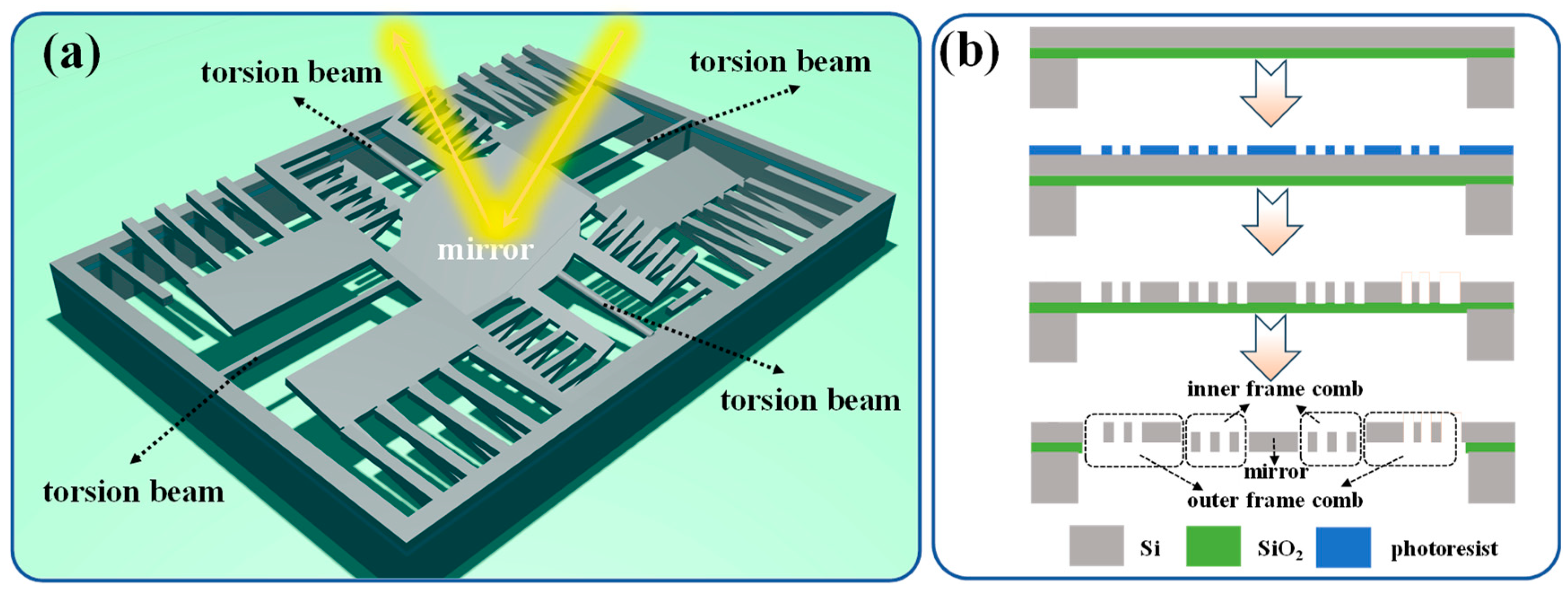
Figure 2.
Cross-sectional views of the scanning micromirror tilting in a cycle.
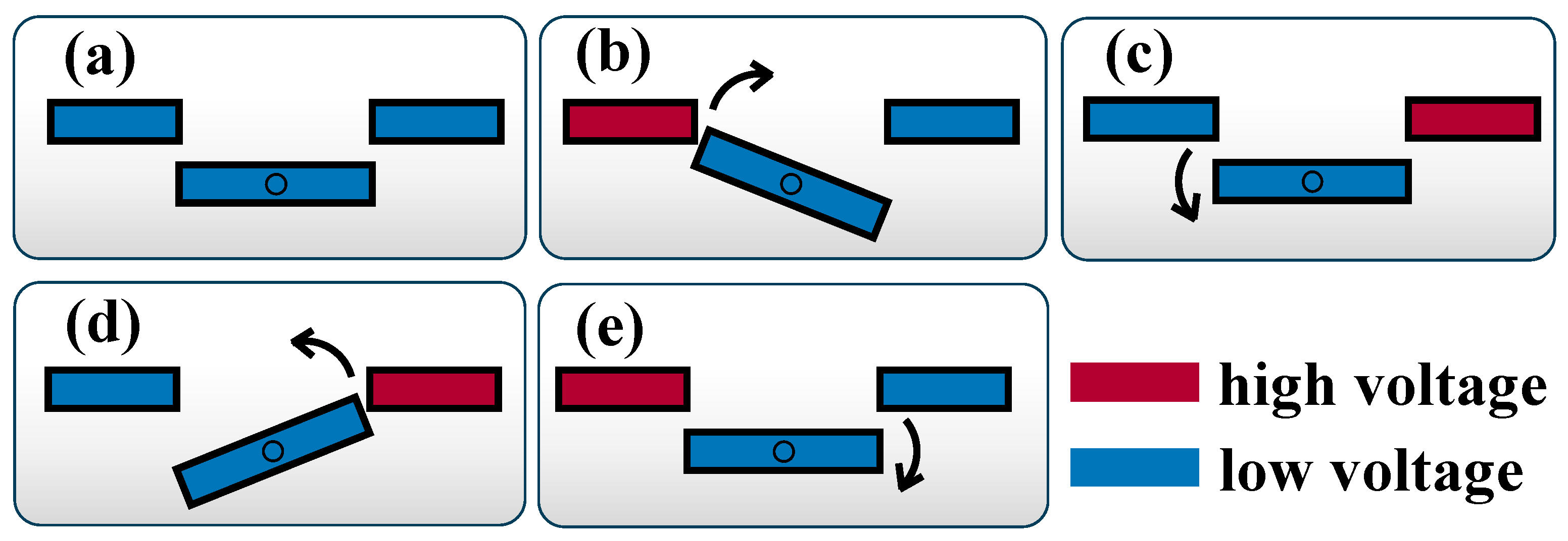
Figure 3.
Four resonant modes of the proposed 2D scanning micromirror. They are (a) 1st scanning mode at 4.87 kHz, (b) piston mode at 16.99 kHz, (c) in-plane vibration mode at 22.68 kHz, and (d) 2nd scanning mode at 31.15 kHz, respectively.
Figure 3.
Four resonant modes of the proposed 2D scanning micromirror. They are (a) 1st scanning mode at 4.87 kHz, (b) piston mode at 16.99 kHz, (c) in-plane vibration mode at 22.68 kHz, and (d) 2nd scanning mode at 31.15 kHz, respectively.
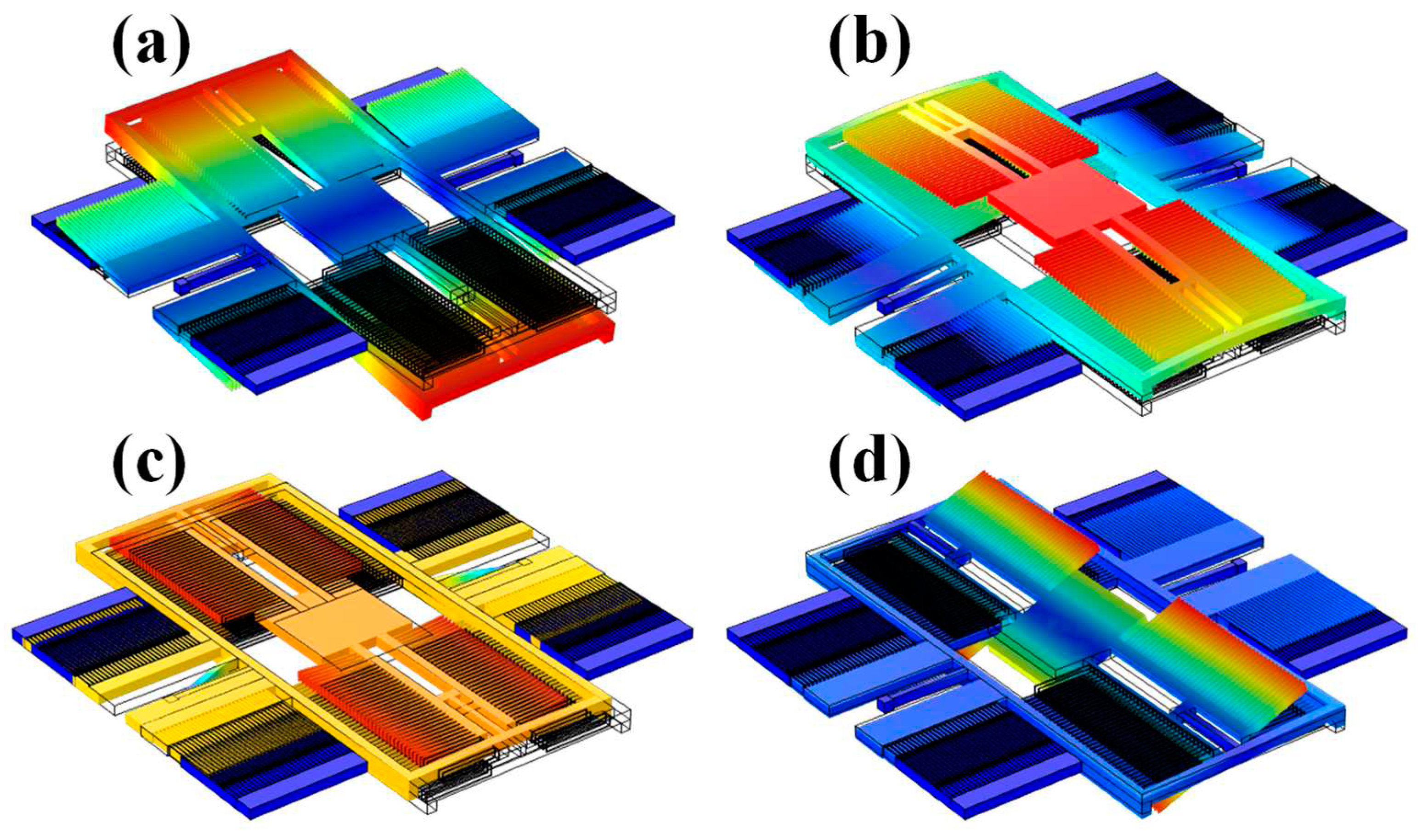
Figure 4.
The resonant frequency of 2D scanning micromirror with different (a) l1 values at the slow axis and (a) l2 values at the fast axis.
Figure 4.
The resonant frequency of 2D scanning micromirror with different (a) l1 values at the slow axis and (a) l2 values at the fast axis.
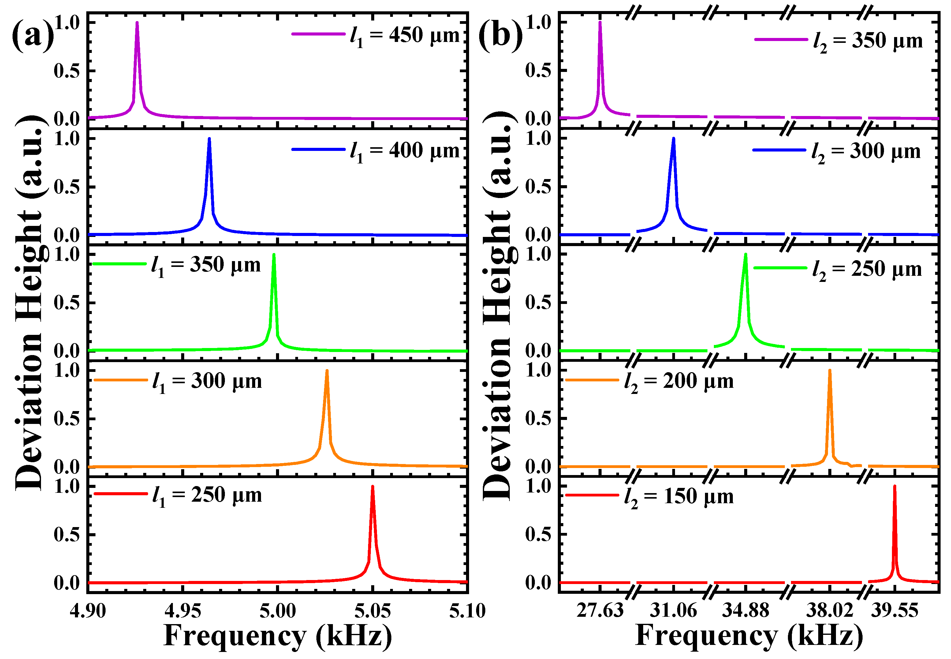
Figure 5.
The relationships between resonances and the g1 and g2 values at (a) the slow axis and (b) the fast axis, respectively.
Figure 5.
The relationships between resonances and the g1 and g2 values at (a) the slow axis and (b) the fast axis, respectively.
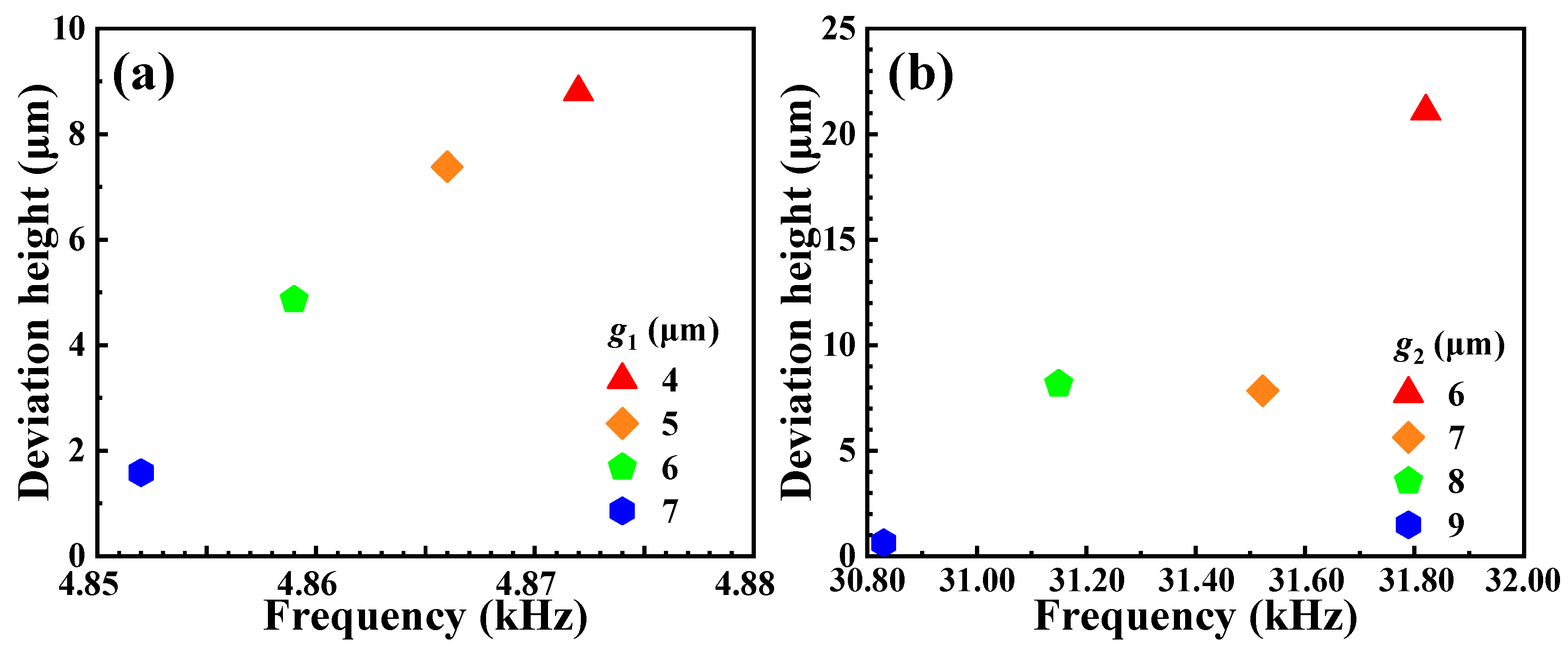
Figure 6.
The influences of the torsion beam dimension to the 2D scanning micromirror at (a) the slow axis and (b) the fast axis, respectively.
Figure 6.
The influences of the torsion beam dimension to the 2D scanning micromirror at (a) the slow axis and (b) the fast axis, respectively.
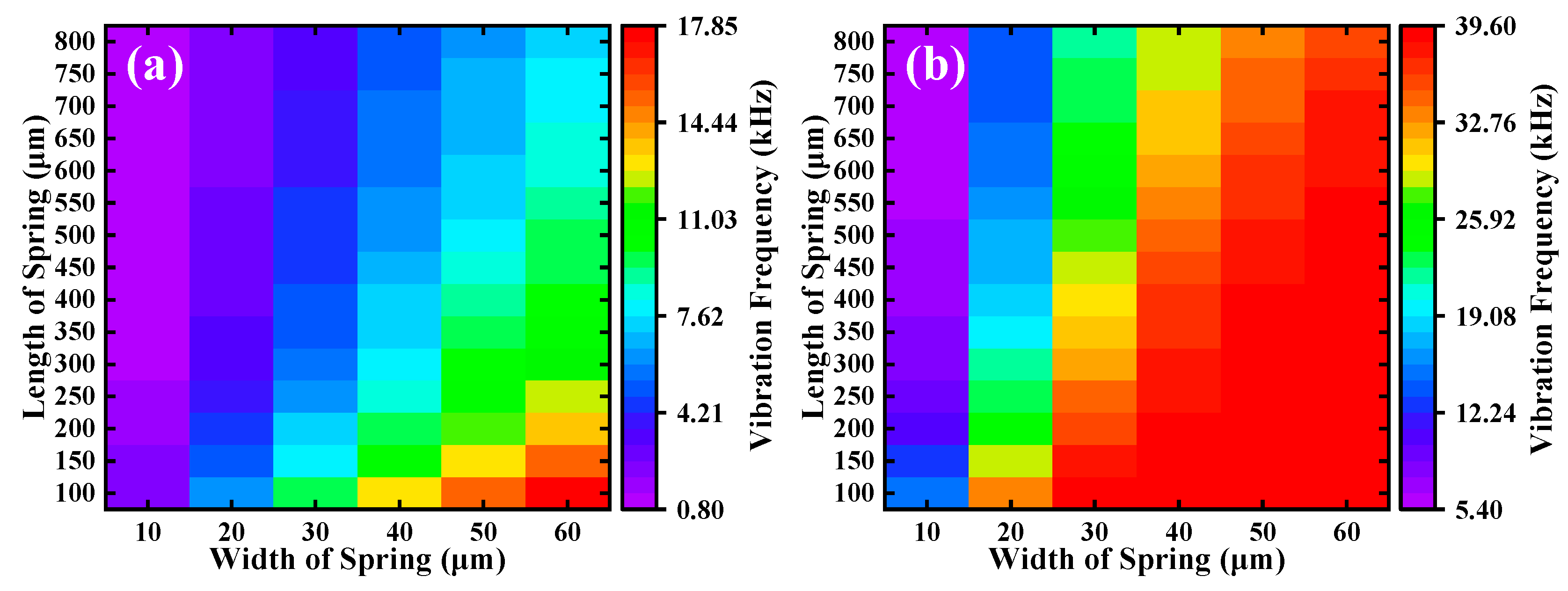
Figure 7.
The relationships of the driving voltages to the deviation angles for the fast and the slow axes.
Figure 7.
The relationships of the driving voltages to the deviation angles for the fast and the slow axes.
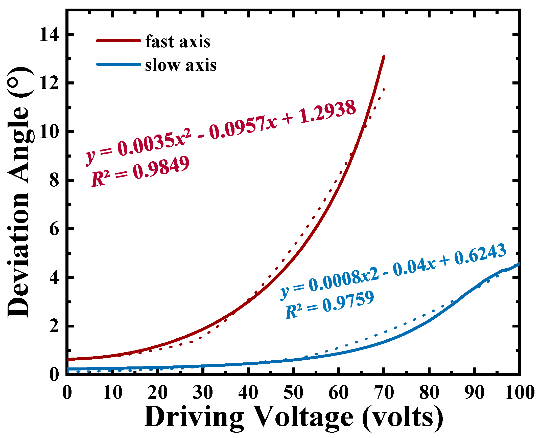

Table 1.
D scanning micromirror.
| parameter | value |
|---|---|
| mirror size | 500 μm × 500 μm |
| length of torsion beam in slow axis, lt1 | 400 μm |
| width of torsion beam in slow axis, wt1 | 30 μm |
| length of torsion beam in fast axis, lt2 | 350 μm |
| Width of torsion beam in fast axis, lt2 | 30 μm |
| length of fingers in slow axis, l1 | 400 μm |
| width of fingers in slow axis, w1 | 5 μm |
| gap between fingers in slow axis, g1 | 5 μm |
| overlapping length of slow axis, lo1 | 300 μm |
| number of fingers in slow axis, n1 | 30 × 4 |
| length of fingers in fast axis, l2 | 300 μm |
| width of fingers in fast axis, w2 | 5 μm |
| gap between fingers in fast axis, g2 | 8 μm |
| overlapping length of fast axis, lo2 | 250 μm |
| number of fingers in fast axis, n2 | 34 × 4 |
| voltage potential difference between slow combs, V 1 | 70 volts |
| voltage potential difference between fast combs, V 2 | 30 volts |
| thickness of the scanning micromirror, t | 50 μm |
Disclaimer/Publisher’s Note: The statements, opinions and data contained in all publications are solely those of the individual author(s) and contributor(s) and not of MDPI and/or the editor(s). MDPI and/or the editor(s) disclaim responsibility for any injury to people or property resulting from any ideas, methods, instructions or products referred to in the content. |
© 2023 by the authors. Licensee MDPI, Basel, Switzerland. This article is an open access article distributed under the terms and conditions of the Creative Commons Attribution (CC BY) license (http://creativecommons.org/licenses/by/4.0/).
Copyright: This open access article is published under a Creative Commons CC BY 4.0 license, which permit the free download, distribution, and reuse, provided that the author and preprint are cited in any reuse.


