Submitted:
19 November 2023
Posted:
20 November 2023
You are already at the latest version
Abstract
A tunable near-infrared surface plasmon resonance (SPR) biosensor based on gate-controlled graphene plasmons is investigated theoretically. The novel characteristics of chemical potential sensing make the proposed sensor promising in the application of ultra-sensitive and highly specific biosensing technology. The sensitivity of chemical potential sensing in wavelength interrogation mode can be calculated to be 1.5, 1.89, 2.29, 3.21, 3.73 and 4.68 nm/meV respectively at the central wavelength of 1100, 1200, 1310, 1550, 1700 and 1900 nm. The much smaller full width half maximum (FWHMs) comparing with that of 2D nanomaterial-enhanced metal SPR sensors indicates higher figure of merit. The sensitivity of chemical potential sensing in gate voltage interrogation mode also can be calculated to be 156.9822, 143.6147, 131.0779, 111.0351, 101.3415 and 90.6038 mV/meV respectively at the incident wavelength of 1100, 1200, 1310, 1550, 1700 and 1900 nm. It can be estimated theoretically that the limit of detection (LOD) in DNA sensing of the proposed sensor can reach femtomolar level and even attomolar level, comparable to and even lower than that of 2D nanomaterial-enhanced metal SPR sensors with AuNPs as a sensitivity enhancement strategy. The feasibility of preparation and operation of this new concept SPR biosensor is also analyzed and discussed.
Keywords:
surface plasmon resonance biosensor
; graphene plasmon
; chemical potential sensing
1. Introduction
SPR biosensors are powerful optical sensors for probing interactions between an analyte in solution and a biomolecular recognition element immobilized on the SPR sensor surface. In noble metal-based SPR biosensors, a surface plasmon wave (SPW) that propagating along the surface of the metal can be excited by an incident light (through prism-, waveguide-, or grating-coupling) if the component of its wave vector that is parallel to the metal surface matches that of the SPW [1]. When the target bio molecules (antigens, target DNAs, etc.) in the aqueous solution are captured by specific biomolecule recognition elements (antibodies, probe DNAs, etc.) immobilized on the SPR sensor surface, the binding-induced refractive index change in the analyte layer will cause the change of the propagation constant of SPW that propagate along the interface between the metal and the dielectric (analyte layer). The characteristics of a light wave, such as amplitude, phase, polarization, and spectral distribution consequently changes due to its interaction with the SPW. By measuring the change of one of the light wave characteristics (through angle, wavelength, intensity, phase, or polarization interrogation), the binding-induced refractive index change can be determined. However, the weak adhesion between metal surfaces and biomolecule recognition elements limits the sensitivity of the SPR biological sensors. In the last decade, the use of graphene, black phosphorose (BP), transition metal dichalcogenides (TMDCs) and other 2D materials, to enhance the performance of SPR biological sensors has attracted wide attentions [2]. Graphene-on-gold structure was firstly considered and its enhanced sensitivity was theoretically demonstrated [3]. Some more complex 2D material heterostructures such as graphene-BP-metal [4], graphene-WS2-metal [5], graphene-MoS2-metal [6], WSe2-WS2-MoS2-graphene-metal [7], etc, were also considered. The enhancement of sensitivity of 2D material-enhanced metal SPR sensors was also demonstrated experimentally through their applications in protein detection [8,9,10], glucose detection [11], immunoassay [12,13], and DNA sensing [14,15,16,17,18]. Despite the sensitivity of noble metal-based SPR sensors has been greatly improved by using various sensitization strategies, they still have some inherent disadvantages to overcome: (1) The refractive index sensing property of noble metal-based SPR sensor makes it easy to be interfered with and has poor specificity [1]. (2) Many 2D material-enhanced metal SPR biosensors still need to rely on the synergistic effect of the localized SPR effect of metallic nanoparticles [19] to achieve high sensitivity, which increases the complexity, expenditure, and uncertainty of the sensors. (3) The operating wavelengths of noble metal-based SPR sensors are limited to visible spectrum and near-infrared spectrum very close to visible waveband, which is usually not tunable.
Plasmons supported by graphene, a 2D semiconductor, have a different characteristic than those in noble metals: they can be tuned by gating or doping [20,21]. Inspired by terahertz plasmon studies in 2D traditional electron gas system, the studies of graphene plasmons in the early stage mainly focuses on the terahertz to mid-infrared waveband, such as localized plasmons in graphene nanostructures [22,23,24,25], propagating plasmons excited by metallic tip [26,27], etc. Based on the relation as ωp∝(μc/D)1/2, where ωp, μc, and D represent frequency of plasmon resonance in graphene nanostructure, chemical potential (Fermi level) of graphene, and characteristic dimension of graphene nanostructure respectively, a thinking way for extending the study of graphene plasmon to near-IR and even visible waveband is constantly reducing the size of the graphene nanostructure [28,29]. Until now, the shortest wavelength of the localized graphene plasmon was observed at 2 μm in 18 nm-diameter graphene nanodisks [30]. However, the challenges this approach (further reduction in size) has to face are more complex preparation processes, reduced carrier mobility (~10 times or more lower than those of large 2D graphene sheets) [31,32], and increased defects related to the formation of graphene nanostructure edges [30]. Graphene plasmons have strong spatial light confinement (two orders [39] to even four orders [33] of magnitude higher than metal plasmons). Moreover, graphene plasmons possess unique properties, such as tunability via electric field [22,24,25], magnetic field [34,35], and light field [36], existing new polarization mode [37,38]. All of these interesting properties give graphene plasmons an advantage over surface plasmon waves at the metal-dielectric interface. So the graphene surface plasmon resonance (GSPR) biosensor prepared by using graphene instead of metal film should also have corresponding advantage. To overcome the key challenge of momentum mismatch between the free-space waves and the plasmon modes in graphene, several design options were used in GSPR sensors. Plasmon resonance bounded in graphene nanoribbon can be tuned by changing the ribbon width and the doping level of graphene [22]. Current technologies allow the width of graphene nanoribbons to be reduced to the point where they can excite plasma oscillations in the mid-IR band. A graphene nanoribbon array (GNA)-based tunable mid-IR plasmonic biosensor was demonstrated experimentally for protein detection [39]; a prism configuration GNA-based mid-IR GSPR sensor was also demonstrated theoretically for refractive index sensing by using graphene chemical potential scan [40]. In additional to GNA, mid-IR graphene plasmon can also be excited through guided-wave resonance with homogeneous graphene-on-silicon grating structure [41,42]. The momentum mismatch between the plasmon modes in homogeneous graphene film and the incident THz radiation can be alleviated by increasing the surface conductivity of graphene (through increasing doping levels or adopting few-atom-layer graphene), and by adopting high index prism [43]. Therefore prism-coupling scheme is usually adopted for THz GSPR sensors, such as angular interrogation sensing [44], frequency interrogation sensing [45], and phase interrogation sensing [46], which have been theoretically investigated.
In this paper a near-IR tunable GSPR biosensor with prism configuration is proposed and its sensing performance is studied theoretically. Inspired by the study of near-zero refractive index material or structure [47,48,49], a new scheme (different from constantly reducing the size of graphene nanostructure) for extending the energy of graphene plasmon into near-IR spectrum window is adopted. Graphene can be regarded as a tunable epsilon-near-zero (ENZ) material, the momentum mismatch between the plasmon modes in graphene film and the incident near-IR radiation could be alleviated at its ENZ point. By using Si3N4 as a dielectric layer, which not only has a large dielectric constant (6.6, larger than 3.9 of SiO2) and a large breakdown field (11.5 MV/cm), but also preserving the good carrier mobility of the graphene in contact [50], graphene can be adjusted to its ENZ point in near-IR spectrum through tuning its chemical potential by electrostatic gating without the breakdown. Based on this, GSPR sensors are expected to be implemented in near-IR spectrum, especially in the wavelength range of 1100-2000 nm with mature light sources and light detection instruments. Furthermore, the proposed near-IR GSPR sensors possess chemical potential sensing (instead of refractive index sensing) property, which have great potential in highly sensitive and high specificity biological sensing.
2. Structure Design and Physical Mechanism
The proposed sensor takes Kretschmann prism coupling structure as shown in Figure 1. A 10 nm thick Au layer is deposited on the base of the prism. A 50 nm thick Si3N4 layer is sandwiched between the Au layer and a 5-atom-layer graphene film. The analyte layer is modeled as a uniform dielectric layer with refractive index of na and thickness of 30 nm. The uppermost layer can be thought of as a semi-infinite aqueous solution with refractive index of 1.33. The p-polarized laser beam enters from one side of the prism at an incident angle of θ, is reflected from the bottom side, and is emitted from the other side of the prism. Gate voltage between the Au layer and the graphene film as well as the attachment of bio molecules can exert the independent and superimposable doping effect on graphene [51]: the gate voltage can adjust the chemical potential (absolute value) in graphene to a proper value (near ENZ point) at which the SPR effect of graphene would happen; the attachment of biomolecules can cause the chemical potential change further through charge transfer (or electrostatic gating) which would shift the resonance wavelength or resonance angle.
Comparing with the Otto prism coupling structure in our previous work [52], Kretschmann configuration has the advantage of no restriction on the thickness of the analyte layer. The Au layer is adopted for playing the role of gating electrode. It can greatly reduce the difficulty of preparation with respect to the structure of double graphene films separated by a dielectric layer. It is realistic and feasible to fabricate and perform the sensing structure like in Figure 1. The Au layer can be deposited on a substrate that is homogeneous to the prism by using e-beam evaporation method. The Si3N4 dielectric layer can be deposited on the Au layer by using plasma-enhanced chemical vapor deposition (PECVD) method [50]. Based on the commercially available chemically vapor deposited (CVD) single-atomic graphene with up to wafer size, the multi-atom-layer graphene film can be prepared on the Si3N4 layer by using the standard wet transfer method to stack layers of single-atomic graphene on top of each other [53]. The multi-atom-layer graphene film formed by this method keeps the graphene layers electrically interconnected, allowing them to be simultaneously biased. When a gate voltage is applied, the injected charge carrier will be redistributed over multiple plasmonically coupled layers, which gives the multi-atom-layer graphene film a higher equivalent carrier density than the mono-atom-layer graphene at the same gate voltage, and consequently gives the multi-atom-layer graphene film a higher equivalent chemical potential than the mono-atom-layer graphene at the same gate voltage [54]. For simplicity, we assume that single- and multi-atom-layer graphene have the same chemical potential at the same gate voltage.
The dynamic conductivity of graphene can be obtained from Kubo formula [55]:
where ω, μc, Γ, T, i, e, kB, ε andare circular frequency, chemical potential, scattering rate, temperature, imaginary unit, electron charge, Boltzmann’s constant, energy and reduced Planks constant respectively. fd(ε)={1+exp[(ε-μc)/kBT]}-1 is the Fermi-Dirac distribution. The relative permittivity εg and the refractive index ng of graphene is related to its dynamic conductivity by [55]:
where ε0 and tg=0.34 nm are the permittivity of free space and thickness of graphene respectively. The dielectric constant as a function of both the chemical potential and frequency of light can be calculated by using Eq. (1) and (2) under the condition of T=298 K and Γ=1e12 Hz (when the scattering rate is equal to or below this value, graphene exhibits significant plasma absorption [56]), as shown in Figure 2. In this paper, for the convenience of narration, the demarcation chemical potential μc0 for graphene changing from dielectric to metallic is referred to as ENZ point at which the absolute value of relative permittivity of graphene is approaching zero. Interestingly, the ENZ point has an almost linear relationship with the optical frequency in the near-IR spectrum, i.e. , as shown in Figure 2b. Therefore, as frequency increases (wavelength decreases), μc0 will increases, as shown in Figure 2c.
Although the Au layer is used as a back-gate electrode, its influence on the reflectance of the multilayer system should be taken into account. According the Drude model, the relative permittivity εAu of Au is equal to [57]:
where the plasma wavelength λp=1.6826e-7 m, and the collision wavelength λc=8.9342e-6 m.
In order to excite graphene surface plosmon resonance, the p-polarized incident light must match the wave vector and energy of the graphene surface plasma. In general, the wave vector of graphene surface plasma is much larger than that of incident light [38]. At the ENZ point, the absolute refractive index of graphene reaches the minimum value (close to zero), and the wave vector of the graphene surface plasma can be greatly reduced. Therefore, the chemical potential required to trigger the SPR effect in graphene film (called plasmon resonance point, PR point, labeled μcPR) must be near the ENZ point and can be calculated in COMSOL using 2D finite element method (FEM). In the FEM simulation, the prism is assumed as a 5-μm-thick SiO2 layer with refractive index of 1.45 (in part 4, the optimal material of prism can be adopted in the 2D FEM simulation since it has been determined through calculation in part 3); the analyte layer, together with the aqueous solution, is assumed as a 5-μm-thick layer with refractive index of 1.33; in between them are the 10-nm-thick Au, 50-nm-thick Si3N4, and 1.7-nm-thick graphene (5 atom layer). In order to guarantee the accuracy of FEM simulation, the 1.7-nm-thick graphene is divided into 3 layers; the cross section of the multilayer system is meshed by free triangular meshing with the minimum element size of 0.1 nm and maximum element of 300 nm; the maximum element growth rate and the curvature factor are 1.1 and 0.2 respectively. Table 1 lists ENZ points and PR points at different wavelengths. It can be found that the smaller the resonance wavelength λ, the larger the μcPR(λ). It is also clear that in the near-IR spectrum, PR points are greater than 0.3 eV (for naturally doped graphene, |μc|≲0.3 eV [55]), this means that in general, the SPR effect of naturally doped graphene cannot be triggered by near-IR incident light (let alone by visible incident light). By applying the gate voltage, the chemical potential of graphene can be adjusted to the PR point, so that the SPR effect of graphene can be excited by near-IR incident light. The corresponding required gate voltages can be calculated by the following formula [58]:
and [59]
where VDirac is the voltage at the Dirac point, VDC is applied DC gate field, C=ε0εr/t is the gate capacitance (on unit graphene area), εr and t are relative permittivity and thickness of Si3N4 layer respectively, and vF≈9.5e5 m/s [59] is the Fermi velocity. For undoped graphene, VDirac=0, the required gate voltages (at wavelengths of 760, 850, 980, 1100, 1200, 1310, 1550, 1700, and 1900 nm respectively) can be calculated and are also listed in Table 1. The breakdown field of Si3N4 is about 11.5 MV/cm [50], i.e. the breakdown voltage of 50-nm-thick Si3N4 is about 57.5 V. Therefore, the sensor can operate in the waveband of λ≥1100 nm. If a thicker Si3N4 layer (thickness larger than 50 nm) is adopted, the breakdown voltage would increase, while the required gate voltages for arousing SPR effect would also increase in equal proportion. So the permissible operating wavelength range is unchanged (i.e. still λ≥1100 nm).
3. Numerical Method and Optimal Consideration
The transfer matrix method (TMM) in the N-layer model [52] is used to calculate the reflectance of the reflected light. In order to select the optimal prism material of different wavelength incident light, the SPR curve was investigated by using angular interrogation method, and several representative materials were considered: MgF2 (1.37), CaF2 (1.4261), ZBLAN (1.4688), BK7 (1.515), LF (1.575), Topaz (1.61), SF10 (1.723). The refractive index of the aqueous solution is set to 1.33, and the refractive index of analyte layer is temporarily set to 1.33. The refractive index of Si3N4 in near-IR spectrum can be taken as 2 [60,61]. The chemical potential of the graphene film can be set to the corresponding PR points according to different incident wavelengths (see Table 1), and its refractive index can be calculated by using Eq. (1) and (2) under the conditions of T=298 K, Γ=1e12 Hz. The refractive index of Au layer is determined by Eq. (3). The reflectance versus incident angle SPR curves of each monochromatic light beams (wavelength 1100, 1200, 1310, 1550, 1700 and 1900 nm, respectively) for different prism materials were calculated, as shown in Figure 3. The first minimum reflectance point in the curve from right to left indicates the occurrence of the SPR effect of graphene. The ordinate of this point can be labeled Rmin, and the abscissa of this point corresponds to the resonance angle. When the incident wavelength is 1100 nm, with the increase of the index of the prism material, Rmin gradually decreases, reaching the minimum value at LF (1.575), and then begins to increase, as shown in Figure 3a. When the incident wavelength is 1200 nm, with the increase of the index of the prism material, Rmin gradually decreases and reaches the minimum value at CaF2 (1.4261), as shown in Figure 3b. For the incident wavelengths of 1310, 1550, and 1700 nm, Rmin all reaches the minimum value at MgF2 (1.37), as shown in Figure 3c–e. For the incident wavelength of 1900 nm, the optimal prism material has a smaller refractive index than 1.37 (such as 1.35). Here we still take MgF2 (1.37) as an optimal material of prism for incident wavelength of 1900 nm. It can be seen that with the increase of the wavelength of the incident light, the refractive index of the optimal material of the prism becomes smaller.
The optimal thickness of the Au layer tAu is investigated by using angular interrogation method. For different wavelengths of 1100, 1200, 1310, 1550, 1700 and 1900 nm, the optimal prism material is used, namely LF for 1100 nm, CaF2 for 1200 nm, MgF2 for 1310, 1550, 1700 and 1900 nm respectively, the SPR curve under different gold film thicknesses ta can be calculated. Figure 4 shows the situation when the incident wavelength is 1550 nm. It can be seen that Rmin decreases with the decrease of the Au layer thickness. This is because more light energy can penetrate through the thinner Au layer and interact with the graphene. The SPR curves for other incident light wavelengths follow the same evolution law with changing the Au layer thickness as the case of 1550 nm. On the other hand, in order to ensure good electrical conductivity of the Au layer, its thickness should not be too small. By taking the optimal thickness of the Au layer to be 10 nm, and adopting the optimal materials of prism for different wavelengths, the resonance angles can be obtained as 71.7°, 80.3°, 84.9°, 86.8°, 86.2°, and 85.1° for different wavelength of 1100, 1200, 1310, 1550, 1700, and 1900 nm respectively.
The influence of the change in thickness of Si3N4 layer on the optimal materials of prism and corresponding resonance angles for different incident wavelengths is also investigated through angular interrogation method. The calculation results are placed in Appendix A. In the following sensing performance research, the thickness of Si3N4 layer is set as 50 nm.
In order to investigate the sensing performance of the sensor in wavelength interrogation mode, the reflectance versus wavelength SPR curve of a wideband beam with λ’ as the central wavelength is calculated at a fixed incident angle. The chemical potential of graphene is set to the PR point μcPR(λ’), the refractive index of graphene ng(λ) as a function of λ (where λ forms a band around λ’, with λ’ as the central wavelength) can be calculated by using Eq. (1) and (2) under the conditions of μc=μcPR(λ’), T=298 K, Γ=1e12 Hz. The thickness of the Au layer is taken as tAu=10 nm. The optimal prism material is used for each central wavelength, i.e. LF for 1100 nm, CaF2 for 1200 nm, MgF2 for 1310, 1550, 1700, and 1900 nm, respectively. The resonance angles of monochromatic incident beams with wavelengths of 1100, 1200, 1310, 1550, 1700 and 1900 nm calculated in the angular interrogation method, namely 71.7°, 80.3°, 84.9°, 86.8°, 86.2° and 85.1°, are used as the incidence angles of broadband beams with these wavelengths as the central wavelength. The reflectance versus wavelength SPR curves at central wavelength of 1100, 1200, 1310, 1550, 1700 and 1900 nm respectively can be calculated, as shown in Figure 5. The results show that the FWHM increases gradually with the increase of the resonance wavelength, and the FWHM at 1100, 1200, 1310, 1550, 1700 and 1900 nm is 11.6, 18.7, 27.1, 47.4, 53.7 and 78.4 nm, respectively. In contrast, the FWHM of the graphene oxide-Au SPR sensor with a resonance wavelength in the range of 600~900 nm is greater than 110 nm [9]. In general, FWHM increases with the increase of resonance wavelength. Therefore, it can be inferred that if the resonance wavelength of the 2D material-enhanced metal SPR sensor can reach the same near-IR wavelengths (i.e. 1100~2000 nm), then the FWHM of the near-IR GSPR sensor proposed in this paper is much smaller than that of the 2D material-enhanced metal SPR sensor.
4. Sensing Performance Based on Wavelength Interrogation Mode
If the chemical potential of the graphene film is set to a PR point μcPR(λ’) by applying gate voltage, then the resonance wavelength would be λ’. When the target biomolecules in the aqueous solution are captured by specific biomolecule recognition elements immobilized on graphene, the refractive index of the analyte layer changes, while the charge transfer (or electrostatic gating effect) between graphene and the attached target biomolecules also changes the chemical potential of graphene. In order to estimate the response sensitivities of the resonance wavelength to the change in refractive index of the analyte layer, i.e. refractive index sensitivity SRI, defined by SRI=Δλres/Δna, where Δλres and Δna represent the change in resonance wavelength and the change in refractive index of the analyte layer respectively, it is first assumed that the chemical potential in graphene film is not affected by the attached target biomolecules and remains at the PR point μcPR(λ’), and the refractive index of the analyte layer is set to change within the range of 1.33~1.43. The refractive index of the uppermost layer of aqueous solution is assumed to be constant and set to 1.33. The evolution of SPR curves at the central wavelengths of 1100, 1200, 1310, 1550, 1700 and 1900 nm with the change of the refractive index of the analyte layer can be calculated, as shown in Figure 6. The results show that with the increase of the refractive index of the analyte layer, the resonance wavelengths all shift very slightly (almost imperceptibly) to short wavelengths. The absolute value of the RI sensitivity (SRI) are about 0, 0, 0, 50, 27 and 13 nm/RIU respectively at the central wavelength of 1100, 1200, 1310, 1550, 1700 and 1900 nm.
In order to estimate the response sensitivities of the resonance wavelengths to the change of graphene chemical potential, which can be called chemical potential sensitivity (or CP sensitivity), the refractive index of graphene ng(λ) as a function of λ (where λ forms a band around λ’, with λ’ as the central wavelength) can be calculated by using Eq. (1) and (2) under the conditions of μc=μcPR(λ’)+Δμc, T=298 K, Γ=1e12 Hz, where Δμc represents the chemical potential shift from the PR point due to the attachment of analyte molecules. Assuming that the refractive index of the analyte layer (and the uppermost aqueous solution) is constant and set to 1.33, the evolution of SPR curves at central wavelength of 1100, 1200, 1310, 1550, 1700 and 1900 nm respectively with the change of the chemical potential of the graphene film can be calculated, as shown in Figure 7. It can be seen that with the increase of chemical potential (absolute value) in graphene film, the resonance wavelengths all shift to smaller values (blue shift). The CP sensitivity, labeled SCP, defined as the ratio of the change in resonance wavelength to the change in chemical potential of the graphene film Δλres/ΔCP, is about 1.5, 1.89, 2.29, 3.21, 3.73 and 4.68 nm/meV respectively at the central wavelength of 1100, 1200, 1310, 1550, 1700 and 1900 nm. The CP sensitivity increases with the increase of the resonance wavelength, as shown in Figure 8a. Since the refractive index of graphene varies with its chemical potential, it is also possible to calculate the response sensitivity of the resonance wavelengths to the change of the refractive index of the graphene film (labeled S’RI, defined as the ratio of the change in resonance wavelength to the change in refractive index of the graphene film, Δλres/Δng ), and the values are 39.1, 43.8, 45.3, 61.4, 69.9 and 88.3 nm/RIU respectively at the central wavelength of 1100, 1200, 1310, 1550, 1700 and 1900 nm, as shown in Figure 8b.
Obviously, either the response sensitivity of the resonance wavelength to the change in refractive index of the analyte layer (SRI) or to the change in refractive index of the graphene film (S’RI) is much lower than RI sensitivity of 2D material-enhanced metal SPR sensors, which typically reach several thousands of nm/RIU [9,11], even more than 10 thousands of nm/RIU [13]. The reason why the resonance wavelength of the near-IR GSPR sensor is not sensitive to the refractive index change of the analyte layer may be that the plasmon is not on the surface of the graphene film, but inside the graphene film. This is because graphene at (or near) ENZ point as an ENZ material achieves the same effect of mixing permittivity-positive material (such as dielectric analyte) and permittivity-negative material (such as metal) to bring the effective permittivity close to zero [48]. The concept of supercoupling is helpful to understand the distribution and propagation of plasmon wave energy inside the extremely thin 2D graphene film [48,49]. It is proved through the 2D FEM simulation that the plasmon mode field is almost completely distributed inside the graphene film, as shown in Figure 9. This is different from a noble metal-based SPR sensor where the plasmon exits at the interface between the metal and the analyte and decrease exponentially into both the metal and the analyte [1]. For a GSPR sensor in THz spectrum [46] or in mid-IR spectrum [41], the highly doped graphene act as a metallic layer (not as an ENZ material), the plasmon mode exist at the interface between the graphene and the analyte and decrease exponentially into the analyte. So a THz or a mid-IR GSPR sensor can also respond sensitively to the change of the refractive index of the analyte layer. For the proposed near-IR GSPR sensor, the shift in resonance wavelength is directly caused by the change in chemical potential in graphene due to the attachment of bio molecules, and is almost independent of the binding-induced refractive index change in the analyte layer, so it should be considered to have chemical potential sensing (instead of refractive index sensing) property.
This chemical potential sensing property can be used for detecting sensitively the analyte whose attachment can cause a remarkable change of chemical potential in graphene. When charged biomolecules are adsorbed on chemically modified or biologically modified graphene surfaces, the chemical potential of graphene changes due to charge transfer [62] or electrostatic gating effect [63]. Dong et al. found that hybridizing 0.01 nM complementary DNAs with probe DNAs pre-immobilized on graphene resulted in a chemical potential shift of >10 meV in graphene [62]. For a near-IR GSPR sensor proposed in this paper, a chemical potential shift of >10 meV in graphene would cause >15, >18.9, >22.9, >32.1, >37.3 and >46.8 nm of resonance wavelength shifts respectively at the central wavelength of 1100, 1200, 1310, 1550, 1700 and 1900 nm. The minimum detection limit of the sensor in bio sensing is related to the resolution of the optical detection instrument. The wavelength resolution of commonly used optical spectrum analyser (OSA) (such as YOKOGAWA) can reach 0.02 nm in the near-IR band. Therefore suppose the proposed near-IR GSPR sensor is used in DNA sensing described in Ref. [62], it can reach theoretical LOD of <13.33, <10.58, <8.73, <6.23, <5.36 and <4.27 fM respectively at the central wavelength of 1100, 1200, 1310, 1550, 1700 and 1900 nm. In contrast, the LOD of noble metal-based SPR sensors in DNA sensing is nM or sub-nM scale [64]. Although the LOD of the 2D material-enhanced metal SPR sensors in DNA sensing can reach fM or sub-fM scale, as shown in Table 2, they often require the use of gold nanostars (NS), nanoparticles (NP), or nanorods (NR) as sensitivity enhancement strategies, which increases the complexity, expenditure, and uncertainty of sensing performance.
The chemical potential sensing property also make sensor have another advantage: enhanced specificity. The charge carrier density (and therefore the chemical potential) of graphene can be changed by the attached biomolecules through two possible mechanisms: electrostatic gating or partial electron transfer [65]. For instance, negatively charged biomolecules can exert a P-doping effect on graphene through the electrostatic gating effect [63], or they can exert an N-doping effect on graphene through partial electron transfer caused by π-stacking interaction [62]. The P-doping and N-doping effects lead to an increase and decrease in the absolute chemical potential of P-doped graphene, respectively (the opposite is true for N-doped graphene). Which of the two mechanisms plays a dominant role depends on the structure of the attached biomolecules. Inspecting the specificity of near-IR GSPR sensors in DNA sensing will help us understand the advantages of chemical potential sensing over refractive index sensing. The partial electron transfer mechanism dominates DNA sensing because the aromatic nucleotide bases in DNA are easily bound to graphene by π-stacking. For graphene film saturated with probe DNAs, specific binding (i.e. hybridization by hydrogen-bond) between complimentary DNAs and probe DNAs pre-immobilized on the graphene produces an N-doping effect on the graphene, altering its chemical potential [62]; while mismatched DNAs cannot be bound to graphene by π-stacking interactions (because graphene is saturated with probe DNAs) or be bound to probe DNAs by hydrogen-bond interactions, so the non-specific attachment of mismatched DNAs to graphene has little doping effect on graphene and hardly changes the chemical potential in graphene [62]. As a result, near-IR GSPR sensors based on chemical potential sensing can respond sensitively to the specific attachment of complimentary DNAs and have little to no response to non-specific attachment of mismatched DNAs, although their attachment to graphene may result in almost identical refractive index changes in the analyte layer.
5. Sensing Performance Based on Gate Voltage Interrogation Mode
In addition to wavelength interrogation mode, the sensor can also operate in gate voltage interrogation mode: i.e. detecting the change in chemical potential of graphene by scanning the gate voltage provided by a high resolution digital-to-analog converter (DAC). The reflectance versus gate voltage SPR curve can be obtained through calculation as follows: according to the wavelength of monochromatic incident light beam λ’, the corresponding resonance angle θ(λ’) (see Figure 5) is selected as the fixed incident angle, the chemical potential of graphene is adjusted varying around the corresponding PR point μcPR(λ’) (see Table 1), the refractive index of graphene within the range of chemical potential change can be calculated by using Eq. (1) and (2) under the conditions of λ=λ’, T=298 K, Γ=1e12 Hz, and the gate voltage corresponding to the varying μc can also be calculated by using Eq. (4) and (5). If the initial chemical potential of graphene is 0, that is, the undoped state, then the minimum reflectance point of the SPR curve will occur at the corresponding gate voltage required for the graphene chemical potential to reach the PR point (see Table 1), which may be referred to as the resonance gate voltage. When the initial chemical potential changes from 0 due to the attachment of biomolecules, the minimum reflectance point of the SPR curve is shifted because part of the contribution of the gate voltage applied to bring the chemical potential to the PR point is replaced by the contribution of the attached biomolecules. So the shift of the gate voltage at minimum reflectance point (i.e. resonance gate voltage) can be used for indicating the change of the initial chemical potential, and consequently indicating the attachment of target biomolecules. For the monochromatic incident light with wavelengths of 1100, 1200, 1310, 1550, 1700 and 1900 nm, using fixed incident angles of 71.7°, 80.3°, 84.9°, 86.8°, 86.2° and 85.1° respectively, and adopting the optimal materials of prism for different wavelengths, i.e. LF for 1100 nm, CaF2 for 1200 nm, MgF2 for 1310, 1550, 1700 and 1900 nm respectively, the evolution of reflectance versus gate voltage SPR curves with the change of the initial chemical potential in graphene film are depicted in Figure 10. Here we assume that both the added gate voltage and the attached biomolecules exert same doping effect on graphene, i.e. both N-doping or both P-doping. It can be seen that with the increase of the initial chemical potential (absolute value), the resonance gate voltages all shift to smaller values. When using 1100 nm as the incident light wavelength, care should be taken not to make the scanning gate voltage exceed 57.5 V, otherwise the dielectric layer would be broken down, as shown in Figure 10a. We can calculate the CP sensitivities in gate voltage interrogation mode, S’CP, defined as the ratio of the change in resonance gate voltage to the change in initial chemical potential of the graphene film ΔVgres/ΔCP. At the incident wavelengths of 1100, 1200, 1310, 1550, 1700 and 1900 nm, the values are 156.9822, 143.6147, 131.0779, 111.0351, 101.3415 and 90.6038 mV/meV respectively. The FWHMs can also be calculated, and the values are 1158, 1394, 1475, 1790, 1522 and 1474 mV respectively at the incident wavelengths of 1100, 1200, 1310, 1550, 1700 and 1900 nm. According to Eq. (5), a same change of chemical potential in a higher chemical potential value region leads to a larger change of the charge carrier density (thus leading to a larger change in the gate voltage that to be applied). As the μcPR decreases with the increase of wavelength (see Table 1), CP sensitivity (S’CP) decreases with the increase of incident light wavelength, as shown in Figure 11. For the chemical potential shift of >10 meV caused by the hybridization of 0.01 nM complimentary DNAs to the probe DNAs pre-immobilized on the graphene [62], the resonance gate voltage would shift >1569.822, >1436.147, >1310.779, >1110.351, >1013.415 and >906.038 mV respectively at the incident wavelength of 1100, 1200, 1310, 1550, 1700 and 1900 nm. The minimum detection limit of the sensor in bio sensing under gate voltage interrogation pattern is related to the resolution of DAC. The output voltage of DAC is in fact discrete with a minimum step equal to δVDAC=VREF/(2M-1), where M is the bit number of a DAC and VREF is the reference voltage (full scale output) [40]. Since the maximum gate voltage should not exceed 57.5 V, the reference voltage is set to be VREF=57 V. For a 24-bit DAC, δVDAC=3.4 μV. Suppose the proposed near-IR GSPR sensor is used in DNA sensing described in Ref. [62], it can reach surprising theoretical LOD of <21.66, <23.67, <25.94, <30.62, <33.55 and <37.53 aM in gate voltage interrogation mode respectively at the incident wavelength of 1100, 1200, 1310, 1550, 1700 and 1900 nm. If a DAC with a larger bit number M is adopted, it is conceivable that the LOD will decrease further.
6. Discussion on the Influence of the Quality and the Atom layer Number of the Graphene Film on the Sensing Performance
As a graphene-based SPR sensor, its performance is strongly influenced by the quality and the atom layer number of the graphene film. The quality of graphene obtained by different preparation methods varies greatly. Comparing with other preparation methods such as mechanical exfoliation from bulk graphite and graphitization of silicon carbide substrate, chemical vapor deposition on transition metals exhibits its superiority from the relatively simple and low cost growth, large size, mass production, and ease of transfer to other substrates. However, due to point defects, surface contaminations, and especially line defects induced by grain boundaries, CVD graphene generally suffer severe degradation of its charge carrier mobility μ (typically with the mean value of approximately 1100 cm2/(V⋅s)) [66]. Extensive efforts have been devoted to the promotion of the quality of CVD graphene. Solid-diffusion-facilitated cleaning of copper foil allows CVD graphene with lower grain density and larger size of single crystalline domains, and the mobility of up to 5400 cm2/(V⋅s) is achieved [67]. Employing Cu-Ni alloy foil instead of pure Cu foil offers a promising route for efficient preparation of CVD graphene showing typical single-crystalline nature with the absence of grain boundaries [68]. The quality of CVD graphene is not only mainly determined by as-synthetic process, but also by defects incurred during the transfer process. Employing polyvinyl acetate (PVAc) as a novel support layer during the transfer process enables CVD graphene to achieve a high carrier mobility of up to 10000 cm2/(V⋅s) [69]. Furthermore, in bio sensing, graphene is inevitably exposed to ionic solution, which can improve the carrier mobility of graphene at room temperature by minimizing the long-range Coulomb scattering originated from the charged impurities in the substrate underneath the graphene through ionic screening effect [70]. It can be therefore confirmed that the charge carrier mobility μ of CVD graphene in bio sensing generally ranges from ~1000 to 10000 cm2/(V⋅s) and even higher. The scattering rates corresponding to charge carrier mobility of 1000 to 10000 cm2/(V⋅s) at μc=0.594 eV are Γ=7.6e12 to 7.6e11 Hz (calculated using μ=(τevF2)/μc [71], and the free carrier relaxation time τ=1/(2Γ)). As an example, the influences of the scattering rate Γ and the atom layer number N of the graphene film on the reflectance versus wavelength SPR curve in the waveband with a central wavelength of 1310 nm (as well as the reflectance versus gate voltage SPR curve with incident wavelength of 1310 nm) is investigated and depicted in Figure 12. With the increase of the scattering rate Γ of the graphene meanwhile the atom layer number N keeps at 5, the Rmin of the reflectance versus wavelength SPR curve increase rapidly and result in decreasing of the extinction ratio of the SPR curve, meanwhile the FWHM increase rapidly, as shown in Figure 12a. The reflectance versus gate voltage SPR curve also display the same evolution law with the increase of Γ and constant of N, as shown in Figure 12c. With the decrease of the atom layer number N of the graphene film meanwhile Γ keeps at 1e12 Hz, the Rmin of the reflectance versus wavelength SPR curve increase gradually, meanwhile the FWHM decrease gradually, as shown in Figure 12b. The reflectance versus gate voltage SPR curve display the same evolution law with the decrease of N and constant of Γ, as shown in Figure 12d. Obviously, smaller Γ and larger N (N≤5) is beneficial to sensor’s high quality bio sensing performance. Recently the progress in fabrication of high quality multilayer CVD graphene [72] further enhance the feasibility and efficiency of preparing and operating the proposed near-IR tunable GSPR biosensor, thus moving the sensor closer to the practical stage.
7. Conclusions
A Kretschmann coupling prism-configuration tunable near-IR GSPR biosensor is proposed and its sensing performance is investigated theoretically. The study found that when the chemical potential of graphene is at the PR points (usually at or near the ENZ points), the momentum mismatch between the plasmon mode in homogeneous graphene film and the incident near-IR radiation can be alleviated, and the SPR effect of graphene can be excited in the near-IR spectrum. The PR points at different wavelengths are calculated by finite element method in COMSOL, and the corresponding required gate voltages are also calculated. The sensor can operate in wavelength interrogation mode, where a stable applied gate voltage brings the chemical potential of graphene to PR point, and the shift of the resonance wavelength can be used to indicate the attachment of biomolecules. The sensor can also operate in gate voltage interrogation mode, where a scanning gate voltage is applied, and the shift of resonance gate voltage can be used for indicating the change of initial chemical potential caused by the attachment of biomolecules. The study revealed that the sensor can respond sensitively to the change of the chemical potential in graphene, replacing the traditional refractive index sensing, and calculated the CP sensitivity and the FWHM of SPR curve in two operating modes by the transfer matrix method. The chemical potential sensing properties of the sensor make it have great application potential in highly sensitive biosensing with improved specificity. It can be expected through calculation that the proposed near-IR GSPR sensor can achieve the theoretical LOD as low as or even lower than that of 2D material-enhanced noble metal-based SPR sensors and need not with the help of the synergistic sensitization of AuNPs which inevitably employed by the latter as sensitive enhancement strategy in biosensing. Through calculation, the optimal prism materials and the incident angles working in different wavebands in wavelength interrogation mode (as well as the incident angles of different wavelength incident light in gate voltage interrogation mode) are studied. The influences of the quality (in term of scattering rate) and the atom layer number of the CVD graphene film on the SPR curve are also discussed. This work provides the idea of achieving higher sensitivity, higher specificity and more convenient biological detection methods comparing with 2D material-enhanced metal SPR biosensors. The tunable nature of the sensor also facilitates the use of mature instruments in the near-IR spectrum region for SPR bio sensing.
Author Contributions
Conceptualization, Y.X. and J.Y.; methodology, Y.X.; software, Y.X. and D.C.; validation, Y.X., D.C. and Z.L.; writing—original draft preparation, Y.X.; writing—review and editing, Y.Z. J.Z. and J.Y.; visualization, Y.X. D.C. and Z.L. All authors have read and agreed to the published version of the manuscript.
Funding
This work was supported by the National Natural Science Foundation of China (61675092); the Natural Science Foundation of Guangdong Province (2017A030313359, 2019A1515011380, 2020B1515020024); Key-Area Research and Development Program of Guangdong Province (2019B010138004); the Science and Technology Projects of Guangzhou (201803020023); Department of Science and Technology of Guangdong Province (2020B1212060067).
Conflicts of Interest
The authors declare no conflict of interest.
Appendix A
The optimal prism and resonance angles of different incident wavelengths are calculated through angular interrogation method for Si3N4 layer thickness changing within the range of 50-100 nm. In calculation: tAu=10 nm; the refractive index of aqueous solution, analyte layer, and Si3N4 are set to 1.33, 1.33, and 2 respectively; the refractive index of graphene for each incident wavelength λ is calculated through Eq. (1) and (2) under the condition of T=298 K, Γ=1e12 Hz, μc=μcPR(λ).

| Si3N4 layer thickness | 50 nm | 60 nm | 70 nm | 80 nm | 90 nm | 100 nm | |
|---|---|---|---|---|---|---|---|
| 1100 nm | optimal prism | LF | LF | LF | Topaz | Topaz | Topaz |
| resonance angle | 71.7° | 73.4° | 75.2° | 75.3° | 77.2° | 78.9° | |
| 1200 nm | optimal prism | CaF2 | ZBLAN | ZBLAN | BK7 | BK7 | BK7 |
| resonance angle | 80.3° | 78.9° | 80.7° | 79.7° | 81.6° | 83° | |
| 1310 nm | optimal prism | MgF2 | CaF2 | CaF2 | CaF2 | ZBLAN | ZBLAN |
| resonance angle | 84.9° | 81.8° | 83.7° | 85° | 84.1° | 85.4° | |
| 1550 nm | optimal prism | MgF2 | MgF2 | MgF2 | CaF2 | CaF2 | CaF2 |
| resonance angle | 86.8° | 87.7° | 87.3° | 84.9° | 86.9° | 87.9° | |
| 1700 nm | optimal prism | MgF2 | MgF2 | MgF2 | MgF2 | CaF2 | CaF2 |
| resonance angle | 86.2° | 87.9° | 88.5° | 87.7° | 85.3° | 87.3° | |
| 1900 nm | optimal prism | MgF2 | MgF2 | MgF2 | MgF2 | MgF2 | CaF2 |
| resonance angle | 85.1° | 86.8° | 88.5° | 89° | 88.1° | 85° | |
References
- Homola, J. Present and future of surface plasmon resonance biosensors. Anal. Bioanal. Chem., 2003, 377, 528–539. [Google Scholar] [CrossRef] [PubMed]
- Singh, S.; Singh, P.K.; Umar, A.; Lohia, P.; Albargi, H.; Castaneda, L. Dwivedi, D.K. 2D nanomaterial-based surface plasmon resonance sensors for biosensing applications. Micromachines, 2020, 11, 779. [Google Scholar] [CrossRef] [PubMed]
- Wu, L.; Chu, H.S.; Koh, W.S.; Li, E.P. Highly sensitive graphene biosensors based on surface plasmon resonance. Opt. Express, 2010, 18, 14395–14400. [Google Scholar] [CrossRef] [PubMed]
- Wu, L.M.; Guo, J.; Wang, Q.K.; Lu, S.B.; Dai, X.Y.; Xiang, Y.J.; Fan, D.Y. Sensitivity enhancement by using few-layer black phosphorus-graphene/TMDCs heterostructure biochemical sensor. Sens. Actuators B, 2017, 249, 542–548. [Google Scholar] [CrossRef]
- Wang, M.H.; Huo, Y.Y.; Jiang, S.Z.; Zhang, C.; Yang, C.; Ning, T.Y.; Liu, X.Y.; Li, C.H.; Zhang, W.Y.; Man, B.Y. Theoretical design of a surface plasmon resonance sensor with high sensitivity and high resolution based on graphene-WS2 hybrid nanostructure and Au-Ag bimetallic film. RSC Adv., 2017, 7, 47177–47182. [Google Scholar] [CrossRef]
- Maurya, J.B.; Prajapati, Y.K.; Singh, V.; Saini, J.P. Sensitivity enhancement of surface plasmon resonance sensor based on graphene-MoS2 hybrid structure with TiO2-SiO2 composite layer. Appl. Phys. A, 2015, 121, 525–533. [Google Scholar] [CrossRef]
- Lin, Z.N.; Chen, S.J.; Lin, C.Y. Sensitivity improvement of a surface plasmon resonance sensor based on two-dimensional materials hybrid structure in visible region: a theoretical study. Sensors, 2020, 20, 2445. [Google Scholar] [CrossRef] [PubMed]
- He, L.J.; Pagneux, Q.; Larroulet, I.; Serrano, A.Y.; Pesquera, A.; Zurutuza, A.; Mandler, D.; Boukherroub, R.; Szunerits, S. Label-free femtomolar cancer biomarker detection in human serum using graphene-coated surface plasmon resonance chips. Biosens. Bioelectron., 2017, 89, 606–611. [Google Scholar] [CrossRef] [PubMed]
- Xiong, X.; Chen, Y.F.; Wang, H.; Hu, S.Q.; Luo, Y.H.; Dong, J.L.; Zhu, W.G.; Qiu, W.T.; Guan, H.Y.; Lu, H.H.; Yu, J.H.; Zhang, J.; Chen, Z. Plasmonic interface modified with graphene oxide sheets overlayer for sensitivity enhancement. ACS Appl. Mater. Interfaces, 2018, 10, 34916–34923. [Google Scholar] [CrossRef] [PubMed]
- Das, C.M.; Kang, L.X.; Chen, M.W.; Coquet, P.; Yong, K.T. Heterolayered films of monolayer WS2 nanosheets on monolayer graphene embedded in poly(methyl methacrylate) for plasmonic biosensing. ACS Appl. Nano Mater., 2020, 3, 10446–10453. [Google Scholar] [CrossRef]
- Yu, H.X.; Chong, Y.; Zhang, P.H.; Ma, J.M.; Li, D.C. A D-shaped fiber SPR sensor with a composite nanostructure of MoS2-graphene for glucose detection. Talanta, 2020, 219, 121324. [Google Scholar] [CrossRef] [PubMed]
- Wei, W.; Nong, J.P.; Mei, Y.H.; Zhong, C.Y.; Lan, G.L.; Hu, W.H. Single-layer graphene-coated gold chip for enhanced SPR imaging immunoassay. Sens. Actuators B, 2018, 273, 1548–1555. [Google Scholar] [CrossRef]
- Wang, Q.; Wang, X.Z.; Song, H.; Zhao, W.M.; Jing, J.Y. A dual channel self-compensation optical fiber biosensor based on coupling of surface palsmon polariton. Opt. Laser Technol., 2020, 124, 106002. [Google Scholar] [CrossRef]
- Zagorodko, O.; Spadavecchia, J.; Serrano, A.Y.; Larroulet, I.; Pesquera, A.; Zurutuza, A.; Boukherroub, R.; Szunerits, S. Highly sensitive detection of DNA hybridization on commercialized graphene-coated surface plasmon resonance interfaces. Anal. Chem., 2014, 86, 11211–11216. [Google Scholar] [CrossRef] [PubMed]
- Sun, Y.; Cai, H.Y.; Qiao, X.; Wang, X.P. High-performance polarization control modulated surface plasmon resonance sensor based on monolayer graphene/Au-NPs architecture for detection of DNA hybridization. Meas. Sci. Technol., 2019, 30, 125701. [Google Scholar] [CrossRef]
- Xue, T.Y.; Liang, W.Y.; Li, Y.W.; Sun, Y.H.; Xiang, Y.J.; Zhang, Y.P.; Dai, Z.G.; Duo, Y.H.; Wu, L.M.; Qi, K.; Shivananju, B.N.; Zhang, L.J.; Cui, X.Q.; Zhang, H.; Bao, Q.L. Ultrasensitive detection of miRNA with an antimonene-based surface plasmon resonance sensor. Nat. Commun., 2019, 10, 28. [Google Scholar] [CrossRef] [PubMed]
- Chen, S.M.; Liu, C.; Liu, Y.; Liu, Q.; Lu, M. D.; Bi, S.; Jing, Z.G.; Yu, Q.X.; Peng, W. Label-free near-infrared plasmonic sensing technique for DNA detection at ultralow concentrations. Adv. Sci., 2020, 7, 2000763. [Google Scholar] [CrossRef] [PubMed]
- Chen, S.M.; Liu, Y.; Yu, Q.X.; Peng, W. Self-referencing SPR biosensing with an ultralow limit-of-detection using long-wavelength excitation. Sens. Actuators B, 2021, 327, 128935. [Google Scholar] [CrossRef]
- Duan, Q.L.; Liu, Y.N.; Chang, S.S.; Chen, H.Y.; Chen, J.H. Surface plasmonic sensors: sensing mechanism and recent applications. Sensors, 2021, 21, 5262. [Google Scholar] [CrossRef]
- Grigorenko, A.N.; Polini, M.; Novoselov, K.S. Graphene plasmons. Nat. Photonics, 2012, 6, 749–758. [Google Scholar] [CrossRef]
- Jablan, M.; Soljacic, M.; Buljan, H. Plasmons in graphene: fundamental properties and potential applications. Proc. IEEE, 2013, 101, 1689–1704. [Google Scholar] [CrossRef]
- Ju, L.; Geng, B.S.; Horng, J.; Girit, C.; Martin, M.; Hao, Z.; Bechtel, H.A.; Liang, X.G.; Zettl, A.; Shen, Y.R.; Wang, F. Graphene plasmonics for tunable terahertz metamaterials. Nat. Nanotechnol., 2011, 6, 630–634. [Google Scholar] [CrossRef] [PubMed]
- Yan, H.G.; Li, X.S.; Chandra, B.; Tulevski, G.; Wu, Y.Q.; Freitag, M.; Zhu, W.J.; Avouris, P.; Xia, F.N. Tunable infrared plasmonic devices using graphene/insulator stacks. Nat. Nanotechnol., 2012, 7, 330–334. [Google Scholar] [CrossRef] [PubMed]
- Fang, Z.Y.; Thongrattanasiri, S.; Schlather, A.; Liu, Z.; Ma, L.L.; Wang, Y.M.; Ajayan, P.M.; Nordlander, P.; Halas, N.J.; Abajo, F.J.G. de Gated tenability and hybridization of localized plasmons in nanostructured graphene. ACS Nano, 2013, 7, 2388–2395. [Google Scholar] [CrossRef] [PubMed]
- Brar, V.W.; Jang, M.S.; Sherrott, M.; Lopez, J.J.; Atwater, H.A. Highly confined tunable mid-infrared plasmonics in graphene nanoresonators. Nano Lett., 2013, 13, 2541–2547. [Google Scholar] [CrossRef] [PubMed]
- Fei, Z.; Rodin, A.S.; Andreev, G.O.; Bao, W.; Mcleod, A.S.; Wagner, M.; Zhang, L.M.; Zhao, Z.; Thiemens, M.; Dominguez, G.; Fogler, M.M.; Castro Neto, A.H.; Lau, C.N.; Keilmann, F.; Basov, D.N. Gate-tuning of graphene plasmons revealed by infrared nano-imaging. Nature, 2012, 487, 82–85. [Google Scholar] [CrossRef] [PubMed]
- Chen, J.N.; Badioli, M.; Alonso-Gonzalez, P.; Thongrattanasiri, S.; Huth, F.; Osmond, J.; Spasenovic, M.; Centeno, A.; Pesquera, A.; Godignon, P.; Elorza, A.Z.; Camara, N.; Abajo, F.J.G.de; Hillenbrand, R.; Koppens, F.H.L. Optical nano-imaging of gate-tunable graphene plasmons. Nature, 2012, 487, 77–81. [Google Scholar] [CrossRef] [PubMed]
- Abajo, F.J.G. de Graphene plasmonics: challenges and opportunities. ACS Photonics, 2014, 1, 135–152. [Google Scholar] [CrossRef]
- Cox, J.D.; Abajo, F.J.G. de Nonlinear graphene nanoplasmonics. Acc. Chem. Res., 2019, 52, 2536–2547. [Google Scholar] [CrossRef] [PubMed]
- Wang, Z.L.; Li, T.; Almdal, K.; Mortensen, N.A.; Xiao, S.S.; Ndoni, S. Experimental demonstration of graphene plasmons working close to the near-infrared window. Opt. Lett., 2016, 41, 5345–5348. [Google Scholar] [CrossRef]
- Jiao, L.Y.; Zhang, L.; Wang, X.R.; Diankov, G.; Dai, H.J. Narrow graphene nanoribbons from carbon nanotubes. Nature, 2009, 458, 877–880. [Google Scholar] [CrossRef] [PubMed]
- Li, X.L.; Wang, X.R.; Zhang, L.; Lee, S.W.; Dai, H.J. Chemically derived, ultrasmooth graphene nanoribbon semiconductors. Science, 2008, 319, 1229–1232. [Google Scholar] [CrossRef] [PubMed]
- Iranzo, D.A.; Nanot, S.; Dias, E.J.C.; Epstein, I.; Peng, C.; Efetov, D.K.; Lundeberg, M.B.; Parret, R.; Osmond, J.; Hong, J.Y.; Kong, J.; Englund, D.R.; Peres, N.M.R.; Koppens, F.H.L. Probing the ultimate plasmon confinement limits with a van der Waals heterostructure. Science, 2018, 360, 291–295. [Google Scholar] [CrossRef] [PubMed]
- Yan, H.G.; Li, Z.Q.; Li, X.S.; Zhu, W.J.; Avouris, P.; Xia, F.N. Infrared spectroscopy of tunable dirac terahertz magneto-plasmons in graphene. Nano Lett., 2012, 12, 3766–3771. [Google Scholar] [CrossRef]
- Kumada, N.; Roulleau, P.; Roche, B.; Hashisaka, M.; Hibino, H.; Petkovic, I.; Glattli, D.C. Resonant edge magnetoplasmons and their decay in graphene. Phys. Rev. Lett., 2014, 113, 266601. [Google Scholar] [CrossRef] [PubMed]
- Ni, G.X.; Wang, L.; Goldflam, M.D.; Wagner, M.; Fei, Z.; Mcleod, A.S.; Liu, M.K.; Keilmann, F.; Ozyilmaz, B.; Castro Neto, A.H.; Hone, J.; Fogler, M.M.; Basov, D.N. Ultrafast optical switching of infrared plasmon polaritons in high-mobility graphene. Nat. Photonics, 2016, 10, 244–248. [Google Scholar] [CrossRef]
- Mikhailov, S. A.; Ziegler, K. New electromagnetic mode in graphene. Phys. Rev. Lett., 2007, 99, 016803. [Google Scholar] [CrossRef]
- Vakil, A.; Engheta, N. Transformation optics using graphene. Science, 2011, 332, 1291–1294. [Google Scholar] [CrossRef]
- Rodrigo, D.; Limaj, O.; Janner, D.; Etezadi, D.; Abajo, F.J.G. de Mid-infrared plasmonic biosensing with graphene. Science, 2015, 349, 165–168. [Google Scholar] [CrossRef]
- Hwang, R. B. A theoretical design of evanescent wave biosensors based on gate-controlled graphene surface plasmon resonance. Sci. Rep., 2021, 11, 1999. [Google Scholar] [CrossRef]
- Gao, W.L.; Shu, J.; Qiu, C.Y.; Xu, Q.F. Excitation of plasmonic waves in graphene by guided-mode resonance. ACS Nano, 2012, 6, 7806–7813. [Google Scholar] [CrossRef]
- Zhu, X.L.; Yan, W.; Jepsen, P.U.; Hansen, O.; Mortensen, N.A.; Xiao, S.S. Experimental observation of plasmons in a graphene monolayer resting on a two-dimensional subwavelength silicon grating. Appl. Phys. Lett., 2013, 102, 131101. [Google Scholar] [CrossRef]
- Gan, C. H. Analysis of surface plasmon excitation at terahertz frequencies with highly dopted graphene sheets via attenuated total reflection. Appl. Phys. Lett., 2012, 101, 111609. [Google Scholar] [CrossRef]
- Purkayastha, A.; Srivastava, T.; Jha, R. Ultrasensitive THz-plasmonics gaseous sensor using doped graphene. Sens. Actuators B, 2016, 227, 291–295. [Google Scholar] [CrossRef]
- Huang, Y.; Zhong, S.C.; Yao, H.Z.; Cui, D.X. Tunable ultrasensitive terahertz sensing based on surface plasmon polariton of doped monolayer graphene. Phys. Status Solidi A, 2017, 214, 1600550. [Google Scholar] [CrossRef]
- Huang, Y.; Zhong, S.C.; Shen, Y.C.; Yu, Y.J.; Cui, D.X. Terahertz phase jumps for ultra-sensitive graphene plasmon sensing. Nanoscale, 2018, 10, 22466. [Google Scholar] [CrossRef] [PubMed]
- Ziolkowski, R.W. Propagation in and scattering from a matched metamaterial having a zero index of refractive. Phys. Rev. E, 2004, 70, 046608. [Google Scholar] [CrossRef] [PubMed]
- Engheta, N. Pursuing near-zero response. Science, 2013, 340, 286–287. [Google Scholar] [CrossRef] [PubMed]
- Liberal, I.; Engheta, N. Near-zero refractive index photonics. Nat. Photonics, 2017, 11, 149–158. [Google Scholar] [CrossRef]
- Zhu, W.J.; Neumayer, D.; Perebeinos, V.; Avouris, P. Silicon nitride gate dielectrics and band gap engineering in graphene layers. Nano Lett., 2010, 10, 3572–3575. [Google Scholar] [CrossRef]
- Gomez-Diaz, J.S.; Moldovan, C.; Capdevila, S.; Romeu, J.; Bernard, L.S.; Magrez, A.; Lonescu, A.M.; Perruisseau-Carrier, J. Self-biased reconfigurable graphene stacks for terahertz plasmonics. Nat. Commun., 2015, 6, 6334. [Google Scholar] [CrossRef]
- Xiao, Y.; Zhong, Y.C.; Luo, Y.H.; Zhang, J.; Chen, Y.F.; Liu, G.S.; Yu, J.H. Near-infrared tunable surface plasmon resonance sensor based on graphene plasmons via electrostatic gating control. RSC Adv., 2021, 11, 37559–37567. [Google Scholar] [CrossRef] [PubMed]
- Lee, E.J.; Choi, S.Y.; Jeong, H.; Park, N.H.; Yim, W.; Kim, M.H.; Park, J.K.; Son, S. Bae, S.; Kim, S.J.; Lee, K.; Ahn, Y.H.; Ahn, K.J.; Hong, B.H.; Park, J.Y.; Rotermund, F.; Yeom, D. Active control of all-fibre graphene devices with electrical gating. Nat. Commun., 2015, 6, 6851. [Google Scholar] [CrossRef] [PubMed]
- Rodrigo, D.; Tittl, A.; Limaj, O.; Abajo, F.J.G.de; Pruneri, V.; Altug, H. Double-layer graphene for enhanced tunable infrared plasmonics. Light-Sci. Appl., 2017, 6, e16277. [Google Scholar] [CrossRef] [PubMed]
- Mohsin, M.; Neumaier, D.; Schall, D.; Otto, M.; Matheisen, C.; Giesecke, A. L.; Sagade, A.A.; Kurz, H. Experimental verification of electro-refractive phase modulation in graphene. Sci. Rep., 2015, 5, 10967. [Google Scholar] [CrossRef] [PubMed]
- Xiao, Y.; Zhang, J.; Yu, J.H.; Dong, H.Z.; Wei, Y.Y.; Luo, Y.H.; Zhong, Y.C. Qiu, W.T.; Dong, J.L.; Lu, H.H.; Guan, H.Y.; Tang, J.Y.; Zhu, W.G.; Chen Z. Theoretical investigation of optical modulators based on graphene-coated side-polished fiber. Opt. Express, 2018, 26, 13759–13772. [Google Scholar] [CrossRef] [PubMed]
- Meshginqalam, B.; Ahmadi, M.T.; Ismail, R.; Sabatyan, A. Graphene/graphene oxide-based ultrasensitive surface plasmon resonance biosensor. Plasmonics, 2017, 12, 1991–1997. [Google Scholar] [CrossRef]
- Gomez-Diaz, J.S.; Esquius-Morote, M.; Perruisseau-Carrier, J. Plane wave excitation-detection of non-resonant plasmons along finite-width graphene strips. Opt. Express, 2013, 21, 24856–24872. [Google Scholar] [CrossRef] [PubMed]
- Hanson, G.W. Dyadic Green’s functions and guided surface waves for a surface conductivity model of graphene. J. Appl. Phys., 2008, 103, 064302. [Google Scholar] [CrossRef]
- Luke, K.; Okawachi, Y.; Lamont, M.R.E.; Gaeta, A.L.; Lipson, M. Broadband mid-infrared frequency comb generation in a Si3N4 microresonator. Opt. Lett., 2015, 40, 4823–4826. [Google Scholar] [CrossRef]
- Beliaev, L.Y.; Shkondin, E.; Lavrinenko, A.V.; Takayama, O. Optical, structural and composition properties of silicon nitride films deposited by reactive radio-frequency sputtering, low pressure and plasma-enhanced chemical vapor deposition. Thin Solid Films, 2022, 763, 139568. [Google Scholar] [CrossRef]
- Dong, X.C.; Shi, Y.M.; Huang, W.; Chen, P.; Li, L.J. Electrical detection of DNA hybridization with single-base specificity using transistors based on CVD-grown graphene sheets. Adv. Mater., 2010, 22, 1–5. [Google Scholar] [CrossRef] [PubMed]
- Mohanty, N.; Berry, V. Graphene-based single-bacterium resolution biodevice and DNA transistor: interfacing graphene derivatives with nanoscale and microscale biocomponents. Nano Lett., 2008, 8, 4469–4476. [Google Scholar] [CrossRef] [PubMed]
- Sipova, H.; Homola, J. Surface plasmon resonance sensing of nucleic acids: a review. Anal. Chim. Acta, 2013, 773, 9–23. [Google Scholar] [CrossRef] [PubMed]
- Artyukhin, A.B.; Stadermann, M.; Friddle, R.W.; Stroeve, P.; Bakajin, O.; Noy, A. Controlled electrostatic gating of carbon nanotube FET devices. Nano Lett., 2006, 6, 2080–2085. [Google Scholar] [CrossRef] [PubMed]
- Song, H.S.; Li, S.L.; Miyazaki, H.; Sato, S.; Hayashi, K.; Yamada, A.; Yokoyama, N.; Tsukagoshi, K. Origin of the relatively low transport mobility of graphene grown through chemical vapor deposition. Sci. Rep., 2012, 2, 337. [Google Scholar] [CrossRef] [PubMed]
- Nguyen, D.T.; Chiang, W.Y.; Su, Y.H.; Hofmann, M.; Hsieh, Y.P. Solid-diffusion-facilitated cleaning of copper foil improves the quality of CVD graphene. Sci. Rep., 2019, 9, 257. [Google Scholar] [CrossRef]
- Shi, H.H.; Guo, Y.X.; Qi, Z.K.; Xie, K.; Zhang, R.X.; Xia, Y.M.; Chen, C.; Zeng, H.L.; Cui, P.; Ji, H.X.; Qin, S.Y.; Zhang, Z.Y. Elimination of grain boundaries in graphene growth on a Cu-Ni alloyed substrate by chemical vapor deposition. J. Phys. Chem. C, 2021, 125, 18217–18224. [Google Scholar] [CrossRef]
- Qian, Y.T.; Sohn, M.K.; Park, H.J.; Huang, J.S.; Subramanian, K.R.V.; Kang, D.J. Universal 2D material film transfer using a novel low molecular weight polyvinyl acetate. Appl. Surf. Sci., 2020, 534, 147650. [Google Scholar] [CrossRef]
- Chen, F.; Xia, J.L.; Tao, N.J. Ionic screening of charged-impurity scattering in graphene. Nano Lett., 2009, 9, 1621–1625. [Google Scholar] [CrossRef]
- Romagnoli, M.; Sorianello, V.; Midrio, M.; Koppens, F.H.L.; Huyghebaert, C.; Neumaier, D.; Galli, P.; Templ, W.; D’Errico, A.; Ferrari, C. Graphene-based integrated photonics for next-generation datacom and telecom. Nat. Rev. Mater., 2018, 3, 392–414. [Google Scholar] [CrossRef]
- Huang, M.; Bakharev, P.V.; Wang, Z.J.; Biswal, M.; Yang, Z.; Jin, S.W.; Wang, B.; Park, H.J.; Li, Y.Q.; Qu, D.S.; Kwon, Y.W.; Chen, X.J.; Lee, S.H.; Willinger, M.G.; Yoo, W.J.; Lee, Z.H.; Ruoff, R.S. Large-area single-crystal AB-bilayer and ABA-trilayer graphene grown on a Cu/Ni(111) foil. Nat. Nanotechnol., 2020, 15, 289–295. [Google Scholar] [CrossRef] [PubMed]
Figure 1.
Schematic diagram of the sensor.
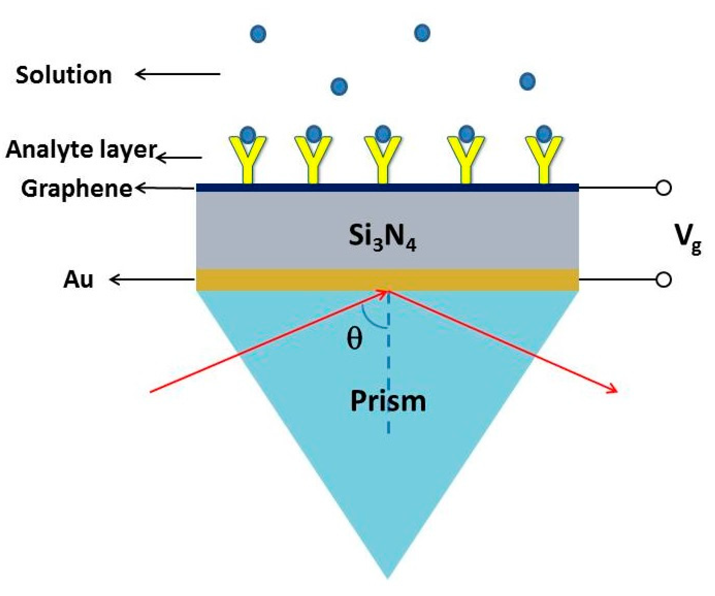
Figure 2.
(a) Relative permittivity of graphene as a function of its chemical potential under the conditions of λ=1310 nm, T=298 K, Γ=1e12 Hz; (b) the absolute value of relative permittivity with both wavelength and chemical potential in unit of hω/2π; (c) the absolute value of relative permittivity with both wavelength and chemical potential in unit of eV.
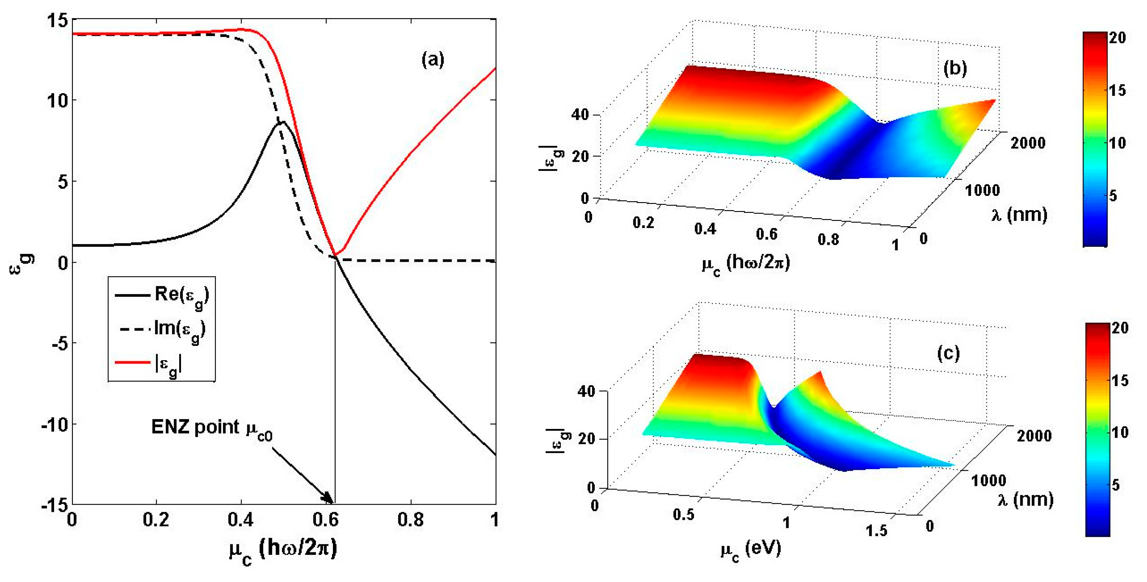
Figure 3.
Reflectance versus incident angle SPR curves for different prism materials when using monochromatic incident light beam with wavelength of: (a) 1100 nm; (b) 1200 nm; (c) 1310 nm; (d) 1550 nm; (e) 1700 nm; (f) 1900 nm.
Figure 3.
Reflectance versus incident angle SPR curves for different prism materials when using monochromatic incident light beam with wavelength of: (a) 1100 nm; (b) 1200 nm; (c) 1310 nm; (d) 1550 nm; (e) 1700 nm; (f) 1900 nm.
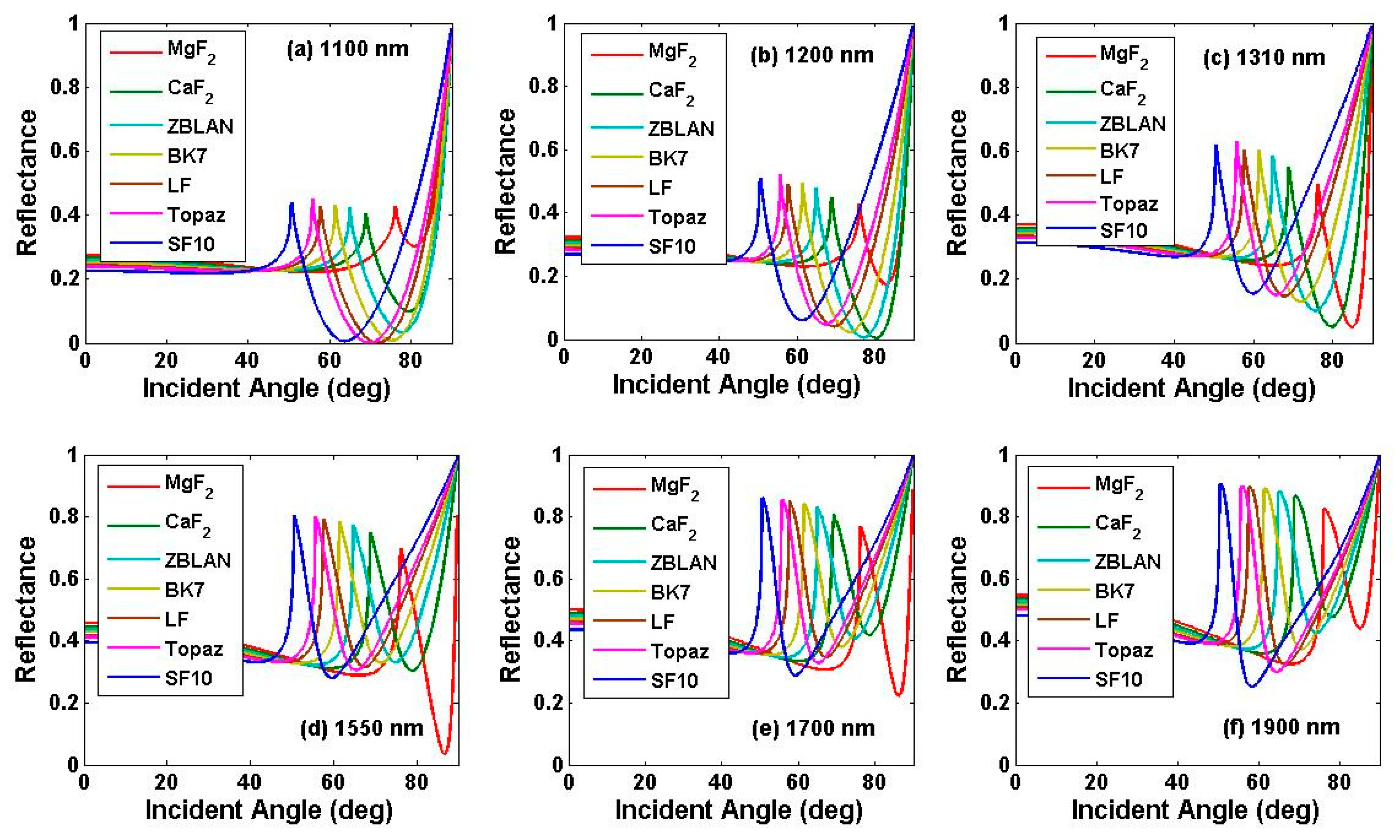
Figure 4.
Reflectance versus incident angle SPR curves for different thickness of the Au layer when using monochromatic incident light beam with wavelength of 1550 nm.
Figure 4.
Reflectance versus incident angle SPR curves for different thickness of the Au layer when using monochromatic incident light beam with wavelength of 1550 nm.
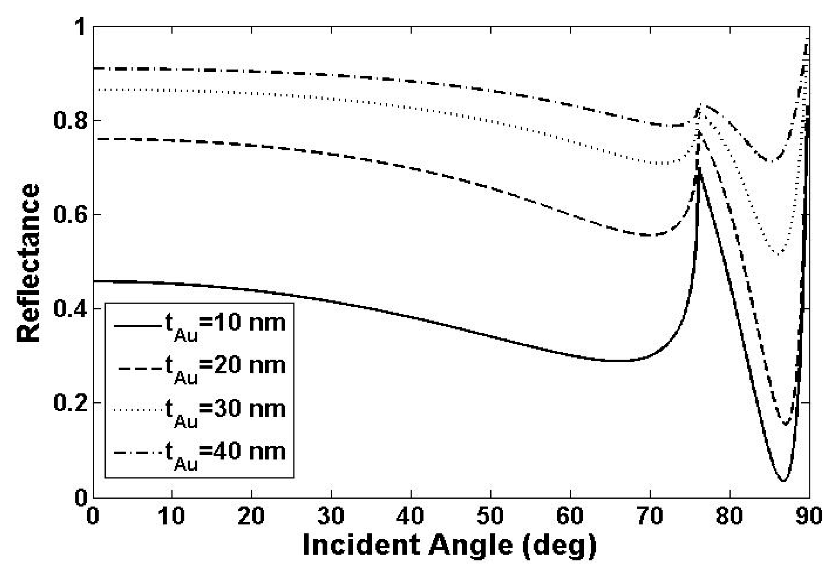
Figure 5.
Reflectance versus wavelength SPR curves for the chemical potential of graphene reach the PR point corresponding to different wavelengths: (a) μc=μcPR(1100nm); (b) μc=μcPR(1200nm); (c) μc=μcPR(1310nm); (d) μc=μcPR(1550nm); (e) μc=μcPR(1700nm); (f) μc=μcPR(1900nm).
Figure 5.
Reflectance versus wavelength SPR curves for the chemical potential of graphene reach the PR point corresponding to different wavelengths: (a) μc=μcPR(1100nm); (b) μc=μcPR(1200nm); (c) μc=μcPR(1310nm); (d) μc=μcPR(1550nm); (e) μc=μcPR(1700nm); (f) μc=μcPR(1900nm).
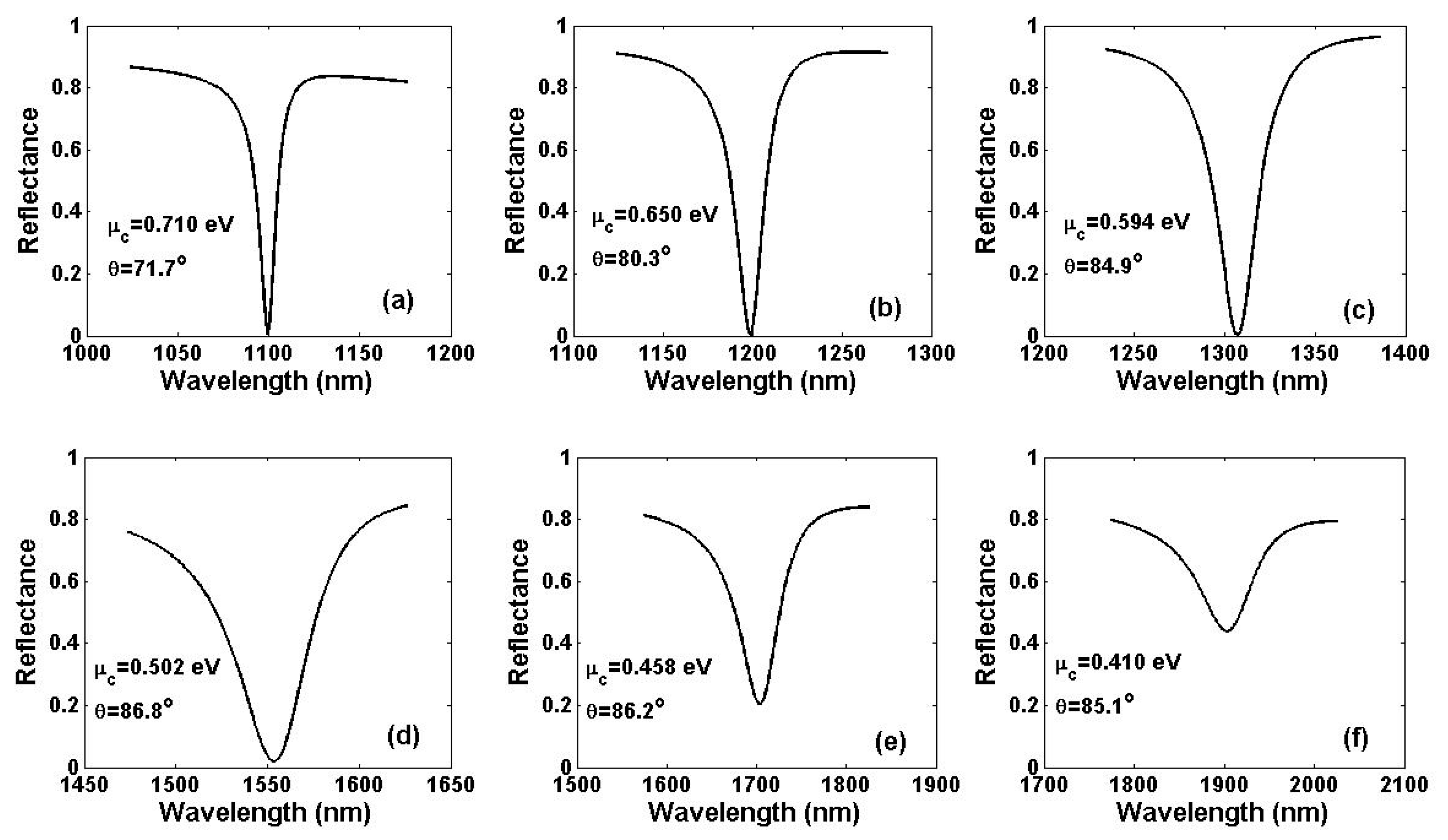
Figure 6.
The evolution of SPR curves at central wavelength of (a) 1100 nm; (b) 1200 nm; (c) 1310 nm; (d) 1550 nm; (e) 1700 nm; (f) 1900 nm respectively with the change of the refractive index of the analyte layer.
Figure 6.
The evolution of SPR curves at central wavelength of (a) 1100 nm; (b) 1200 nm; (c) 1310 nm; (d) 1550 nm; (e) 1700 nm; (f) 1900 nm respectively with the change of the refractive index of the analyte layer.

Figure 7.
The evolution of SPR curves at the central wavelength of (a) 1100; (b) 1200; (c) 1310; (d) 1550; (e) 1700; (f) 1900 nm respectively with the change of the chemical potential in graphene.
Figure 7.
The evolution of SPR curves at the central wavelength of (a) 1100; (b) 1200; (c) 1310; (d) 1550; (e) 1700; (f) 1900 nm respectively with the change of the chemical potential in graphene.
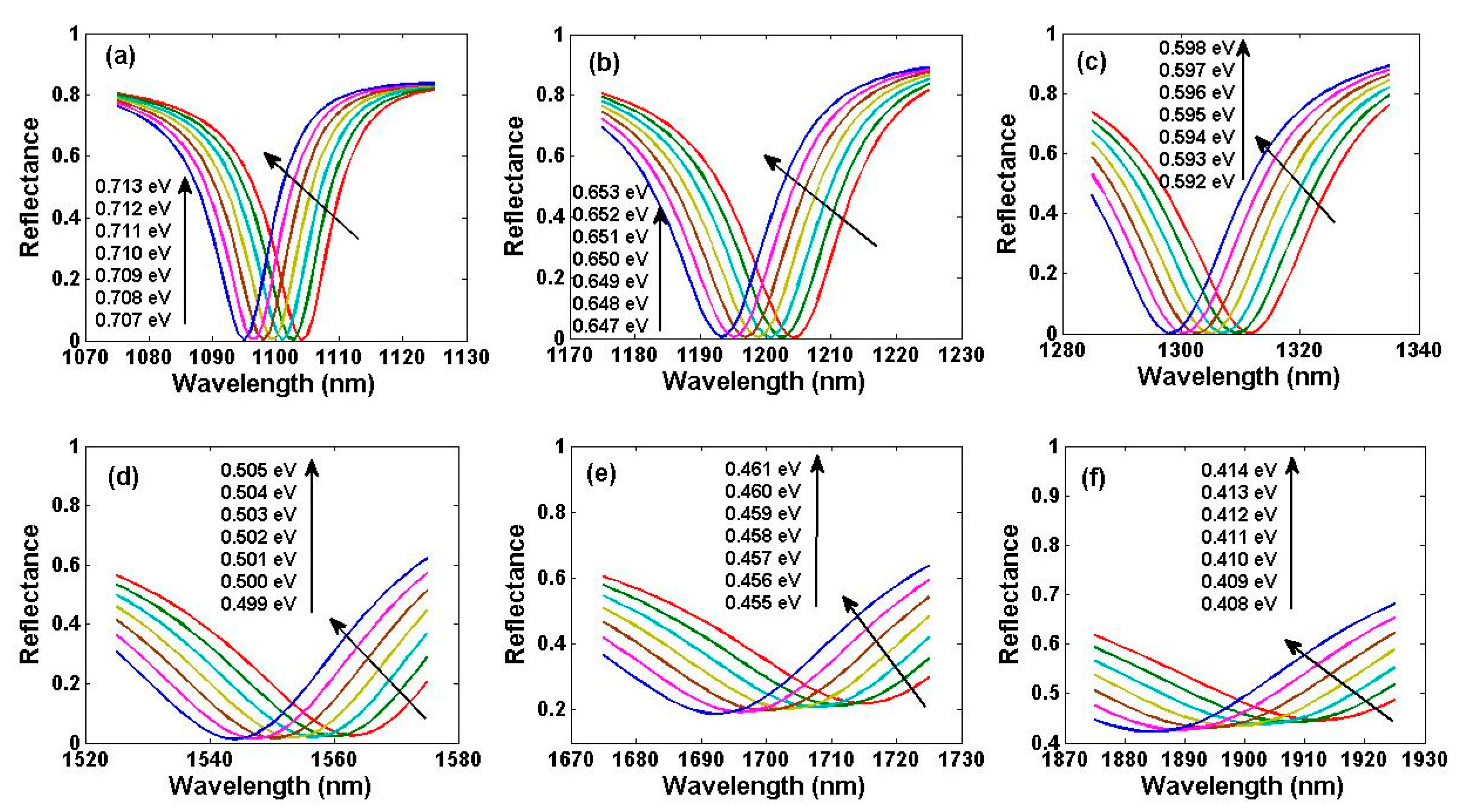
Figure 8.
(a) CP sensitivities (SCP) of resonance wavelength to the change of the chemical potential in graphene at different wavelengths; (b) RI sensitivities (S’RI) of resonance wavelength to the change of the refractive index in graphene at different wavelengths.
Figure 8.
(a) CP sensitivities (SCP) of resonance wavelength to the change of the chemical potential in graphene at different wavelengths; (b) RI sensitivities (S’RI) of resonance wavelength to the change of the refractive index in graphene at different wavelengths.
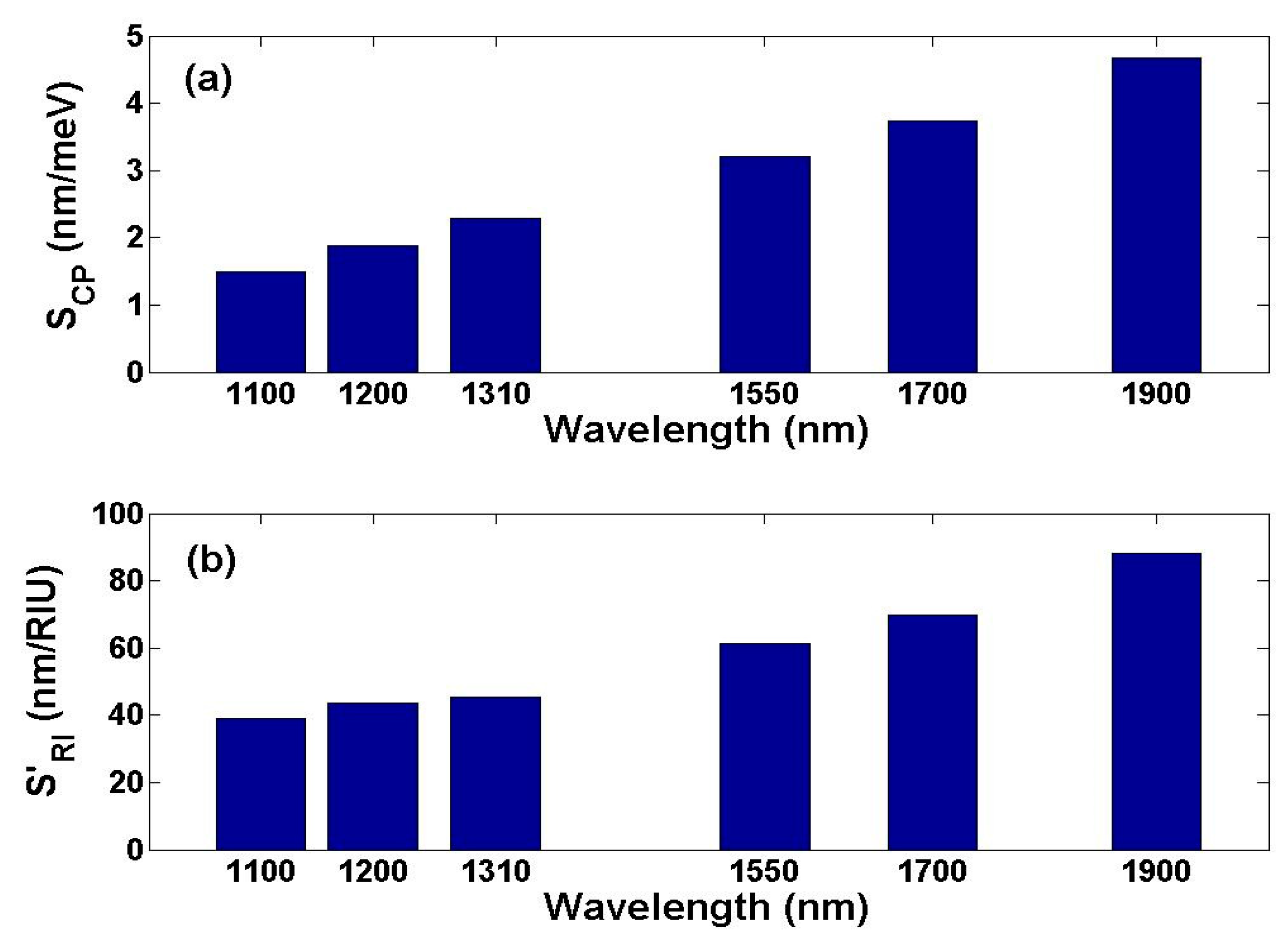
Figure 9.
(a) SPR curve in the waveband with 1310 nm as a central wavelength under the condition of θ=84.9°, MgF2 as prism material, μc=0.594 eV, the distributions of the electric field in the cross section of the multilayer system corresponding to resonance and un-resonance wavelength are displayed in the left and right inset respectively. The electric field intensity along the direction perpendicular to the prism interface for resonance wavelength (b) and un-resonance wavelength (c).
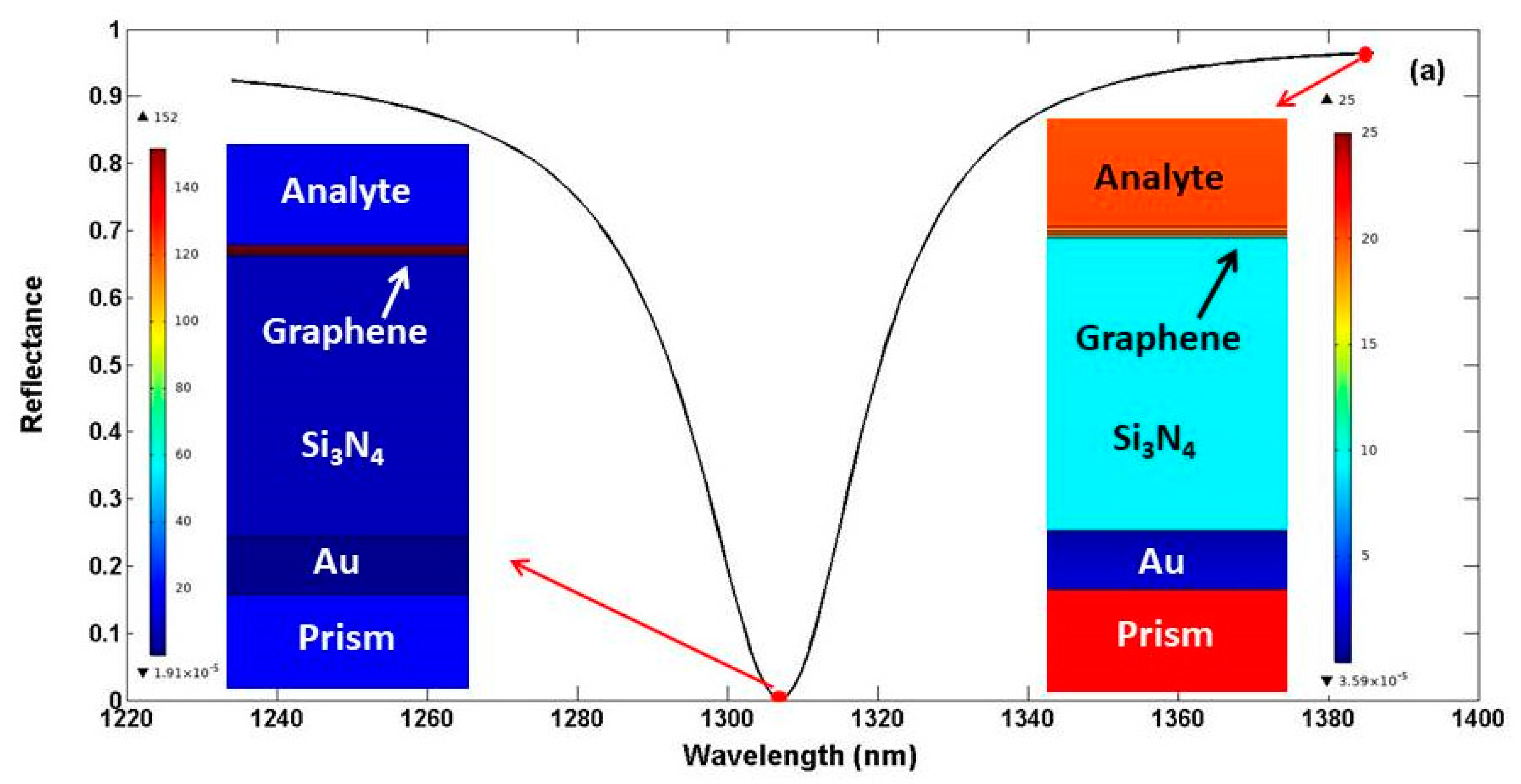
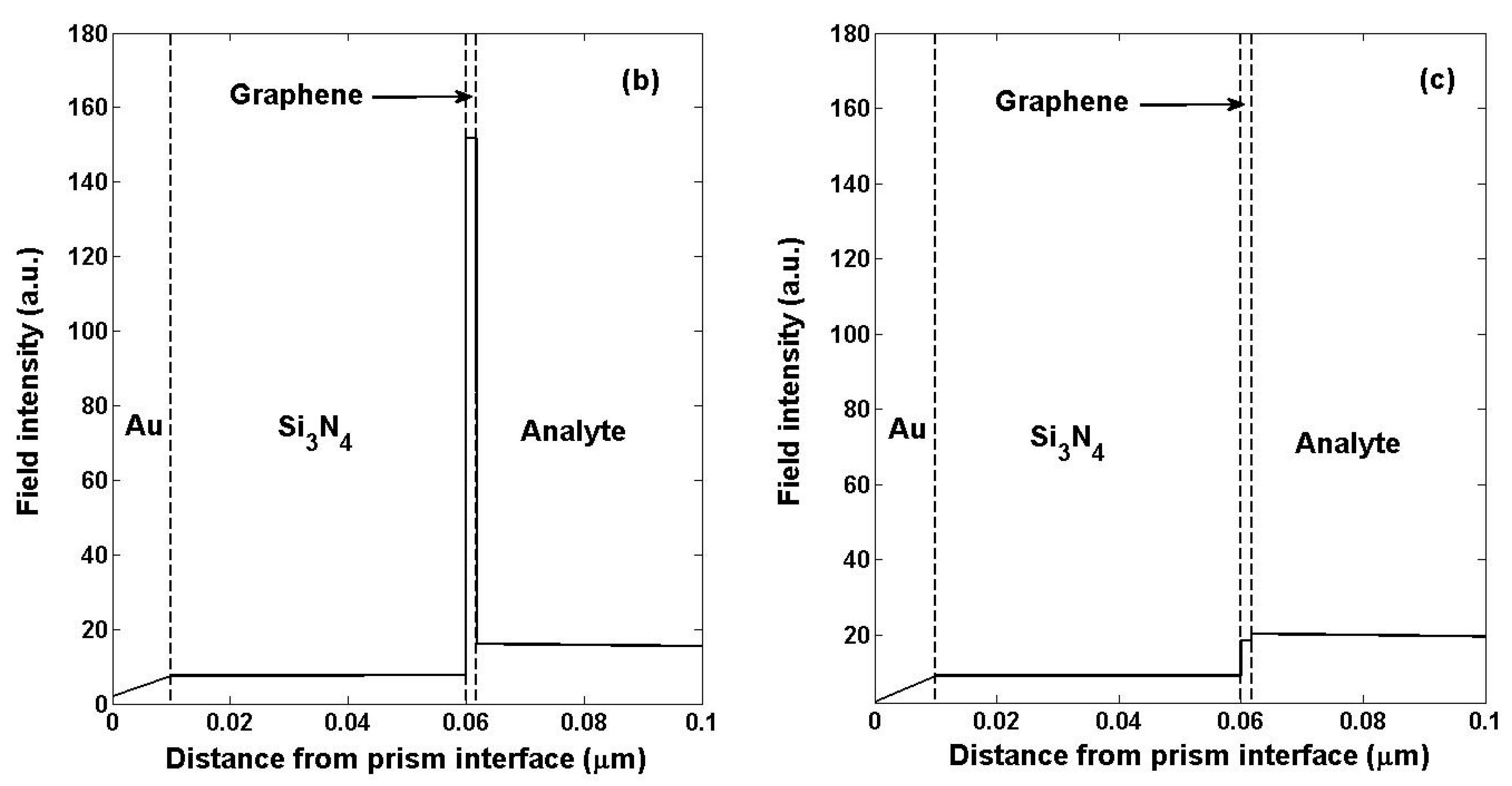
Figure 10.
The evolution of reflectance versus gate voltage SPR curves at the incident wavelength of: (a) 1100; (b) 1200; (c) 1310; (d) 1550; (e) 1700; (f) 1900 nm with the change of the initial chemical potential of the graphene film.
Figure 10.
The evolution of reflectance versus gate voltage SPR curves at the incident wavelength of: (a) 1100; (b) 1200; (c) 1310; (d) 1550; (e) 1700; (f) 1900 nm with the change of the initial chemical potential of the graphene film.
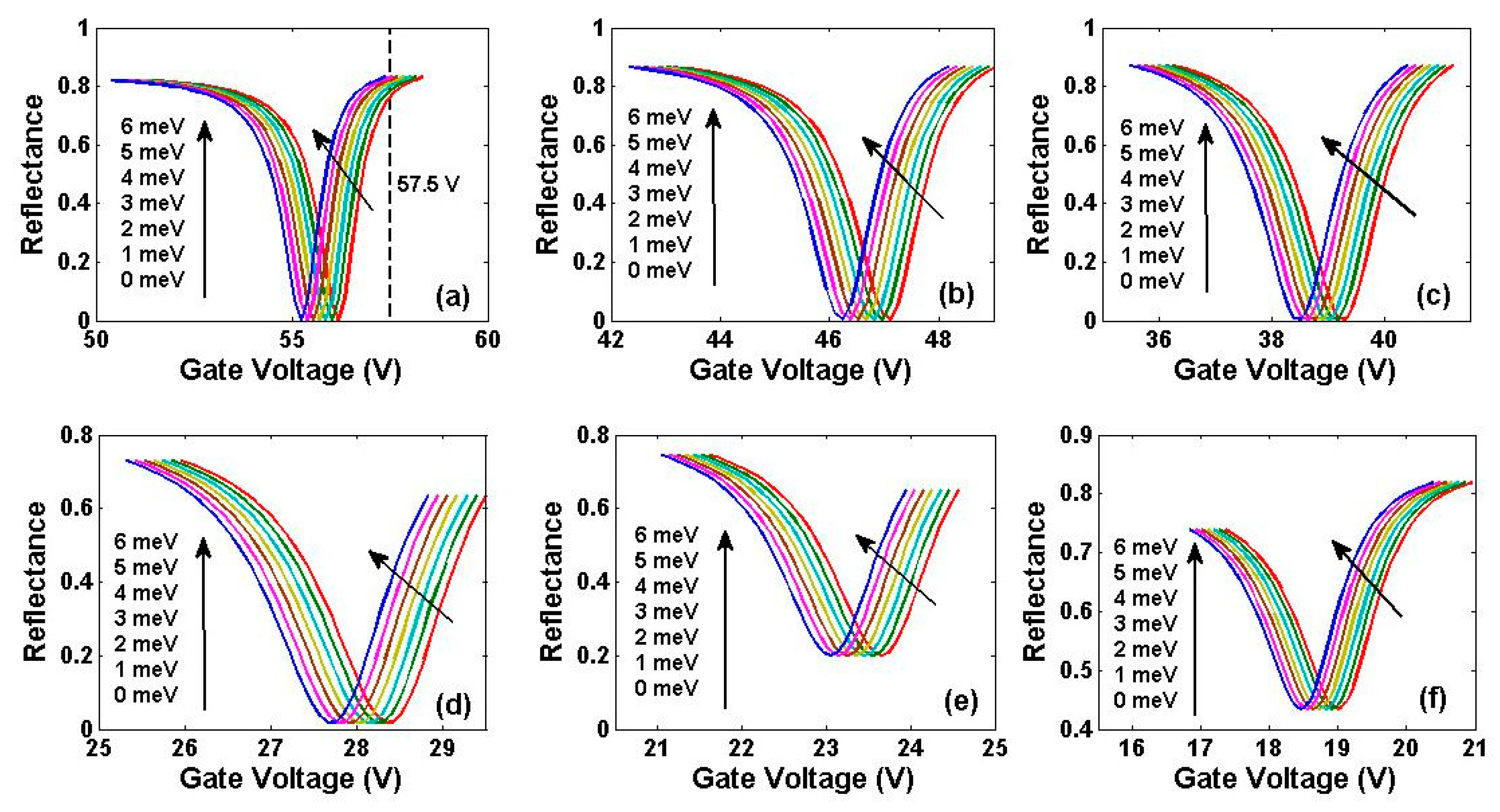
Figure 11.
CP sensitivities (S’cp) of the sensor in gate voltage interrogation mode at different incident light wavelengths.
Figure 11.
CP sensitivities (S’cp) of the sensor in gate voltage interrogation mode at different incident light wavelengths.
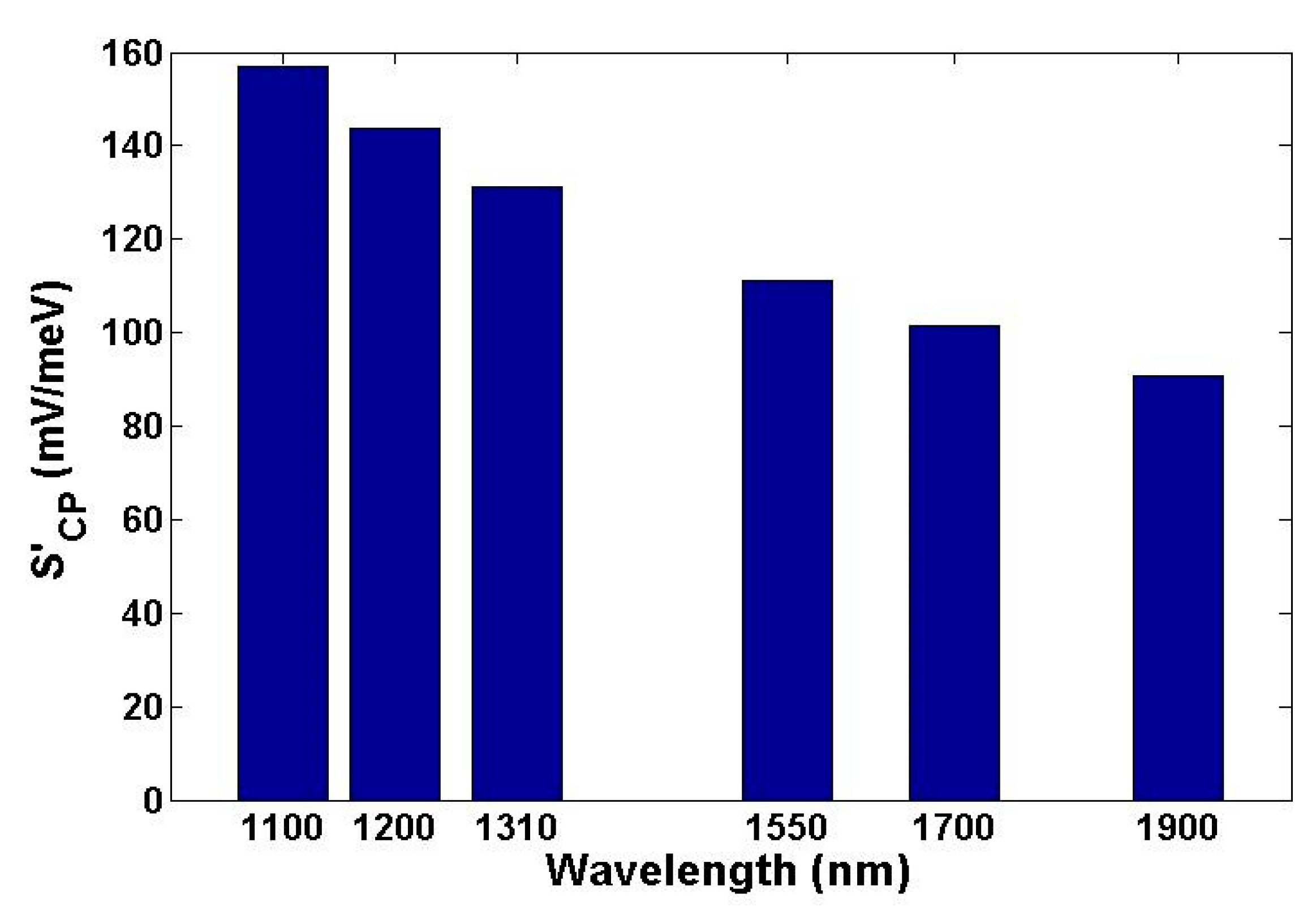
Figure 12.
(a) Reflectance versus wavelength SPR curves in the waveband with 1310 nm as a central wavelength for different scattering rate and N=5; (b) reflectance versus wavelength SPR curves in the waveband with 1310 nm as a central wavelength for different atom layer number and Γ=1e12; (c) reflectance versus gate voltage SPR curves of incident wavelength of 1310 nm for different scattering rate and N=5; (d) reflectance versus gate voltage SPR curves of incident wavelength of 1310 nm for different atom layer number and Γ=1e12.
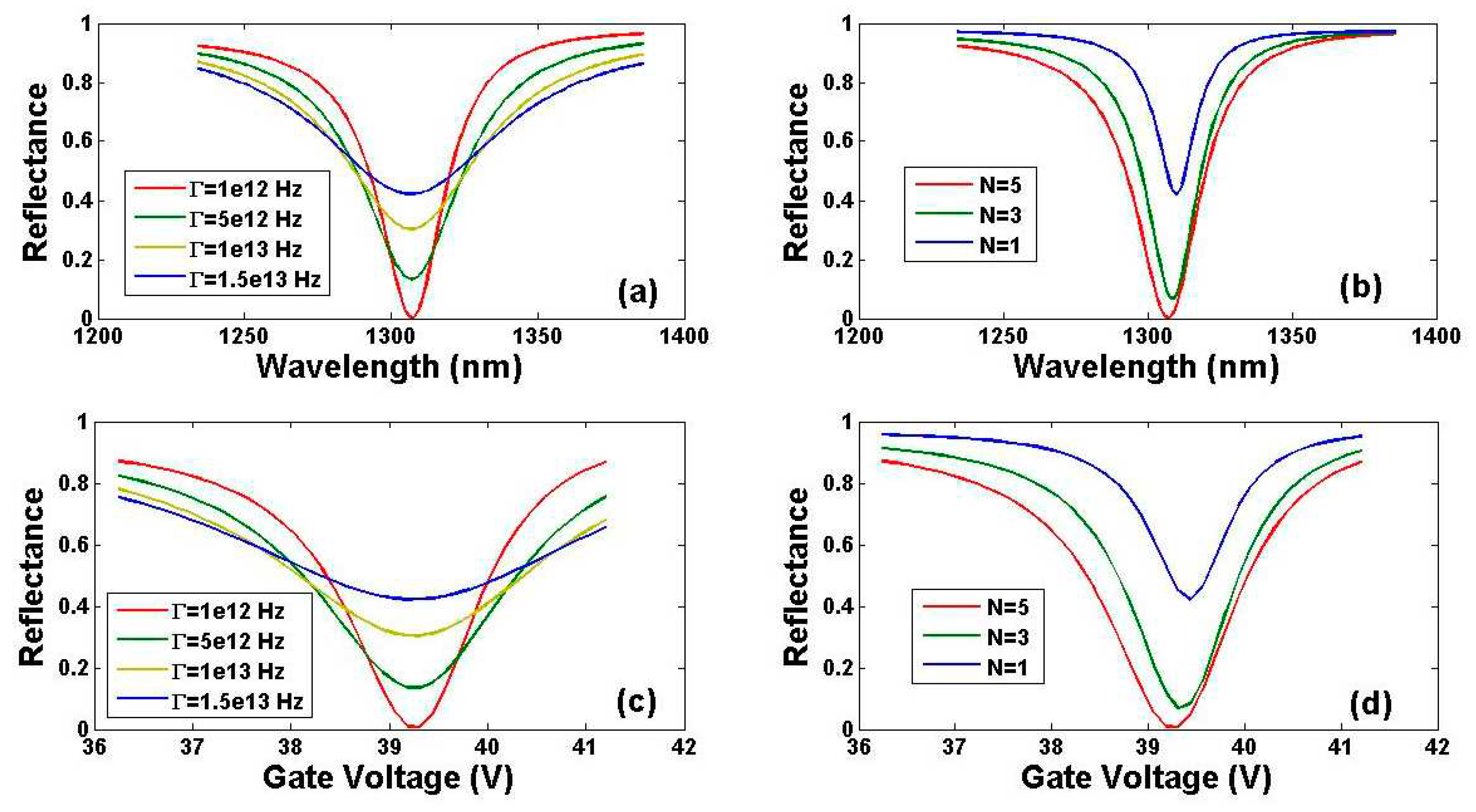
Table 1.
ENZ points, PR points, required gate voltages for trigging SPR effect of graphene at different wavelengths.
Table 1.
ENZ points, PR points, required gate voltages for trigging SPR effect of graphene at different wavelengths.
| λ(nm) | 760 | 850 | 980 | 1100 | 1200 | 1310 | 1550 | 1700 | 1900 |
|---|---|---|---|---|---|---|---|---|---|
| μc0(eV) | 1.037 | 0.923 | 0.798 | 0.709 | 0.649 | 0.594 | 0.502 | 0.458 | 0.410 |
| μcPR(eV) | 1.037 | 0.923 | 0.798 | 0.710 | 0.650 | 0.594 | 0.502 | 0.458 | 0.410 |
| Vg(V) | 119.6 | 94.8 | 70.9 | 56.2 | 47.1 | 39.4 | 28.2 | 23.5 | 18.9 |
Table 2.
The selected recent literatures on DNA detection by SPR manner since 2014.
| SPR structure | Theoretical/experimental | LOD | FWHM | Ref. |
|---|---|---|---|---|
| HBAK1/Au film/graphene/AuNSs | experimental | 0.5 fM | - | 14 |
| K9/Au film/graphene/AuNPs | experimental | 0.5 fM | - | 15 |
| K9/Au film/antimonene/AuNRs | experimental | 10 aM | - | 16 |
| K9/AuNT array/AuNPs | experimental | 1.2 aM | 114.471 nm | 17 |
| K9/Au film/GO-AuNPs | experimental | 0.2 fM | - | 18 |
| MgF2/Au film/Si3N4/graphene | theoretical | <4.27 fM | 78.4 nm | this work |
| LF/Au film/Si3N4/graphene | theoretical | <21.66 aM | 1158 mV | this work |
Disclaimer/Publisher’s Note: The statements, opinions and data contained in all publications are solely those of the individual author(s) and contributor(s) and not of MDPI and/or the editor(s). MDPI and/or the editor(s) disclaim responsibility for any injury to people or property resulting from any ideas, methods, instructions or products referred to in the content. |
© 2023 by the authors. Licensee MDPI, Basel, Switzerland. This article is an open access article distributed under the terms and conditions of the Creative Commons Attribution (CC BY) license (http://creativecommons.org/licenses/by/4.0/).
Copyright: This open access article is published under a Creative Commons CC BY 4.0 license, which permit the free download, distribution, and reuse, provided that the author and preprint are cited in any reuse.


