
Submitted:
24 October 2023
Posted:
24 October 2023
You are already at the latest version
Abstract
An ultraviolet (UV) nanosecond pulsed laser with a wavelength of 355 nm was applied to anneal amorphous indium-gallium-zinc oxide (a-IGZO) thin-film transistors (TFT) at various laser beam powers ranging from 0 to 280 mW. Laser irradiation was selectively carried out on the a-IGZO channel area using the beam scanning method after the a-IGZO TFT was formed through indium-tin oxide (ITO) electrode patterning and a subsequent lift-off process. After laser annealing, negative shifts in the threshold voltages and enhanced on-currents were observed at laser-beam powers ranging from 54 to 120 mW. No meaningful parameters were investigated for laser beams higher than 200 mW. By extracting the energy band gap and work function of a-IGZO from the transmittance and ultraviolet photoelectron spectroscopy (UPS) results, the ITO electrode/a-IGZO channel energy band structures were established under different laser annealing conditions, and the electron injection mechanism from the ITO to the a-IGZO channel was analyzed and optimized at a laser beam power of 120 mW. The results show that the electrical characteristics of the a-IGZO TFTs can be improved without any heat damage to the substrate because of the selective annealing process.
Keywords:
UV pulsed laser annealing
; a-IGZO TFT
; ITO/IGZO energy band structure
; selective annealing
1. Introduction
Metal-oxide semiconductors are of interest as core materials for next-generation displays owing to their advantages of low off-current and low-temperature processing. In particular, metal-oxide semiconductors are deposited by low-temperature sputtering, and process compatibility can result in better uniformity over a large area and higher reliability over a longer time [1,2,3,4,5,6]. Amorphous indium-gallium-zinc oxide (a-IGZO) has been widely used as a channel material for thin-film transistors (TFT) because of its moderate electron affinity, low threshold voltage, and high transmittance caused by its high-energy band gap [7,8,9,10,11,12]. Although a-IGZO has a relatively high energy bandgap, the orbital overlap of indium and oxygen vacancies in the zinc oxide (ZnO) structure enables high electron mobility and electrical conduction [13,14,15]. The ionic bonding of IGZO makes maintaining high carrier mobility possible in amorphous metal-oxide semiconductors, in contrast to the covalent bonding of amorphous Si. At a positive gate voltage (on position), an a-IGZO TFT can show 20–50 times higher electrical current than a hydrogenated amorphous silicon (a-Si:H) TFT, and the off-leakage current of an a-IGZO TFT is much lower than that of low-temperature polysilicon (LTPS) TFT [16]. Therefore, a higher speed without motion blur or low power consumption can be obtained while driving the display.
In previous studies, in the fabrication process of a-IGZO TFT, to improve the electrical stability and reliability of a-IGZO thin films, they were thermally annealed using an oven, a vacuum furnace, and rapid thermal annealing (RTA). Considering the melting point of the soda-lime glass substrate, the annealing temperatures have been mainly maintained under 500–600 °C [17,18,19,20]. However, the completion of the annealing process takes a relatively long time because of the cooling process time in RTA and the stabilization time in a vacuum furnace. Moreover, the conventional annealing temperature is so high that it is not suitable for flexible substrates such as polyimide (PI) or polyethylene terephthalate (PET). As a new low-temperature rapid annealing process, we applied a xenon (Xe) flash lamp for the annealing of a-IGZO TFT, which showed enhanced electrical characteristics [21]. However, Xe flash lamps are also applied to the entire area of the substrate, and unexpected side effects such as electrode damage can occur [22].
For the selective annealing process, a laser beam was used in the fabrication of a-Si:H TFT, and an LTPS TFT was realized and used as the driving TFT in active matrix organic light-emitting diode (AMOLED) displays. This process, however, has some drawbacks, such as the high cost of laser equipment and damage to thin films caused by laser beam tracing [23,24]. Because the laser beam energy is not transferred thermally, no cooling is required during the annealing process, and the process can be completed in a short time. Furthermore, laser beams can be easily optimized by controlling parameters such as their pulse duration, frequency, and scanning speed [25,26,27].
In this study, we irradiated an a-IGZO TFT with a 355 nm ultraviolet (UV)-pulsed laser and investigated and analyzed the annealing effect on the electrical characteristics of the TFT. Considering the TFT size used in the display industry, a-IGZO TFTs with channel lengths of less than 10 mm were fabricated using source/drain photolithography and liftoff processes for IGZO channel formation. Indium tin oxide (ITO) was used as a source/drain electrode to avoid laser-induced damage to the metal electrodes. Upon fabrication of the a-IGZO TFT, the 355 nm UV pulsed laser beam was selectively irradiated on the a-IGZO channel layer using the scanning method. The laser beam energy was controlled from 54 mW to 280 mW by adjusting the off time. The electrical characteristics and the effect of the laser beam energy were analyzed. To investigate the structural characteristics of the laser-annealed a-IGZO TFT, a-IGZO thin films were deposited on glass and Si wafer substrates, and the laser beam was irradiated under identical conditions.
2. Experimental Methods
Figure S1 shows the sequence of the fabrication process of the a-IGZO/ITO TFT. A boron-doped p-type silicon wafer with a resistivity of 1–10 Ω ▪cm was used as a substrate. For the gate dielectric layer of the TFT, silicon dioxide (SiO2) was thermally grown on a Si wafer. Before the ITO sputtering process, the silicon wafer was cleaned with isopropyl alcohol (IPA), acetone, and deionized (DI) water in an ultrasonic bath for 15 min. After the cleaned silicon wafer was vertically loaded into a jig in the load-lock chamber, it was moved to the process chamber of the in-line sputter. The silicon substrate was moved in front of a 99.99% indium tin oxide (ITO) target of size 165 mm × 540 mm × 7 mm (InO3:SnO2 = 90:10) at a base vacuum of 9×10⁻⁶ Torr, and plasma was generated with a DC power of 2 kW at a pressure of 4 mTorr and at room temperature. Ar and O2 gas injections were maintained at 50 and 1.2 sccm, respectively [28,29]. During the ITO sputtering, the jig was scanned in front of the ITO target at a speed of 45 cm/min (15 Hz). The thickness and sheet resistance of the ITO target were about 80 nm and 65.5±0.6 ohm/sq, respectively.
For photolithography of the ITO electrode, an AZ GXR 601 positive photoresist (PR) was used for spin-coating at a speed of 4000 rpm. After the PR was soft-baked on a hot plate at 90 °C for 60 s, it was irradiated with UV light for 3 sec through a source and drain Cr pattern on the photo mask. The distance between the mask and photo mask was maintained at 100 mm. PR source and drain development was carried out using AZ 300 MIF developer solution after post-exposure baking on a hot plate at 110 °C for 60 s. The PR was hard-baked, and the ITO source and drain patterns were obtained by wet etching using an AP-KIT ITO etchant at room temperature for 20–30 s, as shown in Figure S1(a). The widths of the mask patterns were designed to be 20, 40, and 60 mm, and the lengths were 2, 3, 4, 5, and 6 mm. For patterning the IGZO active layer, PR patterns were developed using the same photolithography process parameters as for ITO patterning, as shown in Figure S1(b). Figure S1(c) shows the a-IGZO active layer deposited with a thickness of 30 nm using radio frequency (RF) sputtering at room temperature for 3 min 30 s. An IGZO target with a diameter of 4 in and thickness of 1/8 in (In2O3:Ga2O3:ZnO = 1:1:1) was used, and plasma was generated with an RF power of 60 W at a pressure of 4 mTorr. The lift-off process was performed using acetone dipping and N2 blowing, and an IGZO/ITO TFT was obtained, as shown in Figure S1(d).
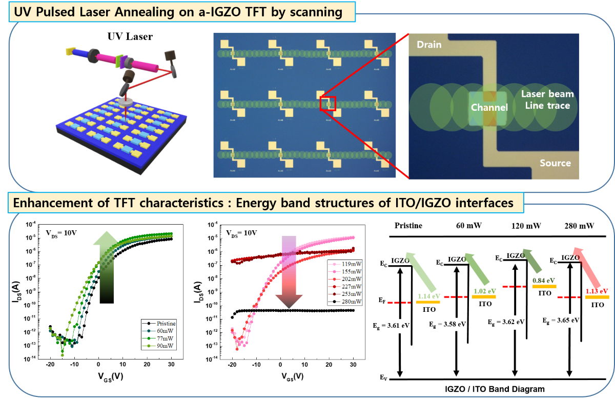
Figure 1(a) shows the 355 nm UV pulsed laser system used for the laser annealing of the a-IGZO/ITO TFT. The laser power was controlled precisely by rotating the half-wave plate installed in front of the polarized beam splitter. The laser beam was scanned across the a-IGZO channel layers of a-IGZO/ITO TFTs using a galvanometer. The diameter and repetition rate of the laser beam were fixed at 20 mm and 100 kHz, respectively. The laser-beam scanning speed was maintained at 100 mm/s, and the scanning direction was aligned for application to multiple TFTs in a single stroke, as shown in Figure 1(b). Laser annealing was performed at laser powers ranging from 0 (no annealing) to 280 mW.
The current-voltage characteristics of the laser-annealed a-IGZO/ITO TFT were measured using a probe station and parameter analyzer (HP-4156 C). The laser scanning traces were investigated using a high-resolution scanning electron microscope (Hitachi S-4700). The transmittance and absorbance of the laser-annealed a-IGZO were measured using a UV visible spectrometer (VARIAN, Cary 100). To analyze the energy band structure of the laser-annealed a-IGZO, the cutoff energy and valence band maxima (VBM) were obtained using ultraviolet photoelectron spectroscopy (UPS) (Thermo Fisher Scientific, ESCALAB 250).
3. Results and Discussion
3.1. Current-Voltage Characteristics Depending on the UV Pulsed Laser Beam Energy
Because the electrical characteristics were obtained from a-IGZO TFTs with different channel widths and lengths, the transfer and output characteristics of the a-IGZO TFTs after laser annealing (Figure 2) were normalized for comparison. Figure 2(a) shows the transfer characteristics of the a-IGZO TFTs after laser annealing at laser beam energies ranging from pristine (no annealing) to 90 mW. As the laser beam energy increased to 90 mW, the threshold voltage (VTH) shifted in the negative direction, and the on/off current ratio increased. The subthreshold swing (S.S.) was also slightly reduced from 2.0 V/dec to 1.66 V/dec, as shown in Table 1. However, for higher laser beam energies ranging from 119 to 280 mW, the electrical parameters were steeply degraded, as shown in Figure 1(b). Furthermore, above 200 mW, no transfer characteristics were investigated, and no device parameters were obtained, as shown in Table 1. Figure 1(C), (D), and (E) show the output characteristics of the a-IGZO TFTs for laser beam energies of 0 (pristine), 55, and 90 mW, respectively. When the gate-to-source voltage (VGS) was increased from 5 to 25 V, the drain-to-source current distinctly increased when the laser beam power was 55 mW and 77 mW. The enhanced on-current is thought to result from laser annealing.
Table 1 shows the dependence of the device parameters such as VTH, S.S., saturation mobility, and on/off current ratio (Ion/Ioff) on the laser beam energy. As shown in Figure 1(b), when the laser beam was higher than 200 mW, an off-current was generated and was constant regardless of the value of VGS. Similar results were obtained for the 308 nm XeCl excimer laser annealing, 248 nm KrF excimer laser annealing, and 800 nm femtosecond laser annealing of sputtered IGZO TFTs [26,30,31]. The unstable electrical characteristics are expected to be due to the damage to devices caused by excessive laser beam energy and excessive carriers resulting from laser annealing. In particular, degradation by laser annealing is more effective for small-dimensional TFTs based on a two-dimensional heat simulation of laser heating [31]. As the laser beam energy was increased to 90 mW, the enhanced on-current may have affected Ion/Ioff, and the S.S. was also slightly improved. However, no dependency or relationship between mobility and laser beam energy was investigated. In the case of CO2 laser spiking annealing (LSA) of a-IGZO TFT, the optimized LSA condition that enhances the saturation mobility of the laser-annealed TFT is difficult to find because improvements in mobility are not dependent on the LSA condition determined by peak temperatures and dwell time [32]. Figure 3 shows that VTH linearly negatively shifted as the laser beam energy increased, and its mechanism may be explained by the limitation of the relaxation of structural defects. In contrast to conventional thermal annealing, the time required to prevent oxygen vacancies from being ionized and to compensate for laser-induced damage may be impossible to achieve because of the limited timescale [32,33].
3.2. Structural Characteristics and Energy Band Analysis with Laser Beam Energy
During the laser scanning of the a-IGZO TFT, the beam diameter (20 mm) was much larger than the TFT channel length (2–6 mm). In addition, the direction of laser scanning was manually aligned parallel to the multiple TFT channels, as shown in Figure 1(b). To analyze the structural characteristics of the laser-annealed TFT, Figure 4(A), (B), and (C) show the scanning electron microscopy (SEM) images of the a-IGZO TFT, laser-annealed at powers of 0 (pristine), 77 mW, and 227 mW, respectively. As shown in Figure 4(B), no laser beam traces or etching residues were observed at the laser beam energy of 77 mW. No apparent dependence of the a-IGZO layers on the laser beam energy was observed. The laser line scanning traces were observed at 227 mW, as shown in the left image of Figure 4(C). All the laser-annealed TFTs were observed using SEM, and laser line traces were found for laser beam energies higher than 200 mW (Figure S2). The line beam traces may result in laser-induced damage to the a-IGZO TFTs and degraded electrical characteristics, such as a high off-current.
To further analyze the enhanced on-current and negatively shifted VTH of the laser-annealed a-IGZO TFTs, the optical bandgaps of the laser-annealed a-IGZO layers were obtained by measuring the transmittance data. a-IGZO thin films were RF-sputtered on soda-lime glass substrates under the same process conditions as for TFT fabrication, and a 355 nm UV pulsed laser was irradiated at energies of 0 (pristine), 60 mW, 120 mW, and 280 mW.
Figure 5(A) and (B) show the transmittance data of the laser-annealed a-IGZO thin films and the absorbance calculated using the logarithm of the reciprocal of 5(A), respectively. For wavelengths above 400 nm, all a-IGZO thin films showed transmittances higher than 80%, and the average transmittances from 380 to 780 nm were 87.54%, 87.18%, 88.45%, and 89.22% for laser energies of 0 (pristine), 60, 120, and 280 mW, respectively. The transmittance increased slightly as the laser beam energy increased. From the absorbance data in Figure 5(B) and the thicknesses of the a-IGZO thin films, the optical bandgap of the laser-annealed a-IGZO layer was calculated using a Tauc plot, as shown in Figure 6. The optical bandgap of a-IGZO was 3.61 eV, 3.58 eV, 3.62 eV, and 3.65 eV for laser powers of 0 (pristine), 60 mW, 120 mW, and 280 mW, respectively.
To obtain the energy band structures of the laser-annealed a-IGZO layers, UPS spectra were measured for the laser-annealed a-IGZO thin films on p-type silicon wafers, as shown in Figure 7(A). The RF sputtering and laser-annealing conditions were the same as those shown in Figure 5 and Figure 6. The cutoff energy and VBMs were extracted from enlarged Figure 7(B) and 7(C), respectively [34].
Figure 8(A) shows the energy band diagrams of the laser-annealed a-IGZO thin films designed using the work functions calculated from Figure 7(B) and the VBMs extracted from Figure 7(C). From the vacuum energy level, the work functions were calculated as 4.11 eV, 4.16 eV, 4.13 eV, and 4.22 eV for laser energies of 0 (pristine), 60 mW, 120 mW, and 280 mW, respectively. The VBMs were extracted as 6.58 eV, 6.72 eV, 6.91 eV, and 6.78 eV from the vacuum energy level for laser energies of 0 (pristine), 60 mW, 120 mW, and 280 mW, respectively. Considering the optical energy bandgaps in Figure 6, the conduction band minimum (CBM) was calculated as 2.97 eV, 3.14 eV, 3.29 eV, and 3.08 eV from the vacuum energy level for laser energies of 0 (pristine), 60, 120, and 280 mW, respectively.
The junction between the ITO electrode and a-IGZO channel layers was described for different laser beam energies, as shown in Figure 8(B). Considering that the Fermi energy of ITO is identical to that of a-IGZO, the difference between CBM and Fermi energy of a-IGZO and the energy barrier for electrons to move from ITO to the conduction band of a-IGZO was calculated as 1.14 eV, 1.02 eV, 0.84 eV, and 1.13 eV for laser energies of 0 (pristine), 60 mW, 120 mW, and 280 mW, respectively. The optimized laser beam energy was 120 mW, which is the distance between the Fermi level and the conduction band of a-IGZO. Therefore, the energy barrier between the ITO electrode and the channel was reduced, leading to an enhancement in the carrier concentration and on-current.
4. Conclusions
We investigated the effect of 355 nm ultraviolet nanosecond pulsed laser annealing on the performance of amorphous indium-gallium-zinc oxide thin-film transistors. Devices selectively laser-irradiated using a beam scanning method in the a-IGZO channel region showed a negative shift in threshold voltage and on-current enhancement at laser beam powers ranging from 54 to 120 mW. To investigate the mechanism of laser annealing, we performed UPS analysis and found that the energy barrier between the CBM and Fermi level decreased, resulting in an increase in the carrier concentration at the surface. SEM analysis confirmed that no heating damage occurred on the substrate at laser beam powers lower than 120 mW during the process. Therefore, the ultraviolet nanosecond pulsed laser annealing process improves the electrical characteristics of the a-IGZO TFT and can be applied to flexible substrates with temperature limitations.
Supplementary Materials
The following supporting information can be downloaded at the website of this paper posted on Preprints.org, Figure S1: Fabrication process of an a-IGZO/ITO TFT (a) ITO sputtering and patterning (b) photolithography for lift-off (c) IGZO sputtering (d) lift-off; Figure S2: SEM images of a-IGZO TFTs after a 355 nm UV pulsed laser annealing process for laser beam energies of (a) 119 mW, (b) 155 mW, (c) 202 mW, (d) 227 mW, (e) 250 mW, and (c) 280 mW.
Author Contributions
S. Y. P. and Y. C.: Fabrication and electrical and structural characterization of the a-IGZO TFT; Y. H. S.: Structural characterization of a-IGZO thin films; H. K. and P. L. T.: Laser irradiation; D. H. L and H. Y.: UPS measurements and analyses; Y. J. and S. J. K.: Discussion and validation; D. L.: Conceptualization and laser irradiation; and E. –S. C: Conceptualization, writing-original draft preparation, project administration, resources, and supervision. All the authors have read and agreed to the published version of the manuscript.
Funding
This work was supported by a National Research Foundation of Korea (NRF) grant funded by the Korean government (MSIT) (No. NRF-2020R1F1A1076505) and partly supported by the Korea Institute for Advancement of Technology (KIAT) grant funded by the Korean government (MOTIE) (No. P0012453, The Competency Development Program for Industry Specialists). This study was supported by the Gachon University Research Fund 2021 (GCU−202110210001).
Data Availability Statement
The data supporting the findings of this study are available from the corresponding author upon request.
Conflicts of Interest
The authors declare no conflicts of interest.
References
- Naqi, M.; Cho, Y.; Kim, S. High-Speed Current Switching of Inverted-Staggered Bottom-Gate a-IGZO-Based Thin-Film Transistors with Highly Stable Logic Circuit Operations. ACS Applied Electronic Materials 2023, 5, 3378–3383. [Google Scholar] [CrossRef]
- Fortunato, E.; Barquinha, P.; Martins, R. Oxide Semiconductor Thin-Film Transistors: A Review of Recent Advances. Advanced Materials 2012, 24, 2945–2986. [Google Scholar] [CrossRef] [PubMed]
- Ji, X.; Yuan, Y.; Yin, X.; Yan, S.; Xin, Q.; Song, A. High-Performance Thin-Film Transistors With Sputtered IGZO/Ga₂O₃ Heterojunction. IEEE Transactions on Electron Devices 2022, 69, 6783–6788. [Google Scholar] [CrossRef]
- Striakhilev, D.; Park, B.-K.; Tang, S.-J. Metal oxide semiconductor thin-film transistor backplanes for displays and imaging. MRS Bulletin 2021, 46, 1063–1070. [Google Scholar] [CrossRef]
- Park, J.S.; Maeng, W.-J.; Kim, H.-S.; Park, J.-S. Review of recent developments in amorphous oxide semiconductor thin-film transistor devices. Thin Solid Films 2012, 520, 1679–1693. [Google Scholar] [CrossRef]
- Nomura, K. Recent progress of oxide-TFT-based inverter technology. Journal of Information Display 2021, 22, 211–229. [Google Scholar] [CrossRef]
- Hosono, H. Ionic amorphous oxide semiconductors: Material design, carrier transport, and device application. Journal of Non-Crystalline Solids 2006, 352, 851–858. [Google Scholar] [CrossRef]
- Kamiya, T.; Hosono, H. Material characteristics and applications of transparent amorphous oxide semiconductors. NPG Asia Materials 2010, 2, 15–22. [Google Scholar] [CrossRef]
- Wu, G.M.; Liu, C.Y.; Sahoo, A.K. RF sputtering deposited a-IGZO films for LCD alignment layer application. Applied Surface Science 2015, 354, 48–54. [Google Scholar] [CrossRef]
- Troughton, J.; Atkinson, D. Amorphous InGaZnO and metal oxide semiconductor devices: an overview and current status. Journal of Materials Chemistry C 2019, 7, 12388–12414. [Google Scholar] [CrossRef]
- Kamiya, T.; Nomura, K.; Hosono, H. Present status of amorphous In–Ga–Zn–O thin-film transistors. Science and Technology of Advanced Materials 2010, 11. [Google Scholar] [CrossRef] [PubMed]
- Kang, D.H.; Kang, I.; Ryu, S.H.; Jang, J. Self-Aligned Coplanar a-IGZO TFTs and Application to High-Speed Circuits. IEEE Electron Device Letters 2011, 32, 1385–1387. [Google Scholar] [CrossRef]
- De Jamblinne De Meux, A.; Bhoolokam, A.; Pourtois, G.; Genoe, J.; Heremans, P. Oxygen vacancies effects in a-IGZO: Formation mechanisms, hysteresis, and negative bias stress effects. physica status solidi (a) 2017, 214, 1600889. [Google Scholar] [CrossRef]
- Nomura, K.; Ohta, H.; Takagi, A.; Kamiya, T.; Hirano, M.; Hosono, H. Room-temperature fabrication of transparent flexible thin-film transistors using amorphous oxide semiconductors. Nature 2004, 432, 488–492. [Google Scholar] [CrossRef]
- Jianke, Y.; Ningsheng, X.; Shaozhi, D.; Jun, C.; Juncong, S.; Shieh, H.D.; Po-Tsun, L.; Yi-Pai, H. Electrical and Photosensitive Characteristics of a-IGZO TFTs Related to Oxygen Vacancy. IEEE Transactions on Electron Devices 2011, 58, 1121–1126. [Google Scholar] [CrossRef]
- Inoue, H.; Matsuzaki, T.; Nagatsuka, S.; Okazaki, Y.; Sasaki, T.; Noda, K.; Matsubayashi, D.; Ishizu, T.; Onuki, T.; Isobe, A.; Shionoiri, Y.; Kato, K.; Okuda, T.; Koyama, J.; Yamazaki, S. Nonvolatile Memory With Extremely Low-Leakage Indium-Gallium-Zinc-Oxide Thin Film Transistor. IEEE Solid-State Circuits 2012, 47, 2258. [Google Scholar] [CrossRef]
- Lee, H.-W.; Cho, W.-J. Effects of vacuum rapid thermal annealing on the electrical characteristics of amorphous indium gallium zinc oxide thin films. AIP Advances 2018, 8, 015007. [Google Scholar] [CrossRef]
- Peng, C.; Yang, S.; Pan, C.; Li, X.; Zhang, J. Effect of Two-Step Annealing on High Stability of a-IGZO Thin-Film Transistor. IEEE Transactions on Electron Devices 2020, 67, 4262–4268. [Google Scholar] [CrossRef]
- Lee, M.K.; Kim, C.-K.; Park, J.W.; Kim, E.; Seol, M.-L.; Park, J.-Y.; Choi, Y.-K.; Park, S.-H.K.; Choi, K.C. Electro-Thermal Annealing Method for Recovery of Cyclic Bending Stress in Flexible a-IGZO TFTs. IEEE Transactions on Electron Devices 2017, 64, 3189–3192. [Google Scholar] [CrossRef]
- Fuh, C.-S.; Liu, P.-T.; Chou, Y.-T.; Teng, L.-F.; Sze, S.M. Role of Oxygen in Amorphous In-Ga-Zn-O Thin Film Transistor for Ambient Stability. ECS Journal of Solid State Science and Technology 2013, 2, Q1–Q5. [Google Scholar] [CrossRef]
- Kim, K. H.; Kwon, H.-I.; Kwon, S. J.; Cho, E. S. Effects of the Pulse Repetition Numbers of Xenon Flash Lamp on the Electrical Characteristics of a-IGZO Thin Films Transistor. J Semi Tech Sci 2019, 19, 178–183. [Google Scholar] [CrossRef]
- Hwang, J.-H.; Kim, H.J.; Kim, B.-K.; Jin, W.-B.; Kim, Y.; Chung, H.; Park, S. Scanning multishot irradiations on a large-area glass substrate for Xe-Arc flash lamp crystallization of amorphous silicon thin-film. International Journal of Thermal Sciences 2015, 91, 1–11. [Google Scholar] [CrossRef]
- Wager, J.F. TFT Technology: Advancements and Opportunities for Improvement. Information Display 2020, 36, 9–13. [Google Scholar] [CrossRef]
- Goto, T.; Saito, K.; Imaizumi, F.; Hatanaka, M.; Takimoto, M.; Mizumura, M.; Gotoh, J.; Ikenoue, H.; Sugawa, S. LTPS Thin-Film Transistors Fabricated Using New Selective Laser Annealing System. IEEE Transactions on Electron Devices 2018, 65, 3250–3256. [Google Scholar] [CrossRef]
- Shan, F.; Sun, H.-Z.; Lee, J.-Y.; Pyo, S.; Kim, S.-J. Improved High-Performance Solution Processed In₂O₃ Thin Film Transistor Fabricated by Femtosecond Laser Pre-Annealing Process. IEEE Access 2021, 9, 44453–44462. [Google Scholar] [CrossRef]
- Lee, J.-Y.; Shan, F.; Kim, H.-S.; Kim, S.-J. Effect of Femtosecond Laser Postannealing on a-IGZO Thin-Film Transistors. IEEE Transactions on Electron Devices 2021, 68, 3371–3378. [Google Scholar] [CrossRef]
- Shan, F.; Lee, J.-Y.; Zhao, H.-L.; Choi, S.G.; Koh, J.-H.; Kim, S.-J. Multi-stacking Indium Zinc Oxide Thin-Film Transistors Post-annealed by Femtosecond Laser. Electronic Materials Letters 2021, 17, 451–458. [Google Scholar] [CrossRef]
- Ahn, M. H.; Cho, E. S.; Kwon, S. J. Characteristics of the ITO resistive touch panel deposited on the PET substrate using in-line DC magnetron sputtering. Vacuum 2014, 101, 221–227. [Google Scholar] [CrossRef]
- Zhao, Z.; Kwon, S. J.; Jeon, Y.; Cho, E.-S. Rapid Photonic Curing Effects of Xe-Flash Lanp on ITO-Ag-ITO Miultilayer Electrodes : Toward High-throughput Flexible and Transparent Electronics. Sci Rep 2023, 13, 1342. [Google Scholar] [CrossRef]
- Nakata, M.; Takechi, K.; Azuma, K.; Tokumitsu, E.; Yamaguchi, H.; Kaneko, S. Improvement of InGaZnO4 Thin Film Transistors Characteristics Utilizing Excimer Laser Annealig. Appl. Phys. Exp 2009, 021102. [Google Scholar] [CrossRef]
- Bermundo, J. P.; Ishikawa, Y.; Fujii, M. N.; Nonaka, T.; Ishihara, R.; Ikenoue, H.; Uraoka, Y. Effect of eximer laser annealing o a-InGaZnO thin film transistors passivated by solution-processed hybrid passivation layers. J. Phys. D : Appl. Phys 2016, 49, 035102. [Google Scholar] [CrossRef]
- Chung, C.-Y.; Zhu. B.; Ast, D. G.; Greene, R. G.; Thompson, M. O. High mobility amorphous InGaZnO4 thin film transistors formed by CO2 laser spiking annelaing. Appl Phys Lett 2015, 106, 123506. [Google Scholar] [CrossRef]
- Adler, A. U.; Yeh, T. C.; Buchholz, D. B.; Chang, R. P. H.; Mason, T. O. Quasi-reversible point defect relaxation in amorphous In-Ga-Zn-O thin films by in situ electrical measurements. Appl Phys Lett 2013, 102, 122103. [Google Scholar] [CrossRef]
- Kim, J. W.; Kim, A. Absolute work function measurement by using photoelectron spectroscopy. Curr. Appl. Phys. 2021, 31, 52–59. [Google Scholar] [CrossRef]
Figure 1.
Schematic of (a) the 355 nm UV pulsed laser system and (b) the experimental setup for laser annealing on a-IGZO TFT. Multiple TFTs were scanned using the laser and the scanning direction of laser beam was perpendicular to the direction of the TFT channel.
Figure 1.
Schematic of (a) the 355 nm UV pulsed laser system and (b) the experimental setup for laser annealing on a-IGZO TFT. Multiple TFTs were scanned using the laser and the scanning direction of laser beam was perpendicular to the direction of the TFT channel.
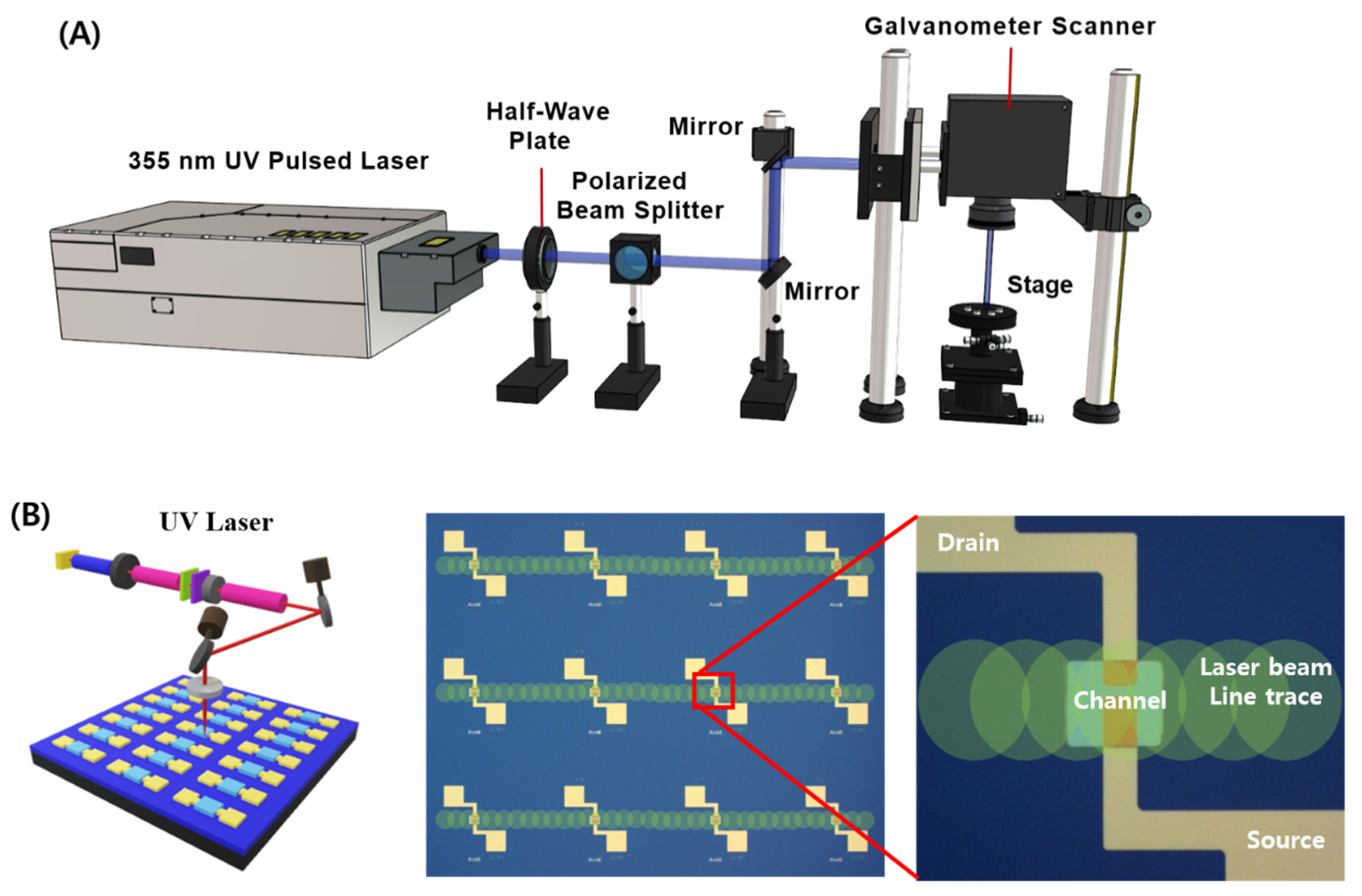
Figure 2.
Transfer characteristics of a-IGZO TFTs after a 355 nm UV pulsed laser annealing process for a laser beam energy (a) from pristine (no annealing) to 90 mW and (b) from 119 mW to 280 mW. Output characteristics of a-IGZO TFT after a 355 nm UV pulsed laser annealing process for a laser beam energy of (c) pristine, (d) 55 mW, and (e) 77 mW.
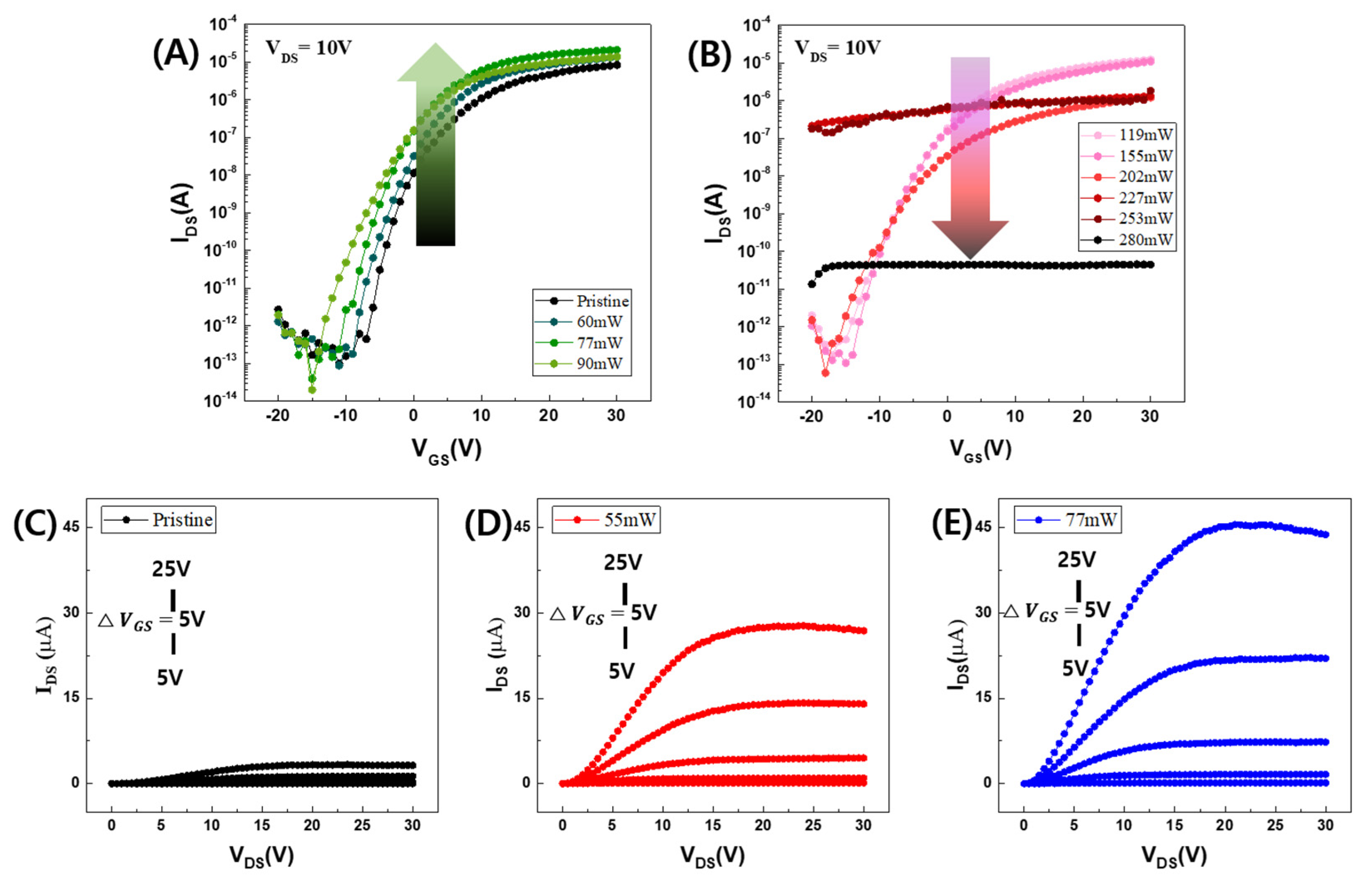
Figure 3.
Threshold voltages (VTH) of a-IGZO TFTs after a 355 nm UV pulsed laser annealing process for a laser beam energy ranging from pristine (no annealing) to 280 mW.
Figure 3.
Threshold voltages (VTH) of a-IGZO TFTs after a 355 nm UV pulsed laser annealing process for a laser beam energy ranging from pristine (no annealing) to 280 mW.
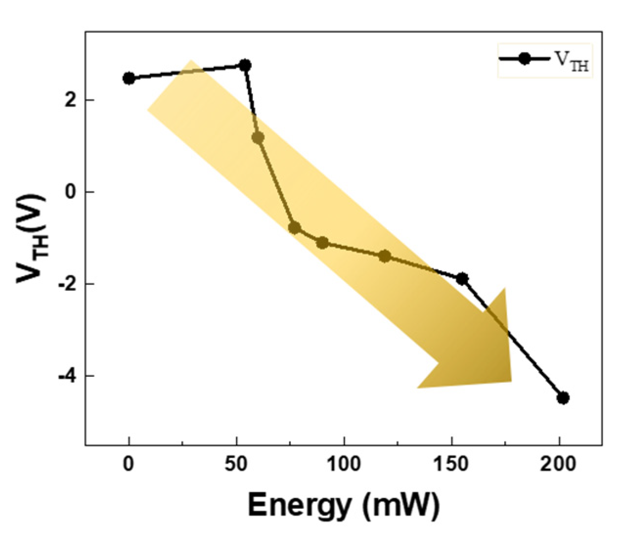
Figure 4.
Scanning electron microscopy (SEM) images of a-IGZO TFTs after a 355 nm UV pulsed laser annealing process for the laser beam energies of (a) pristine (no annealing), (a) 77 mW, and (c) 227 mW. In case of the high energy of 227 mW, laser beam line traces are investigated.
Figure 4.
Scanning electron microscopy (SEM) images of a-IGZO TFTs after a 355 nm UV pulsed laser annealing process for the laser beam energies of (a) pristine (no annealing), (a) 77 mW, and (c) 227 mW. In case of the high energy of 227 mW, laser beam line traces are investigated.
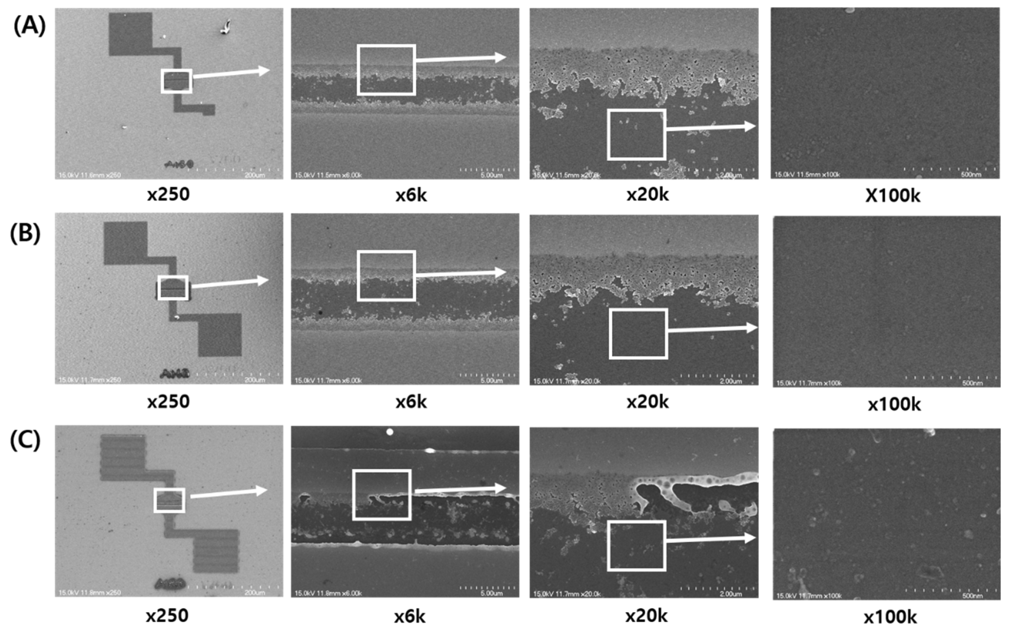
Figure 5.
(a) Transmittance and (b) absorbance of a-IGZO thin films annealed using a 355 nm UV pulsed laser for laser beam energies of 0 (pristine), 60, 120, and 280 mW.
Figure 5.
(a) Transmittance and (b) absorbance of a-IGZO thin films annealed using a 355 nm UV pulsed laser for laser beam energies of 0 (pristine), 60, 120, and 280 mW.
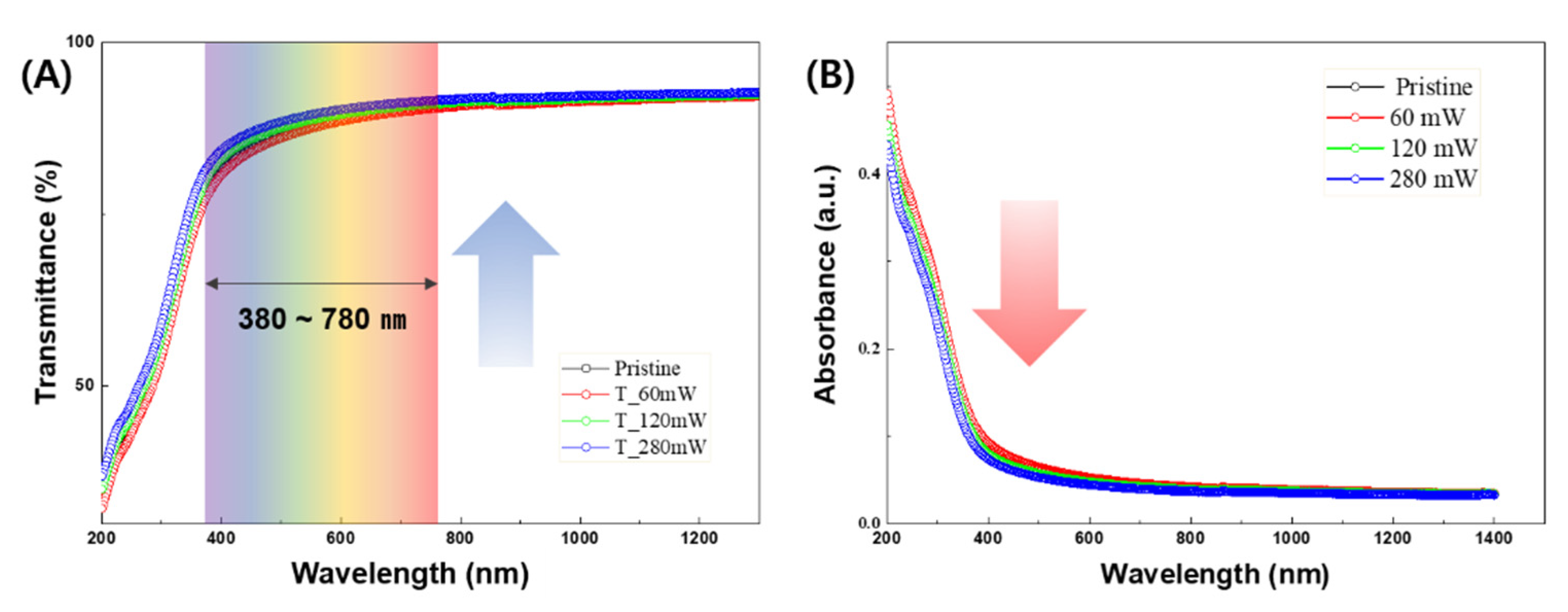
Figure 6.
Tauc Plot for the energy band gap of a-IGZO thin films shown in Figure 5. The 355 nm UV pulsed laser beam energies are (a) 0 (pristine), (b) 60, (c) 120, and (d) 280 mW.
Figure 6.
Tauc Plot for the energy band gap of a-IGZO thin films shown in Figure 5. The 355 nm UV pulsed laser beam energies are (a) 0 (pristine), (b) 60, (c) 120, and (d) 280 mW.
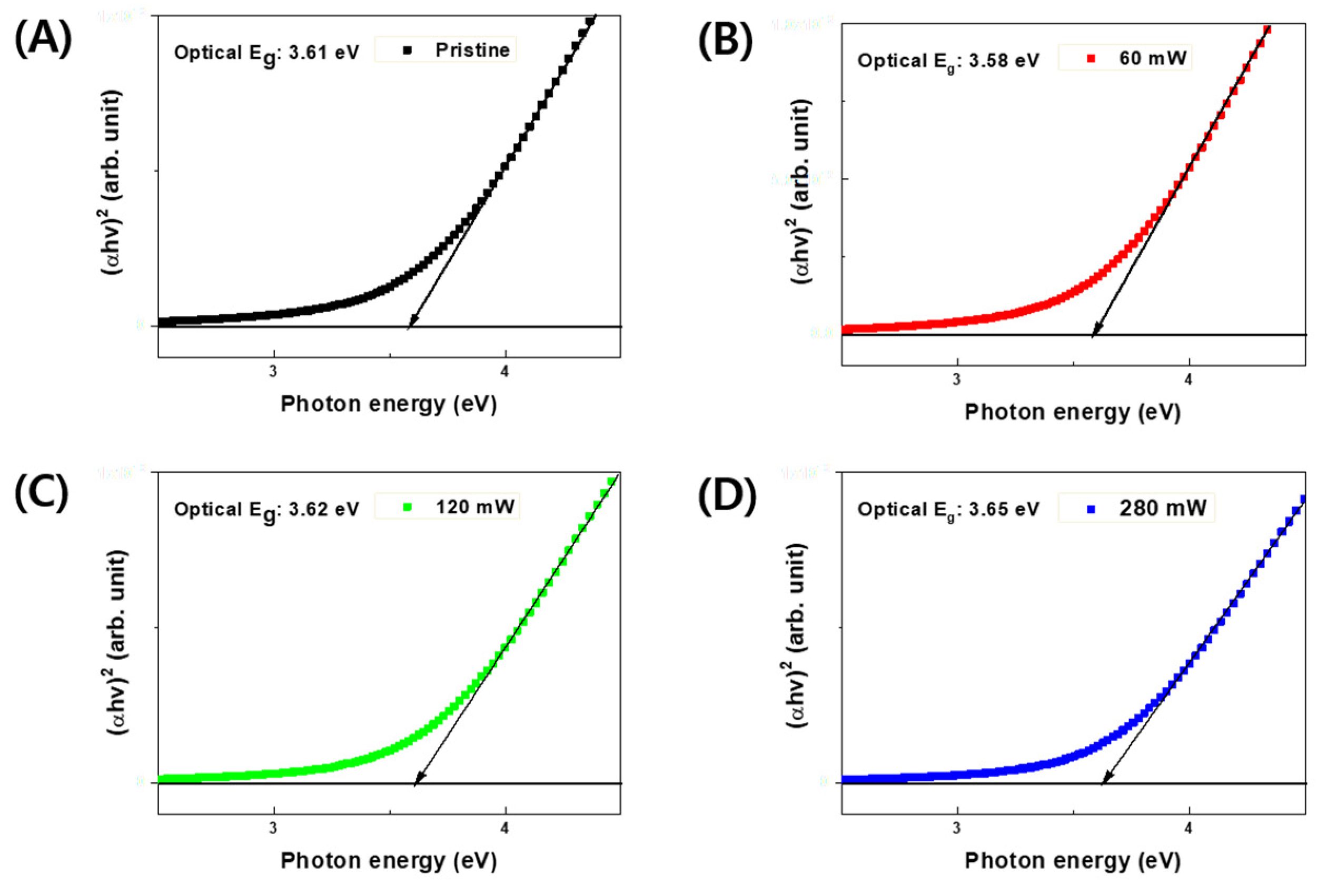
Figure 7.
(a) Ultraviolet photoelectron spectroscopy (UPS) spectrum of 355 nm UV pulsed laser annealed a-IGZO thin films for direct determination of (b) cutoff energy and (c) valence band maximum (VBM).
Figure 7.
(a) Ultraviolet photoelectron spectroscopy (UPS) spectrum of 355 nm UV pulsed laser annealed a-IGZO thin films for direct determination of (b) cutoff energy and (c) valence band maximum (VBM).
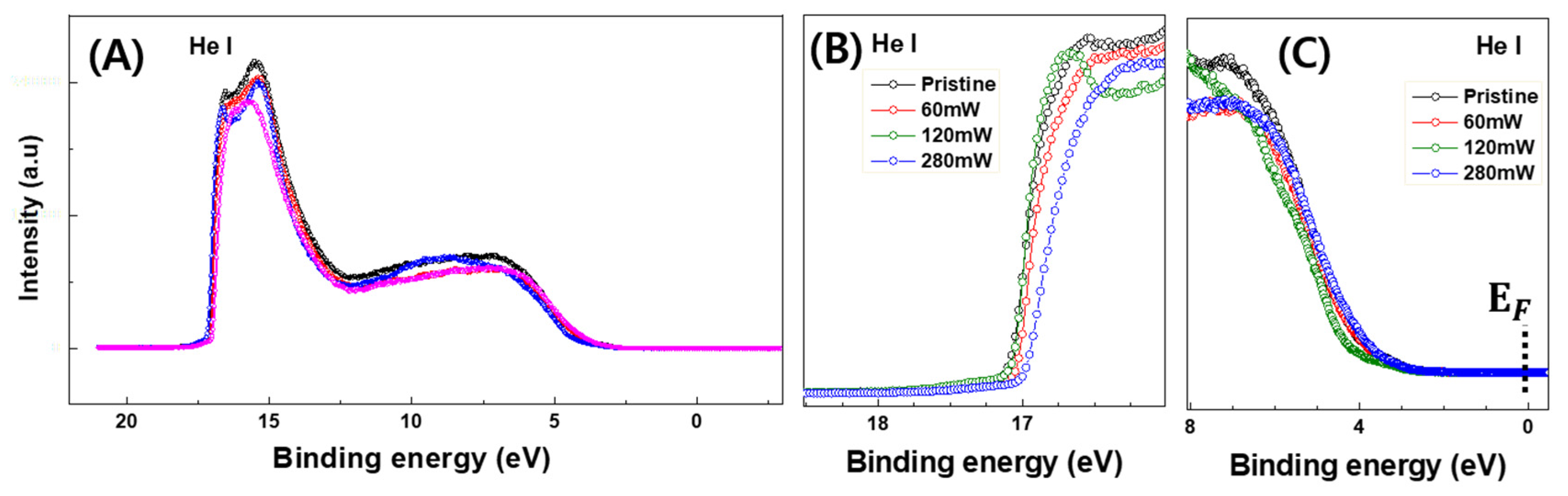
Figure 8.
Energy band diagrams of (a) a-IGZO thin films and (b) a-IGZO/ITO junction structures extracted from the UPS results shown in Figure 7.
Figure 8.
Energy band diagrams of (a) a-IGZO thin films and (b) a-IGZO/ITO junction structures extracted from the UPS results shown in Figure 7.
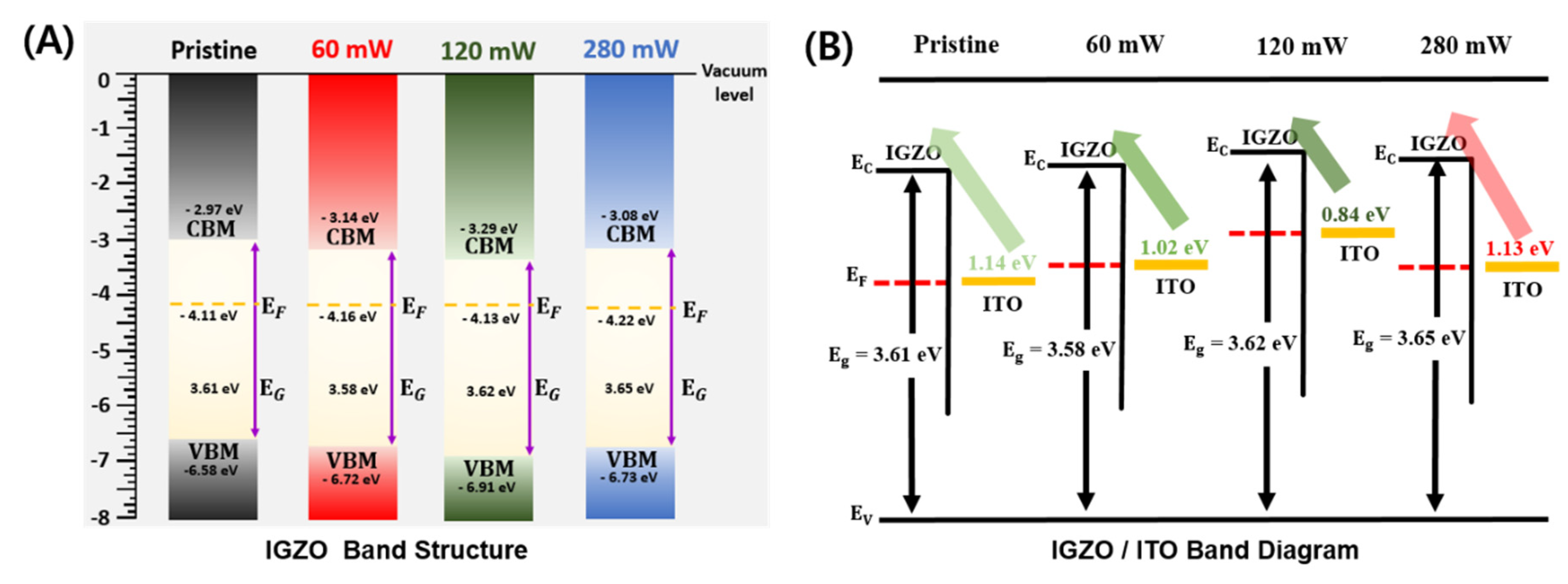

Table 1.
VTH , subthreshold swing (S.S.), mobility (m), and the on/off ratio (Ion/Ioff) for different laser beam energies.
Table 1.
VTH , subthreshold swing (S.S.), mobility (m), and the on/off ratio (Ion/Ioff) for different laser beam energies.
| Laser beam power | VTH [V] | S.S [V/dec] | mn [cm2/V·s] | Ion/Ioff |
|---|---|---|---|---|
| 22 | 4.06ㄸ+ | |||
| 0.84 | ||||
| Pristine | 2.48 2.76 |
2.00 | 0.84 | 4.06E+7 |
| 54 mW 60 |
2.76 | 1.77 | 1.20 | 6.79E+7 1 |
| 60 mW | 1.19 | 1.81 | 0.77 | 1.88E+7 |
| 77 mW | -0.77 | 1.81 | 0.35 | 2.41E+8 |
| 90 mW | -1.10 | 1.61 | 0.30 | 4.84E+8 |
| 119 mW | -1.39 | 1.86 | 1.13 | 2.91E+7 |
| 155 mW | -1.88 | 2.28 | 0.32 | 5.42E+7 |
| 202 mW | -4.47 | 2.64 | 0.03 | 4.62E+6 |
| 227 mW | - | - | - | 3.45E+0 |
| 253 mW | - | - | - | 4.27E+0 |
| 280 mW | - | - | - | 1.36E+1 |
Disclaimer/Publisher’s Note: The statements, opinions and data contained in all publications are solely those of the individual author(s) and contributor(s) and not of MDPI and/or the editor(s). MDPI and/or the editor(s) disclaim responsibility for any injury to people or property resulting from any ideas, methods, instructions or products referred to in the content. |
© 2023 by the authors. Licensee MDPI, Basel, Switzerland. This article is an open access article distributed under the terms and conditions of the Creative Commons Attribution (CC BY) license (http://creativecommons.org/licenses/by/4.0/).
Copyright: This open access article is published under a Creative Commons CC BY 4.0 license, which permit the free download, distribution, and reuse, provided that the author and preprint are cited in any reuse.


