
Submitted:
16 October 2023
Posted:
17 October 2023
You are already at the latest version
Abstract
BiFeO3/La0.7Sr0.3MnO3 (BFO/LSMO) epitaxial heterostructures were successfully synthesized by pulsed laser deposition on (001)-oriented SrTiO3 single crystal substrates with Au top electrodes. Stable bipolar resistive switching characteristics regulated by ferroelectric polarization reversal was observed in the Au/BFO/LSMO heterostructures. The conduction mechanism was revealed to follow the Schottky emission model, and the Schottky barriers in high resistance and low resistance states were estimated based on temperature-dependent current–voltage curves. Further, the observed memristive behavior was interpreted via the modulation effect on the depletion region width and the Schottky barrier height caused by ferroelectric polarization reversal, combining with the oxygen vacancies migration near the BFO/LSMO interface.
Keywords:
resistance switching
; interface
; ferroelectric polarization
; Schottky barrier
1. Introduction
In recent years, nonvolatile resistive switching (RS) behavior has attracted significant attention due to their high speed, low power dissipation and their potential applications in next-generation, ultra-high-density resistance switching random-access memories of simple devices. Conventional binary metal oxides such as TiO2 [1], NiO [2], ZnO [3], CuxO [4], etc., have been frequently used as RS layers in memristors. However, in order to develop high-performance memory devices, ferroelectric thin films are emerging as alternatives to RS layers. Polarization switching characteristics provide new degrees of freedom to manipulate the RS behavior. They also provide a rectification current–voltage behavior, and thus reduce sneak currents in crossbar resistive random-access memory devices [5]. Ferroelectric thin films, including BTO [6], 30% Sr-doped BaTiO3 [7], 5% Al0.5Nb0.5O3-doped Pb(Zr0.52Ti0.48)O3 (PZT) [8], BiFeO3 (BFO) [9,10,11,12], Ca-doped BiFeO3 [13], and Hf0.93Y0.07O2 [14], have been investigated as the RS layer. With emerging manipulation methods, various interpretations have been proposed to understand the ferroelectric resistance switching behavior, such as the conductive filaments model [15], trapping/detrapping of the free charges and the migration of the oxygen vacancies [7], and polarization-modulated Schottky barriers [16], whereas a clear understanding of the switching mechanisms in ferroelectric memristors is still in face of challenge.
In this work, we prepared an epitaxial BFO/LSMO heterostructure as the RS layer, and studied the RS behavior by measuring the temperature-dependent current–voltage properties and calculating the conduction barriers. A model of ferroelectric polarization reversal modulation combining the migratory effect of the oxygen vacancies near the BFO/LSMO interface has been proposed to interpret the RS mechanism.
2. Experimental
BFO films of 150 nm thick were epitaxially grown on (001) SrTiO3 single-crystal substrates buffered with LSMO thin films as the bottom electrode. Both BFO and LSMO were prepared by a pulsed laser deposition technique with a 248 nm KrF excimer laser. BFO and LSMO were grown at 690 °C and 750 °C under oxygen pressures of 15 and 16 Pa, respectively. Further in situ post-annealing under a 3000 Pa oxygen partial pressure was conducted for 30 min. The phase structure was studied by X-ray diffraction (XRD; Bruker D8 Discover) using CuKα1 radiation (λ = 1.5406 Å). The ferroelectric polarization-electric field hysteresis loops were measured on a ferroelectric tester (Precision II, Radiant Technologies, USA). The local piezoresponse was measured by piezoelectric force microscopy (PFM, MFP-3D, Oxford, USA). Current–voltage curves were recorded on a Keithley 2450 source meter (Tektronix Inc., USA) using Au discs as the top electrodes.
3. Results and Discussion
Figure 1 shows a typical XRD θ-2θ pattern for the as-prepared BFO/LSMO heterostructures on the (001) STO substrate. Only (00l)-type reflections are observed, indicating predominant (001) growth along the orientation of the substrate.
Figure 2a displays the typical morphology of a cross-section of a BFO/LSMO heterostructure. The thickness of the BFO layer was measured to be about 150 nm. One can observe a sharp, smooth interface between the BFO/LSMO film and the STO substrate. Figure 2b shows selected area electron diffraction (SAED) patterns along the [100] c zone axis, taken from the BFO layer. The reflection patterns were indexed based on pseudo-cubic unit cells of BFO. The interface structures of LSMO/STO and BFO/LSMO have been illustrated by the high-resolution TEM images as shown in Figure 3c,d. One can see that the interface is coherent, without any misfit dislocations near the interface, indicating the high epitaxy and crystallinity of the BFO and LSMO films. The spacings of the lattice fringes from two directions were measured as 0.392 nm and 0.403 nm in Figure 2c, corresponding to the (001) and (010) planes of pseudo-cubic BiFeO3, respectively. Combining the diffraction and high resolution results, the epitaxial relationships between the film
and the substrate can be determined to be (001) BFO//(001) LSMO//(001) STO and [010] BFO//[010] LSMO//[010] STO, which is consistent with the XRD results.
Figure 3a presents an AFM topography image of the BFO film on a 4 μm × 4 μm scale. The BFO film is smooth, and the root mean square roughness was measured to be 1.2 nm. The local piezoelectric response of the BFO thin film were studied by piezoelectric force microscopy, and the piezoresponse phase–voltage hysteresis loops and the butterfly-shaped amplitude–voltage curves are shown in Figure 3b. The apparent 180° phase flip in the phase–voltage loops confirmed the domain switching of the BFO film, while dips in the amplitude–voltage curves at −0.8 V and 1.4 V correspond to the coercive voltages of BFO films in the heterostructure. The asymmetric coercive voltages may result from the built-in fields [17,18] or the contact barriers between the ferroelectric films and the top as well as bottom electrodes [19]. Figure 3c shows the P–E hysteresis loops of the BFO film under various applied voltages. The hysteresis loops are square-like and saturated, with a polarization of 61.2 μC/cm2 and a coercive field of 171.6 kV/cm, revealing the high quality of the as-prepared BFO film.
A typical current–voltage (I-V) curve for the Au/BFO/LSMO heterostructure is shown in Figure 4a. I–V curves were measured by four continuous voltage sweeping sequence cycles of 0 → +3 → 0 → –3 → 0 V without an initial electrical forming process. The observed I – V curves exhibited typical hysteresis features and a bipolar resistance state effect. In the positive voltage sweeping cycle (0 → +3 → 0 V), the heterostructure changed from a high-resistance (HR) state to a low-resistance (LR) state, whereas it changed from an LR state to a HR state during the negative voltage sweeping cycle (0 → –3 → 0 V). The resistances of the HR and LR states remained unchanged, with a steady RH/RL ratio of 10 after continuously writing/reading over 100 cycles, revealing superior fatigue characteristics, as shown in Figure 4b.
To further understand the physical resistive switching mechanism, the conductive transport behaviors of the Au/BFO/LSMO heterostructure were determined. Possible conducting models, such as space-charge-limited conduction (SCLC), Poole–Frenkel emission (PF) and Schottky emission (SE), were used to fit the I–V data [20]. The best fit resulted from use of the Schottky emission model [21,22], which is described by
where A is the Richardson constant, Φ is the Schottky barrier height, εr is the dielectric constant of the film and d is the sample thickness. As shown in Figure 5, linear relationships between lnJ and V1/2 indicate that the Schottky barrier controls the conductive behavior of the BFO film. In the HR state branch, linear fitting is suitable within the applied voltage range, while in the LR state branch, a linear relationship was observed in the low voltage range of 0 - 1.36 V.
Figure 6a,d show the temperature dependence of the I–V curves in the range of 100 K-500 K. To further calculate the activation energy () and Schottky barrier Φ, the logarithmic of current density (ln(J/T2)) was plotted against reversal temperature (1000/T) at various applied voltages, which are shown in Figure 6b,e. The activation energy was calculated to be 0.53-0.6 eV for the HR state, while it was 0.52-0.67 eV for LR state. These activation energy values are identical to the activation energy of oxygen vacancies in ferroelectric oxides [23]. Furthermore, the activation energies were replotted against the square root of voltage, as shown in Figure 6c,f. The effective barrier heights between the film and electrode were calculated as 0.43 eV and 1.18 eV for the LR and HR states, respectively.
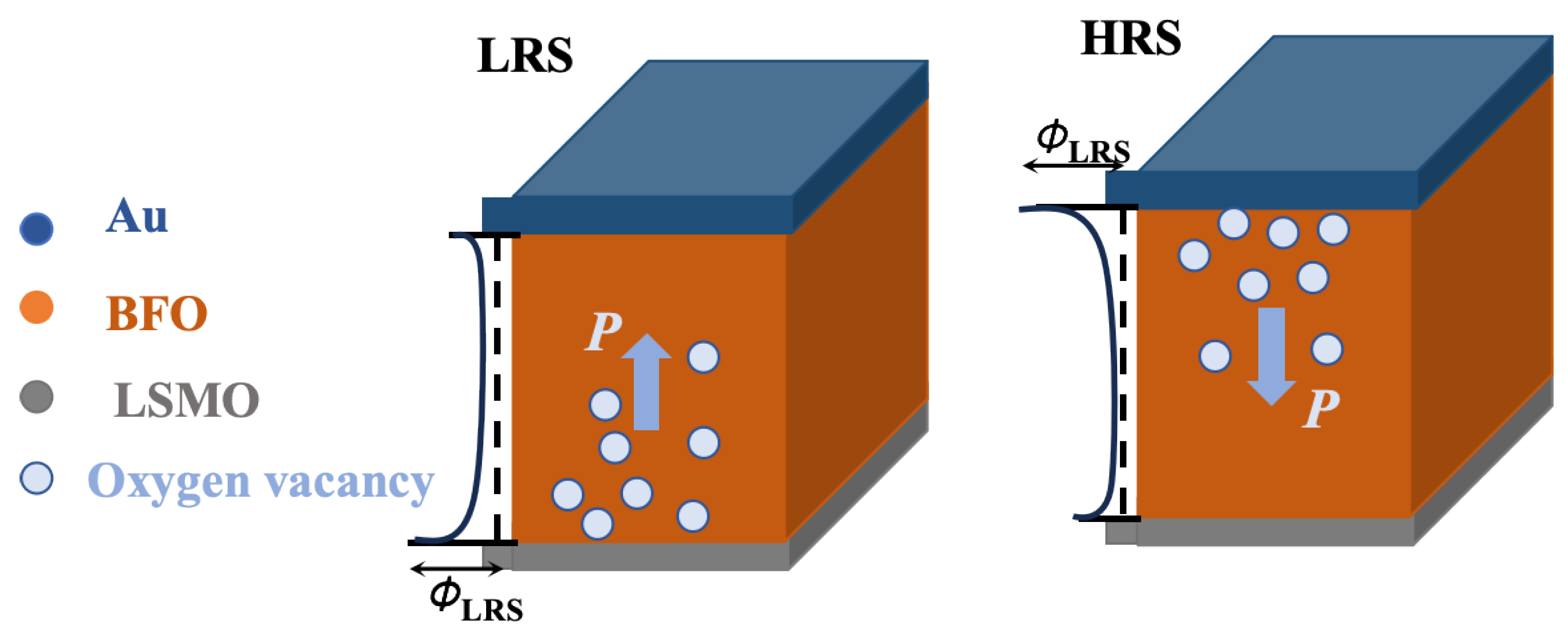
According to the above results, the resistive switching properties in the BFO/LSMO heterostructure can be interpreted by considering the modulation effect on the depletion width and the potential barrier height via ferroelectric polarization reversal, along with the oxygen vacancies migration near the BFO/LSMO interface [24,25]. The work functions of LSMO and Au are 4.7 eV and 5.1 eV, respectively [26,27], while the work function, electron affinity and energy band gap of BFO are 4.7 eV, 3.3 eV, and 2.8 eV, respectively [27,28]. Thus, the nominal Schottky barrier heights for the Au/BFO and the LSMO/BFO contacts can be estimated as 1.8 eV and 1.5 eV, respectively. However, one may also note that the ferroelectric polarization also plays a key role in controlling the transport properties of metal/ferroelectric/metal structures.
As shown in the schematic diagrams in Figure 7, with upward polarization, the downward depolarization field induces the electrons accumulation near the BFO/LSMO interface, reducing the width depletion region on the BFO side and thus the barrier height. Additionally, with upward polarization in the BFO layer, the Schottky barrier at the BFO/LSMO interface is the dominating factor in controlling the transport property in the Au/BFO/LSMO heterostructure. When applying a positive bias voltage, the polarization was switched downwards and the carriers were trapped near the Au/BFO interface, which then enhanced the barrier near the top Au/BFO interface. Therefore, the resistance of the heterostructure with upward polarization (downward polarization) is in an LR (HR) state. Furthermore, oxygen vacancies are frequently observed in BFO thin films [29,30] and the migration and distribution of oxygen vacancies also lead to band-bending and further increases in the Schottky barrier height. As shown in the schematic in Figure 7, oxygen vacancies drift toward and accumulate at the BFO/LSMO and Au/BFO interface for upwards and downwards polarization, respectively, which further enhances the Schottky barrier height for each interface, leading to LR and HR states, respectively. The proposed scenario was confirmed by the above I–V curve fitting, as well as the calculated Schottky barrier values of 0.43 eV and 1.18 eV for the LRS and HRS in Figure 6, respectively.
4. Conclusions
In summary, we have reported ferroelectric-related resistive switching phenomena in a Au/BFO/LSMO heterostructure. Stable bipolar resistive switching behavior has been confirmed by I–V hysteresis loops. The conduction mechanism was revealed to follow the Schottky emission model and effective Schottky barriers of 0.43 eV and 1.18 eV under HR and LR states were estimated based on temperature-dependent current–voltage curves. The observed resistive switching characteristics was determined by the modulation effect on the depletion region width and the potential barrier height via ferroelectric polarization reversal, along with the oxygen vacancies migration at the BFO/LSMO and Au/BFO interfaces.
Author Contributions
Conceptualization, H.Q. and W.W.; methodology, W.W. and H.Q.; software, H.Q.; formal analysis, H.Q. and X.C.; investigation, H.Q., X.C. and W.W.; resources, W.W.; data curation, H.Q.; writing—original draft preparation, W.W. and H.Q.; writing—review and editing, X.C.; supervision, X.C.; project administration, H.Q.; funding acquisition, H.Q. All authors have read and agreed to the published version of the manuscript.
Funding
This work was funded by the National Natural Science Foundation of China, grant number 12104140.
Institutional Review Board Statement
Not applicable.
Informed Consent Statement
Not applicable.
Data Availability Statement
The data presented in this study are available on request from the corresponding author.
Conflicts of Interest
The authors declare that they have no known competing financial interests or personal relationships that could have appeared to influence the work reported in this paper.
References
- Kwon, D.H.; Kim, K.M.; Jang, J.H.; Jeon, J.M.; Lee, M.H.; Kim, G.H.; Li, X.S.; Park, G.S.; Lee, B.; Han, S.; Kim, M.; Hwang, C.S. Atomic structure of conducting nanofilaments in TiO2 resistive switching memory. Nat. Nanotechnol. 2010, 5, 148–153. [Google Scholar] [CrossRef]
- Kim, D.C.; Seo, S.; Ahn, S.E.; Suh, D.S.; Lee, M.J.; Park, B.H.; Yoo, I.K.; Baek, I.G.; Kim, H.J.; Yim, E.K.; Lee, J.E.; Park, S.O.; Kim, H.S.; Chung, U.I.; Moon, J.T.; Ryu, B.I. Electrical observations of filamentary conductions for the resistive memory switching in NiO films. Appl. Phys. Lett. 2006, 88, 202102–202102-3. [Google Scholar] [CrossRef]
- Ren, S.X.; Zhang, L.Y.; Dong, J.Y.; Huang, Y.F.; Guo, J.J.; Zhang, L.; Zhao, J.; Zhao, X.; Chen, W. Electric field control of magnetism in Ti/ZnO/Pt and Ti/ZnO/SRO devices. J. Mater. Chem. C 2015, 3, 4077–4080. [Google Scholar] [CrossRef]
- Dong, R.; Lee, D.S.; Xiang, W.F.; Oh, S.J.; Seong, D.J.; Heo, S.H.; Choi, H.J.; Kwon, M.J.; Seo, S.N.; Pyun, M.B.; Hasan, M.; Hwang, H. Reproducible hysteresis and resistive switching in metal-CuxO-metal heterostructures. Appl. Phys. Lett. 2007, 90, 042107. [Google Scholar] [CrossRef]
- Zackriya, V.M.; Kittur, H.M.; Chin, A. A novel read scheme for large size one-resistor resistive random access memory array. Sci. Rep. 2017, 7, 42375. [Google Scholar] [CrossRef]
- Cao, Y.; Shen, J.; Randall, C.A.; Chen, L.Q. Phase-field modeling of switchable diode-like current-voltage characteristics in ferroelectric BaTiO3. Appl. Phys. Lett. 2014, 104, 182905. [Google Scholar] [CrossRef]
- Zou, X.; Ong, H.G.; You, L.; Chen, W.G.; Ding, H.; Funakubo, H.; Chen, L.; Wang, J.L. Charge trapping-detrapping induced resistive switching in Ba0.7Sr0.3TiO3. AIP Adv. 2012, 2, 032166. [Google Scholar] [CrossRef]
- Bourim, E.M.; Park, S.; Liu, X.J.; Biju, K.P.; Hwang, H.; Ignatiev, A. Ferroelectric polarization effect on Al-Nb codoped Pb(Zr0.52Ti0.48)O3/Pr0.7Ca0.3MnO3 heterostructure resistive memory. Electrochem. Solid-State Lett. 2011, 14, H225. [Google Scholar] [CrossRef]
- Wang, C.; Jin, K.J.; Xu, Z.T.; Wang, L.; Ge, C.; Lu, H.B.; Guo, H.Z.; He, M.; Yang, G.Z. Switchable diode effect and ferroelectric resistive switching in epitaxial BiFeO3 thin films. Appl. Phys. Lett. 2011, 98, 192901. [Google Scholar] [CrossRef]
- Yao, Y.B.; Zhang, B.; Chen, L.; Yang, Y.; Wang, Z.H.; Alshareef, H.N.; Zhang, X.X. Polarization-tuned diode behaviour in multiferroic BiFeO3 thin films. J. Phys. D: Appl. Phys. 2013, 46, 055304. [Google Scholar] [CrossRef]
- Chen, D.X.; Li, A.D.; Wu, D. Resistive switching inBiFeO3-based heterostructures due to ferroelectric modulation on interface Schottky barriers. J. Mater. Sci.: Mater. Electron. 2014, 25, 3251–3256. [Google Scholar]
- Choi, T.; Lee, S.; Choi, Y.J.; Kiryukhin, V.; Cheong, S.W. Switchable ferroelectric diode and photovoltaic effect in BiFeO3. Science 2009, 324, 63–66. [Google Scholar] [CrossRef]
- Yang, C.H.; Seidel, J.; Kim, S.Y.; Rossen, P.B.; Yu, P.; Gajek, M.; Chu, Y.H.; Martin, L.W.; Holcomb, M.B.; He, Q.; Maksymovych, P.; Balke, N.; Kalinin, S.V.; Baddorf, A.P.; Basu, S.R.; Scullin, M.L.; Ramesh, R. Electric modulation of conduction in multiferroic Ca-doped BiFeO3 films. Nat. Mater. 2009, 8, 485–493. [Google Scholar] [CrossRef] [PubMed]
- Müller, M.L.; Becker, M.T.; Strkalj, N.; MacManus-Driscoll, J.L. Schottky-to-Ohmic switching in ferroelectric memristors based on semiconducting Hf0.93Y0.07O2 thin films. Appl. Phys. Lett. 2022, 121, 093501. [Google Scholar] [CrossRef]
- Li, M.; Zhuge, F.; Zhu, X.J.; Yin, K.B.; Wang, J.Z.; Liu, Y.W.; He, C.L.; Chen, B.; Li, R.W. Nonvolatile resistive switching in metal/La-doped BiFeO3/Pt sandwiches. Nanotechnology 2010, 21, 425202. [Google Scholar] [CrossRef]
- Lee, D.; Baek, S.H.; Kim, T.H.; Yoon, J.G.; Folkman, C.M.; Eom, C.B.; Noh, T.W. Polarity control of carrier injection at ferroelectric/metal interfaces for electrically switchable diode and photovoltaic effects. Phys. Rev. B 2011, 84, 125305. [Google Scholar] [CrossRef]
- Cornelius, T.W.; Mocuta, C.; Escoubas, S.; Merabet, A.; Texier, M.; Lima, E.C.; Araujo, E.B.; Kholkin, A.L.; Thomas, O. Piezoelectric response and electrical properties of Pb(Zr1-xTix)O3 thin films: the role of imprint and composition. J Appl Phys. 2017, 122, 164104. [Google Scholar] [CrossRef]
- Gruverman, A.; Kholkin, A.; Kingon, A.; Tokumoto, H. Asymmetric nanoscale switching in ferroelectric thin films by scanning force microscopy. Appl Phys Lett. 2001, 78, 2751–2753. [Google Scholar] [CrossRef]
- Damjanovic, D. Ferroelectric, dielectric and piezoelectric properties of ferroelectric thin films and ceramics. Rep Prog Phys. 1998, 61, 1267–1324. [Google Scholar] [CrossRef]
- Pabst, G.W.; Martin, L.W.; Chu, Y.H.; Ramesh, R. Leakage mechanisms in BiFeO3 thin films. Appl. Phys. Lett. 2007, 90, 072902. [Google Scholar] [CrossRef]
- Scott, J.F. Ferroelectric memories; Springer: Berlin, Germany, 2000. [Google Scholar]
- Sze, S.M. Physics of semiconductor devices, 2nd ed.; Wiley: New York, NY, USA, 1981. [Google Scholar]
- Scott, J.F. Device physics of ferroelectric thin-film memories. Jpn. J. Appl. Phys. 1999, 38, 2272–2274. [Google Scholar] [CrossRef]
- Watanabe, Y. Electrical transport through Pb(Zr,Ti)O3 p-n and p-pheterostructures modulated by bound charges at a ferroelectric surface: Ferroelectric p-n diode. Phys. Rev. B 1999, 59, 11257–11266. [Google Scholar] [CrossRef]
- Meyer, R.; Waser, R. Hysteretic resistance concepts in ferroelectric thin films. J. Appl. Phys. 2006, 100, 051611. [Google Scholar] [CrossRef]
- Wang, L.; Jin, K.J.; Ge, C.; Wang, C.; Guo, H.Z.; Lu, H.B.; Yang, G.Z. Electro-photo double modulation on the resistive switching behavior and switchable photoelectric effect in BiFeO3 films. Appl. Phys. Lett. 2013, 102, 252907. [Google Scholar] [CrossRef]
- Wang, C; Jin, K. J.; Xu, Z.T.; Wang, L; Ge, C., Lu, H.B.; Guo, H.Z.; He, M.; Yang, G.Z. Switchable diode effect and ferroelectric resistive switching in epitaxial BiFeO3 thin films. Appl. Phys. Lett. 2011, 98, 192901. [Google Scholar] [CrossRef]
- Clark, S.J.; Robertson, J. Band gap and schottky barrier heights of multiferroic BiFeO3. Appl. Phys. Lett. 2007, 90, 132903. [Google Scholar] [CrossRef]
- Lee, J.H.; Jeon, J.H.; Yoon, C; Lee, S.; Kim, Y.S.; Oh, T.J.; Kim, Y.H.; Park, J.; Song, T.K.; Park, B.H. Intrinsic defect-mediated conduction and resistive switching in multiferroic BiFeO3 thin films epitaxially grown on SrRuO3 bottom electrodes. Appl. Phys. Lett. 2016, 108, 112902. [Google Scholar] [CrossRef]
- Jiang, A.Q.; Wang, C.; Jin, K.J.; Liu, X.B.; Scott, J.F.; Hwang, C.S.; Tang, T.A.; Lu, H.B.; Yang, G.Z. A Resistive Memory in Semiconducting BiFeO3 Thin-Film Capacitors. Adv. Mater. 2011, 23, 1277–1281. [Google Scholar] [CrossRef]
Figure 1.
XRD pattern of the BFO/LSMO heterostructure.
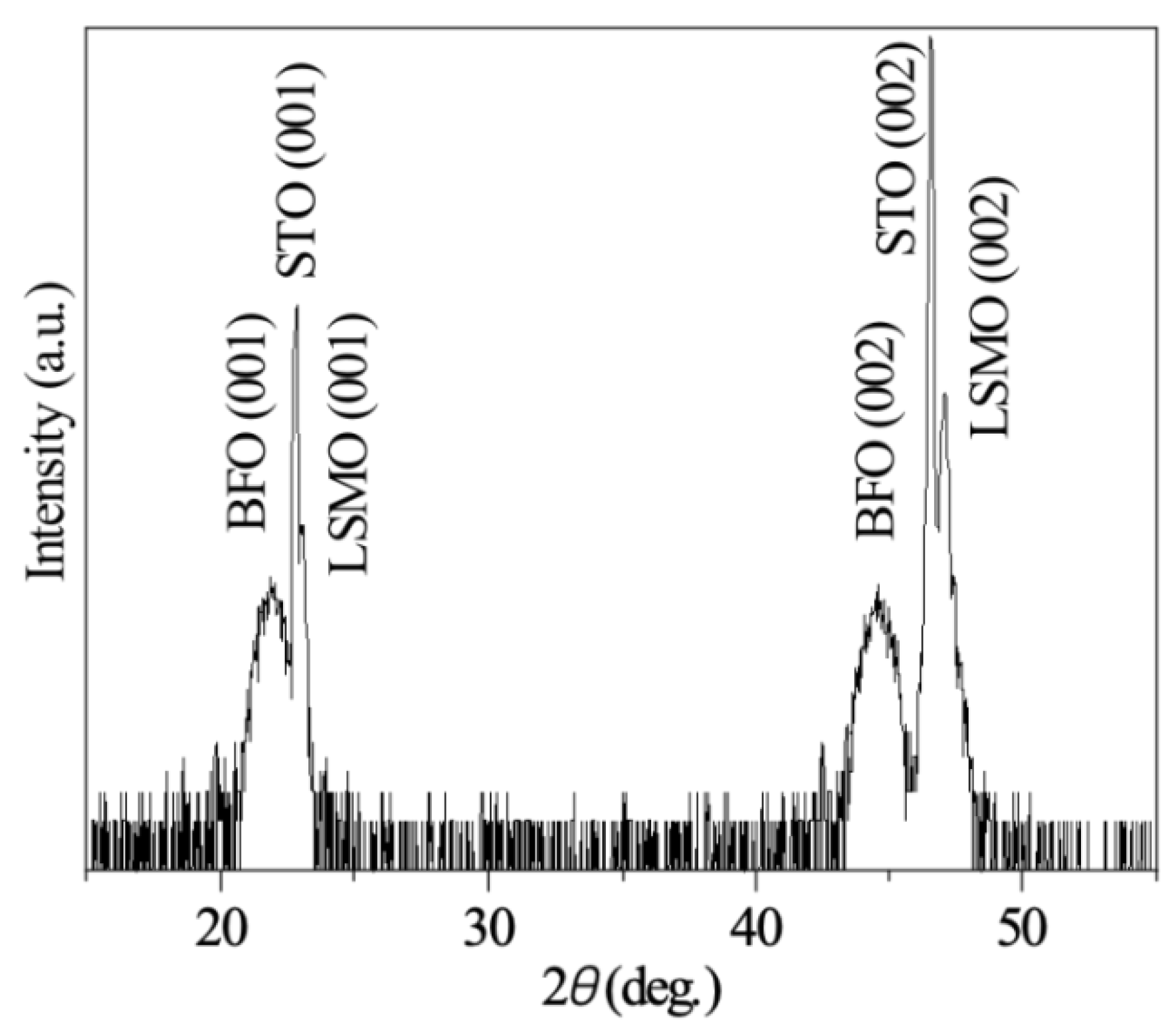
Figure 2.
TEM image (a), SAED (b), HRTEM images near LSMO/STO (c) and BFO/LSMO (d) interface of the BFO/LSMO heterostructure.
Figure 2.
TEM image (a), SAED (b), HRTEM images near LSMO/STO (c) and BFO/LSMO (d) interface of the BFO/LSMO heterostructure.
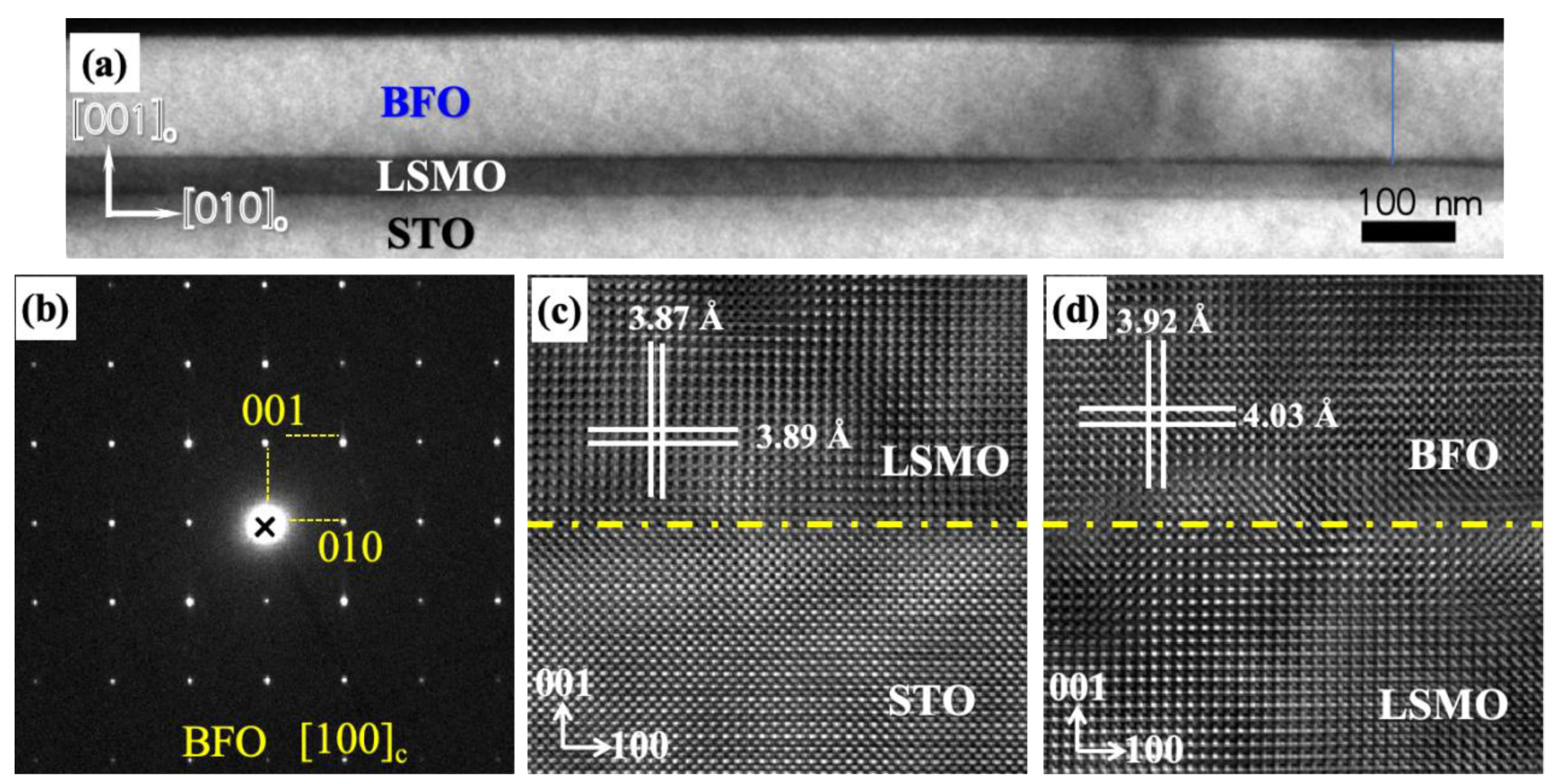
Figure 3.
AFM image (a) of the BFO surface, PFM phase–voltage hysteresis and amplitude–voltage loops (b) and P–E hysteresis loops (c) of BFO films.
Figure 3.
AFM image (a) of the BFO surface, PFM phase–voltage hysteresis and amplitude–voltage loops (b) and P–E hysteresis loops (c) of BFO films.
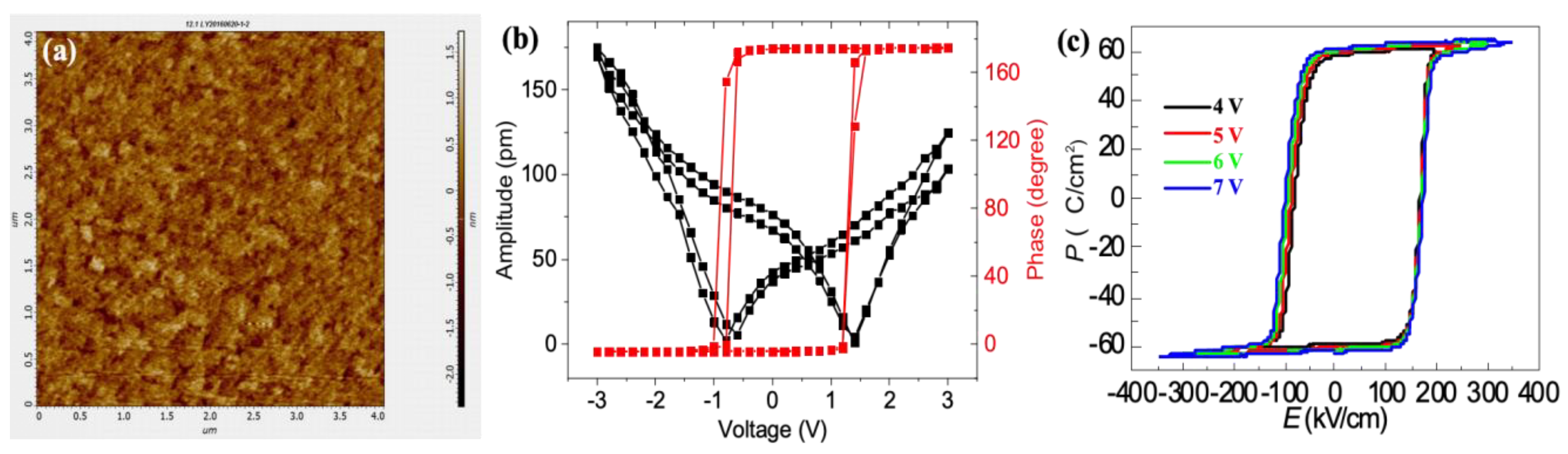
Figure 4.
(a) I–V curve of the BFO/LSMO heterostructure under applied voltages from −3 V to +3 V. (b) Fatigue characteristics of the BFO/LSMO heterostructure.
Figure 4.
(a) I–V curve of the BFO/LSMO heterostructure under applied voltages from −3 V to +3 V. (b) Fatigue characteristics of the BFO/LSMO heterostructure.
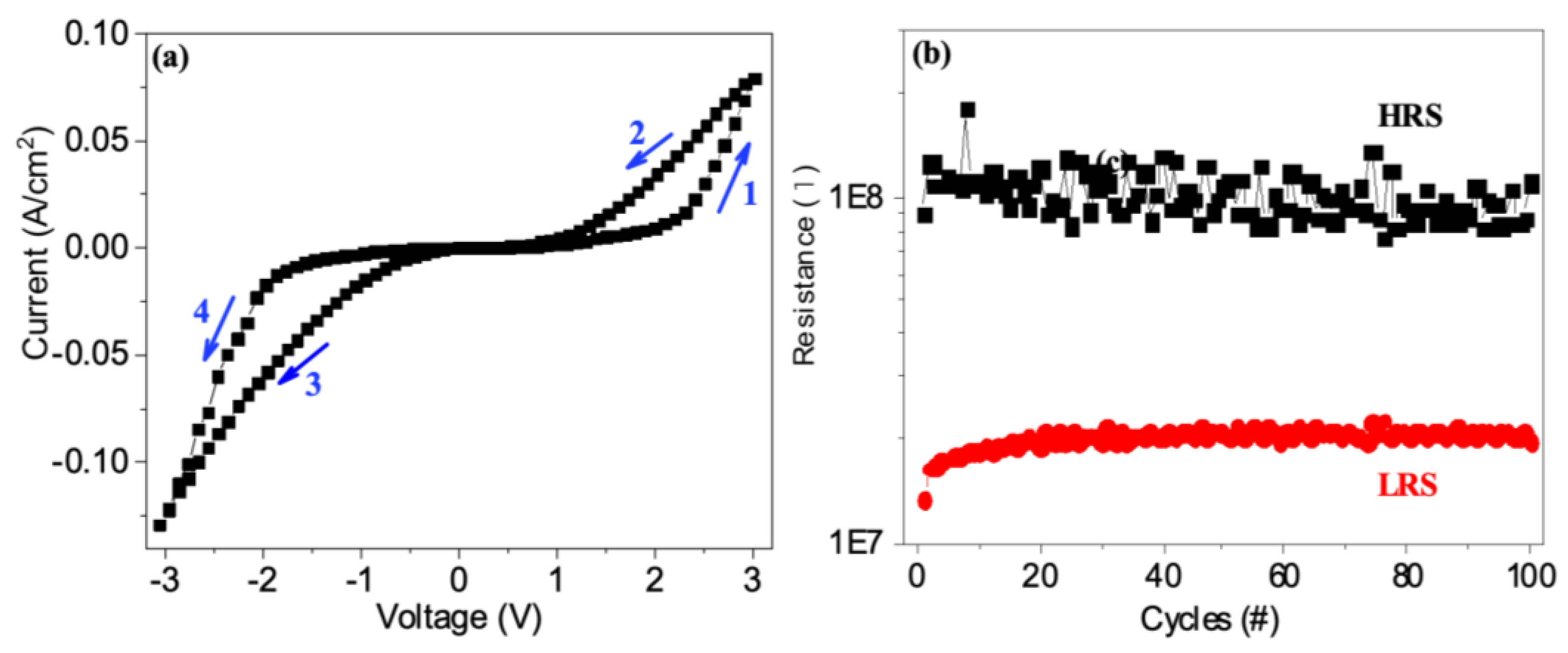
Figure 5.
lnJ vs. V1/2 plots of the BFO/LSMO heterostructure for LRS and HRS under positive and negative voltages.
Figure 5.
lnJ vs. V1/2 plots of the BFO/LSMO heterostructure for LRS and HRS under positive and negative voltages.
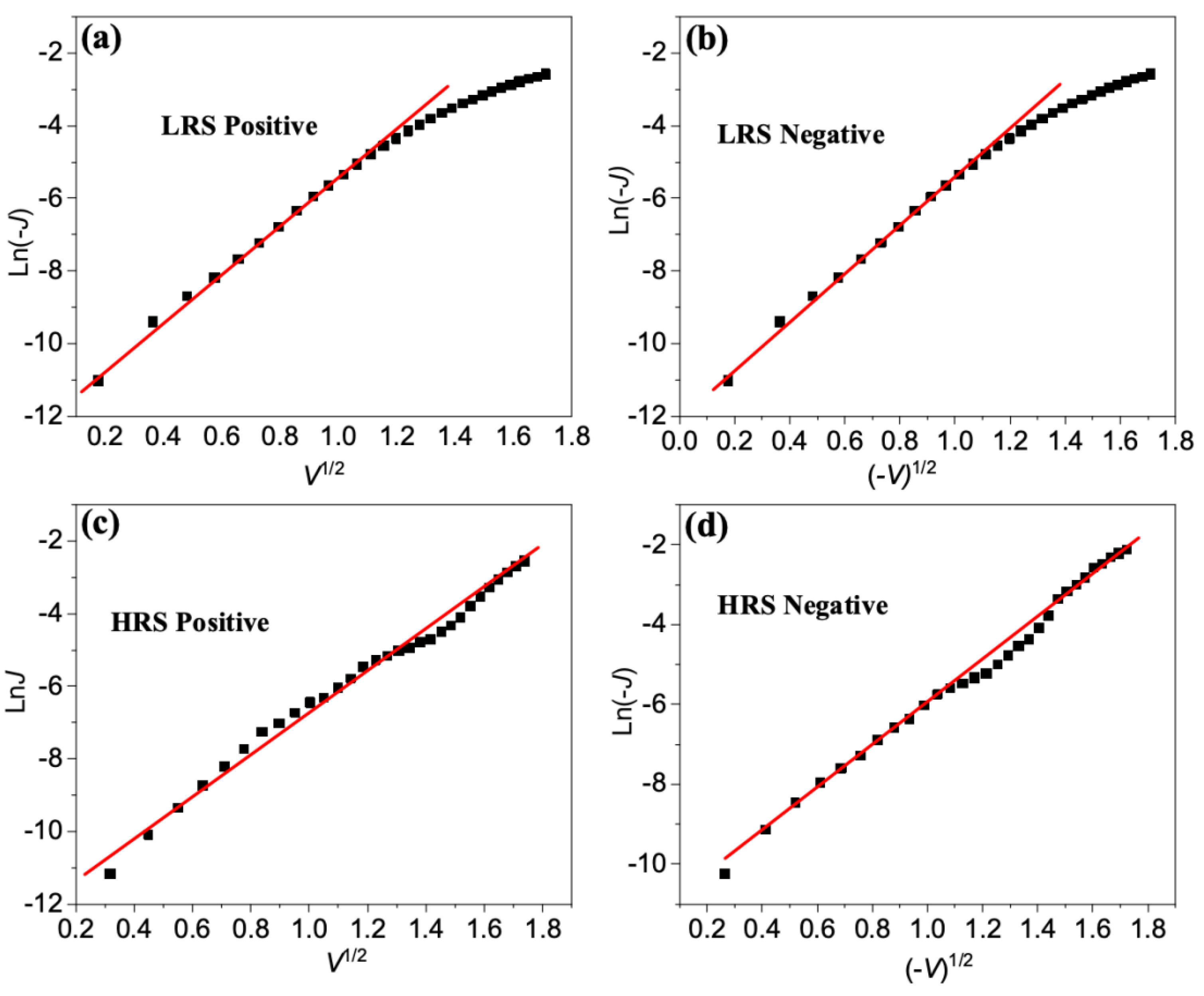
Figure 6.
I–V curves of the BFO/LSMO heterostructure under various temperatures for LRS (a) and HRS (d), ln(J/T2) vs. 1000/T for the BFO/LSMO heterostructure measured at various voltages (b,e), and activation energy as a function of the square root of the voltage for the same film (c,f).
Figure 6.
I–V curves of the BFO/LSMO heterostructure under various temperatures for LRS (a) and HRS (d), ln(J/T2) vs. 1000/T for the BFO/LSMO heterostructure measured at various voltages (b,e), and activation energy as a function of the square root of the voltage for the same film (c,f).
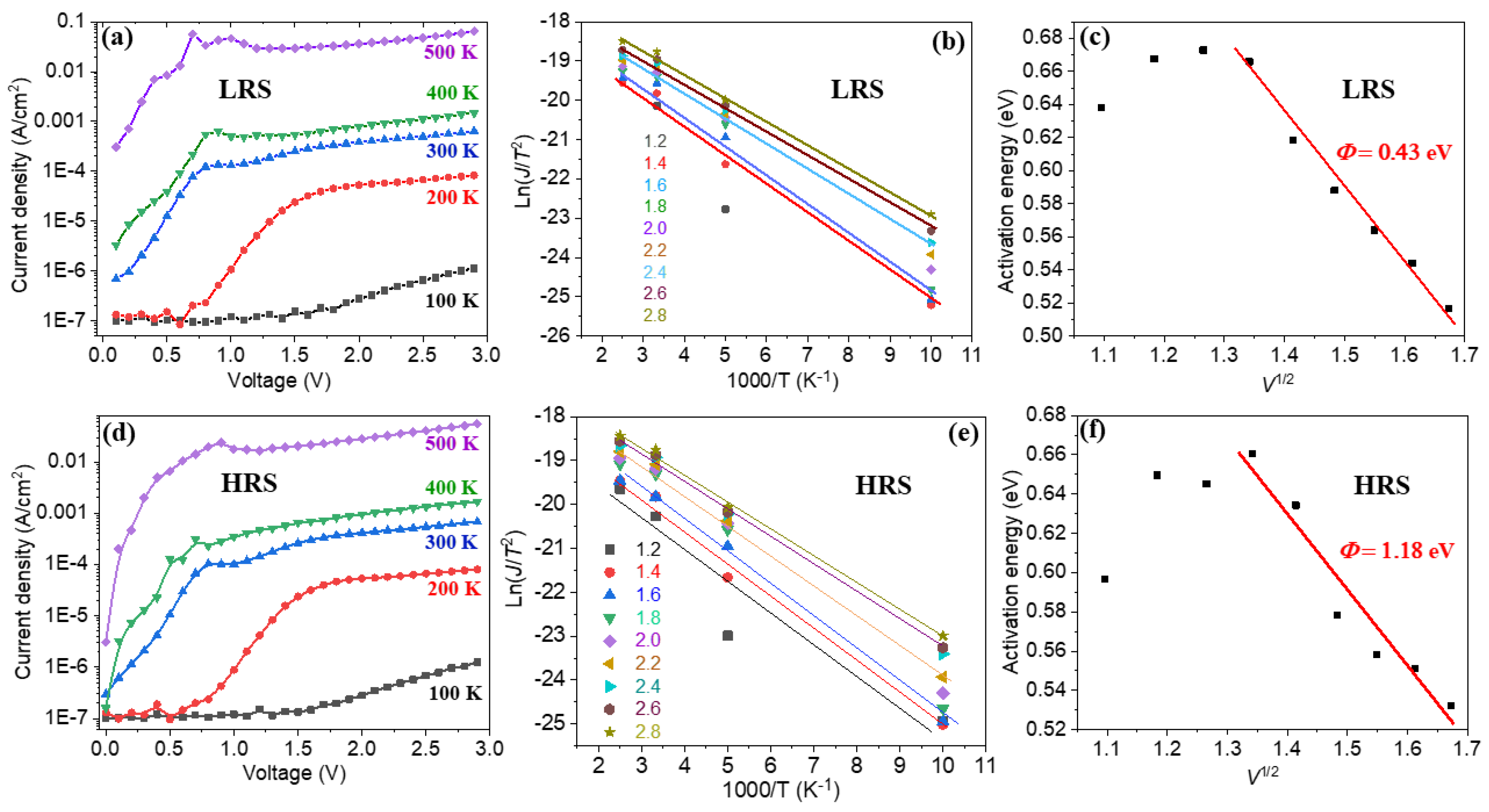
Figure 7.
Schematic diagrams of the Au/BFO/LSMO heterostructure in up and down polarization states.
Disclaimer/Publisher’s Note: The statements, opinions and data contained in all publications are solely those of the individual author(s) and contributor(s) and not of MDPI and/or the editor(s). MDPI and/or the editor(s) disclaim responsibility for any injury to people or property resulting from any ideas, methods, instructions or products referred to in the content. |
© 2024 by the authors. Licensee MDPI, Basel, Switzerland. This article is an open access article distributed under the terms and conditions of the Creative Commons Attribution (CC BY) license (https://creativecommons.org/licenses/by/4.0/).
Copyright: This open access article is published under a Creative Commons CC BY 4.0 license, which permit the free download, distribution, and reuse, provided that the author and preprint are cited in any reuse.


