

Submitted:
10 October 2023
Posted:
10 October 2023
You are already at the latest version
Abstract
Bending waveguide is one of the building blocks of on-chip photonic integrated circuits (PICs). Previous bending waveguides (BWs) usually suffer from larger footprint size in the bending region, which is are not conducive to develop large-scale and high-density PICs. To this end, we propose and numerically investigate an ultra-compact silicon-on-insulator 180-degree waveguide bend with a bending radius of 2 µm. Being different from the previous BWs, the design is based on topologically optimized digital metamaterials, which is implemented by using intelligent genetic algorithms. Simulated results show that the proposed structure has a -1.36 dB bend efficiency per 180-degree at a wavelength of 1.55 µm and occupies a footprint of only 4 × 4 µm2. Moreover, the crosstalk is <−20 dB and the loss is <2.6 dB over a >100 nm operating bandwidth (1.6-1.7 µm) for TE0 modes. With the wide operating bandwidth and ultra-compact footprint, the proposed silicon-based 180-degree waveguide bend shows a potential application as the fundamental component for optical communication interconnect in the ultra-highly integrated photonic circuit.
Keywords:
waveguide
; metamaterials
; algorithm
; silicon photonics
1. Introduction
In the past decades, photonic integrated circuits (PICs) have been leveraging the complementary metal-oxide-semiconductor (CMOS) infrastructure to address the rapidly growing demands for high capacity optical interconnects. It is well known that compact bending waveguide is indispensable for routing the data transmission as well as designing PICs flexibly. Great efforts had been made to achieve sharp waveguide-bends by exploiting photonic crystals [1,2,3,4,5,6,7,8,9,10], plasmonics [11,12,13,14,15,16,17,18,19], and micro-ring resonators [20,21,22]. Waveguide bends based on photonic crystals [1,2,3,4,5,6,7,8,9,10] can exhibit high transmission efficiency. However, the footprint of such devices is very large, since photonic crystals exhibit insufficient localization of the electromagnetic waves.
Moreover, the coupling efficiency between the conventional silicon ridge waveguide and the photonic-crystal waveguide is typically low. Multi-dimensional plasmonic waveguide bends [12,13,14,15,16,17,18,19] have been numerically demonstrated. Unfortunately, these devices suffer not only from large absorption losses from metals, but their fabrication itself is challenging since several alternating metal and dielectric layers are required [3,4,5,6,7,8,9,10]. On the other hand, Xu, et. al. [20,21,22] demonstrated a silicon micro-ring resonator with a radius as small as 1μm. However, the bending losses per 180-degree bend is less than -3 dB and the operating bandwidth is limited in 1nm. Furthermore, they are very sensitive to fabrication errors and therefore, additional compensating mechanisms are required. In addition to these, by using a silver mirror, Ishida, et. al. achieved a 180-degree bending waveguide over an area of ~100 μm × 300 μm with a bend efficiency ~35% [23]. The facet of the mirror has to be ultra-smooth to minimize scattering losses, which complicates the fabrication. AI-Tarawmi and Vogebacher, et. al. have proposed a low loss 180-degree waveguide bend using a slot structure [24] and Euler bend geometry [25], which exhibits a footprint of tens of microns.
One might notice that metamaterials offer a new approach to design compact and power-efficient integrated-photonic devices [26,27,28,29]. By nanostructuring a dielectric (silicon) with features that are smaller than the wavelength, it is possible to engineer the device response to input electromagnetic waves in a manner that allows the device to be much smaller that is otherwise impossible. In previously, by using grating-like structure metamaterials, Xu, et. al. achieved a 180-degree waveguide bending with a bend efficiency of <1 dB [30]. However, the device footprint still over an area of ~60 μm × 100 μm. Therefore, it is highly desirable to explore a 180-degree bending waveguide to ensure various photonic components could be freely stitched on a chip.
In this work, we theoretically study an ultra-compact silicon-based 180-degree waveguide bend based on digital metamaterials. Our method is to design digital metamaterials by utilizing an intelligent genetic algorithm. With such an approach, the local permittivity could be flexibly tailored to explore the desired bending waveguide. The 180-degree waveguide bend with a footprint of only 4 × 4 µm2 and a bend efficiency of -1.36 dB per 180-degree is theoretically demonstrated at a wavelength of 1.55 µm. Moreover, the crosstalk is <−20 dB and the loss is <2.6 dB over a >100 nm operating bandwidth (1.6-1.7 µm) for the TE0 modes operation. With the ultra-compact device footprint and wide operating bandwidth, the designed 180-degree waveguide bend is expected to boost the development of large-scale and high-density PICs.
2. Materials and Methods
In traditional device design, the device structure is given first, then final structure is achieved by the calculated optimization process based on the Maxwell’s equations. To explore the pattern distribution of silicon digital metamaterials structure, inverse design method is introduced. The kernel of “inverse-design” is that the source and target optical fields are given first, then the digital metamaterials structure is built according to the desired input and output optical fields. We implement a binary digital metamaterials structure by discretizing the device area into a number of identical square lattices at sub-wavelength scale. Each lattices can be occupied by silicon or air. More lattices mean that the final structure is more closer to the target structure, while would increase the footprint of the device. To make a tradeoff, we adopt a step-by-step method for the optimization, as Figure 1(a) shows. The geometry of digital metamaterials structure is first set to be square and this region is divided into a number of blocks, such as 100 × 100. After that an optimization genetic algorithms (GA) is utilized to decide the material of each lattices to be silicon or air. The effect ofoptimization is evaluated by a function called figure-of-merit (FOM). If the FOM is lower than the expectation at the end of the optimization, the lattice will be updated by GA operations as a trial for improvement. In detail, the silicon or air lattices are expanded and the optimization process is repeated until the FOM is acceptable or cannot be improved.
As shown in Figure 1, the connection square area (4 × 4 μm2) was partitioned into small lattices (10 nm × 10 nm). This allows the RI for each lattices to be chosen independently. At the second step, the genetic algorithm is implemented to drive an appropriate distribution of RI for pattern area. As a general feature, the refractive indices for the partitioned parts are gene, and the distribution of RI in all areas is used as chromosome for the algorithm. Here, two refractive indices 1 and 2.39 are applied. The refractive indices for sub-areas are determined by the assigned codes. For example, code ‘‘1’’ represents the RI equals to 2.39 (silicon) and code ‘‘0’’ represents 1(air). Then, the first distribution of the RI will be created by the genetic algorithm. At the third and fourth step, as an application, we analyze wave propagation in each lattices population of RI by calculating the transmission at operation wavelength λ=1.5~1.7 μm in the finite-difference timed domain (FDTD) simulation. We defined the figure of merit (FOM) value, which is defined as the normalized transmission of output waveguide, which can be expressed as follow:
where B represents an arbitrary point in the cross-section of the connection area, E0 and H0 represent the basis electric and magnetic fields of the TE0 mode, and E, H denotes the actual electric and magnetic fields at B, respectively. At the last stage, the iterations continue until the FOM cannot be improved or the final FOM is smaller than the expected value. Otherwise, the step which reproduces a new distribution of RI will repeat the cycle. The final structure pattern will be determined and would have the least energy loss when the FOM value reaches the maximum.
3. Results
3.1. Design of 180-degree waveguide bend using digital metamaterials
As shown in Figure 2(a), on-chip silicon-based 180-degree waveguide bend using digital metamaterials is designed based on an intelligent algorithm, which is constructed by combining the genetic algorithm and the finite-difference time-domain (FDTD). The proposed 180-degree waveguide bend structure is consisting of three parts with the digital metamaterials pattern region and input/output waveguide. The width of the input and output single-mode waveguide is chosen to be 1µm. The intelligent genetic algorithm is used to engineer the geometry pattern of the digital metamaterials region. The top-view (xz-plane) schematic diagram of the digital metamaterials pattern region is sketched in Figure 2(b), where the optimization region is chosen to be 4 × 4 μm2 which is discretized intdiscretized into 400 × 400 pixelated lattices. Each lattice diameter is 10 nm and it has a binary state of the material property: silicon or air. The device is designed on a widely used SOI substrate with 220 nm top silicon and 2 μm buried oxide. The proposed 180-degree waveguide bend use free-form digital metamaterials, where the distribution of the silicon and air pixelated lattices is determined using intelligent genetic algorithm. The intelligent algorithm can explore all kinds of structures, and FDTD can calculate electromagnetic fields and evaluate its optical properties for any structures. The combination of the intelligent algorithm and FDTD, which can break the restrictions of traditional structures and obtain the optimal devices structure.
3.2. Simulated light propagation in the designed 180-degree waveguide bend
Next, the FDTD simulations are firstly used to performed for the designed 180-degree waveguide bend using digital metamaterials. The FDTD method with perfectly matched layer absorbing boundary conditions is used to evaluate the optical performance of the structure. A mesh size of 5 nm × 5 nm × 5 nm was used in the design of 180 waveguide bend. Figure 3(a)–(d) shows the simulated light propagation in the designed silicon PIC consisting of input/output straight waveguides as well as the designed 180 waveguide bend with effective radius of 2 μm when operating at λ0 = 1.55 μm. Here the TE0, TE1, TM0, and TM1 modes of the input straight waveguide are launched at the input end, respectively. Figure 3(a) shown that there is no notable multimode interference, which indicates the excess loss (EL) and the inter-mode crosstalk (CT) are low when the launched TE0 -modes propagate along the designed waveguide bend. However, the high inter-mode CT was be absered for TE1 modes, as shown in Figure 3(b). On the other hands, we noted that the thickness of our proposed waveguide bend using digital metamaterials is only 220 nm, the TM mode is weakly confined in the waveguide and lead to the large propagation loss, as shown in Figure 3(c)(d). In order to evaluate it quantitatively, we calculate the transmissions Tij (i = 1, 2) from the i-th guided-mode launched at the input end to the j-th guided-mode at the output end, as shown in Figure 4(a)–(d). The EL and the inter-mode CT for the i-th guided-mode are then calculated by
For TE0 input, the EL is <1.36 dB/1800, and the inter-mode CT is < −20 dB in the broadband from 1.6 to 1.7 μm. For TE1 input, the EL is <9 dB. We also noted that the high inter-mode CT of −13 dB is abserved due to the TE inter-modes interference. As abovemention that, the thickness of our proposed waveguide bend using digital metamaterials is only 220 nm, the TM mode is weakly confined in the waveguide and lead to the large propagation loss. As a result, it can be seen that the ELs for the TM0 and TM1 modes are as high as 7.8–16 dB, 8.5–29 dB in the broad bandwidth from 1400 nm to 1700 nm, as shown in Figure 4(c)–(d),. Meanwhile, the inter-mode CT is less than −20 dB for TE and TM-modes in the broadband from 1400 nm to 1700 nm. In contrast, for the regular 180-degree arc-bend with the same core width and the same radius, the inter-mode crosstalk is as large as –8.4 dB for the same broad band.
Table 1 summarizes several 180-degree waveguide bends that realized experimentally or proposed theoretically. Though most of the previous demonstrations have lower loss than this letter, they either investigated the single operating wavelength or relied on large bending structures. However, our design 180-degree waveguide bend in this letter can simultaneously achieve the ultra-compact bending radius and wide operating bandwidth. As a result, the proposed on-chip 180-degree waveguide bends can be used as the fundamental component for optical communication interconnect in the ultra-highly integrated photonic circuit, showing promise in future on-chip integrated optics.
4. Conclusions
In conclusion, we applied the principle of digital metamaterials which is implemented by using intelligent genetic algorithms, to design a 180-degree waveguide bend. The proposed structure has a -1.36 dB bend efficiency per 180-degree at a wavelength of 1.55 µm. Moreover, the crosstalk is <−20 dB and the loss is <2.6 dB over a >100 nm operating bandwidth (1.6-1.7 µm) for TE0 modes. More importantly, our design enables the bending of light in single-mode nanowire waveguides spaced by 4 μm over an angle of 180 degrees, which corresponds to an effective bend radius of only 2 μm and a footprint of only 4 μm × 4 μm. Our devices are not only compatible with the conventional CMOS process, but be extended to almost any waveguiding topology, which will enable the efficient in-plane routing of light for large-scale photonic integration.
Author Contributions
Methodology, Z.H.C., F.S., L.X., G.X. and H.L.; Project administration, Z.C. and F.S., L.X.; Software, Z.H.C.; Writing—original draft, Z.H.C., F.S., L.X.; Writing—review & editing, G.X. and H.L. All authors have read and agreed to the published version of the manuscript.
Funding
This research was funded by the China Postdoctoral Science Foundation (2022MD713741); National Natural Science Foundation of China (62205080); Guangxi Innovation Research Team Project (No. 2018GXNSFGA281004); Guangxi Key Laboratory of Precision Navigation Technology and Application, Guilin University of Electronic Technology (No. DH202218).
Acknowledgments
This work was supported in part by the China Postdoctoral Science Foundation (2022MD713741); National Natural Science Foundation of China (62205080); Guangxi Innovation Research Team Project (No. 2018GXNSFGA281004); Guangxi Key Laboratory of Precision Navigation Technology and Application, Guilin University of Electronic Technology (No. DH202218).
Conflicts of Interest
The authors declare no conflict of interest.
References
- Chen, X.D.; Shi, F.L.; Liu, H.; Lu, J.C.; Deng, W.; Dai, J.; Cheng, Q.; Dong, J. Tunable Electromagnetic Flow Control in Valley Photonic Crystal Waveguides. Physical Review Applied. 2018, 10, 044002. [Google Scholar] [CrossRef]
- Gao, Z.; Gao, F.; Zhang, B. Guiding, bending, and splitting of coupled defect surface modes in a surface-wave photonic crystal. Applied Physics Letters. 2016, 108, 041105. [Google Scholar] [CrossRef]
- Tee, D.C.; Tamchek, N.; Bakar, M.H.; Mahamd Adikan, F.R. High-Transmission-Efficiency 120 ∘ Photonic Crystal Waveguide Bend by Using Flexible Structural Defects. IEEE Photonics Journal. 2014, 6, 2201410. [Google Scholar] [CrossRef]
- Borel, P.I.; Harpoth, A.; Frandsen, L.H.; Kristensen, M. Topology optimization and fabrication of photonic crystal structures. Optics Express. 2004, 6, 1996–2001. [Google Scholar] [CrossRef] [PubMed]
- Kim, S.; Gregory, P.; Jiang, J.; Cai, J. High efficiency 900 silica waveguide bend using an air hole photonic crystal region. IEEE Photonics Technology Letters. 2004, 16, 1846–1848. [Google Scholar] [CrossRef]
- Jensen, J.S.; Sigmund, Q.; Frandsen, L.H.; Borel, P.I.; Harpoth, A.; Kristensen, M. Topology design and fabrication of an efficient double 900 photonic Crystal waveguide bend. IEEE Photonics Technology Letters. 2005, 17, 1202–1204. [Google Scholar] [CrossRef]
- Strasser, P.; Stark, G.; Robin, F.; Erni, D.; Rauscher, K.; Wüest, R.; Jäckel, H. Optimization of a 60° waveguide bend in InP-based 2D planar photonic crystals. Journal of the Optical Society of America B. 2008, 25, 67–73. [Google Scholar] [CrossRef]
- Frandsen, L.H.; Harpøth, A.; Borel, P.I.; Kristensen, M.; Jensen, J.S.; Sigmund, Q. Broadband photonic crystal waveguide 60° bend obtained utilizing topology optimization. Optics Express. 2004, 12, 5916–5921. [Google Scholar] [CrossRef]
- Smajic, J.; Hafner, C.; Erni. D.; Design and optimization of an achromatic photonic crystal bend. Optics Express. 2003, 11, 1378–1384. [Google Scholar] [CrossRef]
- Melo, E.G.; Carvalho, D.; Alayo, M.I. Bend Coupling Through Near-Zero GVD Slow Light Photonic Crystal Waveguides. IEEE Photonics Journal. 2018, 10, 4900712. [Google Scholar] [CrossRef]
- Bahadori, M.; Nikdast, M.; Cheng, Q.; Bergmen, K. Universal Design of Waveguide Bends in Silicon-on-Insulator Photonics Platform. Journal of Lightwave Technology. 2019, 37, 3044–3054. [Google Scholar] [CrossRef]
- Sharma, P.; Kumar, V.D. Hybrid Insulator Metal Insulator Planar Plasmonic Waveguide-Based Components. IEEE Photonics Technology Letters. 2017, 29, 1360–1363. [Google Scholar] [CrossRef]
- Hao, C.; Chu, Y.; Wang, Z.; Zhao, X. Spoof surface plasmonic waveguide devices with compact length and low-loss. Journal of Applied Physics. 2017, 122, 123301. [Google Scholar]
- Sefunc, M.A.; Pollnau, M.; García-Blanco, S.M. Low-loss sharp bends in polymer waveguides enabled by the introduction of a thin metal layer. Optics Express. 2013, 21, 29808–29817. [Google Scholar] [CrossRef] [PubMed]
- Shin, W.; Cai, W.; Catrysse, P.B.; Veronis, G.; Brongersma, M.L.; Fan, S. Broadband Sharp 90-degree Bends and T-Splitters in Plasmonic Coaxial Waveguides. Nano Letter. 2013, 13, 4753–4758. [Google Scholar] [CrossRef]
- Chu, H.S.; Li, E.P.; Bai, P.; Hegde, R. Optical performance of single-mode hybrid dielectric-loaded plasmonic waveguide-based components. Applied Physics Letters. 2010, 96, 221103. [Google Scholar] [CrossRef]
- Alam, M.Z.; Meier, J.; Aitchison, J.S.; Mojahedi, M. Propagation characteristics of hybrid modes supported by metal-low-high index waveguides and bends. Optics Express. 2010, 18, 12971–12979. [Google Scholar] [CrossRef]
- Dikken, D.J.; Spasenović, M.; Verhagen, E.; Oosten, D.; Kuipers, J. Characterization of bending losses for curved plasmonic nanowire waveguides. Optics Express. 2010, 18, 16112–16119. [Google Scholar] [CrossRef]
- You, J.W.; Lan, Z.; Bao, Q.; Panoiu, N.C. Valley-Hall Topological Plasmons in a Graphene Nanohole Plasmonic Crystal Waveguide. IEEE Journal of Selected Topics in Quantum Electronics. 2020, 26, 4600308. [Google Scholar] [CrossRef]
- Su, Y.; Chang, P.; Lin, C.; Helmy, A. S. Record Purcell factors in ultracompact hybrid plasmonic ring resonators. Science Advances. 2019, 5, eaav1790. [Google Scholar] [CrossRef]
- Xu, Q.; Fattal, D.; Beausoleil, R.G. Silicon microring resonators with 1.5-μm radius. Optics Express. 2008, 16, 4309–4315. [Google Scholar] [CrossRef] [PubMed]
- Niehusmann, J.; Vörckel, A.; Bolivar, P.H. Ultrahigh-quality-factor silicon-on-insulator microring resonator. Optics Letters. 2004, 29, 2861–2863. [Google Scholar] [CrossRef] [PubMed]
- Ishida, M.; Ikuma, Y.; Suziki, T.; Tsuda, H. 180-Degree-Bend Structures Using Light Reflection at Double Elliptic Mirror in Slab Waveguide. Japanese Journal of Applied Physics. 2007, 46, 168–174. [Google Scholar] [CrossRef]
- AI-Tarawni, M.; Bakar, A.; Zain, A.; Tarawneh, M.; Ahmad, S. Enhancing the performance of strip and 180-deg slot waveguide bends for integrated optics waveguide modulator. Optical Engineering. 2019, 58, 0271041–0271409. [Google Scholar]
- Vogelbacher, F.; Nevlacsil, S.; Sagneister, M.; Kraft, J.; Unterrainer, K.; Hainberger, R. Analysis of silicon nitride partial Euler waveguide bends. Optics Express. 2019, 27, 31394–31406. [Google Scholar] [CrossRef] [PubMed]
- Shen, B.; Wang, P.; Polson, R.; Menon, R. Ultra-high-efficiency metamaterial polarizer. Optica. 2014, 1, 356–360. [Google Scholar] [CrossRef]
- Shen, B.; Wang, P.; Menon, R. Optimization and analysis of 3D nanostructures for power-density enhancement in ultra-thin photovoltaics under oblique illumination. Optics Express. 2014, 22, A311–A319. [Google Scholar] [CrossRef]
- Shen, B.; Polson, R.; Menon, R. Integrated digital metamaterials enables ultra-compact optical diodes. Optics Express. 2015, 23, 10847–10855. [Google Scholar] [CrossRef]
- Lu, J.; Vuckovic, J. Nanophotonic computational design. Optics Express. 2013, 21, 13351–13367. [Google Scholar] [CrossRef]
- Xu, H.; Shi, Y. Ultra-Sharp Multi-Mode Waveguide Bending Assisted with Metamaterial-Based Mode Converters. Laser & Photonic Review. 2018, 22, 201700240. [Google Scholar]
Figure 1.
The cyclic steps of optimization process based on the intelligent algorithm for the design 180-degree waveguide bend using digital metamaterials.
Figure 1.
The cyclic steps of optimization process based on the intelligent algorithm for the design 180-degree waveguide bend using digital metamaterials.
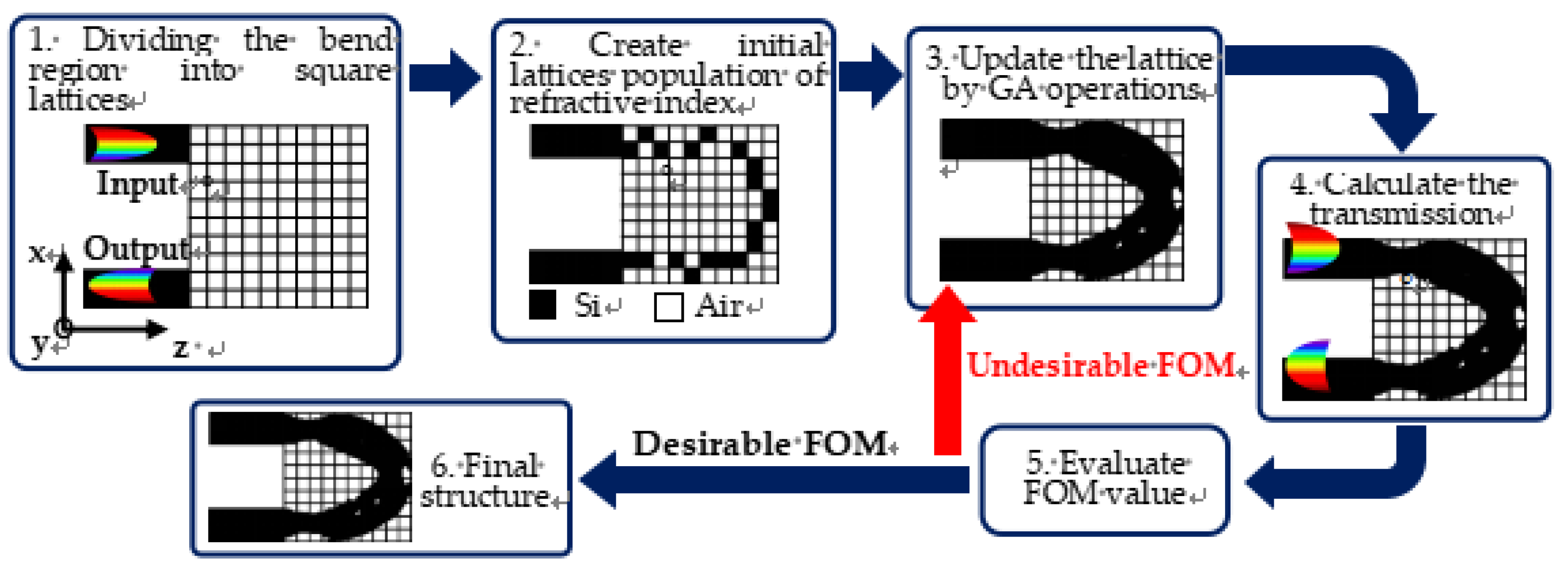
Figure 2.
3D-Schematic of silicon-based 180-degree waveguide bend using digital metamaterials. (a) The all-view schematic diagram of the 180-degree waveguide bend. (b) The Epsilon distribution using digital metamaterials in pattern region.
Figure 2.
3D-Schematic of silicon-based 180-degree waveguide bend using digital metamaterials. (a) The all-view schematic diagram of the 180-degree waveguide bend. (b) The Epsilon distribution using digital metamaterials in pattern region.
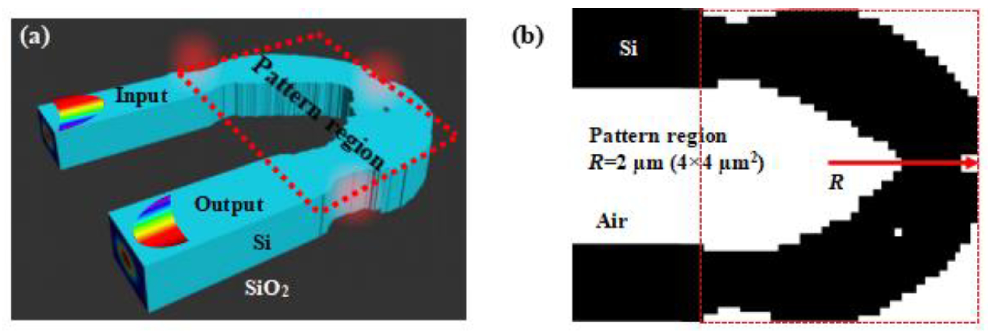
Figure 3.
Simulated light propagation in the designed 180-degree waveguide bend when launching the TE0 (a), TE1 (b), TM0 (c), and TM1 (d) modes, respectively.
Figure 3.
Simulated light propagation in the designed 180-degree waveguide bend when launching the TE0 (a), TE1 (b), TM0 (c), and TM1 (d) modes, respectively.
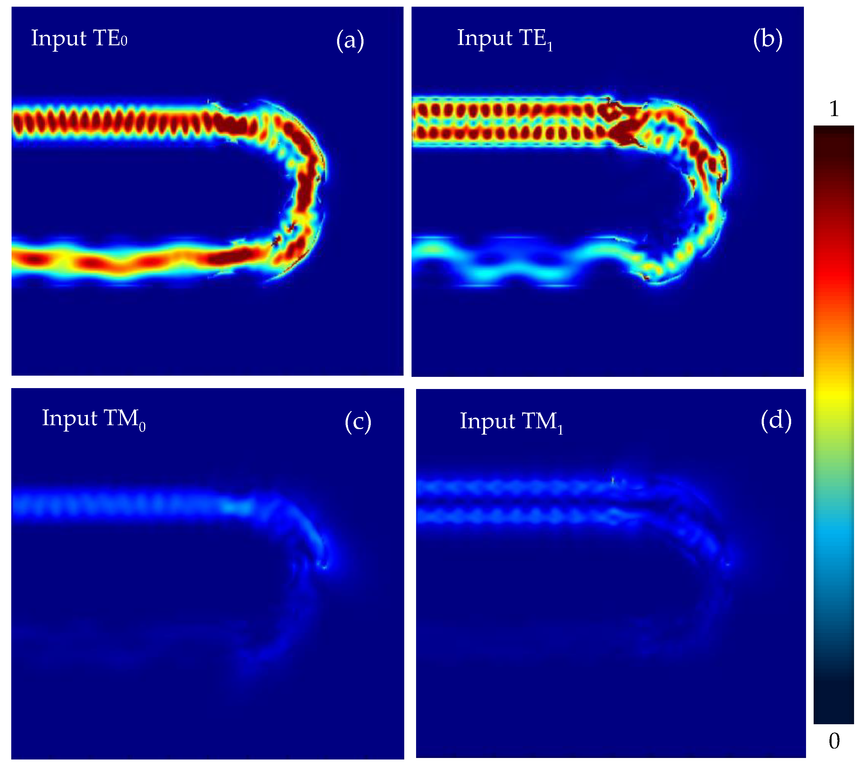
Figure 4.
The transmittance spectra when the TE0 (a), TE1 (b), TM0 (c), TM1 (d) modes are launched from the input end.
Figure 4.
The transmittance spectra when the TE0 (a), TE1 (b), TM0 (c), TM1 (d) modes are launched from the input end.
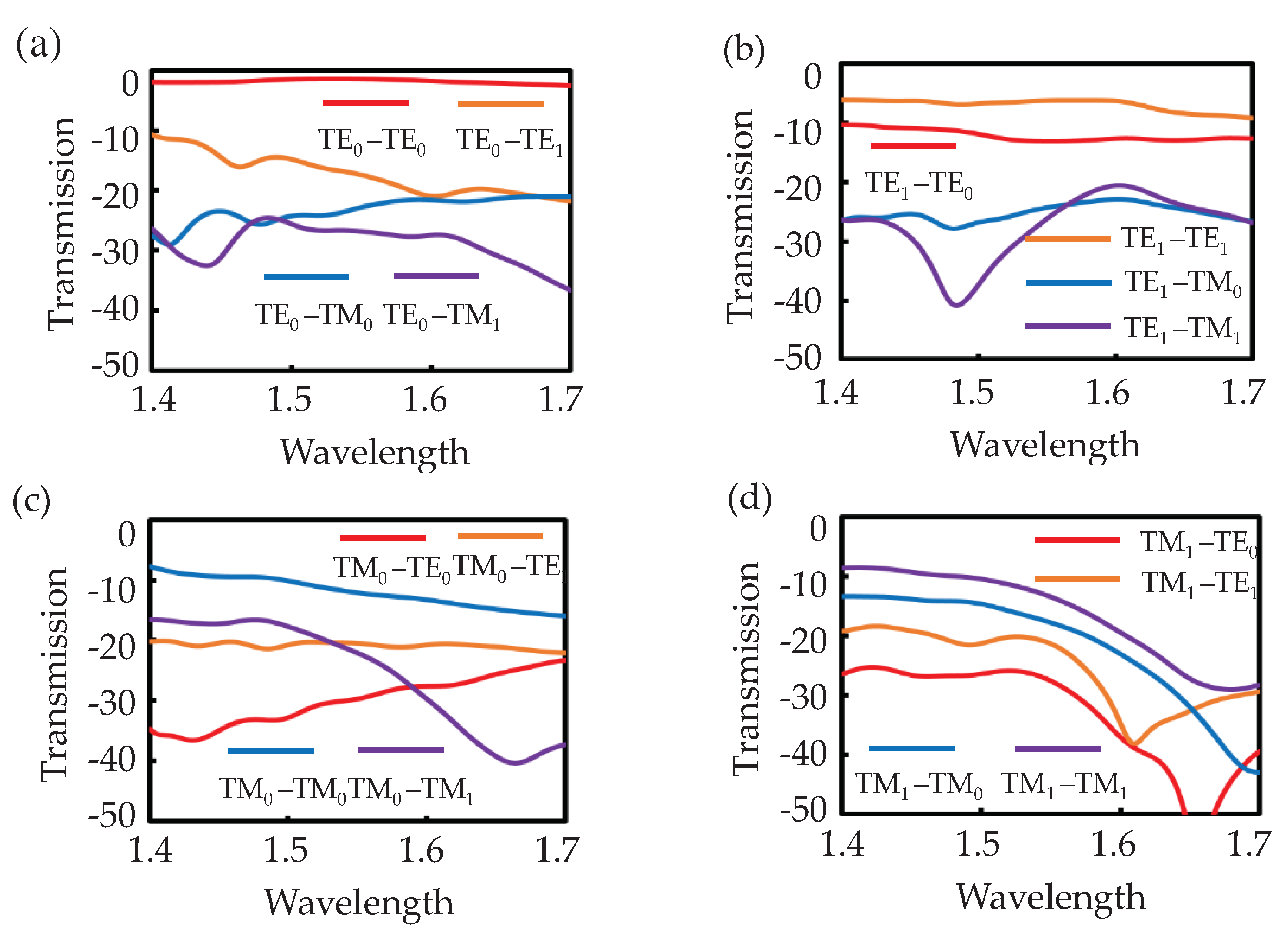

Table 1.
Performance comparison of the presented 180-degree waveguide bends to the state-of-the-art bend waveguides.
Table 1.
Performance comparison of the presented 180-degree waveguide bends to the state-of-the-art bend waveguides.
| References | Transmission (dB/180°) |
Radius (μm) |
1 dB-Bandwidth (μm) |
Footprint (μm2) |
|---|---|---|---|---|
| Xu et al [29] | <-1 | 30 | 0.08 | 60 × 100 |
| Vogelbacher [25] | -0.047 | 40 | λ0= 0.85 | 40 × 80 |
| AI-Tarawni [24] | -0.018 | 5 | λ0= 1.55 | 5 × 10 |
| Bahadori [11] | -0.004 | 5 | λ0= 1.55 | 5 × 10 |
| Our design | -1.36 | 2 | 0.1 | 4 × 4 |
Disclaimer/Publisher’s Note: The statements, opinions and data contained in all publications are solely those of the individual author(s) and contributor(s) and not of MDPI and/or the editor(s). MDPI and/or the editor(s) disclaim responsibility for any injury to people or property resulting from any ideas, methods, instructions or products referred to in the content. |
© 2023 by the authors. Licensee MDPI, Basel, Switzerland. This article is an open access article distributed under the terms and conditions of the Creative Commons Attribution (CC BY) license (http://creativecommons.org/licenses/by/4.0/).
Copyright: This open access article is published under a Creative Commons CC BY 4.0 license, which permit the free download, distribution, and reuse, provided that the author and preprint are cited in any reuse.