
Submitted:
07 October 2023
Posted:
07 October 2023
You are already at the latest version
Abstract
The paper investigates into the intricacies of semiconductor manufacturing, a highly complex process entailing a wide array of subprocesses and diverse equipment. Semiconductors are miniaturized integrated circuits comprising numerous components. The semiconductor manufacturing process begins with the thin disc-shaped silicon wafers. On each wafer, up to thousands of identical chips can be prepared depending upon the diameter of the wafer to build up the circuits layer by layer in a wafer fab. The size of the semiconductors requires a high number of units to be produced, thus necessitating a large amount of data to control for improving the semiconductor manufacturing process. Therefore, the collection and analysis of the equipment data, process data, and machine history data throughout the manufacturing process are required to diagnose faults, monitor the process, and manage the manufacturing process effectively. This research is focused on improving the semiconductor manufacturing process through a rigorous analysis of collected manufacturing process data, employing statistical process control (SPC), data mining techniques, and data-driven decision models. The project's primary objective is to increase the manufacturing process stability and productivity by utilizing the latest data-driven technologies in the scientific community. A structured review was undertaken, exploring contemporary data-driven methodologies in semiconductor manufacturing process improvement, specifically pertaining to process capability, product yield rate, and process stability. This review accentuates a comprehensive evaluation of data-driven methodologies applicable to conventional semiconductor manufacturing facilities, aiming to drive substantial process improvements. It features a detailed demonstration facilitating the selection of optimal semiconductor manufacturing processes to enhance overall operational performance. This study of process improvement in the semiconductor manufacturing steps through the application of data-driven methodologies will be effective in delivering advanced, real-time, and proactive control decisions throughout the manufacturing facilities. This endeavor is expected to promptly provide critical insights for enterprise manufacturing decision-makers to reduce manufacturing cycle time, improve the product yield rate, and increase the overall efficiency of the manufacturing process.
Keywords:
semiconductor manufacturing
; statistical process control (SPC)
; data mining techniques
; data-driven decision models
; process improvement
; product yield rate
; process stability
1. Introduction
Semiconductor manufacturing is a very complicated process that involves a large number of subprocesses and a wide range of equipment. Thin disc-shaped silicon wafers are used to start the semiconductor manufacturing process. The scale of semiconductors necessitates the production of a huge number of units, necessitating a big quantity of data to regulate in order to improve the semiconductor manufacturing process. Since semiconductor manufacturing methods have shrunk in size over the last few years, the transistors produced on single wafer has increased towards billions [1]. The previous several decades have seen the emergence of a wide range of electrical and electronic equipment-related products and services, as well as the incorporation of these equipment into a wide range of products and services that are constantly changing [2]. So the companies of this industry must be flexible and able to react swiftly to a continuously changing environment [3].
Semiconductor manufacturing is the process of creating integrated circuits in electrical devices and consumer electronics, such as transistors, LEDs, and diodes. The crystalline silicon ingot and wafers are formed during the front-end process, and the electrical circuits are built using photolithography and other chemical procedures before being electrically tested. The chunks are sliced off the wafer, connected (glued), encased, and tested in the back-end process [4].
The term "semiconductor" refers to an important component present in electrical devices and widely used in industries. Smartphones, wearable gadgets, and mobile devices all rely on semiconductors for basic and enhanced functionality, resulting in increased global semiconductor demand. The line width of semiconductors has shrunk dramatically, moving from the microscale to the nanoscale, while process power and memory have grown at the same time. Integrated circuits, which are comprised of semiconductor material, are a crucial component of modern electronic gadgets in both the commercial and consumer markets. To conduct fundamental arithmetic operations in a computer, these circuits must be able to operate as transistor.
Several phases in the semiconductor device manufacturing process are conducted in the sophisticated manufacturing units. The time it takes to create a semiconductor varies depending on its complexity, but it typically takes 3 to 5 years from initial research to final product.
The most significant resource for the creation of microelectronic components is very pure silicon. The manufacturing process is depicted in a simplified form in Figure 1 [5]. The initial stage in making a semiconductor device is to get semiconductor materials with the required degree of impurities, such as germanium, gallium arsenide, and silicon [6, 7]. Because semiconductors are so small, even the tiniest amount of contamination can degrade their performance. The somewhat harsh solutions used in the semiconductor manufacturing process should be conveyed, distributed, and handled safely [8].
The development of monocrystalline silicon crystals and multicrystalline ingots is the second major phase. Wafers are then cut from these ingots, then shaped, polished, and cleaned before being ready for further processing or device fabrication [9]. A preceding design procedure for each of the phases, as well as a mask design, is required to generate a working device with set parameters as a final output [10].
Extreme ultraviolet (EUV) lithography, as shown in Figure 1, is one of the most significant phases in semiconductor production because it enables the carving of more electrical circuits in semiconductor silicon wafers. Images are transferred to silicon using light in a lithographic technique [11, 12]. EUV lithography is considered critical in semiconductor manufacturing because it can generate a shorter wavelength, allowing more electrical circuits to fit into a chip [13]. Then there's an etching process, which is a microfabrication technique that involves chemically removing layers of material from a wafer's surface.
The next step is wafer probing, which involves electrically checking each die on a wafer. This is done through the use of an automated wafer probing system that actively searches for functional flaws using particular test patterns [14-16]. The semiconductor packaging and assembly process encloses ICs and includes, among other things. The encapsulation method protects the delicate layers from extraneous influences and ensures that they remain effective [17, 18]. Finally, the completed component is thoroughly examined to ensure that it complies with standard criteria. In the context of design verification, specialized manufacturing, and quality control, the testing procedure is used to test semiconductors [19].
2. Motivation
Industry 4.0 is a concept that entails using data mining techniques, big data, deep learning, and artificial intelligence technology to the present industrial structure in order to produce disruptive breakthroughs [20]. As predicted by the industry 4.0 idea, the purpose of this strategy is to enable flexible decision-making and smart manufacturing processes. As a result, along with Internet of Things (IoT), other emerging technologies will play key part in making Industry 4.0 a reality [21]. In semiconductor manufacturing systems, like in other production technologies, the trend toward unmanned operations, increased automation and substitution of traditional materials has been steadily expanding [22, 23].
Traditionally, semiconductor manufacturing systems have been associated with convoluted and time-consuming process. Wafers often entail a large number of steps, which can frequently exceed a thousand [24, 25]. Every phase is usually equated to a medium-sized industrial unit in terms of complexity. As a result, increased demands and pressure to operate at high plant productivity provide a significant task for semiconductor manufacturing businesses [2].
Semiconductor businesses are fully aware of the ever-increasing need for integrated circuits that can give more performance at lower costs. As a result, wafer metrology tools are used in the design and manufacture of semiconductors for enhancing manufacturing process. Additionally, data-driven methods ensure that the electrical and physical characteristics of generated semiconductors are as near to the desired outcome as possible. Wafer metrology combined with data-driven techniques can reliably and rapidly identify surface pattern errors, particulates, and other situations that might degrade semiconductor performance [26].
Data-driven technologies in semiconductor manufacturing can discover and deliver systematic enterprise knowledge by investigating manufacturing and production system application databases and connecting several databases inside the organization to expose information. The methods can increase product yield rate by predicting parameter settings for future production cycle and computing the best process parameters, boosting manufacturing stability and improving product quality. By calculating process parameters in real-time and delivering automatic feedback to save personnel and increase manufacturing efficiency, the approaches can cut production cycle time and improve efficiency. Data-driven techniques can examine the links between obtained parameters and identify specific patterns or parameter qualities to utilize as production references, decreasing the number of product testing necessary. These strategies create a data model based on the decision-makers' needs and make historical data available through an integrated storage environment with query and analytical capabilities to offer information for corporate manufacturing decision-making as rapidly as feasible [27].
Semiconductor manufacturing has traditionally been regarded to be a fiercely competitive business with expensive equipment and complicated operating and production circumstances [28]. Because the demand for electronic products is continually expanding, manufacturers' capabilities are restricted, and the market is extremely competitive, maintaining a high level of productivity is critical to maintaining a competitive edge. Semiconductor manufacturing has long been noted for its equipment-intensive manufacturing procedures. Consequently, manufacturing organizations have a technological and organizational difficulty in meeting rising demands for high plant productivity.
With the consideration of the complexity of the semiconductor manufacturing, the objective of this project is to utilize newest data-driven technologies in the scientific community to improve manufacturing process stability and productivity. The project's focus has been on a thorough examination of data-driven approaches that may be used to improve traditional semiconductor production facilities. This analysis includes an in-depth explanation of how to choose an efficient semiconductor manufacturing method that will increase the process' overall performance. This detailed project includes identifying improvement scopes and assisting in the selection of required improvement actions. The use of data-driven approaches to process optimization in semiconductor manufacturing processes will be beneficial in offering enhanced, real-time, and proactive control choices throughout production facilities. The initiative will instantly give data to corporate production decision-makers to help them shorten manufacturing cycle times, enhance product yield rates, and improve overall manufacturing process efficiency.
3. Principles
3.1. Data Mining
Data mining is the process of extracting substantial and implicit previously unknown and possibly useful information from data. It can identify patterns in massive amounts of data. The process can sort and categorize data, also search big data sets for anomalies, trends, and correlations in order to predict outcomes. Companies may utilize this data for a number of purposes, including problem identification, quality control, increasing revenue, cutting expenses, improving customer relationships, and reducing risk [29]. Because contemporary semiconductor production processes are so complicated, and the data size is so large, it's hard for achieving rapid yield increase by physically finding relevant patterns in raw data [26]. Nonetheless, in modern manufacturing units like semiconductor fabrication, many elements and features are interrelated and affect the yield of the generated wafers [30]. As a result, the data mining methods can help with the varied issues in semiconductor manufacturing, including the yield development [4, 26], quality checking [31], fault recognition [32], predictive maintenance [33], metrology [34], scheduling [35], business enhancement [36], and market prediction [37], among others.
Despite the fact that there are numerous studies on data mining approaches in the manufacturing process of semiconductor, a gap in the literature was identified after compiling all published studies into a single paper without regard to location or characteristics. The goal of Espadinha-Cruz et al. was to assemble all existing articles on this issue on Scopus and WoS, classify them, and compare them in order to fill the identified research gap. As a result, one of the objectives of this research was to learn about the current status of data mining solutions for semiconductor manufacturing difficulties. In semiconductor manufacturing, data mining has a wide range of uses. The research is divided into categories based on the areas of following applications.
3.1.1. Data Mining Applications for Quality Control
The fundamental goal of quality prediction tools is to foresee product behavior and to predict trends of the crucial parameters. This is often performed by using learning functions that can derive knowledge from previous data. Forecasting quality using data mining techniques often begins with the creation of a model based on past data [38].
3.1.2. Data Mining Applications for Maintenance
A multiple classifier method is presented for predictive maintenance [39] and a similar study is proposed in [33]. Predictive maintenance based on hidden Markov model is presented in another study over a one-year timeframe [40]. A data mining strategy for improved yield management is proposed and proved its efficacy [41]. The final research emphasizes on increased resolution and detection of faulty and malfunctioning equipment, and it is applied by Advanced Micro Devices, Inc. (AMD).
3.1.3. Data Mining Applications for Metrology, Measurement, and Instrumentation
Virtual metrology is an important issue, and it is described as a set of methodologies for estimating the qualities of a wafer using machine data rather than costly physical measurements [42-44]. Because of the fact that machine data is sampled much more frequently than metrology data, and also machine data is immediately available, unlike metrology data. A few feature extraction approaches for virtual metrology using sensor data have been presented in [34, 45, 46].
Different types of measurement and instrumentation are also presented and categorized. For example, a real-time data mining solution is presented for extracting defects from the production data of raw wafer probe test automatically and correctly [47]. A data mining strategy is also described, which employs machine learning algorithms to model unknown functional interrelations and predict the thickness of dielectric layers of manufactured wafers [48]. Finally, IBM created a data mining technique for detecting and exploring correlations between inline measurements and test results in analog and/or radio frequency (RF) devices [49]. This approach is put to use and validated in the real world.
3.1.4. Data Mining Applications for Decision Support Systems
The usage of decision support systems (DSS) is another development in semiconductor production. A DSS is a system that aids in the resolution of unstructured and semi structured managerial challenges at all phases of the decision-making process. This isn't the first time the DSS has been used in this situation. The first articles in this field were published in the 1990s. DSSs may have a knowledge base, which necessitates the use of artificial intelligence to give information to aid the decision-making process. Nevertheless, the first applications of DSS necessitated knowledge modeling from documented and expert information by knowledge engineers. It was possible to find hidden information in enormous volumes of data by extracting knowledge from unprocessed data. Researchers use data mining tools to look for trends and hidden relationships that might help them make better semiconductor decisions. The purpose is usually to establish relationships between control parameters and product quality, mostly through decision rules [5].
3.1.5. Data Mining Applications for Production and Production Scheduling
The purpose of much production planning research is to reduce cycle time. To avoid work in progress (WIP) bubbles and improve cycle time, a unique approach capable of using data mining has been presented [50]. A novel technique capable of incorporating data mining was proposed a with the goal of eliminating work in progress (WIP) bubbles and shorten process times [51]. In semiconductor production system, a data-mining technique is provided for calculating the interval cycle time of each task [52]. Furthermore, a data mining approach for identifying essential components of the cycle time in a semiconductor manufacturing plant with the purpose of estimating its value has been addressed [53].
Semiconductor wafers are manufactured in a series of sequential processes. The process stages having a significant association with wafer yield are known as critical process steps. Because wafer yield is such an important metric in wafer production, it's important to pick and control the critical process steps properly. Lee et al. provided a method for identifying critical process steps that were methodical and data driven.
The method of Lee et al. is in line with the current semiconductor industry trend. The anticipated technique assesses 3 aspects of data from wafer production process utilizing data mining tools. They used the SECOM dataset as a case study for assessing the effect of their recommended method at various missing value rates. The suggested method's technique is depicted in Figure 2.
They used a hypothetical operational data set as a case study and found that the proposed strategy performed effectively [24].
3.2. Artificial Intelligence
A data-driven decision method was presented by Senoner et al. to improve the process quality. Handling high-dimensional and nonlinear production data is a problem for standard quality management approaches. This obstacle was overcome by using explainable artificial intelligence (AI) to quality management. They proposed using nonlinear modeling using Shapley additive explanations (SHAP) values to infer how a collection of production parameters and a manufacturing system’s process quality are linked. As a result, they offered a metric for determining the importance of processes, which manufacturers may use to prioritize processes for quality improvement. Their decision methodology, which was based on quality management theory, chose improvement activities that targeted the sources of quality variance. The decision model has been proven in a real-world application at a prominent high-power semiconductor factory. They used their decision model to choose improvement activities for a transistor chip product in order to enhance production yield. They next conducted a field experiment to ensure that the improvement efforts were effective. The investigation showed a 21.7% reduction in yield loss when compared to the average yield in our sample. They also shared findings from a post-experimental roll-out of the decision model, which resulted in considerable yield increases. They illustrated the practical usefulness of explainable artificial intelligence by demonstrating that traditional methodologies might miss crucial drivers of process quality [54].
3.3. Computer-integrated manufacturing (CIM)
The semiconductor production process has advanced extensively to allow the Internet of Things. One of the major issues in wafer manufacturing is quality improvement. CIM emerged as a way to decrease the rework and enhance manufacturing process over time. To evaluate the acquired semiconductor process data, Li et al. used data mining approaches and statistical process control (SPC). The research extends manufacturing capabilities, increases the yielding rate, and lowers overall cost. The focus of this research is on wafer manufacturing facilities. Between CIM and the manufacturing execution system, a data mining architecture is developed. The system can forecast the best process parameters for the next batch using a mix of real-time feedback and SPC utilizing past process data. The system adapts dynamically for variances between different machines and goods, allowing each machine a degree of flexibility in product manufacture. The suggested semiconductor system may be used to analyze processes in the traditional manufacturing business. Their findings demonstrate how their technology may enhance semiconductor production process, giving the wafer fab a competitive edge [27].
3.4. Machine Learning Algorithms
The intricacy of semiconductor manufacturing creates difficulty on plant availability requirements in this competitive sector. Biebl et al. addressed these issues in their paper by developing a conceptual model for prescriptive maintenance in semiconductor production. To estimate unexpected downtimes, several Machine Learning Algorithms were applied. Furthermore, Bayesian Networks were utilized to forecast the underlying cause of a failure [2].
3.5. Big-Data-Based Monitoring System
Nakata et al. focused their study on yield exploration task to determine the failure reason using failure patterns and production history.
3.5.1. Failure Map Pattern Monitoring by Clustering
At first, they implemented a clustering algorithm to track failure map patterns. Clustering is an unsupervised learning technique that divides things into clusters. K-Means clustering is one of the most basic and often used clustering algorithms. Wafers with analogous failure patterns were grouped using a clustering technique that included K-Means. Engineers may comprehend failure incidence without verifying every wafer by sight since each cluster size immediately shows wafer amount along with the failure pattern.
3.5.2. Failure Cause Identification
Second, the research team used a pattern mining approach to identify the causative devices of failure patterns. Typically, engineers look at a large quantity of production history data, such as which devices wafers have passed through throughout each step.
3.5.3. Failure Recurrence Monitoring
Finally, Finally, they presented a Deep Learning technique for monitoring failure recurrences. In recent studies, machine learning approaches have been used to classify failure map patterns. With the supervised learning strategy, the models automatically categorize fresh wafers and reveal a long-term trend of failure incidence.
Big data analysis provides inclusive monitoring automation, which is the most crucial aspect to remember. They implemented daily thorough monitoring with enormous production data using quick and scalable clustering and pattern mining technologies. They also investigated the performance of deep learning, which has been a popular machine learning core technique in recent years, in the categorization of wafer failure map patterns [26].
3.6. Internet of Things (IOT) and Big Data Analytics
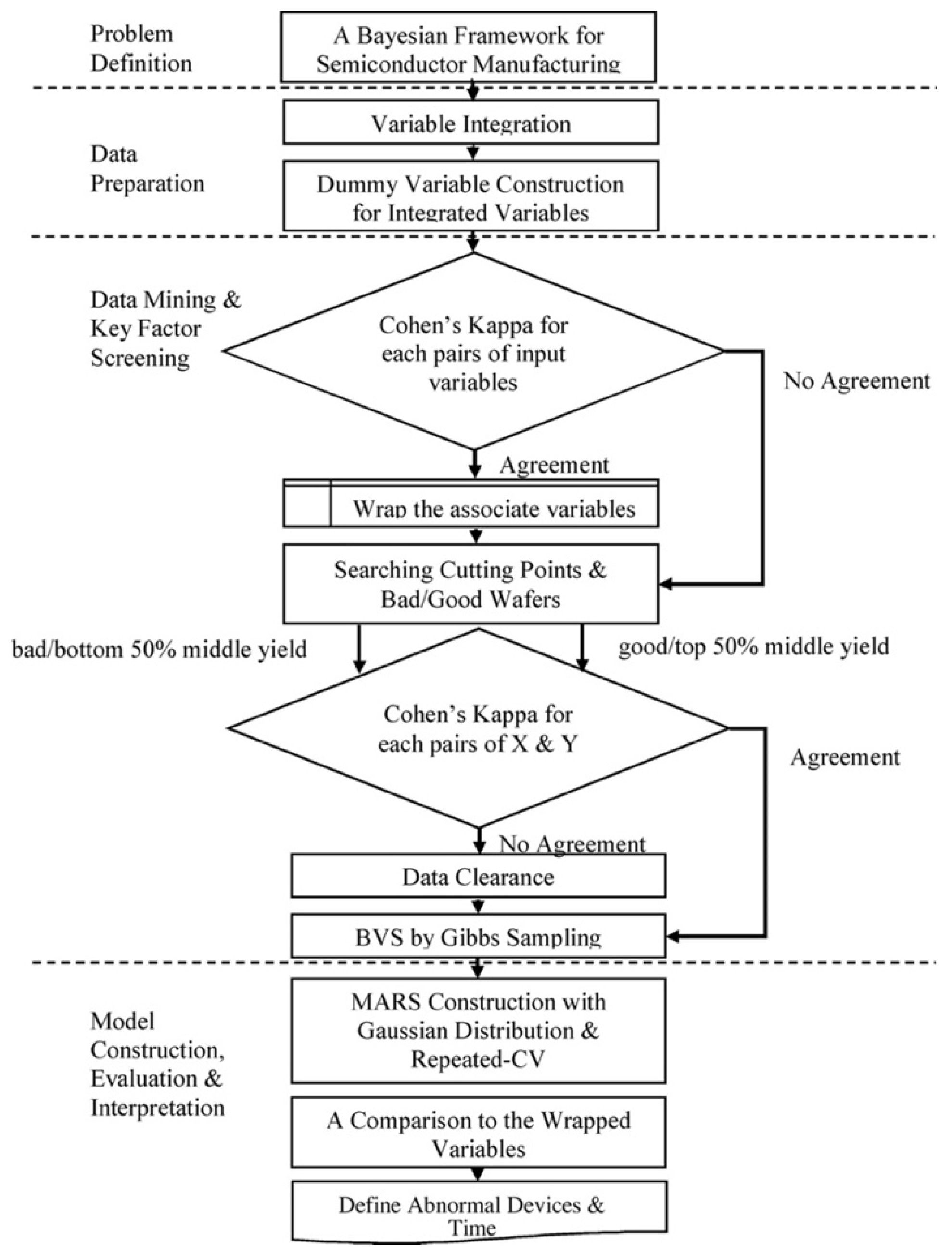
The IoT and big data analytics for semiconductor production have been facilitated by the increased usage of multi featured sensors, complex equipment, and robots. Khakifirooz et al. developed a methodology to explore the complex semiconductor production data for defect identification and intelligent manufacturing. A data-mining framework was developed in the study to analyze vast amounts of semiconductor manufacturing data in order to discover insufficient tool-chamber at a given production period. The four main processes are provided in Figure 3.
An empirical investigation and simulation were used to validate the suggested method. The outcomes demonstrated that the recommended strategy is feasible in practice [4].
The process of optimizing manufacturing processes through the integration of cyber-physical systems and the utilization of data, particularly big data, is referred to as smart manufacturing (SM). Because SM adoption has been unequal among sectors, there is a chance to turn to other industries for solutions and roadmaps for industries like biochemistry and biology. The growth of big data allows for the management of considerably bigger volumes of data and the use of analytics to enhance diagnoses and prognostics. Analytical capabilities will be enhanced in the future by a better big data environment that incorporates smart manufacturing ideas like the digital twin [55].
4. Reviews
The study of Espadinha-Cruz et al. has following points on data mining applications in semiconductor production.
- First, few studies exist for research on wafer cutting, cleaning, drying, and polishing, although there is no specialized study on edge rounding and lapping. Only a few research identify in which subprocesses, data mining methods are used.
- The varied application of data mining techniques is another trend seen in the reviewed literature. However, most articles focus on quality control, maintenance, and manufacturing. In the semiconductor literature, predictive approaches for estimating wafer standard [56], defect identification [57, 58], or process time [59]. In quality control, classification algorithms are used to categorize defects [60], failures of bin maps [61], or lots. Techniques are used to investigate the causes of yield loss or failure diagnostics [5].
Data is collected from different sources in a real-world semiconductor production line. Sensor information is frequently noisy owing to unreliable functioning or data transfer. Considering the data source, there are multiple data types. The study of Lee et al. considered that only quantitative data exists in the proposed problem, with no noisy data. So various data formats should be explored. Human inspection information, for example, is frequently text data in the form of words [62]. Word2vec, an open-source program may be used in this context. This suggested method's distance measure may be substituted by the similarity index. Then, depending on the estimated similarity index, the key traits may be chosen.
Qualitative data is another sort of data that is frequently seen in real-world circumstances. The data collected by the inspection machines are qualitative in nature. The percentage of damaged chips must have been computed when using this qualitative data to the suggested approach. The suggested method's distance measure may then be adjusted by novel method, similar to text data example [24].
Senoner et al. suggested a data-driven decision approach for enhancing semiconductor manufacturing process quality. The decision model has three qualities that overcome the shortcomings of conventional quality modeling methodologies. First, it is strongly associated with quality management theory to focus on the sources of variance before deciding on quality improvement initiatives. Second, it's built to deal with both high-dimensional and nonlinear production data. Third, it provides a metric for process significance, allowing manufacturers to prioritize processes for quality improvement without having access to quality variables gathered during intermediate inspections. Even when manufacturing data is prone to nonlinearities, their estimate of process relevance aids in the appropriate allocation of improvement efforts. They gave evidence from two distinct interventions where typical quality management methodologies failed to give adequate insights into the real-world application at Hitachi ABB. The suggested decision model, on the other hand, highlighted crucial linkages that led to considerable quality increases. They also offered a simulation to show that their process significance metric is useful in detecting quality drivers in nonlinearities. Overall, the practical utility of explainable AI is demonstrated by the field study [54].
The system architecture suggested by Li et al. can be used to analyze traditional semiconductor production processes. Their research contributes to a number of ways. Their technique enables the automation of the semiconductor production process, which can improve a product's yield rate. Parameter optimization can be used to improve a manufacturing process' overall capabilities. This technology provides increased stability and flexibility for semiconductor foundry, giving the firm a competitive advantage. Manufacturing costs can be decreased even while yield rates rise [27].
Nakata et al. concentrated on the yield analysis job in their research. To assist engineers, they used data-driven tools to analyze failure patterns, identify causes, and track failure recurrences. In addition, they used Deep Learning to classify wafer failure map patterns. They evaluated operational variables for assisting engineers' work. Their approach is predicted towards significant labor savings for engineers and a significant increase in output [26]. Data clearing and variable selection, in addition to data preparation, are important processes, however, the techniques take a long time. The structure of Khakifirooz et al. coupled a Bayesian technique with statistical conclusions and a data-mining viewpoint for investigating complicated production data [4]. A new Gibbs sampler method has been developed for speedier interactions within the production system, according to recent research [63]. The analytics environment in semiconductor manufacture is evolving, partly because of SM mandates and innovation, but also as a result of the growth of big data within manufacturing.
The form of analysis, known as artificial neural networks (ANN), has been around for decades. As part of the big data movement, certain forms of AI analytics have experienced a return. Deep Learning, for example, is a technique that uses hierarchical abstraction to improve the process. It is quite similar to structured ANN [64]. In big data contexts, deep learning algorithms profit from larger data quantities and employ approaches to uncover links. Furthermore, because established models are rarely made publicly available, assessing their future resilience might be challenging. Recently, research has been concentrated on merging SME with AI approaches; these techniques have the potential to be applied on the production floor in the future.
5. Applications
To deal with the semiconductor industry's data restrictions and problems, the semiconductor industry's growth is heavily reliant on big data. By allowing bigger volumes and longer archives of data, many systems have been able to accurately cover the system dynamics for decreasing interruptions and solving quality problems. Data mining techniques must be adjusted in these systems to take use of the parallel computation [55]. Researchers and practitioners must adjust data mining techniques so that they may be tailored to individual applications in terms of data integrity.
Hundreds of sophisticated procedures entail towards making semiconductor wafers. Critical process steps have a significant association with wafer yield. Because they have such a big impact on wafer yield, the essential stages should be carefully chosen and handled. The selection criteria, on the other hand, are frequently unclear and rely on the process engineers' expertise and intuition. In practice, critical characteristics (i.e., important process stages) are frequently chosen based on domain experts' understanding. Domain expertise is usually beneficial and helps when selecting essential features. It is, however, sometimes difficult to give quantitative proof of domain expertise. Lee et al. predicted that the suggested technique would choose most of the characteristics chosen by domain experts. The suggested approach can be utilized for providing quantitative data to back up the domain expert's view. Furthermore, when domain experts lack sufficient understanding of the process (as is typically the case when new processes are built), the suggested method's collection of important characteristics may be used like guide for selecting critical features [24].
The study of Espadinha-Cruz et al. offered some insight on the potential uses of data mining techniques in semiconductor production by analyzing enormous volumes of data and exposing previously unseen connections and opportunities. Decision-makers, on the other hand, must select which data should be collected and used [66]. Because these approaches are always evolving, the necessity to adapt them to newer semiconductor production processes is another opportunity to investigate [5].
The decision model of Senoner et al. can be effectively implemented into quality management practice. As a result, manufacturers may get fresh insights from data that is frequently underutilized. [67, 68]. They don't make any assumptions about which meta-model is being utilized. This allows for the simple application of well-known models from the operations management literature [69-71]. They demonstrated that employing a different meta-model (considering equivalent modeling) resulted in identical improvement actions as part of the robustness tests. Furthermore, the decision model is defined in a general way, requiring just minimal input in the form of production data, a measurable process quality variable, and process requirements. Their field study took place in the semiconductor sector, which offers a number of advantages for deploying explainable AI. To begin with, semiconductor production is highly automated, making data collection and system coverage easier. Then, fabrication procedures are well specified, allowing each product to be traced back to a specific technique. Finally, semiconductor producers face significant yield losses, which drives quality improvement efforts [54].
The ultimate goal of prescriptive maintenance model of Biebl et al. is towards the establishment of the optimal point of intervention. Various advantages can be obtained as a result of this. The maintenance time is significantly less than the required time for unexpected maintenance operations since there is no waiting time for replacement parts to be delivered from stock or for a sufficient competent crew to conduct the maintenance activity. Adjusting and prioritizing personnel can considerably minimize this waiting time. Another advantage of verifying spare part availability and spare part orders is that downtime caused by missing spare parts may be prevented [2].
6. Challenges
Data driven technologies have the potential to infringe on people's privacy. It may be extremely harmful to users and lead to misunderstanding among staff, resulting in serious privacy issues [72].
Every data-oriented technology, including semiconductor production, has a significant security component. Malicious attacks may target data that is extremely important [73]. Too much and duplicate data collecting can be detrimental, as identifying unnecessary data can be difficult. Information might be misused as a result of the data-driven process.
Another restriction is the accuracy of data-driven techniques. Accuracy is a measuring method that determines how effectively a data-driven model performs. As a result, enhancing precision becomes critical. In data-driven methodologies, there are a variety of data integration and interoperability difficulties that might arise.
Data interoperability and data integration have an impact on an organization's success. To overcome the issues of interoperability and integration, a complete solution is required.
In this business, missing and skewed data is a problem. As a result of the unbalanced data, the majority of classification algorithms perform poorly. Because wafer yield improvement is such an important metric in semiconductor wafer production, essential process stages must be carefully chosen and regulated.
Data preparation time is another constraint that has a substantial influence on available time, as it accounts for more than half of the time and effort spent on the overall data analysis process [5].
7. Suggestions
Data-driven applications in semiconductor production still have improvement scopes. Semiconductor businesses, for example, might use IoT and machine data for equipping manufacturing units to deliver insights and alarms to those who need them. This will enable the collection of a large amount of information. Moreover, the integration of sustainable practices such as renewable energy adoption and the implementation of circular economy principles within the manufacturing process promises to provide a leading-edge advantage for enhancing the overall process efficiency and sustainability [74-76].
Nonetheless, IoT deployment, and with it, complete use of data mining tools, may be determined by how quickly industry participants solve specific hurdles [5]. Semiconductor firms must adapt quickly to survive and be able to keep up with the rate of change and problems. In light of this dynamic, industrial units should embrace digitization as quickly as possible [77].
However, Lee et al. proposed four potential study paths for determining essential process stages using a systematic and data-driven methodology. Firstly, the suggested method's robustness must be increased. When the missing value rate is large, the suggested technique is susceptible to random deletion trials. In order to improve the robustness of our strategy, it is needed to study other missing data imputation methods. Secondly, evaluation criteria for the important actions that have been chosen must be defined. For instance, indicators for equipment health evaluation might be used [78]. Thirdly, it is required to take continuous values into account while analyzing yield data. In practice, however, the yield has a continuous range of values from 0 to 1. This point can help to perform a more realistic analysis. Finally, the suggested technique may be improved by taking into account the practical industry challenges [24].
Despite the advantages of the research context, the decision model of Senoner et al. generalizes to production settings other than semiconductor manufacture. The most difficult challenge is presenting data that covers all essential operations and manufacturing metrics. There is a danger that quality drivers will go overlooked if essential production metrics are removed. Pharmaceuticals, petrochemicals, and automated manufacturing lines for fast-moving consumer items or printed circuit boards are among the other industries that are expected to benefit. Because manual procedures are typically quality drivers but difficult to capture digitally, the decision model is expected to perform poorly in labor-intensive production. The issues of data representability are projected to be lessened in the future with the ongoing advancement of manufacturing process [54].
Biebl et al. provided a conceptual model that used Machine Learning Algorithms allowed for the prediction of unscheduled downtimes as well as the recommendation of actions on components that may be the root cause. However, a high degree of data and information quality is necessary to properly use the recommended model or alternative techniques in terms of prescriptive maintenance. As a result, maintenance measures must be classified and component-specific documentation of completed orders must be generated [2].
8. Conclusion
The identification and classification of a number of beneficial and successful examples can help future research efforts to apply a wide variety of methodologies in order to increase the data-driven approaches in the industry. Understanding of the data-driven technologies may result in good consequences not only for the development of theory but also for the practical implementation, since most of the methods have been applied and proven on production floor. Nevertheless, numerous applications are still possible because some research focus on a single phase of semiconductor fabrication and real-world application data is lacking. Furthermore, because there are fewer research, contemporary data-driven methodologies and models have a better chance of being adopted. Finally, because the semiconductor manufacturing process is continually changing, adapting these approaches to the current process offers a new problem and opportunity to pursue.
Overall, the implementation of data-driven methodologies should be promoted in order to provide proactive adjustment and advanced control decisions for the whole process and smart facilities in real-time, as evidenced by all of the studies compiled from various stages of semiconductor manufacture. As a result, more research is needed into exploiting and supporting smart manufacturing for fourth industrial revolution across a number of industries to digitally change and update present manufacturing units. This approach will increase choice flexibility while also improving the capacity to optimize related decisions.
References
- Bui, P.-D. and C. Lee, Unified System Network Architecture: Flexible and Area-Efficient NoC Architecture with Multiple Ports and Cores. Electronics, 2020. 9(8): p. 1316. [CrossRef]
- Biebl, F., et al., A conceptual model to enable prescriptive maintenance for etching equipment in semiconductor manufacturing. Procedia CIRP, 2020. 88: p. 64-69. [CrossRef]
- Weber, A., Smart manufacturing in the semiconductor industry: An evolving nexus of business drivers, technologies, and standards, in Smart Manufacturing. 2020, Elsevier. p. 59-105.
- Khakifirooz, M., C.F. Chien, and Y.-J. Chen, Bayesian inference for mining semiconductor manufacturing big data for yield enhancement and smart production to empower industry 4.0. Applied Soft Computing, 2018. 68: p. 990-999.
- Espadinha-Cruz, P., R. Godina, and E.M. Rodrigues, A review of data mining applications in semiconductor manufacturing. Processes, 2021. 9(2): p. 305. [CrossRef]
- Wellmann, P.J., Power electronic semiconductor materials for automotive and energy saving applications–SiC, GaN, Ga2O3, and diamond. Zeitschrift für anorganische und allgemeine Chemie, 2017. 643(21): p. 1312-1322.
- Garlapati, S.K., et al., Printed electronics based on inorganic semiconductors: From processes and materials to devices. Advanced Materials, 2018. 30(40): p. 1707600. [CrossRef]
- Geng, N. and Z. Jiang. Capacity planning for semiconductor wafer fabrication with uncertain demand and capacity. in 2007 IEEE International Conference on Automation Science and Engineering. 2007. IEEE.
- Tilli, M., Silicon wafers preparation and properties, in Handbook of Silicon Based MEMS Materials and Technologies. 2020, Elsevier. p. 93-110.
- Gallagher, E. and M. Hibbs, Masks for micro-and nanolithography, in Nanolithography. 2014, Elsevier. p. 158-178.
- Rice, B., Extreme ultraviolet (EUV) lithography, in Nanolithography. 2014, Elsevier. p. 42-79.
- Marconi, M. and P. Wachulak, Extreme ultraviolet lithography with table top lasers. Progress in Quantum Electronics, 2010. 34(4): p. 173-190. [CrossRef]
- Buitrago, E., et al., EUV lithography process challenges, in Frontiers of Nanoscience. 2016, Elsevier. p. 135-176.
- Chang, H.-Y., et al., Geometric design for ultra-long needle probe card for digital light processing wafer testing. Microelectronics Reliability, 2010. 50(4): p. 556-563. [CrossRef]
- Sakamaki, R. and M. Horibe, Realization of accurate on-wafer measurement using precision probing technique at millimeter-wave frequency. IEEE Transactions on Instrumentation and Measurement, 2018. 67(8): p. 1940-1945. [CrossRef]
- Sakamaki, R. and M. Horibe, Uncertainty analysis method including influence of probe alignment on on-wafer calibration process. IEEE Transactions on Instrumentation and Measurement, 2019. 68(6): p. 1748-1755. [CrossRef]
- Kuo, C.-H., et al., Life cycle impact assessment of semiconductor packaging technologies with emphasis on ball grid array. Journal of Cleaner Production, 2020. 276: p. 124301. [CrossRef]
- Elshabini, A., F. Barlow, and P. Wang, Electronic packaging: semiconductor packages. 2017.
- Sang, H.-Y., P.-Y. Duan, and J.-Q. Li, An effective invasive weed optimization algorithm for scheduling semiconductor final testing problem. Swarm and Evolutionary Computation, 2018. 38: p. 42-53. [CrossRef]
- Reis, M.S. and G. Gins, Industrial process monitoring in the big data/industry 4.0 era: From detection, to diagnosis, to prognosis. Processes, 2017. 5(3): p. 35. [CrossRef]
- Lin, Y.-C., et al., Implementation Criteria for Intelligent Systems in Motor Production Line Process Management. Processes, 2020. 8(5): p. 537. [CrossRef]
- Chen, T., Strengthening the competitiveness and sustainability of a semiconductor manufacturer with cloud manufacturing. Sustainability, 2014. 6(1): p. 251-266. [CrossRef]
- Omer, L., et al. Induction Initiated Curing of Additively Manufactured Thermoset Composites. in Solid Freeform Fabrication 2022: Proceedings of the 33rd Annual International Solid Freeform Fabrication Symposium – An Additive Manufacturing Conference. 2022.
- Lee, D.-H., et al., A data-driven approach to selection of critical process steps in the semiconductor manufacturing process considering missing and imbalanced data. Journal of Manufacturing Systems, 2019. 52: p. 146-156. [CrossRef]
- Hsu, C.-Y., W.-J. Chen, and J.-C. Chien, Similarity matching of wafer bin maps for manufacturing intelligence to empower Industry 3.5 for semiconductor manufacturing. Computers & Industrial Engineering, 2020. 142: p. 106358. [CrossRef]
- Nakata, K., et al., A comprehensive big-data-based monitoring system for yield enhancement in semiconductor manufacturing. IEEE Transactions on Semiconductor Manufacturing, 2017. 30(4): p. 339-344. [CrossRef]
- Li, B., R.-S. Chen, and C.-Y. Liu, Using intelligent technology and real-time feedback algorithm to improve manufacturing process in IoT semiconductor industry. The Journal of Supercomputing, 2021. 77(5): p. 4639-4658. [CrossRef]
- Yang, L. and J. Lee, Bayesian Belief Network-based approach for diagnostics and prognostics of semiconductor manufacturing systems. Robotics and Computer-Integrated Manufacturing, 2012. 28(1): p. 66-74. [CrossRef]
- Yang, X.-S., Introduction to algorithms for data mining and machine learning. 2019: Academic press.
- Chien, C.-F., W.-C. Wang, and J.-C. Cheng, Data mining for yield enhancement in semiconductor manufacturing and an empirical study. Expert Systems with Applications, 2007. 33(1): p. 192-198. [CrossRef]
- He, J. and Y. Zhu. Hierarchical multi-task learning with application to wafer quality prediction. in 2012 IEEE 12th International Conference on Data Mining. 2012. IEEE.
- Jeong, M.K., et al., Wavelet-based data reduction techniques for process fault detection. Technometrics, 2006. 48(1): p. 26-40. [CrossRef]
- Susto, G.A. and A. Beghi. Dealing with time-series data in predictive maintenance problems. in 2016 IEEE 21st International Conference on Emerging Technologies and Factory Automation (ETFA). 2016. IEEE.
- Choi, J. and M.K. Jeong, Deep autoencoder with clipping fusion regularization on multistep process signals for virtual metrology. IEEE sensors letters, 2018. 3(1): p. 1-4. [CrossRef]
- Wenjing, W., et al. Data mining based dynamic scheduling approach for semiconductor manufacturing system. in 2015 34th Chinese Control Conference (CCC). 2015. IEEE.
- Khemiri, A., et al. Improving business process in semiconductor manufacturing by discovering business rules. in 2018 Winter Simulation Conference (WSC). 2018. IEEE.
- Huang, C.-Y. and P.K. Lin, Application of integrated data mining techniques in stock market forecasting. Cogent Economics & Finance, 2014. 2(1): p. 929505. [CrossRef]
- Li, J., et al., A Review of the Applications of Data Mining for Semiconductor Quality Control. Signal and Information Processing, Networking and Computers, 2020: p. 486-492. [CrossRef]
- Susto, G.A., et al., Machine learning for predictive maintenance: A multiple classifier approach. IEEE Transactions on Industrial Informatics, 2014. 11(3): p. 812-820. [CrossRef]
- Kinghorst, J., et al. Hidden Markov model-based predictive maintenance in semiconductor manufacturing: A genetic algorithm approach. in 2017 13th IEEE Conference on Automation Science and Engineering (CASE). 2017. IEEE.
- Hsu, C.-Y., C.-F. Chien, and P.-N. Chen, Manufacturing intelligence for early warning of key equipment excursion for advanced equipment control in semiconductor manufacturing. Journal of the Chinese Institute of Industrial Engineers, 2012. 29(5): p. 303-313. [CrossRef]
- Chen, C.-H., et al., Virtual metrology of semiconductor PVD process based on combination of tree-based ensemble model. ISA transactions, 2020. 103: p. 192-202. [CrossRef]
- Cai, H., et al., Adaptive virtual metrology method based on Just-in-time reference and particle filter for semiconductor manufacturing. Measurement, 2021. 168: p. 108338. [CrossRef]
- Park, C., et al., Multitask learning for virtual metrology in semiconductor manufacturing systems. Computers & Industrial Engineering, 2018. 123: p. 209-219. [CrossRef]
- Maggipinto, M., et al., DeepVM: A Deep Learning-based approach with automatic feature extraction for 2D input data Virtual Metrology. Journal of Process Control, 2019. 84: p. 24-34. [CrossRef]
- Lenz, B., B. Barak, and C. Leicht. Development of smart feature selection for advanced virtual metrology. in 25th Annual SEMI Advanced Semiconductor Manufacturing Conference (ASMC 2014). 2014. IEEE.
- Ooi, M.P.-L., et al., Getting more from the semiconductor test: Data mining with defect-cluster extraction. IEEE Transactions on Instrumentation and Measurement, 2011. 60(10): p. 3300-3317. [CrossRef]
- Lenz, B., et al. Virtual metrology in semiconductor manufacturing by means of predictive machine learning models. in 2013 12th International Conference on Machine Learning and Applications. 2013. IEEE.
- Kupp, N., M. Slamani, and Y. Makris. Correlating inline data with final test outcomes in analog/RF devices. in 2011 Design, Automation & Test in Europe. 2011. IEEE.
- Chien, C.-F., C.-J. Kuo, and C.-M. Yu, Tool allocation to smooth work-in-process for cycle time reduction and an empirical study. Annals of Operations Research, 2020. 290(1): p. 1009-1033. [CrossRef]
- Tirkel, I., Forecasting flow time in semiconductor manufacturing using knowledge discovery in databases. International Journal of Production Research, 2013. 51(18): p. 5536-5548. [CrossRef]
- Lin, Y.C. and T.-C. Chen, Interval cycle time estimation in a semiconductor manufacturing system with a data-mining approach. International Review on Computers and Software, 2009. 4(6): p. 737-742.
- Meidan, Y., et al., Data mining for cycle time key factor identification and prediction in semiconductor manufacturing. IFAC Proceedings Volumes, 2009. 42(4): p. 217-222. [CrossRef]
- Senoner, J., T. Netland, and S. Feuerriegel, Using explainable artificial intelligence to improve process quality: evidence from semiconductor manufacturing. Manag Sci, forthcoming, 2021. [CrossRef]
- Moyne, J. and J. Iskandar, Big data analytics for smart manufacturing: Case studies in semiconductor manufacturing. Processes, 2017. 5(3): p. 39. [CrossRef]
- Zhu, Y., J. He, and R.D. Lawrence, A general framework for predictive tensor modeling with domain knowledge. Data mining and knowledge discovery, 2015. 29(6): p. 1709-1732. [CrossRef]
- Kim, J.K., et al. Feature selection techniques for improving rare class classification in semiconductor manufacturing process. in International Conference on Big Data Technologies and Applications. 2016. Springer.
- Kerdprasop, N. and K. Kerdprasop, Data preparation techniques for improving rare class prediction, in Proceedings of the 13th WSEAS international conference on mathematical methods, computational techniques and intelligent systems, and 10th WSEAS international conference on non-linear analysis, non-linear systems and chaos, and 7th WSEAS international conference on dynamical systems and control, and 11th WSEAS international conference on Wavelet analysis and multirate systems: recent researches in computational techniques, non-linear systems and control. 2011, World Scientific and Engineering Academy and Society (WSEAS): Iasi, Romania. p. 204–209.
- Meidan, Y., et al., Cycle-time key factor identification and prediction in semiconductor manufacturing using machine learning and data mining. IEEE transactions on semiconductor manufacturing, 2011. 24(2): p. 237-248. [CrossRef]
- Haddad, B., et al. Multi-feature sparse-based defect detection and classification in semiconductor units. in 2016 IEEE International Conference on Image Processing (ICIP). 2016. IEEE.
- Chien, C.-F., S.-C. Hsu, and Y.-J. Chen, A system for online detection and classification of wafer bin map defect patterns for manufacturing intelligence. International Journal of Production Research, 2013. 51(8): p. 2324-2338. [CrossRef]
- Zhang, D., et al., Chinese comments sentiment classification based on word2vec and SVMperf. Expert Systems with Applications, 2015. 42(4): p. 1857-1863. [CrossRef]
- Rubinstein, R.Y., A. Ridder, and R. Vaisman, Fast sequential Monte Carlo methods for counting and optimization. 2013: John Wiley & Sons.
- Najafabadi, M.M., et al., Deep learning applications and challenges in big data analytics. Journal of big data, 2015. 2(1): p. 1-21. [CrossRef]
- Moyne, J., J. Samantaray, and M. Armacost, Big data capabilities applied to semiconductor manufacturing advanced process control. IEEE transactions on semiconductor manufacturing, 2016. 29(4): p. 283-291. [CrossRef]
- Anaya, A., et al. Yield Improvement Using Advanced Data Analytics. in 2019 30th Annual SEMI Advanced Semiconductor Manufacturing Conference (ASMC). 2019. IEEE.
- Kusiak, A., Smart manufacturing must embrace big data. Nature, 2017. 544(7648): p. 23-25. [CrossRef]
- Corbett, C.J., How sustainable is big data? Production and Operations Management, 2018. 27(9): p. 1685-1695. [CrossRef]
- Cui, R., et al., The operational value of social media information. Production and Operations Management, 2018. 27(10): p. 1749-1769. [CrossRef]
- Sun, J., et al., Predicting human discretion to adjust algorithmic prescription: A large-scale field experiment in warehouse operations. Management Science, 2021. [CrossRef]
- Bastani, H., D. Zhang, and H. Zhang, Applied machine learning in operations management. Available at SSRN 3736466, 2020.
- Javid, T., M.K. Gupta, and A. Gupta, A hybrid-security model for privacy-enhanced distributed data mining. Journal of King Saud University-Computer and Information Sciences, 2020. [CrossRef]
- Dogan, A. and D. Birant, Machine learning and data mining in manufacturing. Expert Systems with Applications, 2021. 166: p. 114060. [CrossRef]
- Chowdhury, H. and M.T. Islam. Multiple Charger with Adjustable Voltage Using Solar Panel. in International Conference on Mechanical Engineering and Renewable Energy 2015 (ICMERE2015). 2015. Chittagong University of Engineering and Technology.
- Chowdhury, H. and B. Asiabanpour, A Smart Circular Economy for Integrated Organic Hydroponic-Aquaponic Farming. 2023, Texas State University.
- Chowdhury, H., Circular Economy Integration in Additive Manufacturing, in Preprints. 2023, Preprints. [CrossRef]
- Misrudin, F. and L.C. Foong, Digitalization in semiconductor manufacturing-simulation forecaster approach in managing manufacturing line performance. Procedia Manufacturing, 2019. 38: p. 1330-1337. [CrossRef]
- Thieullen, A., M. Ouladsine, and J. Pinaton, A survey of health indicators and data-driven prognosis in semiconductor manufacturing process. IFAC Proceedings Volumes, 2012. 45(20): p. 19-24. [CrossRef]
Figure 1.
The semiconductor manufacturing process is depicted in a simplified form. [5].
Figure 1.
The semiconductor manufacturing process is depicted in a simplified form. [5].
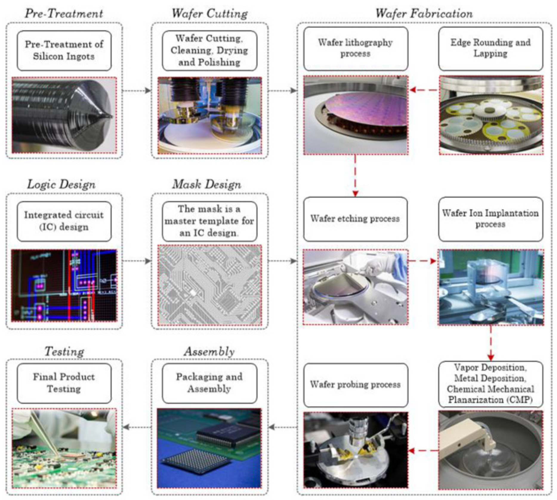
Figure 2.
The proposed methodology of data mining
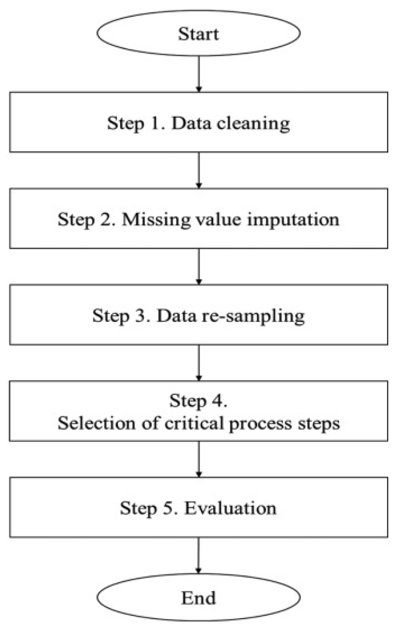
Figure 3.
Research layout of Khakifirooz et al.
Disclaimer/Publisher’s Note: The statements, opinions and data contained in all publications are solely those of the individual author(s) and contributor(s) and not of MDPI and/or the editor(s). MDPI and/or the editor(s) disclaim responsibility for any injury to people or property resulting from any ideas, methods, instructions or products referred to in the content. |
© 2023 by the authors. Licensee MDPI, Basel, Switzerland. This article is an open access article distributed under the terms and conditions of the Creative Commons Attribution (CC BY) license (http://creativecommons.org/licenses/by/4.0/).
Copyright: This open access article is published under a Creative Commons CC BY 4.0 license, which permit the free download, distribution, and reuse, provided that the author and preprint are cited in any reuse.


